

Page 1
查询PT4220供应商
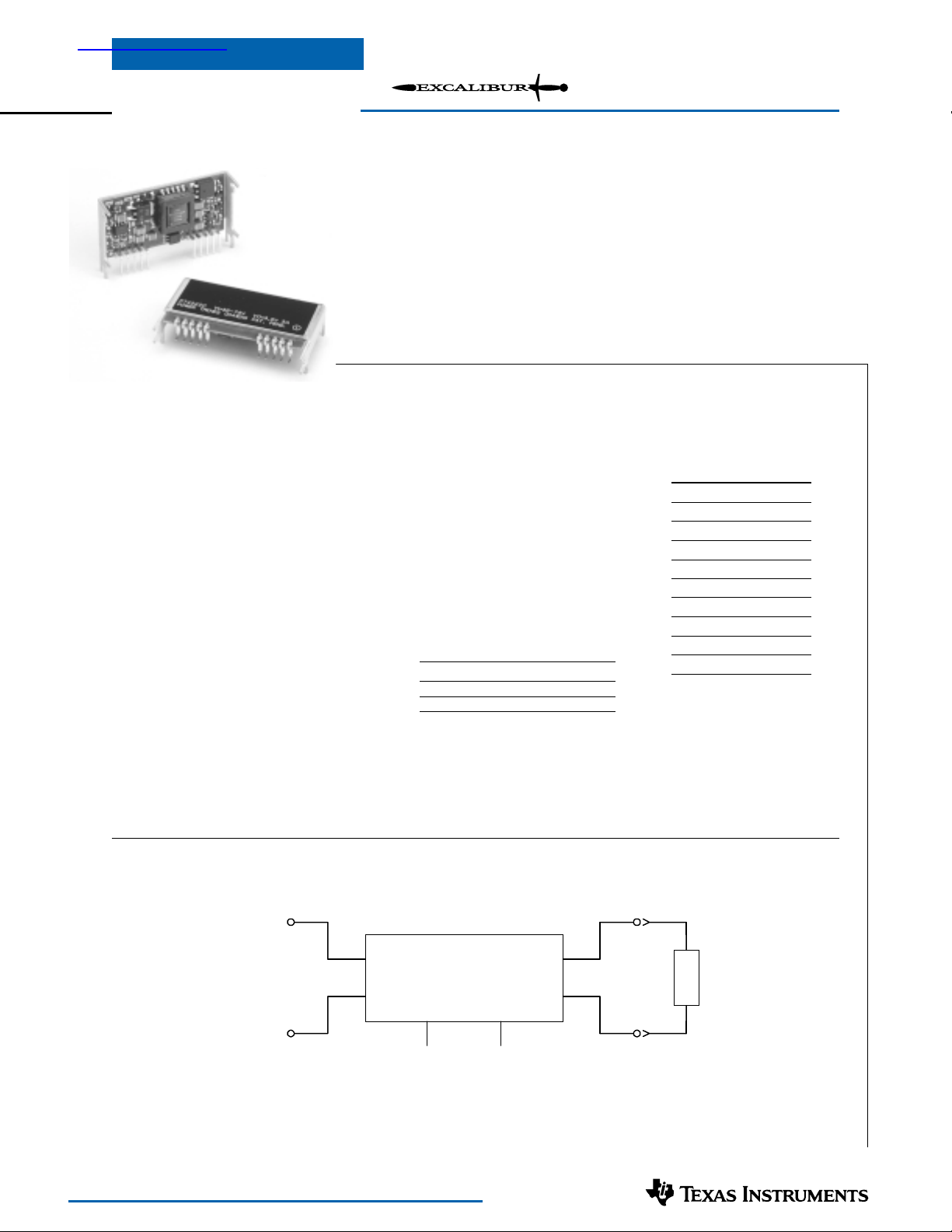
PT4220 Series
10-W Low-Profile 48V-Input
Isolated DC/DC Converter
Description
The PT4220 power modules are a
series of DC/DC converters housed in
an ultra-low profile (8mm) solderable
copper case. The series includes a number of preset output voltages ranging
from 1.3V
for Telecom use. They may also be used
in many other applications that require
input-output isolation over an extended
temperature range. The modules are an
ideal choice for low-power digital and
analog circuits, including DSPs and
microcontrollers. The flexibility of
input-output isolation also allows the
output to be configured for negative
voltage operation.
in both horizontal and vertical pin configurations, including surface mount.
†
up to 12V, all fully approved
The PT4220 series is made available
Features
• 10W Output Power
• Input Voltage: 36V to 75V
• Output Voltages:
1.2V to 13.2V
• 1500 VDC Isolation
• Temp Range: –40°C to +85°C
• Remote On/Off Control
• Undervoltage Lockout
• Output Current Limit
Ordering Information
PT4221¨ =1.8V/3A (5.4W)
PT4222¨ =3.3V/3A
PT4223¨ =5.0V/2A
PT4224¨ =12.0V/0.85A
PT4225¨ =2.5V/3A (7.5W)
PT4226¨ =1.5V/3A (4.5W)
† PT4227¨ =1.3V/3A (3.9W)
† Adjustable to 1.2V
PT Series Suffix
Case/Pin Order Package
Configuration Suffix Code
Vertical N (EPE)
Horizontal A (EPF)
SMD C (EPG)
(Reference the applicable package code drawing for the dimensions and PC board layout)
(PT1234x)
SLTS127A
(Revised 1/14/2002)
• Short-Circuit Protection
• Low-Profile Package (8mm)
• Space Saving Package
• Solderable Copper Case
• Safety Agency Approvals:
UL 60950
CSA 22.2 60950
Pin-Out Information
Pin Function
1 Remote On/Off *
2 Do not connect
3–V
in
4 Do not connect
5+V
in
6-V
out
7-V
out
8+V
out
9+V
out
10 V
Adj *
out
* For further information, see
application notes.
Standard Application
+V
in
58, 9
+Vin
3
-Vin
-V
in
For technical support and more information, see inside back cover or visit www.ti.com
PT4220
Remote
On/Off
1
+V
out
+Vout
6, 7
–Vout
V
(adj)
o
10
-V
L
O
A
D
out
Page 2
PT4220 Series
10-W Low-Profile 48V-Input
Isolated DC/DC Converter
Specifications (Unless otherwise stated, T
=25°C, Vin =48V, Cin =0µF, C
a
=0µF, and Io =Iomax)
out
PT4220 SERIES
Characteristic Symbol Conditions Min Typ Max Units
Output Current I
Input Voltage Range V
o
in
Over Vin range V
Over Io Range 36.0 48.0 75.0 VDC
≤ 3.3V 0.1
o
=5.0V 0.1
V
o
V
= 12V 0.1
o
Set Point Voltage Tolerance Vo tol —±1±2%V
Temperature Variation Reg
Line Regulation Reg
Load Regulation Reg
Total Output Voltage Variation ∆V
temp
line
load
tot Includes set-point, line, load,
o
Efficiency η V
Ripple (pk-pk) V
V
o
Transient Response t
Output Voltage Adjust V
Current Limit Threshold I
Switching Frequency ƒ
∆V
r
tr
tr
adj
lim
s
–40° ≤Ta ≤ +85°C, I
=Iomin — ±0.2 — %V
o
Over Vin range — ±1 — mV
Over Io range — ±5 — mV
–40° ≤Ta ≤ +85°C
= 12 V — 87 —
o
= 5.0V — 85 —
V
o
= 3.3V — 81 —
V
o
= 2.5V — 78 — %
V
o
Vo = 1.8V — 73 —
= 1.5V — 71 —
V
o
Vo = 1.3V — 65 —
20MHz bandwidth V
≤ 5.0V — 50 —
o
V
= 12V — 100 —
o
1A/µs load step, 50% to 100% Iomax — 75 — µs
Vo over/undershoot V
V
=36V, ∆V
in
= –1 % — 150 — %Iomax
o
≤ 5.0V — ±150 —
o
V
= 12V — ±350 —
o
V
≥2.5V ±10 — — %V
o
Over Vin range 250 300 350 kHz
(1)
—3
(1)
—2
(1)
— 0.85
— ±1.5 ±3 %V
mV
mV
o
o
o
pp
o
Under-Voltage Lockout UVLO — 32 — V
Remote On/Off (Pin 1) Referenced to –Vin (pin 3)
Input High Voltage V
Input Low Voltage V
Input Low Current I
IH
IL
IL
4.5 — Open
–0.2 — +0.8
— –0.5 — mA
(3)
V
Standby Input Current Iin standby pins 1 & 3 connected — 1 — mA
Internal Input Capacitance C
External Output Capacitance C
Isolation Voltage Input–output/input–case 1500 — — V
Capacitance Input to output — 1,100 — pF
Resistance Input to output 10 — — MΩ
Operating Temperature Range T
Storage Temperature T
Reliability MTBF Per Bellcore TR-332
Mechanical Shock — Per Mil-Std-883D, method 2002.3, — 500 — G’s
Mechanical Vibration — Mil-Std-883D, Method 2007.2
in
out
a
s
Over Vin range -40 — +85
— -40 — +125 °C
V
≤ 5.0V 0
o
Vo = 12 V 0
50% stress, Ta =40°C, ground benign
1mS, half-sine, mounted to a fixture
20-2000Hz, all case styles soldered to PC
— 0.66 — µF
(5)
— 1000 µF
(5)
— 330
(4)
4.7 — — 10
(6)
— 20
—G’s
°C
6
Hrs
Weight — — — 20 — grams
Flammability — Materials meet UL 94V-0
Notes: (1) The DC/DC converter will operate at no load with reduced specifications.
(2) The maximum output current reduces the output power of the following devices to less than 10W:-
PT4225 =7.5W; PT4221 =5.4W; PT4226 =4.5W; PT4227 =3.9W.
(3) The Remote On/Off (pin 1) has an internal pull-up, and if it is left open circuit the converter will operate when input power is applied. The open-circuit
voltage is typically 5V. Refer to the application notes for interface considerations.
(4) See Safe Operating Area curves or contact the factory for the appropriate derating.
(5) An output capacitor is not required for proper operation.
(6) The case pins on through-hole pin configurations (N & A) must be soldered. For more information see the applicable package outline drawing.
For technical support and more information, see inside back cover or visit www.ti.com
Page 3
PT4220 Series
10-W Low-Profile 48V-Input
Isolated DC/DC Converter
T ypical Characteristics
PT4222, Vo =3.3VDC (See Note A)
Efficiency vs Output Current
90
85
80
75
70
Efficiency - %
65
60
0 0.5 1 1.5 2 2.5 3
Iout (A)
Output Ripple vs Output Current
70
60
50
40
30
Ripple - mV
20
10
0
0 0.5 1 1.5 2 2.5 3
Iout (A)
V
IN
36.0V
48.0V
60.0V
75.0V
V
IN
36.0V
48.0V
60.0V
75.0V
PT4223, Vo =5.0VDC (See Note A)
Efficiency vs Output Current
90
80
70
Efficiency - %
60
50
0 0.4 0.8 1.2 1.6 2
Iout (A)
Output Ripple vs Output Current
50
40
30
20
Ripple - mV
10
0
0 0.4 0.8 1.2 1.6 2
Iout (A)
V
36.0V
48.0V
60.0V
75.0V
V
36.0V
48.0V
60.0V
75.0V
PT4224, Vo =12.0VDC (See Note A)
Efficiency vs Output Current
90
80
IN
70
Efficiency - %
60
50
0 0.2 0.4 0.6 0.8 1
Iout (A)
Output Ripple vs Output Current
120
100
IN
80
60
Ripple - mV
40
20
0
0 0.2 0.4 0.6 0.8 1
Iout (A)
V
IN
36.0V
48.0V
60.0V
75.0V
V
IN
36.0V
48.0V
60.0V
75.0V
Power Dissipation vs Output Current
3
2.5
2
1.5
Pd - Watts
1
0.5
0
0 0.5 1 1.5 2 2.5 3
Iout (A)
Safe Operating Area @Vin =48V (Note B)
90
80
70
60
50
40
30
Ambient Temperature (°C)
20
0 0.5 1 1.5 2 2.5 3
Note A: Characteristic data has been developed from actual products tested at 25°C. This data is considered typical data for the Converter.
Note B: SOA curves represent the conditions at which internal components are at or below the manufacturer’s maximum operating temperatures
Iout (A)
V
IN
75.0V
60.0V
48.0V
36.0V
Airflow
200LFM
120LFM
60LFM
Nat conv
Power Dissipation vs Output Current
2
1.6
1.2
0.8
Pd - Watts
0.4
0
0 0.4 0.8 1.2 1.6 2
Iout (A)
Safe Operating Area @Vin =48V (Note B)
90
80
70
60
50
40
30
Ambient Temperature (°C)
20
0 0.4 0.8 1.2 1.6 2
Iout (A)
V
IN
75.0V
60.0V
48.0V
36.0V
Airflow
200LFM
120LFM
60LFM
Nat conv
Power Dissipation vs Output Current
1.6
1.2
0.8
Pd - Watts
0.4
0
0 0.2 0.4 0.6 0.8 1
Safe Operating Area @Vin =48V (Note B)
90
80
70
60
50
40
30
Ambient Temperature (°C)
20
0 0.2 0.4 0.6 0.8 1
Iout (A)
Iout (A)
V
75.0V
60.0V
48.0V
36.0V
Airflow
200LFM
120LFM
60LFM
Nat conv
IN
For technical support and more information, see inside back cover or visit www.ti.com
Page 4

Application Notes
PT4220/4240 Series
Using the Remote On/Off with the PT4220/4240
Isolated 10W Excalibur DC/DC Converters
For applications requiring output voltage On/Off control,
the PT4220/4240 DC/DC converter series incorporates
a “Remote On/Off” control (pin 1). This feature can be
used to switch the module off without removing the
applied input source voltage.
The converter functions normally with Pin 1 open-circuit,
providing a regulated output voltage when a valid source
voltage is applied to +V
(pin 3). When a low-level 1 ground signal is applied to
pin 1, the converter output will be turned off.
Figure 1 shows an application schematic, which details
the typical use of the Remote On/Off function. Note the
discrete transistor (Q1). The pin has its own internal
pull-up, allowing it to be controlled with an open-collector
or open-drain device (See notes 2 & 3). Table 1 gives the
threshold requirements.
When placed in the “Off” state, the standby current drawn
from the input source is typically reduced to less than 1mA.
Table 1; Pin 1 Remote On/Off Control Parameters
Parameter Min Typ Max
Enable (VIH) 4.5V — —
Disable (VIL) — — 0.8V
V
[Open-Circuit] 5.0V
o/c
Iin [pin 1 at –V
in]
Notes:
1. The Remote On/Off control uses –Vin (pin 3) as its ground
reference. All voltages specified are with respect to –V
2. Use an open-collector device (preferably a discrete
transistor) for the Remote On/Off input. A pull-up resistor
is not necessary. To disable the output voltage, the control
pin should be pulled low to less than +0.8VDC.
3. The Remote On/Off pin may be controlled with devices that
have a totem-pole output. This is provided the drive
voltage meets the threshold requirements in Table 1.
Do not apply more than +20V. If a TTL gate is used, a
pull-up resistor may be required to the logic supply voltage.
4. The PT4220/4240 converters incorporate an “UnderVoltage Lockout” (UVLO). The UVLO will keep the
module off when the input voltage to the converter is
low, regardless of the state of the Remote On/Off control.
Table 2 gives the UVLO input voltage thresholds .
(pin 5), with respect to –V
in
1
— — –0.5mA
in
.
in
Table 2; UVLO Thresholds
Series Vin Range UVLO Threshold
PT4220 36 – 75V 32V ±2V
PT4240 18 – 36V 15.8V ±2V
4
Figure 1
+V
5 8, 9
in
+Vin
+Vout
+V
o
PT4220/4240
-V
in
1 =OFF
Note 1
Vdd
3
-Vin
Q1
BSS138
Note 1
R1
10k
U1a
Note 1
Remote
On/Off
1
6, 7
-Vout
(adj)
V
o
10
-V
o
Turn-On Time: In the circuit of Figure 1, turning Q1 on
applies a low-voltage to pin 1 and disables the converter
output. Correspondingly, turning Q
off allows pin 1 to
1
be pulled high by an internal pull-up resistor. The converter produces a regulated output voltage within 60ms.
Figure 2 shows shows the output response of a PT4223
(5.0V) following the turn-off of Q
. The turn off of Q
1
1
corresponds to the drop in Q1 Vgs. Although the risetime of the output voltage is short (<5ms), the indicated
delay time will vary depending upon the input voltage
and the module’s internal timing. The waveform was
measured with a 48Vdc input voltage, and a 1.4A resistive load.
Figure 2
Vo (2V/Div)
Iin (0.2A/Div)
Delay Time
Q1Vgs (10V/Div)
HORIZ SCALE: 10ms/Div
For technical support and more information, see inside back cover or visit www.ti.com
Page 5

Application Notes
PT4220/4240 Series
Adjusting the Output Voltage of the 10W-Rated
Excalibur™ Series of Isolated DC/DC Converters
The factory pre-set output voltage of Power Trends’ 10W
Excalibur series of isolated DC-DC converters may be
adjusted over a narrow range. This is accomplished with
the addition of a single external resistor. For the input
voltage range specified in the data sheet, Table 1 gives the
allowable adjustment range for each model as V
(min)
o
and Vo (max).
R
=
2
Where, Vo= Original output voltage
V
R
68.845
Va – V
= Adjusted output voltage
a
= Internal resistance (Table 1)
s
o
Notes:
Adjust Up: An increase in the output voltage is obtained
by adding a resistor, R
pins 6 & 7 (–V
out
Adjust Down: Add a resistor (R
and pins 8 & 9 (+V
between pin 10 (Vo adjust), and
2
).
), between pin 10 (Vo adjust)
1
).
out
1. Use only a single 1% resistor in either the (R1) or R
location. Place the resistor as close to the ISR as possible.
2. Never connect capacitors to V
added to the V
adjust control pin will affect the stability of
o
adjust. Any capacitance
o
the ISR.
3. The output power is limited to 10W. If the output
Refer to Figure 1 and Table 2 for both the placement and value
of the required resistor, (R
The values of (R
1
) or R2.
1
) [adjust down], and R2 [adjust up], can
also be calculated using the following formulas.
(R1) = 56.2 (Va – 1.225)
Vo – V
a
– R
Table 1
DC/DC CONVERTER ADJUSTMENT RANGE AND FORMULA PARAMETERS
Series Pt #
24V Bus PT4247 PT4246 PT4241 PT4245 PT4242 PT4243 PT4244
48V Bus PT4227 PT4226 PT4221 PT4225 PT4222 PT4223 PT4224
Rated Current
Vo(nom) 1.3V 1.5V 1.8V 2.5V 3.3V 5.0V 12.0V
Vo(min) 1.2V 1.45V 1.7V 2.25V 2.95V 4.5V 10.8V
Vo(max) 1.4V 1.65V 1.98V 2.75V 3.65V 5.5V 13.2V
Rs (k
3
3A 3A 3A 3A 3A 2A 0.85A
ΩΩ
Ω) 340.0 243.0 243.0 187.0 187.0 110.0 49.9
ΩΩ
kΩ
s
voltage is increased, the maximum load current must be
derated according to the following equation.
Io(max) =
10
V
a
In any instance, the load current must not exceed the
converter’s rated current (See Table 1).
– R
kΩ
s
2
Figure 1
+V
in
5 8, 9
+Vin
PT4220/4240
3
-Vin
Remote
-V
in
For technical support and more information, see inside back cover or visit www.ti.com
On/Off
1
V
(adj)
o
10
+Vout
-Vout
6, 7
(R1)
Adj Down
R2
Adjust Up
+V
–V
O
L
O
A
D
O
Page 6

Application Notes
continued
PT4220/4240 Series
Table 2
DC/DC CONVERTER ADJUSTMENT RESISTOR VALUES
Series Pt #
24V Bus PT4247 PT4246 PT4241 PT4245 PT4242 PT4243 PT4244
48V Bus PT4227 PT4226 PT4221 PT4225 PT4222 PT4223 PT4224
Vo(nom) 1.3V 1.5V 1.8V 2.5V 3.3V 5.0V 12.0V
Va(req’d) Va(req’d)
1.2 (0.0)kΩ
1.25 (340.0)kΩ
1.3
1.35 340.0kΩ
1.4 0.0.0kΩ
1.45 (9.9)kΩ
1.5
1.55 1130.0kΩ
1.6 445.0kΩ
1.65 216.0kΩ
1.7 (23.9)kΩ
1.75 (347.0)kΩ
1.8
1.85 1130.0kΩ
1.9 445.0kΩ
1.95 216.0kΩ
2.25 (43.4)kΩ
2.3 (115.0)kΩ
2.35 (235.0)kΩ
2.4 (473.0)kΩ
2.45 (1190.0)kΩ
2.5
2.55 1190.0kΩ
2.6 501.0kΩ
2.65 272.0kΩ
2.7 157.0kΩ
2.75 88.4kΩ
2.95 (90.0)kΩ
3.0 (146.0)kΩ
3.05 (223.0)kΩ
3.1 (340.0)kΩ
3.15 (534.0)kΩ
3.2 (923.0)kΩ
3.25 (2090.0)kΩ
3.3
3.35 1190.0kΩ
3.4 501.0kΩ
3.45 272.0kΩ
3.5 157.0kΩ
3.55 88.4kΩ
3.6 42.5kΩ
3.65 9.7kΩ
R1 = (Blue) R2 = Black
4.5 (258.0)kΩ
4.6 (364.0)kΩ
4.7 (541.0)kΩ
4.8 (895.0)kΩ
4.9 (1960.0)kΩ
5.0
5.1 578.0kΩ
5.2 234.0kΩ
5.3 119.0kΩ
5.4 62.1kΩ
5.5 27.7kΩ
10.8 (399.0)kΩ
11.0 (499.0)kΩ
11.5 (1110.0)kΩ
12.0
12.5 87.8kΩ
13.0 18.9kΩ
13.2 7.5kΩ
For technical support and more information, see inside back cover or visit www.ti.com
Page 7

PACKAGE OPTION ADDENDUM
www.ti.com
13-Oct-2005
PACKAGING INFORMATION
Orderable Device Status
PT4221A ACTIVE SIP MOD
(1)
Package
Type
Package
Drawing
Pins Package
Qty
Eco Plan
EPF 10 15 TBD Call TI Level-1-215C-UNLIM
ULE
PT4222A ACTIVE SIP MOD
EPF 10 15 TBD Call TI Level-1-215C-UNLIM
ULE
PT4222C ACTIVE SIP MOD
EPG 10 15 TBD Call TI Level-3-215C-168HRS
ULE
PT4223A ACTIVE SIP MOD
EPF 10 15 TBD Call TI Level-1-215C-UNLIM
ULE
PT4223C ACTIVE SIP MOD
EPG 10 15 TBD Call TI Level-3-215C-168HRS
ULE
PT4224A ACTIVE SIP MOD
EPF 10 15 TBD Call TI Level-1-215C-UNLIM
ULE
PT4224C ACTIVE SIP MOD
EPG 10 15 TBD Call TI Level-3-215C-168HRS
ULE
PT4224N ACTIVE SIP MOD
EPE 10 15 TBD Call TI Level-1-215C-UNLIM
ULE
PT4227A ACTIVE SIP MOD
EPF 10 15 TBD Call TI Level-1-215C-UNLIM
ULE
PT4227C ACTIVE SIP MOD
EPG 10 15 TBD Call TI Level-3-215C-168HRS
ULE
PT4227N ACTIVE SIP MOD
EPE 10 15 TBD Call TI Level-1-215C-UNLIM
ULE
(1)
The marketing status values are defined as follows:
ACTIVE: Product device recommended for new designs.
LIFEBUY: TI has announced that the device will be discontinued, and a lifetime-buy period is in effect.
NRND: Not recommended for new designs. Device is in production to support existing customers, but TI does not recommend using this part in
a new design.
PREVIEW: Device has been announced but is not in production. Samples may or may not be available.
OBSOLETE: TI has discontinued the production of the device.
(2)
Lead/Ball Finish MSLPeak Temp
(3)
(2)
Eco Plan - The planned eco-friendly classification: Pb-Free (RoHS) or Green (RoHS & no Sb/Br) - please check
http://www.ti.com/productcontent for the latest availability information and additional product content details.
TBD: The Pb-Free/Green conversion plan has not been defined.
Pb-Free (RoHS): TI's terms "Lead-Free" or "Pb-Free" mean semiconductor products that are compatible with the current RoHS requirements
for all 6 substances, including the requirement that lead not exceed 0.1% by weight in homogeneous materials. Where designed to be soldered
at high temperatures, TI Pb-Free products are suitable for use in specified lead-free processes.
Green (RoHS & no Sb/Br): TI defines "Green" to mean Pb-Free (RoHS compatible), and free of Bromine (Br) and Antimony (Sb) based flame
retardants (Br or Sb do not exceed 0.1% by weight in homogeneous material)
(3)
MSL, Peak Temp. -- The Moisture Sensitivity Level rating according to the JEDEC industry standard classifications, and peak solder
temperature.
Important Information and Disclaimer:The information provided on this page represents TI's knowledge and belief as of the date that it is
provided. TI bases its knowledge and belief on information provided by third parties, and makes no representation or warranty as to the
accuracy of such information. Efforts are underway to better integrate information from third parties. TI has taken and continues to take
reasonable steps to provide representative and accurate information but may not have conducted destructive testing or chemical analysis on
incoming materials and chemicals. TI and TI suppliers consider certain information to be proprietary, and thus CAS numbers and other limited
information may not be available for release.
In no event shall TI's liability arising out of such information exceed the total purchase price of the TI part(s) at issue in this document sold by TI
to Customer on an annual basis.
Addendum-Page 1
Page 8

IMPORTANT NOTICE
Texas Instruments Incorporated and its subsidiaries (TI) reserve the right to make corrections, modifications,
enhancements, improvements, and other changes to its products and services at any time and to discontinue
any product or service without notice. Customers should obtain the latest relevant information before placing
orders and should verify that such information is current and complete. All products are sold subject to TI’s terms
and conditions of sale supplied at the time of order acknowledgment.
TI warrants performance of its hardware products to the specifications applicable at the time of sale in
accordance with TI’s standard warranty. Testing and other quality control techniques are used to the extent TI
deems necessary to support this warranty . Except where mandated by government requirements, testing of all
parameters of each product is not necessarily performed.
TI assumes no liability for applications assistance or customer product design. Customers are responsible for
their products and applications using TI components. To minimize the risks associated with customer products
and applications, customers should provide adequate design and operating safeguards.
TI does not warrant or represent that any license, either express or implied, is granted under any TI patent right,
copyright, mask work right, or other TI intellectual property right relating to any combination, machine, or process
in which TI products or services are used. Information published by TI regarding third-party products or services
does not constitute a license from TI to use such products or services or a warranty or endorsement thereof.
Use of such information may require a license from a third party under the patents or other intellectual property
of the third party, or a license from TI under the patents or other intellectual property of TI.
Reproduction of information in TI data books or data sheets is permissible only if reproduction is without
alteration and is accompanied by all associated warranties, conditions, limitations, and notices. Reproduction
of this information with alteration is an unfair and deceptive business practice. TI is not responsible or liable for
such altered documentation.
Resale of TI products or services with statements different from or beyond the parameters stated by TI for that
product or service voids all express and any implied warranties for the associated TI product or service and
is an unfair and deceptive business practice. TI is not responsible or liable for any such statements.
Following are URLs where you can obtain information on other Texas Instruments products and application
solutions:
Products Applications
Amplifiers amplifier.ti.com Audio www.ti.com/audio
Data Converters dataconverter.ti.com Automotive www.ti.com/automotive
DSP dsp.ti.com Broadband www.ti.com/broadband
Interface interface.ti.com Digital Control www.ti.com/digitalcontrol
Logic logic.ti.com Military www.ti.com/military
Power Mgmt power.ti.com Optical Networking www.ti.com/opticalnetwork
Microcontrollers microcontroller.ti.com Security www.ti.com/security
Telephony www.ti.com/telephony
Video & Imaging www.ti.com/video
Wireless www.ti.com/wireless
Mailing Address: Texas Instruments
Post Office Box 655303 Dallas, Texas 75265
Copyright 2005, Texas Instruments Incorporated
Page 9

Copyright © Each Manufacturing Company.
All Datasheets cannot be modified without permission.
This datasheet has been download from :
www.AllDataSheet.com
100% Free DataSheet Search Site.
Free Download.
No Register.
Fast Search System.
www.AllDataSheet.com
 Loading...