

查询PT5020供应商
PT5020 Series
Positive Input/Negative Output
Integrated Switching Regulator
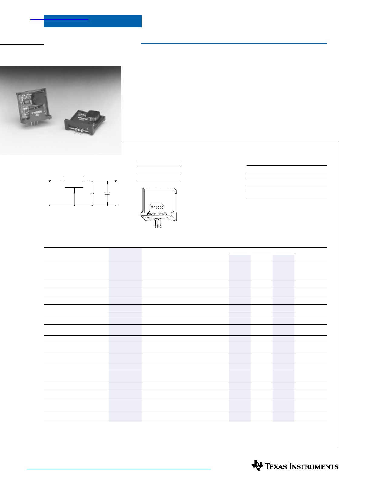
Standard Application
+V
in
1
COM
C1 = Optional ceramic (1-5µF)
C2 = Required Electrolytic (100µF)
PT5020
2
3
C
2
C
1
100µF
+
–V
COM
SLTS025B
(Revised 12/19/2001)
Features
• Negative Output
• Input Voltage Range:
+4.75 to +7 Volts
• Laser-Trimmed
• Small Footprint
• Soft Start
• 5-Pin Mount Option
(Suffixes L & M)
Pin-Out Information
Pin Function
1V
in
2 GND
out
3V
out
Ordering Information
PT5021 o = -3.3 Volts
PT5022 o = -5 Volts
PT5023 o = -9 Volts
PT5024 o = -12 Volts
PT5025 o = -15 Volts
PT5026 o = -5.2 Volts
PT5027 o = -8.0 Volts
PT5028 o = -6.5 Volts
PT5029 o = -5.5 Volts
PT5030 o = -6.0 Volts
PT5031 o = -1.7 Volts
Description
The PT5020 series of integrated
switching regulators (ISRs) convert a
positive input voltage, typically +5V, to a
negative output voltage for a wide range of
analog and datacom applications.
These Plus to Minus ISRs incorporate
a “Buck-Boost” topology and are packaged
in the 3-pin, single in-line pin (SIP)
package configuration.
PT Series Suffix
Case/Pin Order Package
Configuration Suffix Code *
Vertical N (EAD)
Horizontal A (EAA)
SMD C (EAC)
Horizontal, 2-pin Tab M (EAM)
SMD, 2-Pin Tab L (EAL)
* Previously known as package styles 100/110.
(Reference the applicable package code drawing
for the dimensions and PC board layout)
NOTE: PT5020 ISRs are not Short-Circuit Protected.
(PT1234x )
Specifications (Unless otherwise stated, T
=25°C, Vin =5V, Io =Iomax, C2 =100µF)
a
PT5020 SERIES
Characteristics Symbol Conditions Min Typ Max Units
Output Current I
Input Voltage Range V
Output Voltage Tolerance ∆V
Line Regulation Reg
Load Regulation Reg
o
in
o
line
load
Efficiency η I
Vo Ripple (pk-pk) V
Transient Response t
Current Limit I
Inrush Current I
Switching Frequency ƒ
Operating Temperature Range T
Thermal Resistance
Storage Temperature T
r
tr
lim
ir
t
ir
s
a
θ
ja
s
Mechanical Shock Per Mil-STD-883D, Method 2002.3
Mechanical Vibration Suffixes N, A, & C — 5 —
Per Mil-STD-883D, 20-2000 Hz Suffixes L & M — 20 —
Weight Suffixes N, A, & C — 4.5 —
Over Vin range Vo= –1.7V to –6.5V 0.25
= –9V 0.10
V
o
= –12V 0.10
V
o
Vo= –15V 0.10
Over Io range 4.75 — 7
Over Vin Range
Ta = -20°C to SOA limit
(3)
Over Vin range — ±0.5 ±1 %V
I
min ≤ Io ≤ I
o
=0.5 Iomax — 75 — %
o
max — ±0.5 ±1 %V
o
20MHz bandwidth — ±2 ±5 %V
25% load change — 500 — µSec
Vo over/undershoot — 3.0 5.0 %V
On start up — 1.0
Over I
range Vo =1.7 to 8V 0.8 1 1.2 MHz
o
Vo ≥8 V 500 650 800 kHz
— -20 — +85
Free Air Convection — 50 — °C/W
(40-60LFM)
1 msec, Half Sine, mounted to a fixture
Suffixes L & M — 6.5
(1)
— 1.0
(1)
—0.60
(1)
—0.50
(1)
—0.30
(2)
— ±1.5 ±3 %V
—150— %I
(3)
— 1.0 — mSec
—A
(4)
-40 — +125 °C
— 500 — G’s
(5)
—
Notes: (1) The ISR will operate at no load with reduced specifications.
(2) For applications with input voltages greater than 7 VDC, use the PT78NR100 Series.
(3) The inrush current stated is above the normal input current for the associated output load.
(4) See Safe Operating Area curves or consult the factory for the appropriate derating
(5) The tab pins on the 5-pin mount package types (suffixes L & M) must be soldered. For more information see the applicable package outline drawing.
A
V
o
°C
G’s
grams
o
o
o
o
o
max
For technical support and more information, see inside back cover or visit www.ti.com
PT5020 Series
Positive Input/Negative Output
Integrated Switching Regulator
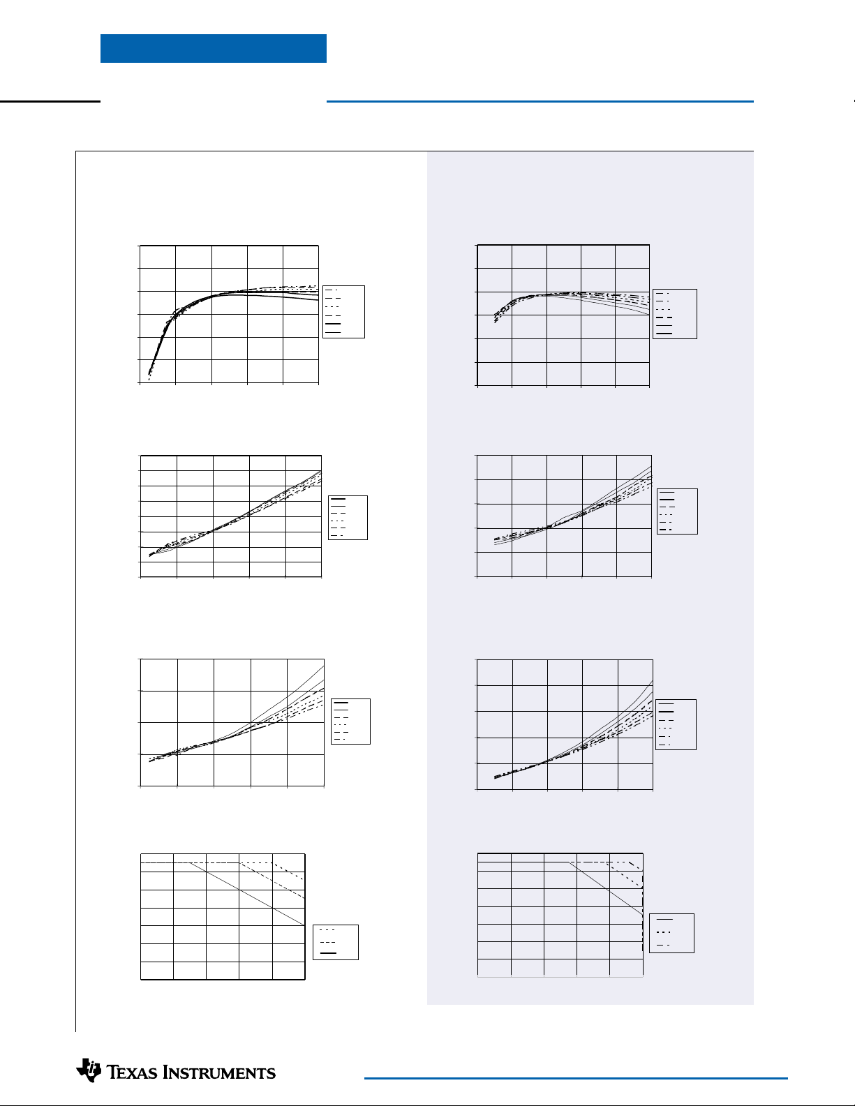
T ypical Characteristics
PT5024 (-12VDC) (See Note A)
Efficiency vs Output Current
100
90
80
70
Efficiency - %
60
50
40
0 0.1 0.2 0.3 0 .4 0 .5
Iout-(Amps)
Ripple Voltage vs Output Current
160
140
120
100
80
Ripple-(mV)
60
40
20
0
0 0.1 0.2 0.3 0.4 0.5
Vin
7.0V
6.5V
6.0V
5.5V
5.0V
4.75V
Vin
4.75V
5.0V
5.5V
6.0V
6.5V
7.0V
PT5022 (-5VDC) (See Note A)
Efficiency vs Output Current
100
90
80
70
Efficiency - %Ripple-(mV)PD-(Watts)
60
50
40
0 0 .2 0.4 0.6 0.8 1
Iout-(Amps)
Ripple Voltage vs Output Current
100
80
60
40
20
0
0 0.2 0 .4 0 .6 0 .8 1
Iout-(Amps)Iout-(Amps)
Vin
7.0V
6.5V
6.0V
5.5V
5.0V
4.75V
Vin
4.75V
5.0V
5.5V
6.0V
6.5V
7.0V
Power Dissipation vs Output Current
2
1.5
1
PD-(Watts)
0.5
0
0 0.1 0.2 0.3 0.4 0.5
Iout-(Amps)
Safe Operating Area (VIN=5V) (See Note B)
90
80
70
60
50
40
30
Ambient Temperature - (C°)
20
0.0 0.1 0.2 0.3 0.4 0.5
Airflow
90 LFM
60 LFM
0 LFM
Vin
4.75V
5.0V
5.5V
6.0V
6.5V
7.0V
Power Dissipation vs Output Current
2.5
2
1.5
1
0.5
0
0 0.2 0.4 0.6 0.8 1
Iout-(Amps)
Safe Operating Area (VIN=5V) (See Note B)
90
80
70
60
50
40
30
Ambient Temperature - (C°)
20
0 0.2 0.4 0.6 0.8 1
Maximum Output Current - (Amps)Maximum Output Current - (Amps)
Note A: Characteristic data has been developed from actual products tested at 25°C. This data is considered typical data for the Converter.
Note B: Thermal derating graphs are developed in free-air convection cooling, which corresponds to approximately 40–60LFM of airflow.
Vin
Airfl ow
0 LFM
60 LFM
90 LFM
4.75V
5.0V
5.5V
6.0V
6.5V
7.0V
For technical support and more information, see inside back cover or visit www.ti.com

PACKAGE OPTION ADDENDUM
www.ti.com
PACKAGING INFORMATION
Orderable Device Status
PT5021A ACTIVE SIP MOD
PT5021C ACTIVE SIP MOD
PT5021J ACTIVE SIP MOD
PT5021L ACTIVE SIP MOD
PT5021N ACTIVE SIP MOD
PT5022A ACTIVE SIP MOD
PT5022C ACTIVE SIP MOD
PT5022CT ACTIVE SIP MOD
PT5022H ACTIVE SIP MOD
PT5022J ACTIVE SIP MOD
PT5022L ACTIVE SIP MOD
PT5022M ACTIVE SIP MOD
PT5022N ACTIVE SIP MOD
PT5022S ACTIVE SIP MOD
PT5023A ACTIVE SIP MOD
PT5023C ACTIVE SIP MOD
PT5023N ACTIVE SIP MOD
PT5024A ACTIVE SIP MOD
PT5024C ACTIVE SIP MOD
PT5024CT ACTIVE SIP MOD
PT5024J ACTIVE SIP MOD
PT5024L ACTIVE SIP MOD
PT5024M ACTIVE SIP MOD
PT5024N ACTIVE SIP MOD
PT5024S ACTIVE SIP MOD
(1)
Package
Type
ULE
ULE
ULE
ULE
ULE
ULE
ULE
ULE
ULE
ULE
ULE
ULE
ULE
ULE
ULE
ULE
ULE
ULE
ULE
ULE
ULE
ULE
ULE
ULE
ULE
13-Oct-2005
Package
Drawing
EAA 3 35 TBD Call TI Level-1-215C-UNLIM
EAC 3 35 TBD Call TI Level-1-215C-UNLIM
EAJ 3 16 TBD Call TI Level-1-215C-UNLIM
EAL 3 35 TBD Call TI Level-1-215C-UNLIM
EAD 3 35 TBD Call TI Level-1-215C-UNLIM
EAA 3 35 TBD Call TI Level-1-215C-UNLIM
EAC 3 35 TBD Call TI Level-1-215C-UNLIM
EAC 3 200 TBD Call TI Level-1-215C-UNLIM
EAH 3 16 TBD Call TI Level-1-215C-UNLIM
EAJ 3 16 TBD Call TI Level-1-215C-UNLIM
EAL 3 35 TBD Call TI Level-1-215C-UNLIM
EAM 3 35 TBD Call TI Level-1-215C-UNLIM
EAD 3 35 TBD Call TI Level-1-215C-UNLIM
EAF 3 16 TBD Call TI Level-1-215C-UNLIM
EAA 3 35 TBD Call TI Level-1-215C-UNLIM
EAC 3 35 TBD Call TI Level-1-215C-UNLIM
EAD 3 35 TBD Call TI Level-1-215C-UNLIM
EAA 3 35 TBD Call TI Level-1-215C-UNLIM
EAC 3 35 TBD Call TI Level-1-215C-UNLIM
EAC 3 200 TBD Call TI Level-1-215C-UNLIM
EAJ 3 16 TBD Call TI Level-1-215C-UNLIM
EAL 3 35 TBD Call TI Level-1-215C-UNLIM
EAM 3 35 TBD Call TI Level-1-215C-UNLIM
EAD 3 35 TBD Call TI Level-1-215C-UNLIM
EAF 3 16 TBD Call TI Level-1-215C-UNLIM
Pins Package
Qty
Eco Plan
(2)
Lead/Ball Finish MSL Peak Temp
(3)
Addendum-Page 1

PACKAGE OPTION ADDENDUM
www.ti.com
Orderable Device Status
(1)
PT5025A ACTIVE SIP MOD
PT5025C ACTIVE SIP MOD
PT5025H ACTIVE SIP MOD
PT5025L ACTIVE SIP MOD
PT5025N ACTIVE SIP MOD
PT5026A ACTIVE SIP MOD
PT5026C ACTIVE SIP MOD
PT5026CT ACTIVE SIP MOD
PT5026H ACTIVE SIP MOD
PT5026J ACTIVE SIP MOD
PT5026L ACTIVE SIP MOD
PT5026LT ACTIVE SIP MOD
PT5026M ACTIVE SIP MOD
PT5026N ACTIVE SIP MOD
PT5027A ACTIVE SIP MOD
PT5027C ACTIVE SIP MOD
PT5027N ACTIVE SIP MOD
PT5028A ACTIVE SIP MOD
PT5028N ACTIVE SIP MOD
PT5029A ACTIVE SIP MOD
PT5029C ACTIVE SIP MOD
PT5029M ACTIVE SIP MOD
PT5030A ACTIVE SIP MOD
PT5030C ACTIVE SIP MOD
PT5030L ACTIVE SIP MOD
PT5030N ACTIVE SIP MOD
Package
Type
ULE
ULE
ULE
ULE
ULE
ULE
ULE
ULE
ULE
ULE
ULE
ULE
ULE
ULE
ULE
ULE
ULE
ULE
ULE
ULE
ULE
ULE
ULE
ULE
ULE
ULE
13-Oct-2005
Package
Drawing
Pins Package
Qty
Eco Plan
(2)
Lead/Ball Finish MSL Peak Temp
EAA 3 35 TBD Call TI Level-1-215C-UNLIM
EAC 3 35 TBD Call TI Level-1-215C-UNLIM
EAH 3 16 TBD Call TI Level-1-215C-UNLIM
EAL 3 35 TBD Call TI Level-1-215C-UNLIM
EAD 3 35 TBD Call TI Level-1-215C-UNLIM
EAA 3 35 TBD Call TI Level-1-215C-UNLIM
EAC 3 35 TBD Call TI Level-1-215C-UNLIM
EAC 3 200 TBD Call TI Level-1-215C-UNLIM
EAH 3 16 TBD Call TI Level-1-215C-UNLIM
EAJ 3 16 TBD Call TI Level-1-215C-UNLIM
EAL 3 35 TBD Call TI Level-1-215C-UNLIM
EAL 3 200 TBD Call TI Level-1-215C-UNLIM
EAM 3 35 TBD Call TI Level-1-215C-UNLIM
EAD 3 35 TBD Call TI Level-1-215C-UNLIM
EAA 3 35 TBD Call TI Level-1-215C-UNLIM
EAC 3 35 TBD Call TI Level-1-215C-UNLIM
EAD 3 35 TBD Call TI Level-1-215C-UNLIM
EAA 3 35 TBD Call TI Level-1-215C-UNLIM
EAD 3 35 TBD Call TI Level-1-215C-UNLIM
EAA 3 35 TBD Call TI Level-1-215C-UNLIM
EAC 3 35 TBD Call TI Level-1-215C-UNLIM
EAM 3 35 TBD Call TI Level-1-215C-UNLIM
EAA 3 35 TBD Call TI Level-1-215C-UNLIM
EAC 3 35 TBD Call TI Level-1-215C-UNLIM
EAL 3 35 TBD Call TI Level-1-215C-UNLIM
EAD 3 35 TBD Call TI Level-1-215C-UNLIM
(3)
Addendum-Page 2

PACKAGE OPTION ADDENDUM
www.ti.com
Orderable Device Status
(1)
PT5031C ACTIVE SIP MOD
Package
Type
Package
Drawing
Pins Package
Qty
Eco Plan
(2)
Lead/Ball Finish MSL Peak Temp
EAC 3 35 TBD Call TI Level-1-215C-UNLIM
13-Oct-2005
(3)
ULE
PT5031L ACTIVE SIP MOD
EAL 3 35 TBD Call TI Level-1-215C-UNLIM
ULE
PT5031N ACTIVE SIP MOD
EAD 3 35 TBD Call TI Level-1-215C-UNLIM
ULE
(1)
The marketing status values are defined as follows:
ACTIVE: Product device recommended for new designs.
LIFEBUY: TI has announced that the device will be discontinued, and a lifetime-buy period is in effect.
NRND: Not recommended for new designs. Device is in production to support existing customers, but TI does not recommend using this part in
a new design.
PREVIEW: Device has been announced but is not in production. Samples may or may not be available.
OBSOLETE: TI has discontinued the production of the device.
(2)
Eco Plan - The planned eco-friendly classification: Pb-Free (RoHS) or Green (RoHS & no Sb/Br) - please check
http://www.ti.com/productcontent for the latest availability information and additional product content details.
TBD: The Pb-Free/Green conversion plan has not been defined.
Pb-Free (RoHS): TI's terms "Lead-Free" or "Pb-Free" mean semiconductor products that are compatible with the current RoHS requirements
for all 6 substances, including the requirement that lead not exceed 0.1% by weight in homogeneous materials. Where designed to be soldered
at high temperatures, TI Pb-Free products are suitable for use in specified lead-free processes.
Green (RoHS & no Sb/Br): TI defines "Green" to mean Pb-Free (RoHS compatible), and free of Bromine (Br) and Antimony (Sb) based flame
retardants (Br or Sb do not exceed 0.1% by weight in homogeneous material)
(3)
MSL, Peak Temp. -- The Moisture Sensitivity Level rating according to the JEDEC industry standard classifications, and peak solder
temperature.
Important Information and Disclaimer:The information provided on this page represents TI's knowledge and belief as of the date that it is
provided. TI bases its knowledge and belief on information provided by third parties, and makes no representation or warranty as to the
accuracy of such information. Efforts are underway to better integrate information from third parties. TI has taken and continues to take
reasonable steps to provide representative and accurate information but may not have conducted destructive testing or chemical analysis on
incoming materials and chemicals. TI and TI suppliers consider certain information to be proprietary, and thus CAS numbers and other limited
information may not be available for release.
In no event shall TI's liability arising out of such information exceed the total purchase price of the TI part(s) at issue in this document sold by TI
to Customer on an annual basis.
Addendum-Page 3

IMPORTANT NOTICE
Texas Instruments Incorporated and its subsidiaries (TI) reserve the right to make corrections, modifications,
enhancements, improvements, and other changes to its products and services at any time and to discontinue
any product or service without notice. Customers should obtain the latest relevant information before placing
orders and should verify that such information is current and complete. All products are sold subject to TI’s terms
and conditions of sale supplied at the time of order acknowledgment.
TI warrants performance of its hardware products to the specifications applicable at the time of sale in
accordance with TI’s standard warranty. Testing and other quality control techniques are used to the extent TI
deems necessary to support this warranty . Except where mandated by government requirements, testing of all
parameters of each product is not necessarily performed.
TI assumes no liability for applications assistance or customer product design. Customers are responsible for
their products and applications using TI components. To minimize the risks associated with customer products
and applications, customers should provide adequate design and operating safeguards.
TI does not warrant or represent that any license, either express or implied, is granted under any TI patent right,
copyright, mask work right, or other TI intellectual property right relating to any combination, machine, or process
in which TI products or services are used. Information published by TI regarding third-party products or services
does not constitute a license from TI to use such products or services or a warranty or endorsement thereof.
Use of such information may require a license from a third party under the patents or other intellectual property
of the third party, or a license from TI under the patents or other intellectual property of TI.
Reproduction of information in TI data books or data sheets is permissible only if reproduction is without
alteration and is accompanied by all associated warranties, conditions, limitations, and notices. Reproduction
of this information with alteration is an unfair and deceptive business practice. TI is not responsible or liable for
such altered documentation.
Resale of TI products or services with statements different from or beyond the parameters stated by TI for that
product or service voids all express and any implied warranties for the associated TI product or service and
is an unfair and deceptive business practice. TI is not responsible or liable for any such statements.
Following are URLs where you can obtain information on other Texas Instruments products and application
solutions:
Products Applications
Amplifiers amplifier.ti.com Audio www.ti.com/audio
Data Converters dataconverter.ti.com Automotive www.ti.com/automotive
DSP dsp.ti.com Broadband www.ti.com/broadband
Interface interface.ti.com Digital Control www.ti.com/digitalcontrol
Logic logic.ti.com Military www.ti.com/military
Power Mgmt power.ti.com Optical Networking www.ti.com/opticalnetwork
Microcontrollers microcontroller.ti.com Security www.ti.com/security
Telephony www.ti.com/telephony
Video & Imaging www.ti.com/video
Wireless www.ti.com/wireless
Mailing Address: Texas Instruments
Post Office Box 655303 Dallas, Texas 75265
Copyright 2005, Texas Instruments Incorporated
 Loading...