

Page 1
Universal Operational Amplifier
Single, Dual, Quad (SOIC)
Evaluation Module
With Shutdown
User’s Guide
April 2001 Mixed-Signal Products
SLOU061A
Page 2

IMPORTANT NOTICE
T exas Instruments and its subsidiaries (TI) reserve the right to make changes to their products or to discontinue
any product or service without notice, and advise customers to obtain the latest version of relevant information
to verify, before placing orders, that information being relied on is current and complete. All products are sold
subject to the terms and conditions of sale supplied at the time of order acknowledgment, including those
pertaining to warranty, patent infringement, and limitation of liability.
TI warrants performance of its products to the specifications applicable at the time of sale in accordance with
TI’s standard warranty . T esting and other quality control techniques are utilized to the extent TI deems necessary
to support this warranty . Specific testing of all parameters of each device is not necessarily performed, except
those mandated by government requirements.
Customers are responsible for their applications using TI components.
In order to minimize risks associated with the customer’s applications, adequate design and operating
safeguards must be provided by the customer to minimize inherent or procedural hazards.
TI assumes no liability for applications assistance or customer product design. TI does not warrant or represent
that any license, either express or implied, is granted under any patent right, copyright, mask work right, or other
intellectual property right of TI covering or relating to any combination, machine, or process in which such
products or services might be or are used. TI’s publication of information regarding any third party’s products
or services does not constitute TI’s approval, license, warranty or endorsement thereof.
Reproduction of information in TI data books or data sheets is permissible only if reproduction is without
alteration and is accompanied by all associated warranties, conditions, limitations and notices. Representation
or reproduction of this information with alteration voids all warranties provided for an associated TI product or
service, is an unfair and deceptive business practice, and TI is not responsible nor liable for any such use.
Resale of TI’s products or services with statements different from or beyond the parameters
that product or service voids all express and any implied warranties for the associated TI product or service,
is an unfair and deceptive business practice, and TI is not responsible nor liable for any such use.
Also see: Standard Terms and Conditions of Sale for Semiconductor Products.
Mailing Address:
Texas Instruments
Post Office Box 655303
Dallas, Texas 75265
Copyright 2001, Texas Instruments Incorporated
www.ti.com/sc/docs/stdterms.htm
stated by TI for
Page 3

Related Documentation From Texas Instruments
J
Amplifiers and Comparators Data Book (literature number
SLOD002). This data book contains data sheets and other
information on the TI operational amplifiers that can be used with this
evaluation module.
J
Power Supply Circuits Data Book (literature number SLVD002).
This data book contains data sheets and other information on the TI
shunt regulators that can be used with this evaluation module.
FCC Warning
This equipment is intended for use in a laboratory test environment only. It
generates, uses, and can radiate radio frequency energy and has not been
tested for compliance with the limits of computing devices pursuant to subpart
J of part 15 of FCC rules, which are designed to provide reasonable protection
against radio frequency interference. Operation of this equipment in other
environments may cause interference with radio communications, in which
case the user at his own expense will be required to take whatever measures
may be required to correct this interference.
Preface
Trademarks
PowerPAD is a trademark of Texas Instruments.
Chapter Title—Attribute Reference
iii
Page 4

iv
Page 5

Running Title—Attribute Reference
Contents
1 Introduction 1-1. . . . . . . . . . . . . . . . . . . . . . . . . . . . . . . . . . . . . . . . . . . . . . . . . . . . . . . . . . . . . . . . . . . . .
1.1 Design Features 1-2. . . . . . . . . . . . . . . . . . . . . . . . . . . . . . . . . . . . . . . . . . . . . . . . . . . . . . . . . . . .
1.2 Power Requirements 1-2. . . . . . . . . . . . . . . . . . . . . . . . . . . . . . . . . . . . . . . . . . . . . . . . . . . . . . . .
2 Evaluation Module Layout 2-1. . . . . . . . . . . . . . . . . . . . . . . . . . . . . . . . . . . . . . . . . . . . . . . . . . . . . . . .
2.1 Physical Considerations 2-2. . . . . . . . . . . . . . . . . . . . . . . . . . . . . . . . . . . . . . . . . . . . . . . . . . . . .
2.2 Area 100—Single Device SOIC 2-3. . . . . . . . . . . . . . . . . . . . . . . . . . . . . . . . . . . . . . . . . . . . . . .
2.3 Area 200—Dual Device SOIC 2-4. . . . . . . . . . . . . . . . . . . . . . . . . . . . . . . . . . . . . . . . . . . . . . .
2.4 Area 300—Quad Device SOIC 2-5. . . . . . . . . . . . . . . . . . . . . . . . . . . . . . . . . . . . . . . . . . . . . . .
2.5 General Power Dissipation Considerations 2-7. . . . . . . . . . . . . . . . . . . . . . . . . . . . . . . . . . . . .
2.6 EVM Component Placement 2-8. . . . . . . . . . . . . . . . . . . . . . . . . . . . . . . . . . . . . . . . . . . . . . . . .
2.7 EVM Board Layout 2-9. . . . . . . . . . . . . . . . . . . . . . . . . . . . . . . . . . . . . . . . . . . . . . . . . . . . . . . . . .
3 Example Circuits 3-1. . . . . . . . . . . . . . . . . . . . . . . . . . . . . . . . . . . . . . . . . . . . . . . . . . . . . . . . . . . . . . . .
3.1 Schematic Conventions 3-2. . . . . . . . . . . . . . . . . . . . . . . . . . . . . . . . . . . . . . . . . . . . . . . . . . . . .
3.2 Inverting Amplifier 3-2. . . . . . . . . . . . . . . . . . . . . . . . . . . . . . . . . . . . . . . . . . . . . . . . . . . . . . . . . .
3.3 Noninverting Amplifier 3-3. . . . . . . . . . . . . . . . . . . . . . . . . . . . . . . . . . . . . . . . . . . . . . . . . . . . . . .
3.4 Differential Amplifier 3-4. . . . . . . . . . . . . . . . . . . . . . . . . . . . . . . . . . . . . . . . . . . . . . . . . . . . . . . . .
3.5 Sallen-Key Low-Pass Filter 3-5. . . . . . . . . . . . . . . . . . . . . . . . . . . . . . . . . . . . . . . . . . . . . . . . . .
3.6 Sallen-Key High-Pass Filter 3-6. . . . . . . . . . . . . . . . . . . . . . . . . . . . . . . . . . . . . . . . . . . . . . . . . .
3.7 Two Operational Amplifier Instrumentation Amplifier 3-8. . . . . . . . . . . . . . . . . . . . . . . . . . . . .
3.8 Quad Operational Amplifier Instrumentation Amplifier 3-10. . . . . . . . . . . . . . . . . . . . . . . . . . .
Chapter Title—Attribute Reference
v
Page 6

Running Title—Attribute Reference
Figures
2–1 Area 100 Schematic—Single Device, SOIC (8-pin) 2-3. . . . . . . . . . . . . . . . . . . . . . . . . . . . . . . .
2–2 Area 200 Schematic—Dual Device, SOIC (14-pin) 2-4. . . . . . . . . . . . . . . . . . . . . . . . . . . . . . . . .
2–3 Area 300 Schematic—Quad Device, SOIC (16-pin) 2-6. . . . . . . . . . . . . . . . . . . . . . . . . . . . . . . .
2–4 Maximum Power Dissipation vs Free-Air Temperature 2-7. . . . . . . . . . . . . . . . . . . . . . . . . . . . .
2–5 EVM Component Placement 2-8. . . . . . . . . . . . . . . . . . . . . . . . . . . . . . . . . . . . . . . . . . . . . . . . . . . .
2–6 EVM Board Layout—Top 2-9. . . . . . . . . . . . . . . . . . . . . . . . . . . . . . . . . . . . . . . . . . . . . . . . . . . . . . .
2–7 EVM Board Layout—Bottom 2-10. . . . . . . . . . . . . . . . . . . . . . . . . . . . . . . . . . . . . . . . . . . . . . . . . . .
3–1 Inverting Amplifier with Dual Supply Using Area 100 3-2. . . . . . . . . . . . . . . . . . . . . . . . . . . . . . .
3–2 Noninverting Amplifier with Single Supply Using Area 100 3-3. . . . . . . . . . . . . . . . . . . . . . . . . .
3–3 Single Operational Amplifier Differential Amplifier With Single Supply Using Area 100 3-4. .
3–4 Sallen-Key Low-Pass Filter With Dual Supply Using Area 200 3-5. . . . . . . . . . . . . . . . . . . . . . .
3–5 Sallen-Key High-Pass Filter With Single Supply Using Area 200 3-7. . . . . . . . . . . . . . . . . . . . .
3–6 Two Operational Amplifier Instrumentation Amplifier With Single Supply Using Area 200 3-9
3–7 Quad Operational Amplifier Instrumentation Amplifier With Dual Supply Using Area 300 3-11
Table
2–1 Dissipation Rating Table 2-7. . . . . . . . . . . . . . . . . . . . . . . . . . . . . . . . . . . . . . . . . . . . . . . . . . . . . . .
vi
Page 7

Chapter 1
Introduction
This user’s guide describes the universal operational amplifier single, dual,
quad (SOIC) evaluation module (EVM) with shutdown (SLOP248). The EVM
simplifies evaluation of Texas Instruments surface-mount op amps with or
without shutdown feature.
Topic Page
1.1 Design Features 1–2. . . . . . . . . . . . . . . . . . . . . . . . . . . . . . . . . . . . . . . . . . . . . .
1.2 Power Requirements 1–2. . . . . . . . . . . . . . . . . . . . . . . . . . . . . . . . . . . . . . . . . .
Introduction
1-1
Page 8

Design Features
1.1 Design Features
The EVM board design allows many circuits to be constructed easily and
quickly. There are three circuit development areas on the board, and each
uses IC amplifiers in the SOIC package. Area 100 is for a single operational
amplifier (op amp), with or without shutdown. It also features offset nulling pin
pads. Area 200 is for a dual op amp, with or without shutdown. Area 300 is for
a quad op amp, with or without shutdown. A few possible circuits include:
-
-
-
-
-
-
-
-
-
-
-
The EVM PCB is of two-layer construction, with a ground plane on the solder
side. Circuit performance should be comparable to final production designs.
Voltage follower
Noninverting amplifier
Inverting amplifier
Simple or algebraic summing amplifier
Difference amplifier
Current to voltage converter
Voltage to current converter
Integrator/low-pass filter
Differentiator/high-pass filter
Instrumentation amplifier
Sallen-Key filter
1.2 Power Requirements
The devices and designs that are used dictate the input power requirements.
Three input terminals are provided for each area of the board:
Vx+ Positive input power for area x00 i.e., V1+ ⇒ area 100
GNDx Ground reference for area x00 i.e., GND2 ⇒ area 200
Vx– Negative input power for area x00 i.e., V3– ⇒ area 300
Each area has four bypass capacitors – two for the positive supply, and two
for the negative supply . Each supply should have a 1-µF to 10-µF capacitor for
low-frequency bypassing and a 0.01-µF to 0.1-µF capacitor for high-frequency
bypassing.
When using single-supply circuits, the negative supply is shorted to ground by
bridging C104 or C105 in area 100, C209 or C210 in area 200, or C31 1 or C312
in area 300. Power input is between Vx+ and GNDx. The voltage reference
circuitry is provided for single-supply applications that require a reference
voltage to be generated.
1-2
Introduction
Page 9

Chapter 2
Evaluation Module Layout
This chapter shows the universal operational amplifier single, dual, quad
(SOIC) evaluation module (EVM) with shutdown board layout, schematics of
each area, and describes the relationships between the three areas.
Topic Page
2.1 Physical Considerations 2–2. . . . . . . . . . . . . . . . . . . . . . . . . . . . . . . . . . . . . . .
2.2 Area 100—Single Device SOIC 2–3. . . . . . . . . . . . . . . . . . . . . . . . . . . . . . . . .
2.3 Area 200—Dual Device SOIC 2–4. . . . . . . . . . . . . . . . . . . . . . . . . . . . . . . . . .
2.4 Area 300—Quad Device SOIC 2–5. . . . . . . . . . . . . . . . . . . . . . . . . . . . . . . . . .
2.5 General Power Dissipation Considerations 2–7. . . . . . . . . . . . . . . . . . . . . .
2.6 Component Placement 2–8. . . . . . . . . . . . . . . . . . . . . . . . . . . . . . . . . . . . . . . .
2.7 Board Layout 2–9. . . . . . . . . . . . . . . . . . . . . . . . . . . . . . . . . . . . . . . . . . . . . . . . .
Evaluation Module Layout
2-1
Page 10

Physical Considerations
2.1 Physical Considerations
The EVM board has three circuit development areas. Each area can be
separated from the others by breaking along the score lines. The circuit layout
in each area supports an op amp package, voltage reference, and ancillary
devices. The op amp package is unique to each area as described in the
following paragraphs. The voltage reference and supporting devices are the
same for all areas. Surface-mount or through-hole components can be used
for all capacitors and resistors on the board.
The voltage reference can be either surface-mount or through-hole. If
surface-mount is desired, the TL V431ACDBV5 or TLV431AIDBV5 adjustable
shunt regulators can be used. If through hole is desired, the TLV431ACLP,
TLV431AILP, TL431CLP, TL431ACLP, TL431ILP, or TL431AILP adjustable
shunt regulators can be used. Refer to Texas Instruments’ Power Supply
Circuits Data Book (literature number SLVD002) for details on usage of these
shunt regulators.
Each passive component (resistor or capacitor) has a surface mount 1206
footprint with through holes at 0.2″ spacing on the outside of the 1206 pads.
C105, C106, C107, C207, C208, C209, C312, C314, and C315 have a surface
mount 1210 footprint with through holes at 0.2″ spacing on the outside of the
1210 pads. Therefore, either surface-mount or through-hole parts can be
used. The potentiometer for the offset nulling feature in area 100 can also be
either a surface-mount or a through-hole unit.
Figures 2–1 through 2–3 show schematics for each of the board areas. The
schematics show all components that the board layout can accommodate.
These should only be used as reference, since not all components will be used
at any one time.
2-2
Evaluation Module Layout
Page 11

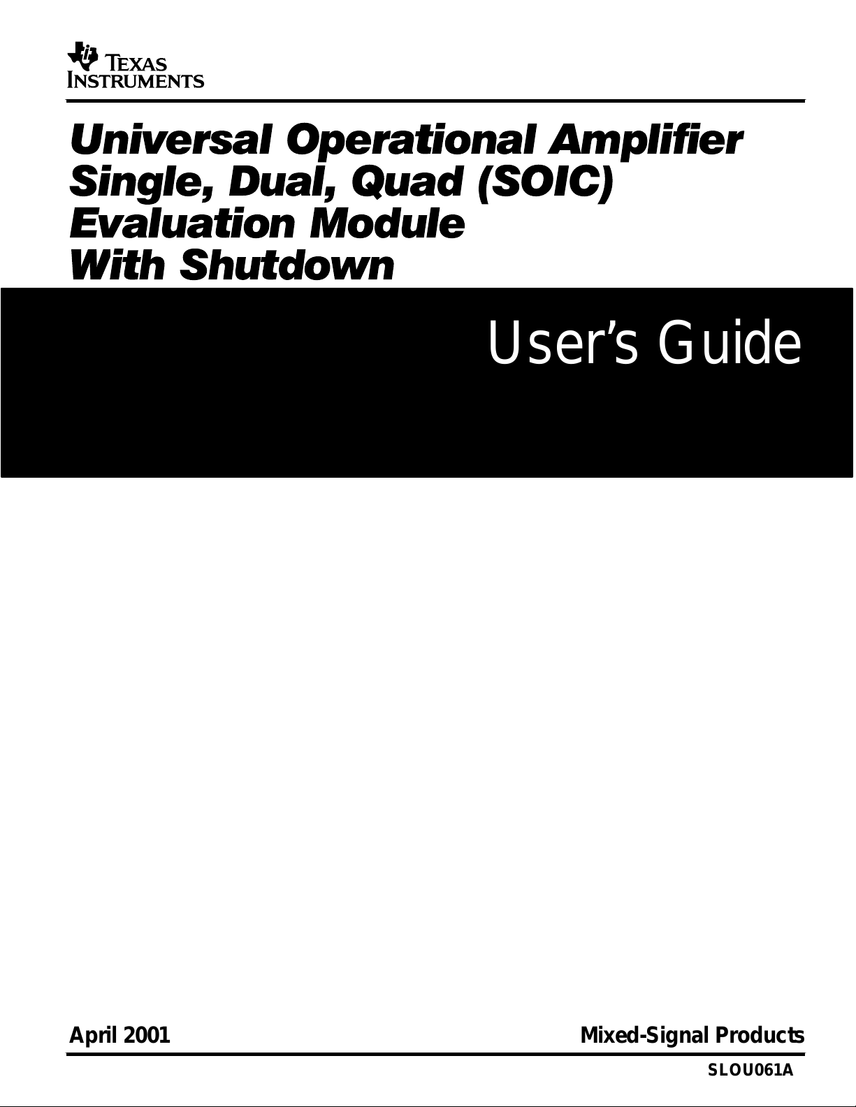
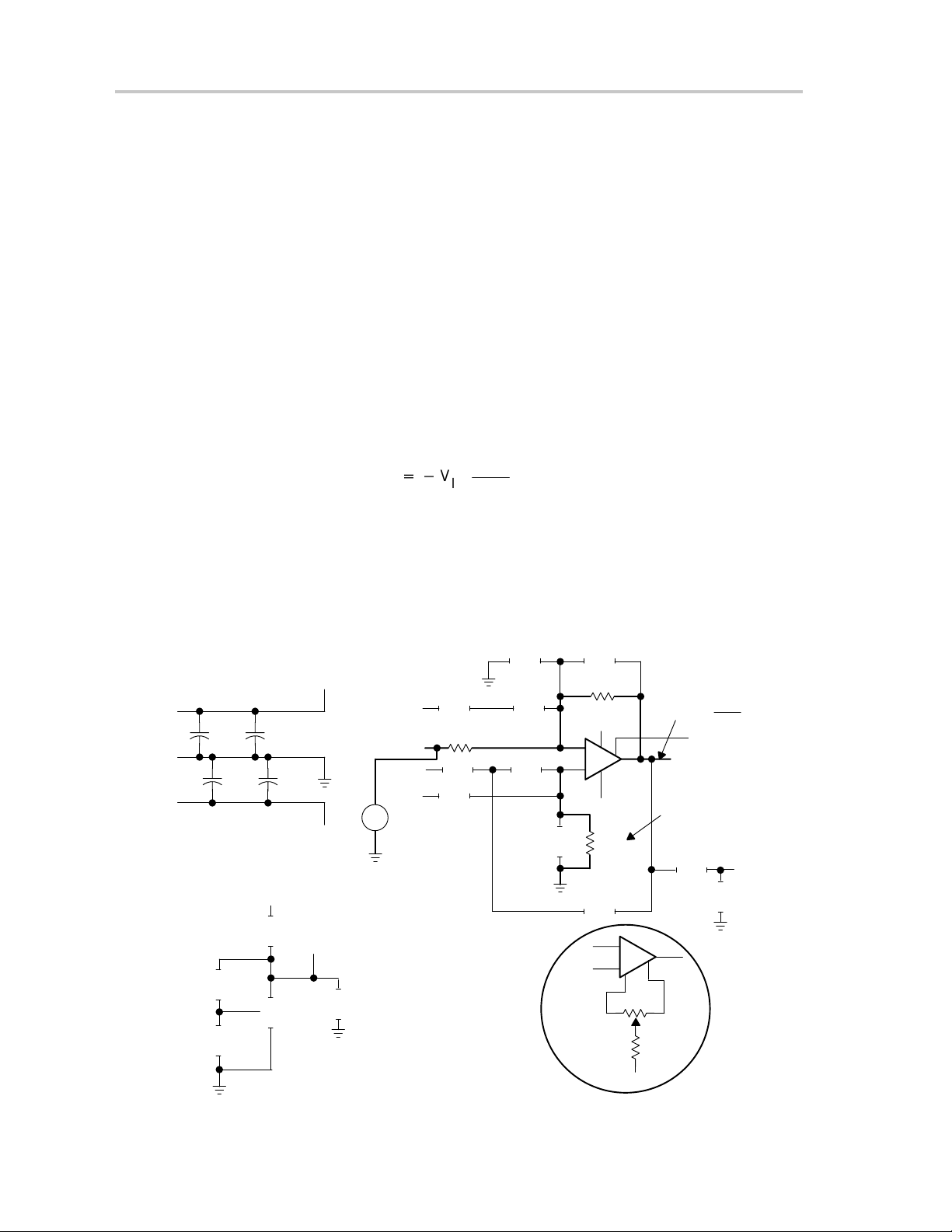
2.2 Area 100—Single Device SOIC
Area 100 uses 1xx reference designators, and is compatible with a single op
amp, with or without shutdown, packaged as an 8-pin SOIC. This
surface-mount package is designated by a D suffix in TI part numbers, as in
TxxxxCD, TxxxxID, etc.
Offset nulling can be extremely important in some applications. The EVM
accommodates TI IC op amps that provide this feature. The input offset can
be adjusted by connecting a 100-kΩ potentiometer between terminals 1 and
5 of the device and connecting the wiper to VCC– via a resistor (R101) as
shown below. This resistor is used to fine tune the offset adjustment. For
example, when using the TLC070 or TLC071 device and a 100-kΩ nulling
potentiometer, the of fset voltage adjustment is ±10 mV when R101 is 5.6 kΩ
and ±3 mV when R101 is 20 kΩ.
When using the nonshutdown version of the device, pin 8 of the IC is a no
connect.
Figure 2–1 shows the area 100 schematic.
Figure 2–1.Area 100 Schematic—Single Device, SOIC (8 pin)
V1+
R114
Physical Considerations
C110
V1+
C107 C108
GND1
C105 C104
V1–
Power Supply Bypass
V1+ VREF1
R108
U102
R111
R113
Voltage Reference
V1–
C106
A101–
A102–
A103+
A104+
C101
R110
R109
R103
R102
R105
C109
R104
C102
2
3
R101
1
R112
V1+
7
–
+
R107
V1–
8
4
V1–
U101
6
5
SD
OUT
R106
A1 FLT
C103
Evaluation Module Layout
2-3
Page 12
Physical Considerations
2.3 Area 200—Dual Device SOIC
Area 200 uses 2xx reference designators, and is compatible with dual op
amps, with or without shutdown, packaged as an 8-pin (without shutdown) or
14-pin (with shutdown) SOIC. This package is designated by a D suffix in TI
part numbers, as in TxxxxCD.
When using the nonshutdown version of the device, ensure that the IC is
aligned at the top of the IC pad array—the last six PCB pads (three on each
side—pins 5, 6, 7, 8, 9, and 10) will not be used.
Figure 2–2 shows the area 200 schematic.
Figure 2–2.Area 200 Schematic—Dual Device, SOIC (14 pin)
R216
C211
V2+
V2+
C206 C207
GND2
C209 C210
V2–
Power Supply Bypass
V2+ VREF2
R210
U202
R211
R213
Voltage Reference
V2–
C208
A201–
A202–
A203+
A204+
B201–
B202–
B203+
B204+
R221
R220
R219
R217
R204
R203
R201
R202
C215
R218
C212
R207
C202
R205
C204
R212
V2+
6
14
2
–
+
V2–
R215
C213
C203
R206
–
+
R209
U201a
4
9
U201b
1
13
3
12
11
A2/SD
A2OUT
1/2 Dual Op Amp
R214
B2/SD
B2OUT
1/2 Dual Op Amp
R208
A2 FLT
C214
B2 FLT
C205
2-4
C201
Evaluation Module Layout
Page 13

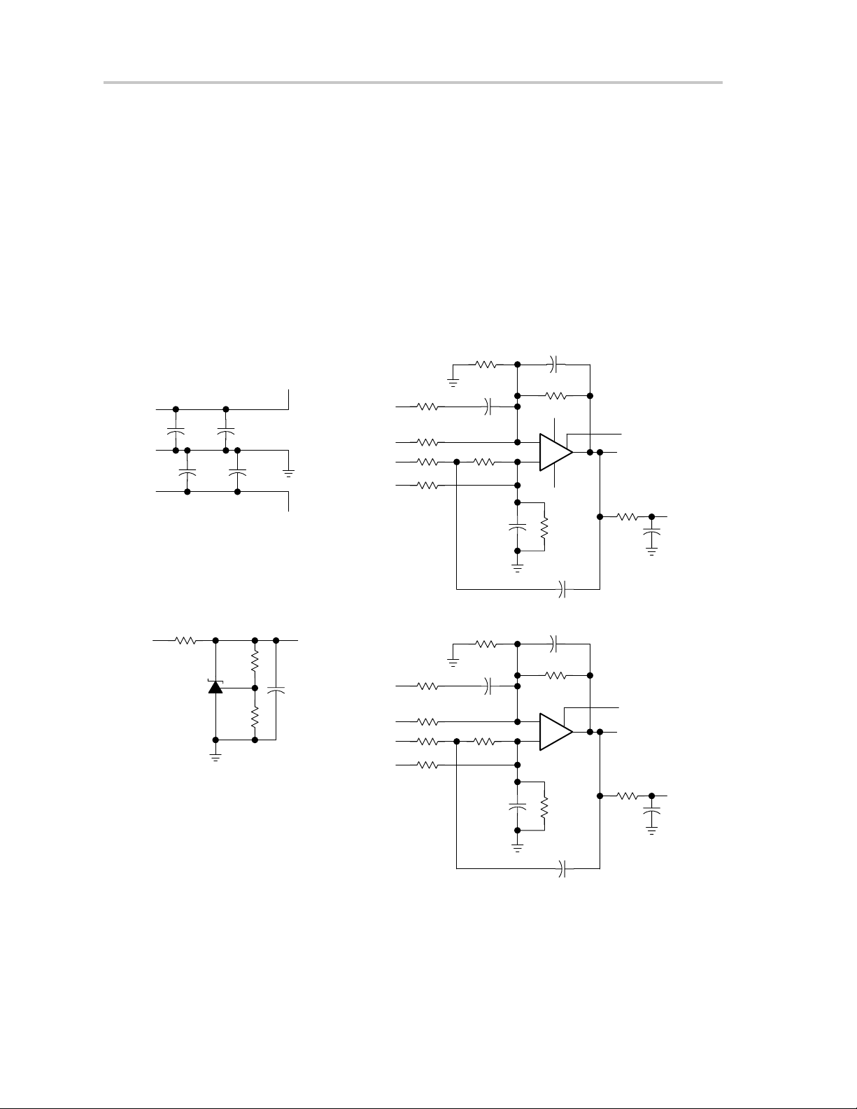
2.4 Area 300—Quad Device SOIC
Area 300 uses 3xx reference designators, and is compatible with quad op
amps, with or without shutdown, packaged in a 14-pin (without shutdown) or
16-pin (with shutdown) SOIC. This surface-mount package is designated by
a D suffix in TI part numbers, as in TxxxxID.
When using the nonshutdown version of the device, ensure that the IC is
aligned at the top of the IC pad array—the last two PCB pads (one on each
side—pins 8 and 9) will not be used.
Figure 2–3 shows the area 300 schematic.
Physical Considerations
Evaluation Module Layout
2-5
Page 14
Physical Considerations
Figure 2–3.Area 300 Schematic—Quad Device SOIC (16 pin)
B301–
B302–
B303+
B304+
V3+
GND3
V3–
Power Supply Bypass
R310
R312
R313
R315
C313 C314
C311 C312
R314
C308
R317
C307
V3+
A301–
A302–
V3–
C310
R318
6
–
+
7
U301B
R311
5
A303+
A304+
B3 OUT
R316
R301
R303
R306
R308
B3 FLT
C306
R304
C301
R305
C304
R323
2
3
C302
R302
V3+
4
–
+
V3–
R307
C303
C317
8
13
1
U301A
AB3/SD
A3 OUT
R309
A3 FLT
C305
D301–
D302–
D303+
D304+
R332
R333
R335
R336
R331
C321
R334
C322
C309
C301–
C302–
C324
R339
15
–
14
16
+
U301D
R337
C325
C303+
C304+
D3 OUT
R338
R322
R324
R327
R329
D3 FLT
C323
C316
R326
C318
V1+ VREF3
R325
11
9
–
+
R321
U302
10
U301C
R328
C319
12
CD3/SD
C3 OUT
R330
R320
C315
R319
Voltage Reference
C3 FLT
C320
2-6
Evaluation Module Layout
Page 15

General Power Dissipation Considerations
2.5 General Power Dissipation Considerations
For a given θJA, the maximum power dissipation is shown in Figure 2–4 and is calculated by the
following formula:
T
MAX–TA
ǒ
PD+
q
Where:
P
= Maximum power dissipation of Txxxx IC (watts)
D
T
= Absolute maximum junction temperature (150°C)
MAX
T
= Free-air temperature (°C)
A
θ
JA
= θ
JC
+ θ
θJC= Thermal coefficient from junction to case
θ
= Thermal coefficient from case to ambient air (°C/W)
CA
Figure 2–4.Maximum Power Dissipation vs Free-Air Temperature
2
1.5
Ǔ
JA
CA
MAXIMUM POWER DISSIPATION
vs
FREE-AIR TEMPERATURE
SOIC (16-pin)
Package
Low-K Test PCB
θJA = 114.7°C/W
TJ = 150°C
1
0.5
Maximum Power Dissipation – W
0
–55 –25 5
NOTE A: Results are with no air flow and using JEDEC Standard Low-K test PCB.
Table 2–1.Dissipation Rating Table
PACKAGE
D (8) 38.3 176 710 mW
D (14) 26.9 122.3 1022 mW
D (16) 25.7 114.7 1090 mW
SOIC (8-pin)
Package
Low-K Test PCB
SOIC (14-pin)
Package
Low-K Test PCB
35
TA – Free-Air Temperature – °C
θ
JC
(°C/W)
θ
JA
(°C/W)
65 95 125
TA ≤ 25°C
POWER RATING
Evaluation Module Layout
2-7
Page 16
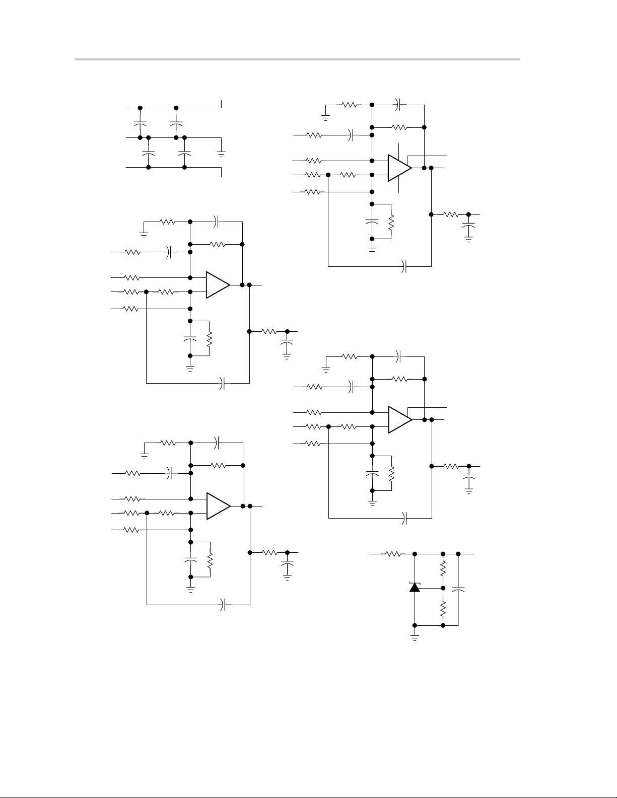
EVM Component Placement
2.6 EVM Component Placement
Figure 2–5 shows component placement for the EVM board.
Figure 2–5.EVM Component Placement
2-8
Evaluation Module Layout
Page 17

2.7 EVM Board Layout
Figures 2–6 and 2–7 show the EVM top and bottom board layouts,
respectively.
Figure 2–6.EVM Board Layout—Top
EVM Board Layout
Evaluation Module Layout
2-9
Page 18

EVM Board Layout
Figure 2–7.EVM Board Layout—Bottom
2-10
Evaluation Module Layout
Page 19

Chapter 3
Example Circuits
This chapter shows and discusses several example circuits that can be
constructed using the universal operational amplifier EVM. The circuits are all
classic designs that can be found in most operational amplifier design books.
Topic Page
3.1 Schematic Conventions 3–2. . . . . . . . . . . . . . . . . . . . . . . . . . . . . . . . . . . . . . .
3.2 Inverting Amplifier 3–2. . . . . . . . . . . . . . . . . . . . . . . . . . . . . . . . . . . . . . . . . . . .
3.3 Noninverting Amplifier 3–3. . . . . . . . . . . . . . . . . . . . . . . . . . . . . . . . . . . . . . . .
3.4 Differential Amplifier 3–4. . . . . . . . . . . . . . . . . . . . . . . . . . . . . . . . . . . . . . . . . .
3.5 Sallen-Key Low-Pass Filter 3–5. . . . . . . . . . . . . . . . . . . . . . . . . . . . . . . . . . . .
3.6 Sallen-Key High-Pass Filter 3–6. . . . . . . . . . . . . . . . . . . . . . . . . . . . . . . . . . . .
3.7 Two Operational Amplifier Instrumentation Amplifier 3–8. . . . . . . . . . . .
3.8 Quad Operational Amplifier Instrumentation Amplifier 3–10. . . . . . . . .
Example Circuits
3-1
Page 20
Schematic Conventions
3.1 Schematic Conventions
Figures 3–1 through 3–6 show schematic examples of circuits that can be
constructed using the universal operational amplifier EVM with shutdown. The
components that are placed on the board are shown in bold. Unused
components are blanked out. Jumpers and other changes are noted. These
examples are only a few of the many circuits that can be built.
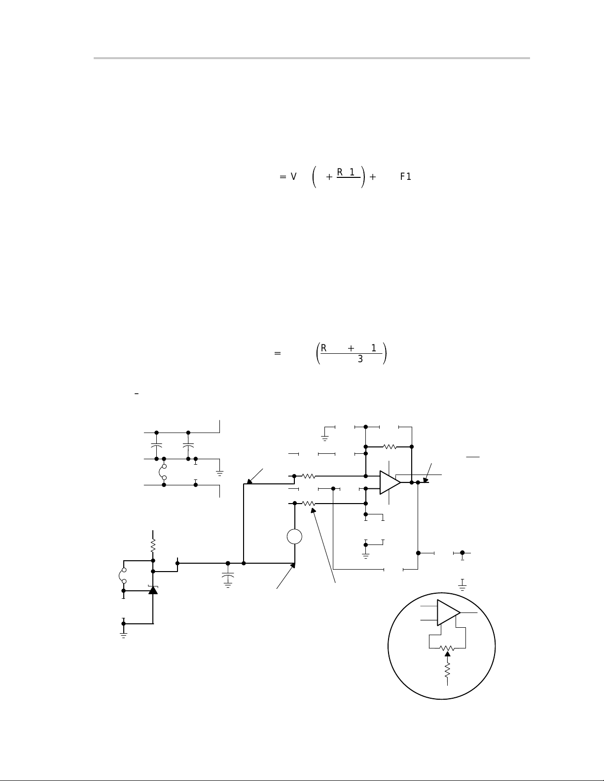
3.2 Inverting Amplifier
Figure 3–1 shows area 100 equipped with a single operational amplifier
configured as an inverting amplifier using dual power supplies.
Basic setup is done by choice of input and feedback resistors. The transfer
function for the circuit as shown is:
V
OUT
+*
R112
V
IN
R109
To cancel the effects of input bias current, set R105 = R112 || R109, or use a
0-Ω jumper for R105 if the operational amplifier is a low input bias operational
amplifier.
Figure 3–1.Inverting Amplifier With Dual Supply Using Area 100
C110
2
3
+
C102
V1+
GND1
V1–
Power Supply Bypass
C107 C108
0.1 µF 10 µF
C105 C104
0.1 µF 10 µF
V1+
V1+
V1–
A101–
A102–
A103+
A104–
+
V
–
R114
R110
R109
R103
R102
in
C109
R104
C101
R112
V1+
–
V1–
R105
7
4
8
6
U101
= –V
A OUT
R106
SD
IN
R112
R109
V
OUT
R105 = R112 II R109,
or Short if Using Low
Input Bias Op Amp
A1 FLT
C103
3-2
R108
R111
C
U102
R
A
R113
Voltage Reference
Not Used
VREF1
C106
Optional
2
3
R101
+
1
–
R107
V1–
6
5
100 k
5.6 k
Example Circuits
Page 21
3.3 Noninverting Amplifier
Figure 3–2 shows area 100 equipped with a single operational amplifier
configured as a noninverting amplifier with single-supply power input.
Basic setup is done by choice of input and feedback resistors. The transfer
function for the circuit as shown is:
The input signal must be referenced to VREF1.
To cancel the effects of input bias current, set R102 = R112 || R109, or use a
0-Ω jumper for R102 if the operational amplifier is a low input bias operational
amplifier.
The TL431 adjustable precision shunt regulator, configured as shown,
provides a low impedance reference for the circuit at about 1/2 V1+ in a 3 V
system. Another option is to adjust resistors R113 and R111 for the desired
VREF1 voltage. The formula for calculating VREF1 is:
V
OUT
+
Noninverting Amplifier
R112
ǒ
V
1
)
IN
R109
Ǔ
)
VREF1
VREF1+1.24 V
ǒ
R113
Ǔ
R111)R113
Figure 3–2.Noninverting Amplifier With Single Supply Using Area 100
V1+
GND1
V1–
R111
Jumper
R113
Voltage Reference
C107 C108
0.1 µF 10 µF
C105
Jumper
Power Supply Bypass
V1+
R108
2.2 kΩ
VREF1 = 1.24 V
C
U102 = TLV431ACDBV5
R
A
V1+
Jumper 102 – to VREF1
C104
V1–
C106
10 µF
Input Signal With
Reference to VREF1
A101+
A102–
A103+
A104–
+
–
R110
R109
R103
R102
V
in
R114
C109
R104
C101
R102 = R112 II R109,
or Short if Using Low Input
Bias Op Amp
2
3
C110
R112
V1+
7
–
+
4
V1–
R105
C102
Optional
8
6
U101
V
= V
()
OUT
IN
SD
1 OUT
R106
2
–
3
+
1
R107
R101
R112
1 + + VREF4
R109
1 FLT
C103
6
5
100 k
5.6 k
V1–
Example Circuits
3-3
Page 22

Differential Amplifier
3.4 Differential Amplifier
Figure 3–3 shows area 100 equipped with a single operational amplifier
configured as a differential amplifier using a voltage reference and single
power supply.
Basic setup is done by choice of input and feedback resistors. The transfer
function for the circuit as shown is:
Where:
The TLV431 adjustable precision shunt regulator, configured as shown,
provides a low impedance reference for the circuit at about 1/2 V1+ in a 3-V
system. Another option is to adjust resistors R111 and R113 for the desired
VREF1 voltage. The formula for calculating VREF1 is:
V
OUT
R112
R109
+
+
V
IN
R102
R103
ǒ
VREF1+1.24 V
R112
Ǔ
R109
)
R111)R113
ǒ
R113
VREF1
Ǔ
Figure 3–3.Single Operational Amplifier Differential Amplifier With Single Supply Using
Area 100
V1+
GND1
V1–
Jumper
Power Supply Bypass
C107 C108
0.1 µF 10 µF
C105
R111
R113
C104
V1+
R108
2.2 kΩ
VREF1 = 1.24 V
C
R
TLV431ACDBV5
A
Voltage Reference
U102
V1+
V1–
R114
101–
+
102–
V
in
103+
–
104+
C106
10 µF
R110
R109
R103
R102
Jumper 104+ to VREF1
C109
R104
Jumper
C101
C110
R112
R112
= V
in
()
R109
1/SD
1OUT
R112
=
R109
R106
R102
R103
+ V
A1 FLT
C103
REF1
4
8
6
U101
V
out
V1+
7
2
–
3
+
V1–
R105
C102
3-4
Example Circuits
Page 23
Sallen-Key Low-Pass Filter
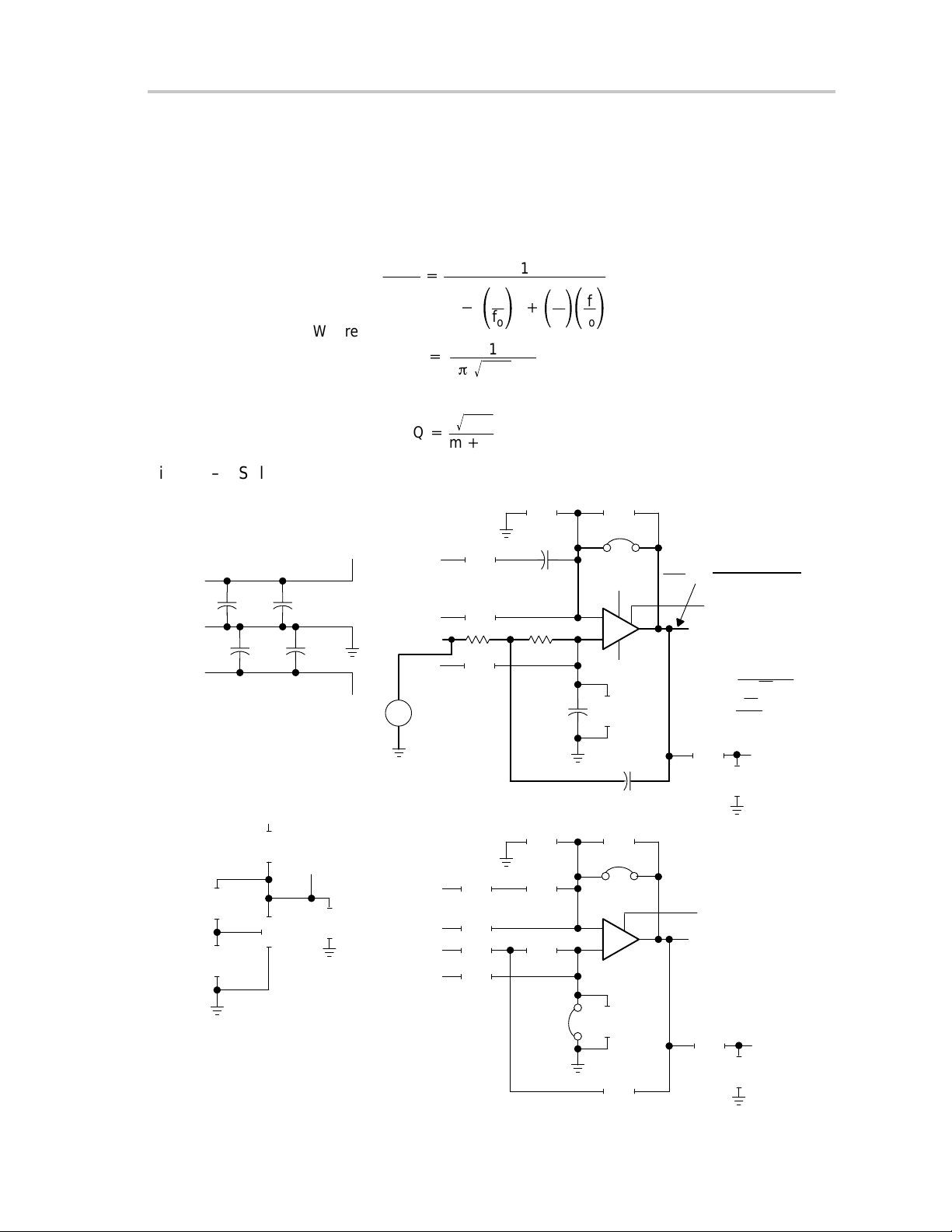
3.5 Sallen-Key Low-Pass Filter
Figure 3–4 shows area 200 equipped with a dual operational amplifier
configured as a second-order Sallen-Key low-pass filter using dual-power
supplies.
Basic setup is done by proper choice of resistors R and mR, and capacitors
C and nC. The transfer function is:
V
OUT
+
V
IN
1
*
Where:
fo+
2pmnǸRC
And
Ǹ
+
mn
m)1
Q
Figure 3–4.Sallen-Key Low-Pass Filter Wwith Dual Supply Using Area 200
1
2
)
j
f
ǒ
Ǔ
ǒ
Ǔ
f
Q
o
f
ǒ
Ǔ
f
o
1
R216
C211
V2+
GND2
V2–
Power Supply Bypass
R211
R213
C206 C207
0.1µF10µF
C209 C210
0.1µF10µF
V2+
R210
VREF2
C
U202
R
A
V2+
V2–
C208
A201–
A202–
A203+
A204+
+
V
in
–
B201–
B202–
B203+
B204+
R221
R220
R219
mR R
R217
R204
R203
R201
R202
C215
R218
C212
R207 C203
C202
R205
Jumper
2
3
Jumper
12
11
R212
V2+
14
–
+
V2–
C213
R206
–
+
V
out
=
1– (f/fo)
V
in
6
1
U201A
4
R215
nC
9 B2/SD
13
U201B
A2/SD
A2OUT
1/2 Dual Op Amp
fo =
Q =
R214
B2OUT
1/2 Dual Op Amp
Not Used
1
2
+ (j/Q)(f/fo)
1
2π √mn RC
√mn
m+1
A2 FLT
C214
Voltage Reference
Not Used
C204
Jumper
R209
C201
Example Circuits
R208
B2 FLT
C205
3-5
Page 24

Sallen-Key High-Pass Filter
3.6 Sallen-Key High-Pass Filter
Figure 3–5 shows area 200 equipped with a dual operational amplifier
configured as a second-order Sallen-Key high-pass filter using single-supply
power input.
Basic setup is done by proper choice of resistors R and mR, and capacitors
C and nC. Note that capacitors should be used for components R201 and
R205, and a resistor for C201. The transfer function for the circuit as shown
is:
ȡ
V
Where:
And
The TL431 adjustable precision shunt regulator, configured as shown,
provides a low impedance reference for the circuit at about 1/2 V2+ in a 5 V
system. Another option is to adjust resistors R211 and R213 for the desired
VREF2 voltage. The formula for calculating VREF2 is:
+
OUT
VREF2+2.50 V
V
f
+
o
Q
+
ȧ
ȧ
IN
ȧ
1
Ȣ
1
Ǹ
2pmn
Ǹ
mn
n)1
R211)R213
ǒ
)
RC
*
j
ǒ
Q
R213
Ǔ
ǒ
ǒ
f
2
f
Ǔ
f
o
f
Ǔ*ǒ
o
Ǔ
ȣ
ȧ
)
VREF2
ȧ
2
ȧ
f
Ǔ
f
Ȥ
o
3-6
Example Circuits
Page 25

Sallen-Key High-Pass Filter
Figure 3–5.Sallen-Key High-Pass Filter With Single Supply Using Area 200
R216 C211
V2+
C206 C207
GND2
V2–
Jumper
Voltage Reference
0.1 µF 10 µF
Jumper
Power Supply Bypass
V2+
R211
C
R
A
R213
V2+
C210
C209
V2–
VREF2 = 2.5 V
B201–
R210
2.2 kΩ
U202
TL431ACLP
Jumper B204 + to VREF2
C208
10 µF
B202–
B204+
B203+
A201–
A202–
A203+
A204+
R204
R203
R202
mR
R201
CnC
+
V
in
–
R221
R220
R219
R217
R207 C203
C202
R205
C204
C215
R218
C212
Jumper
12
11
R206
–
+
R209
C201
9
U201B
R
13
R212
Jumper
14
2
–
3
+
V2–
Jumper
C213
V
OUT
V2+
6
1
U201A
4
R215
= V
B2OUT
1/2 Dual Op Amp
R208
1/2 Dual Op Amp
Not Used
IN
1+(j/Q)(f/fo) – (f/fo)
B2/SD
fo =
Q =
A2/SD
A2OUT
R214
–(f/fo)
2π √mn
√mn
m+1
B2 FLT
C205
A2 FLT
C214
2
+ VREF2
2
1
RC
Example Circuits
3-7
Page 26

T wo Operational Amplifier Instrumentation Amplifier
3.7 Two Operational Amplifier Instrumentation Amplifier
Figure 3–6 shows area 200 equipped with a dual operational amplifier
configured as a two-operational-amplifier instrumentation amplifier using a
voltage reference and single power supply.
Basic setup is done by choice of input and feedback resistors. The transfer
function for the circuit as shown is:
2R212
ǒ
1
V
Where:
To cancel the effects of input bias current, set R217 = R212 || R220 and set
R202 = R206 ||R203, or use a 0-Ω jumper for R217 and R202 if the operational
amplifier is a low input bias operational amplifier.
The TLV431 adjustable precision shunt regulator, configured as shown,
provides a low impedance reference for the circuit at about 1/2 V2+ in a 3 V
system. Another option is to adjust resistors R211 and R213 for the desired
VREF2 voltage. The formula for calculating VREF2 is:
VREF2+1.24 V
+
OUT
R212 = R206 and R221 = R203
V
)
IN
R211)R213
ǒ
R220
R213
)
R212
R221
Ǔ
Ǔ
)
VREF2
3-8
Example Circuits
Page 27

T wo Operational Amplifier Instrumentation Amplifier
Figure 3–6.Two Operational Amplifier Instrumentation Amplifier Wwith Single Supply
Using
Area 200
or Short if Using Low Input
V2+
GND2
Jumper
V2–
Power Supply Bypass
V2+
R211
R213
C
R
A
Jumper
R217 = R212 II R220
Bias Op Amp
C206 C207
0.1 µF 10 µF
C209 C210
Jumper VREF2 to B202–
R210
2.2 kΩ
VREF2 = 1.24 V
U202
TLV431ACDBV5
V2+
V2–
C208
10 µF
A201–
A202–
A203+
A204+
Jumper
A202– to B201–
+
V
in
–
B201–
B202–
B203+
B204+
R204
R203
R201
R202
R221
R220
R219
R217
R216
C215
Jumper
R218
C212
R207
C202
JumperJumper
R205
C211
Jumper A201 – to B2OUT
R212
2R212
V
= V
(1+ + )+ V
OUT
V2+
14
6
2
–
1
3
+
U201A
4
V2–
R215
C213
C203
R206
9
12
–
11
13
+
U201B
in
A2/SD
A2OUT
1/2 Dual Op Amp
R212 = R206
R221 = R203
R214
B2/SD
B2OUT
1/2 Dual Op Amp
R220
R212
R221
A2 FLT
C214
REF2
Voltage Reference
R202 = R206 II R203
or Short if Using Low Input
Bias Op Amp
C204
R209
C201
R208
B2 FLT
C205
Example Circuits
3-9
Page 28
Quad Operational Amplifier Instrumentation Amplifier
3.8 Quad Operational Amplifier Instrumentation Amplifier
Figure 3–7 shows area 300 equipped with a quad operational amplifier
configured as a quad-operational-amplifier instrumentation amplifier using a
dual power supply.
Basic setup is done by choice of input and feedback resistors. The transfer
function for the circuit as shown is:
R303)2(R302
Ǔ
+ǒV
V
OUT
Where:
R302 = R318, R309 = R316, and R325 = R329
ǒ
+
A
V
T o cancel the ef fects of offset errors, adjust V
signal.
*
INB
R303)2(R302
R303
ǒ
V
INA
)
R303
R325
Ǔ
)
R309
)
R325
Ǔ
)
R309
+
101 as shown
(D304+) by applying an extra
adj
3-10
Example Circuits
Page 29

Quad Operational Amplifier Instrumentation Amplifier
Figure 3–7.Quad Operational Amplifier Instrumentation Amplifier With Dual Supply Using
Area 300
A301–
A302–
A303+
A304+
B301–
B302–
B303+
B304+
+
–
R301
R303
100 Ω
R306
R310
R312
R313
R315
V
INB
R308
+
V
–
R304
C301
Jumpers
INA
R314
C308
Jumpers
R317
R305
C304
C307
C302
R322
R324
R327
10 kΩ
R329
2.5 = V3+
10 µF
GND3
2.5 = V3–
Jumpers
C313
10 µF
R323
C316
R326
C318
C311
Power Supply Bypass
11
–
12
+
C317
R325
10 kΩ
9
U301C
R328
C319
C314
10
R302
5 kΩ
V3+
4
2
8
–
+
V3–
R307
C303
C310
R318
5 kΩ
–
+
R311
U301A
13
U301B
1
7
3
6
5
AB3/SD
R309
10 kΩ
C305
C301–
C302–
C303+
C304+
B3 OUT
R316
10 kΩ
A3 OUT
A3 FLT
B3 FLT
C306
0.1 µF
0.1 µF
C312
V3+
V3–
CD3/SD
C3 OUT
R330
C320
C3 FLT
D301–
D302–
D303+
D304+
R332
R333
R335
R336
Jumper
+
V
adj
–
R331
C321
R334
C322
Jumper
15
14
C324
R339
–
+
R337
C325
C309
16
U301D
D3 OUT
R338
C323
D3 FLT
V3+ VREF3
R321
U302
R320
C315
R319
Voltage Reference
Example Circuits
3-11
Page 30

3-12
Example Circuits
 Loading...