

Page 1

Evaluation Board for the
TLC320AD50C DSP Analog
Interface Circuit
User’s Guide
2000 Mixed Signal Products
SLAU039
Page 2

IMPORTANT NOTICE
T exas Instruments and its subsidiaries (TI) reserve the right to make changes to their products or to discontinue
any product or service without notice, and advise customers to obtain the latest version of relevant information
to verify, before placing orders, that information being relied on is current and complete. All products are sold
subject to the terms and conditions of sale supplied at the time of order acknowledgement, including those
pertaining to warranty, patent infringement, and limitation of liability.
TI warrants performance of its semiconductor products to the specifications applicable at the time of sale in
accordance with TI’s standard warranty. Testing and other quality control techniques are utilized to the extent
TI deems necessary to support this warranty . Specific testing of all parameters of each device is not necessarily
performed, except those mandated by government requirements.
CERTAIN APPLICATIONS USING SEMICONDUCTOR PRODUCTS MAY INVOLVE POTENTIAL RISKS OF
DEATH, PERSONAL INJURY, OR SEVERE PROPERTY OR ENVIRONMENTAL DAMAGE (“CRITICAL
APPLICATIONS”). TI SEMICONDUCTOR PRODUCTS ARE NOT DESIGNED, AUTHORIZED, OR
WARRANTED TO BE SUITABLE FOR USE IN LIFE-SUPPORT DEVICES OR SYSTEMS OR OTHER
CRITICAL APPLICA TIONS. INCLUSION OF TI PRODUCTS IN SUCH APPLICATIONS IS UNDERST OOD TO
BE FULLY AT THE CUSTOMER’S RISK.
In order to minimize risks associated with the customer’s applications, adequate design and operating
safeguards must be provided by the customer to minimize inherent or procedural hazards.
TI assumes no liability for applications assistance or customer product design. TI does not warrant or represent
that any license, either express or implied, is granted under any patent right, copyright, mask work right, or other
intellectual property right of TI covering or relating to any combination, machine, or process in which such
semiconductor products or services might be or are used. TI’s publication of information regarding any third
party’s products or services does not constitute TI’s approval, warranty or endorsement thereof.
Copyright 2000, Texas Instruments Incorporated
Page 3

About This Manual
This user’s guide discusses the design, use, and performance of the
TLC320AD50 Evaluation Module.
How to Use This Manual
Notational Conventions
Preface
Read This First
This document contains the following chapters:
-
-
-
-
-
-
-
Notational Conventions
This document uses the following conventions.
-
Chapter 1 – Introduction
Chapter 2 – AD50-EVM Design and Construction
Chapter 3 – Setting Up the AD50-EVM
Chapter 4 – Results Obtained With AD50 EVM
Appendix A –Installing the AD50-EVM
Appendix B –Programmable Logic
Appendix C –Converting DSK+ Software for the AD50-EVM
Program listings, program examples, and interactive displays are shown
in a special typeface similar to a typewriter’s. Examples use a bold
version of the special typeface for emphasis; interactive displays use a
bold version of the special typeface to distinguish commands that you
enter from items that the system displays (such as prompts, command
output, error messages, etc.).
Here is a sample program listing:
0011 0005 0001 .field 1, 2
0012 0005 0003 .field 3, 4
0013 0005 0006 .field 6, 3
0014 0006 .even
Read This First
iii
Page 4

Running Title—Attribute Reference
Here is an example of a system prompt and a command that you might
enter:
C: csr –a /user/ti/simuboard/utilities
-
In syntax descriptions, the instruction, command, or directive is in a bold
typeface font and parameters are in an
that are in bold should be entered as shown; portions of a syntax that are
in
an example of a directive syntax:
italic typeface
italics
describe the type of information that should be entered. Here is
. Portions of a syntax
.asect ”
section name
”,
address
.asect is the directive. This directive has two parameters, indicated by
tion name
address
. When you use .asect, the first parameter must be
and
an actual section name, enclosed in double quotes; the second parameter
must be an address.
-
Square brackets ( [ and ] ) identify an optional parameter. If you use an
optional parameter, you specify the information within the brackets; you
don’t enter the brackets themselves. Here’s an example of an instruction
that has an optional parameter:
LALK
The LALK instruction has two parameters. The first parameter,
stant
16–bit constant [, shift]
, is required. The second parameter,
16-bit con-
shift
, is optional. As this syntax
shows, if you use the optional second parameter, you must precede it with
a comma.
Square brackets are also used as part of the pathname specification for
VMS pathnames; in this case, the brackets are actually part of the pathname (they are not optional).
-
Braces ( { and } ) indicate a list. The symbol | (read as or) separates items
within the list. Here’s an example of a list:
sec-
{ * | *+ | *– }
This provides three choices: *, *+, or *–.
Unless the list is enclosed in square brackets, you must choose one item
from the list.
-
Some directives can have a varying number of parameters. For example,
the .byte directive can have up to 100 parameters. The syntax for this directive is:
.byte
value1 [, ... , valuen]
This syntax shows that .byte must have at least one value parameter, but
you have the option of supplying additional value parameters, separated
by commas.
iv
Page 5

Related Documentation From Texas Instruments
Related Documentation From Texas Instruments
TLC320AD50C Data Manual, Literature number SLAS131
Data Acquisition Data Book, Literature number SLAD001
Data Converter Selection Guide, Literature number SLABE05
Operational Amplifiers Data Book Volume A, Literature number SLYD011
Operational Amplifiers Data Book Volume B, Literature number SLYD012
Rail-to-Rail Operational Amplifier Selection Guide,
Literature number SLOBE02
Single Supply Operational Amplifier Selection Guide,
Literature number SLOBE03
Mixed Signal Analog CD-ROM, Literature number SLYC005
TMS320C54x CPU and Peripherals, Literature number SPRU131
TMS320C54x Algebraic Instruction Set, Literature number SPRU179
TMS320C54x DSKplus User’s Guide, Literature number SPRU191
Much useful software is available from the TI Internet site. The main TI Web
site is at
http://www.ti.com/
Information on the DSK+ is at
http://www.ti.com/sc/docs/dsps/tools/c54x/c54xdskp.htm
DSK+ software can be downloaded from
http://www.ti.com/sc/docs/dsps/tools/c54x/softsupp.htm
Read This First
v
Page 6

vi
Page 7

Running Title—Attribute Reference
Contents
1 Introduction 1-1. . . . . . . . . . . . . . . . . . . . . . . . . . . . . . . . . . . . . . . . . . . . . . . . . . . . . . . . . . . . . . . . . . . . .
1.1 Scope of User’s Guide 1-2. . . . . . . . . . . . . . . . . . . . . . . . . . . . . . . . . . . . . . . . . . . . . . . . . . . . . .
1.2 Block Diagram of AD50-EVM 1-3. . . . . . . . . . . . . . . . . . . . . . . . . . . . . . . . . . . . . . . . . . . . . . . . .
1.3 Special Considerations When Using Sigma-Delta Converters 1-4. . . . . . . . . . . . . . . . . . . . .
1.3.1 Advantages 1-4. . . . . . . . . . . . . . . . . . . . . . . . . . . . . . . . . . . . . . . . . . . . . . . . . . . . . . . . .
1.3.2 Disadvantages 1-5. . . . . . . . . . . . . . . . . . . . . . . . . . . . . . . . . . . . . . . . . . . . . . . . . . . . . .
2 AD50-EVM Design and Construction 2-1. . . . . . . . . . . . . . . . . . . . . . . . . . . . . . . . . . . . . . . . . . . . . .
2.1 PCB Construction 2-2. . . . . . . . . . . . . . . . . . . . . . . . . . . . . . . . . . . . . . . . . . . . . . . . . . . . . . . . . . .
2.2 Power Supply 2-3. . . . . . . . . . . . . . . . . . . . . . . . . . . . . . . . . . . . . . . . . . . . . . . . . . . . . . . . . . . . . .
2.3 System Clock 2-3. . . . . . . . . . . . . . . . . . . . . . . . . . . . . . . . . . . . . . . . . . . . . . . . . . . . . . . . . . . . . .
2.4 Reset 2-4. . . . . . . . . . . . . . . . . . . . . . . . . . . . . . . . . . . . . . . . . . . . . . . . . . . . . . . . . . . . . . . . . . . . .
2.5 Serial Port Interfacing 2-5. . . . . . . . . . . . . . . . . . . . . . . . . . . . . . . . . . . . . . . . . . . . . . . . . . . . . . .
2.6 Analog Input 2-6. . . . . . . . . . . . . . . . . . . . . . . . . . . . . . . . . . . . . . . . . . . . . . . . . . . . . . . . . . . . . . .
2.6.1 Preamp Design 2-6. . . . . . . . . . . . . . . . . . . . . . . . . . . . . . . . . . . . . . . . . . . . . . . . . . . . .
2.6.2 Input Stage Design 2-6. . . . . . . . . . . . . . . . . . . . . . . . . . . . . . . . . . . . . . . . . . . . . . . . . .
2.6.3 Op Amp Selection 2-7. . . . . . . . . . . . . . . . . . . . . . . . . . . . . . . . . . . . . . . . . . . . . . . . . . .
2.6.4 Antialiasing Filter 2-8. . . . . . . . . . . . . . . . . . . . . . . . . . . . . . . . . . . . . . . . . . . . . . . . . . . .
2.7 Analog Output 2-9. . . . . . . . . . . . . . . . . . . . . . . . . . . . . . . . . . . . . . . . . . . . . . . . . . . . . . . . . . . . . .
3 Setting Up the AD50-EVM 3-1. . . . . . . . . . . . . . . . . . . . . . . . . . . . . . . . . . . . . . . . . . . . . . . . . . . . . . . .
3.1 Setting Up the AD50-EVM With the DSK+ 3-2. . . . . . . . . . . . . . . . . . . . . . . . . . . . . . . . . . . . .
3.2 Setting Up the AD50-EVM in Stand-Alone Mode 3-2. . . . . . . . . . . . . . . . . . . . . . . . . . . . . . . .
3.3 Configuring the Serial Interface 3-2. . . . . . . . . . . . . . . . . . . . . . . . . . . . . . . . . . . . . . . . . . . . . . .
3.4 Programming the AD50 Registers 3-3. . . . . . . . . . . . . . . . . . . . . . . . . . . . . . . . . . . . . . . . . . . .
3.5 Sine-Wave Generator and Loopback Program 3-4. . . . . . . . . . . . . . . . . . . . . . . . . . . . . . . . . .
4 Results Obtained With AD50 EVM 4-1. . . . . . . . . . . . . . . . . . . . . . . . . . . . . . . . . . . . . . . . . . . . . . . .
4.1 ADC Results 4-2. . . . . . . . . . . . . . . . . . . . . . . . . . . . . . . . . . . . . . . . . . . . . . . . . . . . . . . . . . . . . . .
4.2 DAC Results 4-4. . . . . . . . . . . . . . . . . . . . . . . . . . . . . . . . . . . . . . . . . . . . . . . . . . . . . . . . . . . . . . .
A Installing the AD50-EVM A-1. . . . . . . . . . . . . . . . . . . . . . . . . . . . . . . . . . . . . . . . . . . . . . . . . . . . . . . . .
A.1 Board Outline Drawing With Jumper Locations on the AD50 EVM A-2. . . . . . . . . . . . . . . . .
A.2 Connecting the AD50-EVM to the DSK+ A-4. . . . . . . . . . . . . . . . . . . . . . . . . . . . . . . . . . . . . . .
A.3 Parts List A-4. . . . . . . . . . . . . . . . . . . . . . . . . . . . . . . . . . . . . . . . . . . . . . . . . . . . . . . . . . . . . . . . . .
A.4 Circuit Diagrams A-7. . . . . . . . . . . . . . . . . . . . . . . . . . . . . . . . . . . . . . . . . . . . . . . . . . . . . . . . . . . .
A.5 PCB Diagrams A-11. . . . . . . . . . . . . . . . . . . . . . . . . . . . . . . . . . . . . . . . . . . . . . . . . . . . . . . . . . . .
Chapter Title—Attribute Reference
vii
Page 8

Running Title—Attribute Reference
B Programmable Logic B-1. . . . . . . . . . . . . . . . . . . . . . . . . . . . . . . . . . . . . . . . . . . . . . . . . . . . . . . . . . . .
B.1 DSK+ Mode B-2. . . . . . . . . . . . . . . . . . . . . . . . . . . . . . . . . . . . . . . . . . . . . . . . . . . . . . . . . . . . . . . .
B.2 Stand-Alone Mode B-2. . . . . . . . . . . . . . . . . . . . . . . . . . . . . . . . . . . . . . . . . . . . . . . . . . . . . . . . . .
B.3 Logic Compiler Listing B-3. . . . . . . . . . . . . . . . . . . . . . . . . . . . . . . . . . . . . . . . . . . . . . . . . . . . . . .
C Converting DSK+ Software for the AD50-EVM C-1. . . . . . . . . . . . . . . . . . . . . . . . . . . . . . . . . . . . .
viii
Page 9

Running Title—Attribute Reference
Figures
1–1 AD50-EVM Block Diagram 1-3. . . . . . . . . . . . . . . . . . . . . . . . . . . . . . . . . . . . . . . . . . . . . . . . . . . . .
2–3 AD50-EVM Input Stage 2-7. . . . . . . . . . . . . . . . . . . . . . . . . . . . . . . . . . . . . . . . . . . . . . . . . . . . . . . .
2–4 AD50-EVM Antialiasing Filter Options 2-8. . . . . . . . . . . . . . . . . . . . . . . . . . . . . . . . . . . . . . . . . . . .
2–5 AD50-EVM Differential to Single-Ended Output Converter 2-9. . . . . . . . . . . . . . . . . . . . . . . . . .
4–1 AD50-EVM ADC Distortion Measurement at 8 ksps 4-2. . . . . . . . . . . . . . . . . . . . . . . . . . . . . . . .
4–2 AD50-EVM ADC Distortion Measurement at 20 ksps 4-3. . . . . . . . . . . . . . . . . . . . . . . . . . . . . . .
4–3 AD50-EVM DAC Distortion Measurement at 8 ksps 4-4. . . . . . . . . . . . . . . . . . . . . . . . . . . . . . . .
4–4 AD50-EVM DAC Distortion Measurement at 20 ksps 4-5. . . . . . . . . . . . . . . . . . . . . . . . . . . . . . .
A–1 Diagram of the AD50-EVM A-2. . . . . . . . . . . . . . . . . . . . . . . . . . . . . . . . . . . . . . . . . . . . . . . . . . . . .
Contents
ix
Page 10

Running Title—Attribute Reference
Tables
2–1 Sampling Frequencies for Various MCLK and Register 4 Values 2-4. . . . . . . . . . . . . . . . . . . . .
A–1 Jumper Positions A-2. . . . . . . . . . . . . . . . . . . . . . . . . . . . . . . . . . . . . . . . . . . . . . . . . . . . . . . . . . . . .
A–2 Control and Serial Connections A-3. . . . . . . . . . . . . . . . . . . . . . . . . . . . . . . . . . . . . . . . . . . . . . . . .
A–3 Analog Input/Output Connectors A-3. . . . . . . . . . . . . . . . . . . . . . . . . . . . . . . . . . . . . . . . . . . . . . . .
B–1 AD50-EVM Registers B-2. . . . . . . . . . . . . . . . . . . . . . . . . . . . . . . . . . . . . . . . . . . . . . . . . . . . . . . . . .
x
Page 11

Chapter 1
Introduction
This user’s guide discusses the design of the AD50-EVM evaluation board and
its use to demonstrate the performance of the TLC320AD50C (AD50) analog
interface circuit.
The TLC320AD50C provides high-resolution low-speed signal conversion
from digital-to-analog (D/A) and from analog-to-digital (A/D) using oversampling sigma-delta technology . This device consists of two serial synchronous
conversion paths (one for each data direction) and includes an interpolation
filter before the DAC and a decimation filter after the ADC. Other overhead
functions provide on-chip timing and control. The sigma-delta architecture produces high-resolution analog-to-digital and digital-to-analog conversion at low
system speeds and low cost.
The options and the circuit configurations of this device can be programmed
through the serial interface. The options include reset, power down, communications protocol, serial clock rate, signal sampling rate, gain control, and test
mode.
T opic Page
1.1 Scope of User’s Guide 1-2. . . . . . . . . . . . . . . . . . . . . . . . . . . . . . . . . . . . . . . . .
1.2 Block Diagram of AD50-EVM 1-3. . . . . . . . . . . . . . . . . . . . . . . . . . . . . . . . . . .
1.3 Special Considerations When Using Sigma-Delta Converters 1-4. . . . .
Introduction
1-1
Page 12

Scope of User’s Guide
The TLC320AD50 is an analog interface circuit (AIC) with many features that
make it suitable for DSP-based applications
-
Single 5-V supply or dual (5-V analog and 3.3-V digital) supplies
-
16-bit resolution sigma-delta ADC and DAC
-
85 dB (min) signal to noise
-
Inherent antialiasing filtering and sin(x)/x compensation
-
High input impedance
-
Supports up to 4 devices on one serial interface
-
Low operating power (175 mW max)
-
Power down mode ( 20 mW max )
-
Small package size
1.1 Scope of User’s Guide
This application note discusses the design of the AD50-EVM evaluation board
and its use to demonstrate the performance of the TLC320AD50C (AD50)
analog interface circuit. The results come from measurements on a small number of samples. For specifications refer to the datasheet.
The AD50-EVM has two AD50 devices for stereo operation. Two AD50-EVMs
can be configured as a four-channel system using a single serial interface. The
AD50-EVM can be interfaced directly to the DSK+ DSP starter kit or other systems which have a compatible synchronous serial interface.
The objective was to design a development board (the AD50-EVM) which
would allow prospective users of the AD50 to determine its capabilities with
a minimum effort. The board can be directly connected to the low cost
TMS320C54x DSP starter kit (DSK+), or to any other system with a compatible
synchronous serial interface. Directly compatible DSP devices include
TMS320C2x, C2xx, C3x, C5x, C54x and C6xxx.
An example program for the DSK+ development system allows the board to
be used as a sine-wave generator, or to output on the DAC samples read in
from the ADC. In this echo mode signal processing functions such as filtering
can easily be included. The AD50-EVM board was also interfaced to a
TMS320C25 development board, which was used to transfer analog data to
a personal computer running real-time FFT spectrum analysis software. This
system was used to prepare the ADC and DAC FFT spectrograms shown in
this user’s guide.
1-2
Page 13
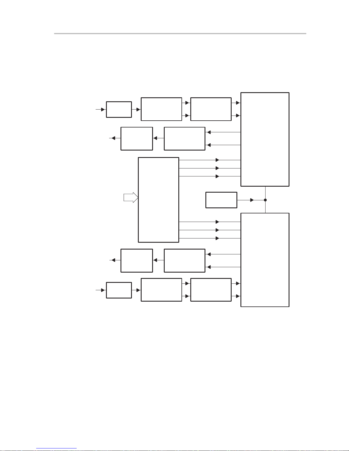
1.2 Block Diagram of AD50-EVM
Figure 1–1 shows the block diagram of the AD50-EVM evaluation
board.
Figure 1–1.AD50-EVM Block Diagram
Block Diagram of AD50-EVM
Audio In
Audio Out
Audio Out
Preamp
DSP Bus
Low Pass
Filter
Programmable
Low Pass
Filter
Level Shift and
Differential
Conversion
Single Ended
Conversion
Logic
Single Ended
Conversion
Antialiasing
Filter
TLC320AD50C
AIC
Serial Interface
Powerdown
FC
Oscillator
FC
Powerdown
Serial Interface
AIC
TLC320AD50C
Audio In
Preamp
The input signal is first buffered and optionally amplified by the preamp stage
before being level-shifted and converted to a differential pair of signals. The
external antialiasing filter is a simple continuous time filter to remove RF noise.
The output from the codec is converted to a single ended signal and is filtered
to remove high frequency noise.
A negative power supply is generated on the AD50-EVM to allow for dc
coupled input and output signals. The clock signal for the codec can be generated by an oscillator on the board or from an external clock. The sampling frequency is set using the programmable clock divider within the AD50. The
AD50 FC, RESET, and POWERDOWN signals can be controlled via a software programmable register.
Level Shift and
Differential
Conversion
Antialiasing
Filter
Introduction
1-3
Page 14

Special Considerations When Using Sigma-Delta Converters
1.3 Special Considerations When Using Sigma-Delta Converters
Sigma-delta analog-to-digital converters typically consist of an analog modulator (fourth order in the case of the AD50) followed by a digital filter section.
The modulator contains a 1-bit ADC (a comparator) which produces a 1-bit
wide data stream, which is applied to the input of the digital filter. It is also applied to the input of a 1-bit DAC, the output of which is fed back to the input of
the modulator. The 1-bit ADC is clocked much faster than the desired output
sampling frequency (F
tization noise generated is uniformly spread over a wide range of frequencies.
A noise-shaping filter within the analog modulator reduces the noise in the
pass-band, increasing it elsewhere. A low-pass digital filter then removes the
unwanted high frequency quantization noise and the signal is resampled at the
desired output frequency.
The sigma-delta DAC in the AD50 consists of a digital interpolating filter operating at 256 × F
S
digital filter removes most of the image frequencies, that would otherwise be
present at the output of a conventional DAC. This avoids the need for a high-order analog low-pass reconstruction filter. Separate sin(x)/x compensation is
not needed, as this is inherent in the DAC architecture.
), (64 × FS for the AD50) and the large amount of quan-
S
followed by a 1-bit DAC and a second-order modulator. The
1.3.1 Advantages
Sigma-delta converters have several advantages and a few disadvantages
relative to other types of ADC which are summarized below.
-
Sigma-delta conversion is inherently linear because there is no reference
resistor chain as in flash or successive approximation converters. This results in extremely low distortion.
-
Inherent monotonicity
-
No missing codes
-
Antialias filtering is inherent within sigma-delta converters. This greatly
simplifies their application, because only a simple external RC filter is required at the input of the ADC to achieve the necessary alias rejection.
-
The digital filters which form an integral part of the ADC and DAC are usually of the finite impulse response type, which gives a linear phase characteristic with high stability.
-
The cutoff frequency of the digital filters automatically tracks the sampling
rate.
-
DAC anti-image filtering is greatly simplified because an internal digital filter attenuates image frequencies. A simple analog filter is sufficient to remove HF noise.
-
No need for sin(x)/x compensation.
-
The sigma-delta architecture is compatible with dense, low-cost, digital IC
processes.
1-4
Page 15

1.3.2 Disadvantages
Special Considerations When Using Sigma-Delta Converters
-
The digital filters in sigma-delta converters introduce into the conversion
process a time delay that makes them unsuitable for some control applications. The AD50 ADC has a delay of 17 samples and the DAC has an 18
sample delay.
-
It is not practical to multiplex several inputs to a single sigma-delta ADC
except at very low rates, because each channel would be corrupted by the
earlier samples from other channels still propagating through the digital
filter. Although the AD50 has an input multiplexer , this is only for selecting
one or another input, not for interleaving two input channels onto one data
stream.
-
Audio band converters are optimized for ac signals and a small dc offset
may be present.
-
Spurious low level tones can sometimes occur at very low input signal
levels, especially if clock signals at Fs/2 are allowed to couple into the
reference voltage pins. Such tones can be identified because their
frequency is affected by small changes in dc offset.
Introduction
1-5
Page 16

1-6
Page 17

Chapter 2
AD50-EVM Design and Construction
This chapter discusses the printed-circuit board design considerations for the
AD50-EVM.
T opic Page
2.1 PCB Construction 2-2. . . . . . . . . . . . . . . . . . . . . . . . . . . . . . . . . . . . . . . . . . . . .
2.2 Power Supply 2-3. . . . . . . . . . . . . . . . . . . . . . . . . . . . . . . . . . . . . . . . . . . . . . . . .
2.3 System Clock 2-3. . . . . . . . . . . . . . . . . . . . . . . . . . . . . . . . . . . . . . . . . . . . . . . . .
2.4 Reset 2-4. . . . . . . . . . . . . . . . . . . . . . . . . . . . . . . . . . . . . . . . . . . . . . . . . . . . . . . .
2.5 Serial Port Interfacing 2-5. . . . . . . . . . . . . . . . . . . . . . . . . . . . . . . . . . . . . . . . .
2.6 Analog Input 2-6. . . . . . . . . . . . . . . . . . . . . . . . . . . . . . . . . . . . . . . . . . . . . . . . . .
2.7 Analog Output 2-10. . . . . . . . . . . . . . . . . . . . . . . . . . . . . . . . . . . . . . . . . . . . . . .
AD50-EVM Design and Construction
2-1
Page 18

PCB Construction
2.1 PCB Construction
The AD50-EVM printed-circuit board is constructed of 4 layers, with ground
and power planes sandwiched between the top and bottom signal-carrying
layers. This minimizes the coupling of RF noise into the system by providing
very low impedance to power and ground, and by shielding signal tracks. The
AD50 is available in two surface-mount packages, the DW and PT . The PT has
a smaller footprint size and is much thinner (only 1.6 mm high). It has 48 pins
at a pitch of 0.5 mm, making it very suitable for PCMCIA and other miniature
applications. However it is difficult to hand solder , and for prototype evaluation
the use of the DW package is recommended. This package has 28 pins at a
pitch of 1.27 mm (0.05 inch) and so is much easier to handle. Surface-mounted
components were used except for the connectors, which through-hole connectors offering robustness.
The printed-circuit board is the same size as the DSK+ board. The AD50-EVM
and the DSK+ can be stacked one above the other using inter-board links. Either board can be on top, but placing the AD50-EVM on top gives better access
to the EVM test points.
A separate connector has been provided for interfacing to systems other than
the DSK+. This brings out the SCLK, FS
Each signal is interleaved with a ground conductor in the ribbon cable, allowing
a longer cable length without crosstalk. Nevertheless, this cable should be as
short as reasonably possible, since ringing in the unterminated cable may become excessive for lengths greater than 3 feet. T o minimize RF emissions, the
cable should be shielded, with the shield connected to the ground plane at the
ground point provided adjacent to pins 1 and 2 of the connector. This connector
must not be used simultaneously with the connections around the edge of the
AD50-EVM board that are specifically intended for the DSK+.
, DIN, DOUT, and RESET signals.
2-2
For the best signal-to-noise ratio, it is often recommended that the
ground plane be split into separate analog and digital sections, joined
together in only one place with the split passing under the AD50 package between its analog and digital ground pins. The split prevents digital noise currents from inducing noise voltages in the analog ground of
the device. The DSK+ has ground and power pins along both edges of
the board, making the use of split ground planes ineffective. Instead
short breaks were inserted on the ground plane to separate the analog
and digital grounds and reduce the common impedance
Page 19

2.2 Power Supply
2.3 System Clock
Power Supply
The AD50-EVM board requires only +5 Vdc; a –5-Vdc supply for some of the
op-amps is generated on the board using a CMOS 7660 charge pump phaselocked to the frame sync output of the AD50. Phase-locking minimizes the risk
of audible beats between the sampling clock and the 7660 clock. The OSC pin
of the 7660 is coupled to the master FSD
with a 22 pF capacitor. This method
allows the 7660 oscillator to free-run when there is no frame sync, ensuring
that the negative power is always maintained, even when the AD50 is held in
reset. The 7660 divides the signal on the OSC pin by 2 internally , ensuring that
the charge pump operates at a 50% duty cycle, even with a grossly asymmetric
input such as that provided by frame sync. Not all negative supply generators
contain a divider. Check before using any other type.
The digital part of the AD50 can be operated at 3.3 V . Users wishing to investigate this should remove R16 and R36 and connect 3.3 V power to L_VD and
R_VD.
When the AD50-EVM is used in standalone mode, in conjunction with a
separate DSP system, a crystal oscillator must be fitted to the socket provided.
A frequency of 10.24 MHz is suggested, as this will allow standard sampling
frequencies such as 10, 16, and 20 kHz to be achieved by programming the
AD50 clock divider and phase-locked loop. Table 2–1 shows the sampling
frequencies that can be selected for a number of master clock frequencies.
Frequencies shown in brackets are above the maximum sampling frequency
specified for the AD50.
In standalone mode the AD50-EVM can be clocked at frequencies up to
22.579 MHz. However, when used in conjunction with the DSK+ the upper
frequency is limited by the maximum clock rate of the TMS320C542 DSP
device. The 10.24 MHz oscillator supplied with the AD50-EVM will drive the
TMS320C542 on the DSK+ at 40.96 MHz, which is only slightly higher than its
maximum operating frequency of 40.00 MHz. However, at room temperature
this should not cause any problems, because the TMS320C542 is tested by
TI at 40.00 MHz over the temperature range 0-70_C. The authors have
successfully operated a DSK+ in conjunction with an AD50-EVM at MCLK
frequencies from 4 MHz to 13 MHz at room temperature, but this may not work
with all DSK+ units. Alternatively, the DSK+ and AD50-EVM clocks can be
separated by removing resistor R80 from the AD50-EVM board and a suitable
oscillator installed on each board. (If this modification is made, 3 and 4 channel
modes will not work correctly because all the AD50s must have an identical
MCLK. Removing R80 prevents the clock from being transmitted between the
boards.)
It is important to ensure that only one oscillator is used in the system (except
as described above), otherwise results will be unpredictable. No damage will
be caused, however, as current limiting resistors are provided on the output
of each oscillator. Electrically it makes no difference whether the oscillator is
fitted to the DSK+, or to the first or second AD50-EVM board.
AD50-EVM Design and Construction
2-3
Page 20

Reset
Table 2–1.Sampling Frequencies for Various MCLK and Register 4 Values
Reg 4, Bit 7 Reg 4, Bits 6–4 8.192 MHz 10.000 MHz 10.240 MHz 11.2896 MHz
0 (default) 8 kHz 9.765 kHz 10 kHz 11.025 kHz
1 (64 kHz) (78.125 kHz) (80 kHz) (88.2 kHz)
2 (32 kHz) (39.063kHz) (40 kHz) (44.1 kHz)
bit 7 = 0
PLL on
bit 7 = 1
PLL off
3 21.333 kHz (26.042 kHz) (26.666 kHz) (29.4 kHz)
4 16 kHz 19.531 kHz 20 kHz 22.05 kHz
5 12.8 kHz 15.625 kHz 16 kHz 17.64 kHz
6 10.666 kHz 13.021 kHz 13.333 kHz 14.7 kHz
7 9.1432 kHz 11.161 kHz 11.429 kHz 12.601 kHz
0 2 kHz 2.441 kHz 2.500 kHz 2.756 kHz
1 16 kHz 19.531 kHz 20 kHz 22.05 kHz
2 8 kHz 9.766 kHz 10 kHz 11.025 kHz
3 5.333 kHz 6.510 kHz 6.666 kHz 7.35 kHz
4 4 kHz 4.883 kHz 5 kHz 5.513 kHz
5 3.2 kHz 3.906 kHz 4 kHz 4.41 kHz
6 2.666 kHz 3.255 kHz 3.333 kHz 3.675 kHz
7 0.798 kHz 2.79 kHz 2.857 kHz 3.15 kHz
2.4 Reset
2-4
In all operating modes the AD50-EVM is reset when the power is switched on.
In DSK+ mode it is also reset when the DSK+ itself is reset. The programmable
logic on the AD50-EVM is configured so that in the reset state all the AD50s
are powered down and in slave mode and that the AC01 on the DSK+ is powered up as normal. This means that even with one or two AD50-EVMs attached
to a DSK+ system, all the DSK+ demonstration software works normally with
the AC01 AIC.
To use one or more AD50s it is necessary to program bits 0-3 of I/O address
0. Bit 0 controls the reset state of the AD50s. Bit 0 = 0 resets all AD50s and
bit 0 = 1 allows them to run. Bits 1, 2, and 3 are encoded to control the number
of AD50s that are powered up (see Table B–1 for details). Note that no provision has been made to operate the AD50s and the AC01 together. This is because their control registers are incompatible and it would be difficult to prevent bus conflicts on the serial interface.
The reset pins are connected to both the SERIAL and CONTROL cable headers for use in standalone mode (see Table A–2 for pinouts).
Page 21

Serial Port Interfacing
2.5 Serial Port Interfacing
The AD50-EVM has been designed to interface to the same synchronous serial port that is used by the AC01 on the DSK+ system. This is achieved by sharing the serial clock, frame sync and data signals, and by powering down the
AC01 when AD50s are in use.
When two AD50-EVMs are connected together the serial interface frame sync
signals need to be configured differently on the primary and secondary boards.
This is achieved using the 22V10 programmable logic device as shown in
Figure 2–1. The logic equations are listed in Appendix B. The serial clock,
serial data in, and serial data out signals are connected to all devices. Only one
device at a time drives these lines.
When two AD50-EVMs are used in standalone mode together with a separate
DSP system, the ribbon cable must be attached to the primary board so that
the master device frame sync signal is transmitted to the external system. The
two AD50-EVM boards have all the necessary signals linked via the four connectors around the periphery.
Figure 2–1.Configuration of Serial Interface on Primary and Secondary AD50-EVMs
FS
22V10
EXT FS
DSK+ Primary
AD50-EVM
FS
AD50
FSD
FS
AD50
FSD
EXT FS
Secondary
AD50-EVM
22V10
FS
AD50
FSD
FS
AD50
FSD
AD50-EVM Design and Construction
2-5
Page 22

Analog Input
2.6 Analog Input
The AD50 can be operated from a single 5 V supply or from a 5 V analog supply
and a 3.3 V digital supply . The AD50-EVM uses 5 V for both analog and digital
supplies to be compatible with the DSK+, and generates an additional –5 V
supply on the board. This negative supply allows the input and output circuitry
to be dc coupled. In an ac coupled system alternative configurations may be
used that do not require a negative supply.
The input circuitry consists of a switchable gain preamp, a single-ended to differential converter with level shifting, and an antialiasing filter.
2.6.1 Preamp Design
This amplifier stage, illustrated in Figure 2–2 allows the use of either a line level
input (approximately 1 Vrms full scale) or a low level input (approximately
100mVrms full scale). With the link labeled
ty gain from dc to 20 kHz. With this link inserted the preamp gain is increased
by 20 dB.
The signal can be ac coupled, by removing the link labeled DC. The use of two
tantalum capacitors back-to-back allows ±10 V dc voltage bias at the input
without damaging the capacitors.
GAIN
removed the preamp has uni-
Figure 2–2.AD50-EVM Input Preamp
DC
2.2 kΩ
IN
4.7 µF
Tant
4.7 µF
Tant
This preamp uses the op amp in the inverting configuration to ensure that the
input common mode range of the op amp cannot be exceeded, since both inputs are always at a voltage close to ground. In the non-inverting configuration
the op amp inputs can approach the supply rails, causing distortion.
2.6.2 Input Stage Design
Gain
22 kΩ
5 V
_
+
–5 V
1 nF
22 kΩ
100 nF
1/2 TLC2272
100 nF
The AD50 analog to digital section uses differential inputs biased at 2.5 V . Maximum code is generated with 3 V
put stage provides the necessary level shifting and single-ended to differential
conversion, prior to the inputs of the AD50.
2-6
PEAK-PEAK
on both differential inputs. The in-
Page 23

Figure 2–3.AD50-EVM Input Stage
Analog Input
10 kΩ
5 V
Input
10 kΩ
5 V
_
+
–5 V
100 nF
10 kΩ
100 nF
1/2 TLC2272
100 nF
10 kΩ
FILT
12 kΩ
10 kΩ
10 kΩ
_
+
10 kΩ
5 V
_
+
100 nF
NEG
1/2 TLC2272
100 nF
POS
1/2 TLC2272
The first op amp inverts the incoming signal, to provide the differential pair
while the second two op amps do the necessary level shifting. The design of
this stage ensures that any noise on FILT appears equally, and in phase, on
both differential inputs. The first op amp needs ±5-V supplies, while the second
two are powered from just 5-V and ground to ensure that the inputs to the AD50
never go below ground.
It is recognized that this device is likely to be used in predominantly digital designs, powered from a single 5 V supply , where the need for a negative supply
could be perceived as a problem. However, since the current drawn from this
negative supply will be small, it is possible to use an inverter chip to provide
a local negative rail for the op amps. The 7660 device requires no external inductors and just 2 external capacitors. Its internal clock can be synchronized
to the codec’s sampling clock, ensuring that any interference generated by the
7660 appears on the codec’s output as a dc offset or at the Nyquist frequency
rather than as noise in the pass-band.
2.6.3 Op Amp Selection
The design of the input stage uses op amps in the inverting configuration. This
has the advantage of keeping both inputs at the reference voltage, preventing
problems with input common mode range.
AD50-EVM Design and Construction
2-7
Page 24

Analog Input
For a full-scale signal the outputs of the op amps that drive the codec inputs
will reach 4 V . Many op amps will not behave well at this output level with a 5-V
supply (in fact the system was tested at 4.75 V to allow for the minimum rated
power supply voltage of the AD50).
Miniature systems often require that analog and digital circuits be in close
proximity to each other. This can lead to problems where radio frequency interference from clock signals or DSP bus lines is demodulated by op amps, leading to an increased DC offset. If the RF is modulated, then that modulation may
appear at the op amp output. CMOS and BiFET op amps can be more resistant
to demodulating RF than bipolar devices. Take particular care to keep digital
signals away from analog ones, and be generous with power supply decoupling and filtering. Power planes help a great deal in reducing system noise.
The authors chose the TI device TLC2272 which is a low noise CMOS dual
op amp designed for single supply operation. It has full rail to rail output swing
and low distortion. However the distortion increases when driving loads of
about 2 kΩ or less.
2.6.4 Antialiasing Filter
Sigma-delta converters have the advantage of providing anti-aliasing filtering
as an integral part of their operation. However this filtering has
multiples of the oversampling frequency . The AD50 is a 64 times oversampling
converter so for a sampling rate of 20 kHz the first
1.28 MHz and will be 20 kHz wide. It is important to ensure that no energy at
this frequency is present across the inputs to the codec. A simple single pole
RC filter is sufficient. If ceramic capacitors are used for this filter they should
be of the COG or NPO dielectric type. Significant distortion can be introduced
by the voltage dependent capacitance of other types of dielectric. Two filter
configurations are possible, as shown in Figure 2–4.
holes
hole
will be centered at
in it, at
Figure 2–4.AD50-EVM Antialiasing Filter Options
TLC320AD50C
+
_
+
_
2-8
4.7 kΩ
INP
1/2 TLC2272
220 pF
4.7 kΩ
INM
1/2 TLC2272
(a)
Figure 2–4a gives good rejection of differential noise signals but common
mode noise is not removed.
Figure 2–4b gives good rejection of common mode noise signals and, if the
capacitors and resistors are well matched, good rejection of differential noise.
+
_
1/2 TLC2272
+
_
1/2 TLC2272
TLC320AD50C
4.7 kΩ
INP
470 pF
4.7 kΩ
INM
470 pF
(b)
Page 25

2.7 Analog Output
Analog Output
Since most noise sources are likely to be coupled equally into both inputs the
filter in Figure 2–4b is usually the best choice (the evaluation board has
footprints to allow for either or both configurations, with the capacitor in
Figure 2–4a not connected).
The AD50 allows higher source impedances at its inputs than many
sigma-delta converters, easing the drive requirements.
The aux inputs also have antialiasing filters connected, allowing the use of
these inputs from external sources without any special filtering requirements.
The antialiasing filter components are placed as close as possible to the inputs
to the AD50 to reduce the possibility of noise pickup between the filter and the
ADC. The use of 0603 footprint surface-mount components makes this
possible.
The AD50 uses a pair of differential voltage outputs. The output stage needs
to convert the differential signals to a single ended output, and to attenuate
noise outside the pass-band. This filter is not a conventional reconstruction filter, since the AD50 has an integral low-pass reconstruction filter. The filter is
a 12-kHz second order low-pass filter designed for use at 20 ksps and will be
less effective at lower sampling rates. Since this filter only removes out of band
noise it will be unnecessary in many applications.
Figure 2–5.AD50-EVM Differential to Single-Ended Output Converter
5.6 k
TLC320AD50C
OUT_P
OUT_M
10 kΩ
10 kΩ
10 kΩ
10 kΩ
5 V
_
+
–5 V
100 nF
1/2 TLC2272
100 nF
2.2 nF
5.6 k
22 kΩ
220 pF
5 V
_
+
–5 V
1/2 TLC2272
100 nF
100 nF
50
Out
AD50-EVM Design and Construction
2-9
Page 26

2-10
Page 27

Chapter 3
Setting Up the AD50-EVM
Setting up the AD50-EVM normally involves coupling it to the synchronous
serial port of a digital signal processing system. Two configurations are
supported. The first is to couple the AD50-EVM to a DSK+ development
system by means of four connectors directly linking the circuit boards together.
The DSK+ consists of a TMS320C542 16-bit fixed point digital signal
processor combined with a 14-bit analog interface circuit and PC printer port
compatible data interface. This allows the downloading and debugging of C
or assembler programs from a DOS or Windows environment. Many example
programs are supplied with the DSK+, which can readily be adapted to
interface to the AD50-EVM. (See Appendix C for detailed information on
adapting example programs.) The second configuration is standalone mode
where a ribbon cable up to 1 m long connects the AD50-EVM to a separate
DSP system. In standalone mode some options such as the number of active
AD50s must be set using jumpers or by control signals from the remote
processor. In DSK+ mode, almost everything is set from software.
Topic Page
3.1 Setting Up for the DSK+ 3-2. . . . . . . . . . . . . . . . . . . . . . . . . . . . . . . . . . . . . . .
3.2 Setting Up for Stand-Alone Mode 3-2. . . . . . . . . . . . . . . . . . . . . . . . . . . . . . .
3.3 Configuring the Serial Interface 3-2. . . . . . . . . . . . . . . . . . . . . . . . . . . . . . . .
3.4 Programming the AD50 Registers 3-3. . . . . . . . . . . . . . . . . . . . . . . . . . . . . .
3.5 Sine-Wave Generator and Loopback Program 3-4. . . . . . . . . . . . . . . . . . .
Setting Up the AD50-EVM
3-1
Page 28

Setting Up the AD50-EVM With the DSK+
3.1 Setting Up the AD50-EVM With the DSK+
The first step is to couple the two circuit boards together using four inter-board
connectors. See Appendix A for full details. The AD50-EVM takes its power
directly from the DSK+. Inputs and outputs are provided on stereo 3.5 mm
jacks. Note that in single channel mode, the active device connects to the ring
contact on the jack. This is conventionally the left channel on stereo headphones. Attaching the AD50-EVM to the DSK+ does not affect the operation
of the AC01 on the DSK+ because the reset default is for both AD50 devices
to be powered down and in slave mode. The master clock source can be the
10.00 MHz oscillator supplied with the DSK+, the 10.24 MHz oscillator provided with the AD50-EVM or any other oscillator module within the capabilities
of the DSK+ (see section 2.3 for details). It does not matter which socket is
used, so long as only one oscillator module is present in the system. Check
that the operation of the SELFTEST and example programs has not been affected by adding the AD50-EVM or the oscillator selection.
Either type in and assemble a program such as the sine-wave generator listed
below, or modify an appropriate example program such as OSCOPE supplied
with the DSK+. Appendix C shows how OSCOPE was modified to work with
the AD50-EVM.
3.2 Setting Up the AD50-EVM in Stand-Alone Mode
In stand-alone mode the AD50-EVM needs to be connected to a system with
a suitable DSP serial interface. This should include a means of controlling the
RESET signal. The connector marked SERIAL has all the necessary signals,
with interleaved grounds. The POWERDOWN and other control signals are
available on the CONTROL connector. In stand-alone mode all the devices are
powered up by default.
A power supply of 5 V at approximately 150 mA needs to be supplied to the
positive (+) and 0 pins of the PSU connector. The negative (–) pin is an output
from the negative voltage converter.
In stand-alone mode an oscillator of up to 22.579 MHz needs to be inserted
in the socket on the AD50-EVM. A 10.24 MHz oscillator is supplied.
Configuration of the registers in the AD50s is software controlled via the serial
interface, as described for the DSK+ mode. However the RESET, POWERDOWN and FC signals need to be set via the CONTROL connector.
3.3 Configuring the Serial Interface
First, the four least significant bits of I/O address 0 must be configured with the
value 2. This selects one AD50 and disables the AC01, holding the AD50 in
reset. Note that the AC01 on the DSK+ is reset by manipulating the XF output
of the C542, whereas the AD50-EVM implements the software reset control
as bit 0 of I/O address 0. This frees the XF bit for other uses, such as driving
3-2
Page 29

an oscilloscope for debugging purposes. Then the ’C542 serial port is initialized to 16-bit mode with external frame sync pulses. The AD50 is then taken
out of reset by writing 3 to I/O address 0. The AD50 starts sending frame sync
pulses and a serial clock signal to the ’C542, which responds by transmitting
data from the serial port. This data consists of a list of alternating primary and
secondary transmissions. The primary transmissions are dummy words with
bit 0 set to 1 to request the interleaved secondary transmissions. Each secondary transmission is a 16-bit word containing commands to initialize the four
control registers of the AD50.
For each secondary transmission, bits 12-8 encode the binary address of the
register to be accessed, bit 13 specifies a read or write access and bits 7–0
contain the data to be written for write operations.
3.4 Programming the AD50 Registers
Register 0 is a dummy register, equivalent in principle to a NOP instruction.
Writing to it does nothing. It is needed so that when several AD50s are cascaded it is possible to modify the control registers of one device without disturbing the others.
Programming the AD50 Registers
Register 1 controls reset and power-down status, input selection, monitor amplifier signal source and gain, digital loop back test mode and 15 or 16 bit DAC
mode. Once 16 bit mode has been selected, it is not possible to request further
secondary communications by setting bit 0 of a serial port data word. However,
the AD50-EVM provides a means for driving the FC pin of the AD50 chip by
writing to bit 0 of I/O address 1. The value written is applied to the FC pin, and
a 1 initiates a hardware secondary communication request. FC is sampled by
the AD50 on the rising edge of frame sync.
Register 2 allows control of the flag bit, reading of the decimator overflow flag,
selection of 15 or 16 bit ADC mode and control of the analog loop back test
mode.
Register 3 is used to select the number of cascaded AD50 devices (up to a
maximum of 1 master and 3 slaves) and to control the time between communications from each device. It is important that register 3 is only programmed
after the sampling frequency has been set. It is convenient to program everything common to all the devices prior to setting register 3. Thereafter, when
secondary communications are requested, each device takes part in turn and
must either be programmed individually or a NOP instruction sent to register
0.
Register 4 controls the analog input and output gains and the sampling
frequency.
It is only necessary to reprogram those registers that have unsuitable default
values. If none of the AD50 registers are programmed, the system will default
to a sampling frequency of 10 kHz for a MCLK frequency of 10.24 MHz. If I/O
address 0 is not programmed as described above, the system will default to
using the AC01 ADC and DAC as normal.
Setting Up the AD50-EVM
3-3
Page 30

Sine-Wave Generator and Loopback Program
3.5 Sine-Wave Generator and Loopback Program
The following code is for a very simple sine-wave generator and loop back program that demonstrates how the DSK+ can be programmed to drive the
AD50-EVM. The sine-wave is generated by means of a lookup table which is
cyclically indexed. This program was used to generate the test waveforms for
the DAC distortion measurements in section 4 below. The sine table delivers
an output waveform at -3dB relative to clipping, to allow direct comparison with
the levels used in the AD50 data book.
This program (AD50SIN.ASM) generates a sine-wave when the assembler
variable
it to the DAC. Filtering code can be inserted if desired. The variable
specifies whether the least significant bit of data written to the DAC is masked
out.
The program should be edited using a text editor (such as MSDOS EDIT) and
assembled as follows:
This generates a binary object file called AD50SIN.OBJ which is loaded into
the DSK+ as follows:
makesine
is set to 1. Otherwise it reads data from the ADC and copies
DSKPLASM AD50SIN
mode16bit
LOADAPP -A AD50SIN.OBJ
.title ”Sine-wave generator for AD50-EVM and C54x DSK+”
.width 80
.length 55
; Adapted from DSK+ example programs by John Walliker and Julian Daley
; June 1997
.mmregs
.setsect ”.text”,0x1800,0 ; these assembler directives specify
.setsect ”.data”,0x0200,1 ; the absolute addresses of different
.setsect ”vectors”,0x0180,0 ; sections of the assembly code
makesine .set 1
mode16bit .set 0
sinestepsize .set 1
sinetablesize .set 20 ; for 1kHz at 20 ksps
; The vectors in this table can be configured for processing external and
; internal software interrupts. The DSKplus debugger uses four interrupt
; vectors. These are RESET, TRAP2, INT2, and HPIINT.
; * DO NOT MODIFY THESE FOUR VECTORS IF YOU PLAN TO USE THE DEBUGGER *
;
; All other vector locations are free to use. When programming always be sure
; the HPIINT bit is unmasked (IMR=200h) to allow the communications kernel and
; host PC interact. INT2 should normally be masked (IMR(bit 2) = 0) so that the
; DSP will not interrupt itself during a HINT. HINT is tied to INT2 externally.
.sect ”vectors”
reset goto #80h ;00; RESET * DO NOT MODIFY IF USING DEBUGGER *
nop
nop
3-4
Page 31

Sine-Wave Generator and Loopback Program
nmi return_enable ;04; non-maskable external interrupt
nop
nop
nop
trap2 goto #88h ;08; trap2 * DO NOT MODIFY IF USING DEBUGGER *
nop
nop
.space 52*16 ;0C-3F: vectors for software interrupts 18-30
int0 return_enable ;40; external interrupt int0
nop
nop
nop
int1 return_enable ;44; external interrupt int1
nop
nop
nop
int2 return_enable ;48; external interrupt int2
nop
nop
nop
tint return_enable ;4C; internal timer interrupt
nop
nop
nop
brint return_enable ;50; BSP receive interrupt
nop
nop
nop
bxint return_enable ;54; BSP transmit interrupt
nop
nop
nop
trint dgoto receive ;58; TDM receive interrupt
nop
nop
txint return_enable ;5C; TDM transmit interrupt
nop
nop
nop
int3 return_enable ;60; external interrupt int3
nop
nop
nop
hpiint goto #0e4h ;64; HPIint * DO NOT MODIFY IF USING DEBUGGER *
nop
nop
.space 24*16 ;68-7F; reserved area
.data
sineindex .word 0 ; index to sine-wave table
sinevalue .word 0 ; workspace for sine-wave generation
Setting Up the AD50-EVM
3-5
Page 32

Sine-Wave Generator and Loopback Program
initwork .word 0 ; workspace for initialization
.text
start: intm = 1 ; disable all interrupts
pmst = #01a0h ; Interrupt pointer maps vectors to address 180h
sp = #0ffah ; stack pointer located in Communications Kernel
imr = #240h ; unmask TDM RINT and HPIINT(host port interface)
OVM = 0 ; OVM = 0 (do not clip overflow)
ASM = #0 ; ASM = 0 (shift=0)
DP = #0
AC01INIT:
; initialize serial port and ad50-evm on-board logic
ar1 = #initwork ; workspace for storing value to be output to ad50-evm
*ar1 = #0010b ; switch on one AD50 and hold it in reset
port(0) = *ar1 ; write the data to i/o port 0
repeat(#23) ; hold reset low for at least 6 mclk cycles
nop ; (4 dsp clock cycles == 1 mclk cycle)
tcr = #10h ; stop timer
imr = #240h ; unmask RXINT and HPIINT
tspc = #0008h ; stop TDM serial port
tdxr = #0h ; send 0 as first xmit word
tspc = #00c8h ; reset and start TDM serial port
*ar1 = #0011b ; bring ad50 out of reset with one channel powered up
port(0) = *ar1
; initialize ad50 registers
a = #0000010010010000b ; register 4
call ad50init ; change fsamp to 20kHz
a = #0000001011000000b ; register 4
call ad50init ; light led
; a = #0000000100000001b ; select 16 bit dac mode
; call ad50init ; this must be the last command
intm = 0 ; enable all interrupts
WAIT idle(1) ; idle waiting for interrupts
nop
goto WAIT
;------------------------------------------------------------------------------; ad50 init routines here
ad50init
ifr = #080h ; clear flag from IFR
tdxr = #01h ; request secondary when AD50 starts
call waitfortdx ; wait for primary to xmit
tdxr = a ; send register value to serial port
ifr = #080h ; clear flag from IFR
call waitfortdx ; wait for secondary to xmit
tdxr = #0h ; send neutral state in case last init
ifr = #080h ; clear flag from IFR
call waitfortdx ; wait for neutral state to xmit
3-6
Page 33

Sine-Wave Generator and Loopback Program
return ; return from subroutine
waitfortdx ; a robust way of waiting for a tdm port
b = mmr(ifr) ; transmission to complete
b &= #10000000b
nop
nop
if(BEQ) goto waitfortdx
return
;-------------------------------------------------------------------------------receive
; save context if necessary
B = mmr(TRCV) ; always read serial port to avoid buffer overflow
; which would stop interrupts from being generated
.if makesine = 0 ; don’t make a sinewave - just echo data from adc to dac
; put code for filtering etc here
.else ; make a sinewave on LEFT channel
AR1 = #sineindex
AR2 = #sinevalue
A = *AR1
A += #sinestepsize
B = A
A -= #sinetablesize
nop ; two nops to allow for pipeline delay
nop
if (ALT) execute(1) ; check whether index points outside table
A = B
*AR1 = A
A += #sinetable20_3dB
*AR2 = prog(A) ; get sinewave value from table in program memory
B = *AR2 ; (could use sine table in rom for this)
.endif
.if mode16bit = 0
B &= #1111111111111110b; mask least significant bit if in 15 bit mode to
.endif ; prevent inadvertent secondary communication requests
mmr(TDXR) = B
; restore context if necessary
return_enable ; return to waiting loop
;-------------------------------------------------------------------------------transmit: ; Transmit and receive interrupts are inherently
; synchronized so there is no point in using both
return_enable
;-------------------------------------------------------------------------------sinetable20_3dB ; -3dB re clipping, 1kHz @ 20 ksps, 20 samples/cycle
.word 0, 7160, 13619, 18745, 22036, 23170, 22036, 18745, 13619, 7160
.word 0, -7160, -13619, -18745, -22036, -23170, -22036, -18745, -13619, -7160
sinetable8_3dB ; -3dB re clipping, 1kHz @ 8 ksps , 8 samples/cycle
.word 0, 16384, 23170, 16384, 0, -16384, -23170, -16384
.end
Setting Up the AD50-EVM
3-7
Page 34

3-8
Page 35

Chapter 4
Results Obtained With AD50 EVM
This chapter describes the results possible with the AD50 EVM. Actual measurements are presented.
Topic Page
4.1 ADC Results 4-2. . . . . . . . . . . . . . . . . . . . . . . . . . . . . . . . . . . . . . . . . . . . . . . . . .
4.2 DAC Results 4-4. . . . . . . . . . . . . . . . . . . . . . . . . . . . . . . . . . . . . . . . . . . . . . . . . .
Results Obtained With AD50 EVM
4-1
Page 36

ADC Results
4.1 ADC Results
T o evaluate the performance of the ADC channel of the AD50-EVM, FFT measurements were performed.
Figure 4–1.AD50-EVM ADC Distortion Measurement at 8 ksps
0
–10
–20
–30
–40
–50
–60
–70
–80
Full Scale – dB
–90
–100
–110
–120
–130
0 0.5 1 1.5 2 2.5 3
Input Signal: 1.1 kHz, –3 dB
FFT: 8ksa/s, 2048 Frequency Bins,
16 Averages
f – Frequency – kHz
3.5 4
Figure 4–1 shows an FFT plot obtained from the ADC of the AD50-EVM. The
input signal was a 1.2-kHz sine wave at -3 dB relative to maximum input. A digital oscillator using a 20 bit DAC was used to produce the test signal. By adding
up the energy in each frequency bin within (a) the signal, (b) the harmonics and
(c) the rest of the noise floor, figures for SNR, SNR and SINAD can be calculated. The figures were 82.9 dB SNR, 79.4 dB SDR and 77.8 dB SINAD. These
figures have not been compensated for noise and distortion components in the
oscillator output.
4-2
Page 37
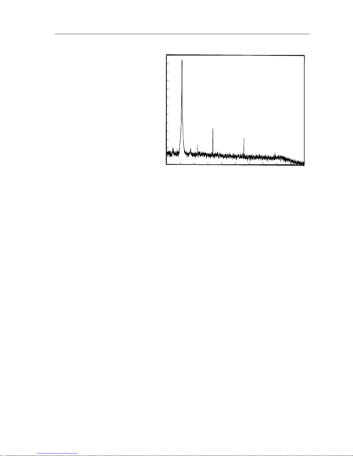
Figure 4–2.AD50-EVM ADC Distortion Measurement at 20 ksps
0
–10
–20
–30
–40
–50
–60
–70
–80
Full Scale – dB
–90
–100
–110
–120
–130
0123 45 6
Figure 4–2 shows an FFT plot obtained from the ADC while sampling at
20 ksps. The performance figures were 82.7 dB SNR, 81.0 dB SDR and
78.7 dB SINAD.
Input Signal: 1.1 kHz, –3 dB
FFT: 20 ksa/s, 2048 Frequency Bins,
16 Averages
f – Frequency – kHz
ADC Results
78910
Results Obtained With AD50 EVM
4-3
Page 38

DAC Results
4.2 DAC Results
The DAC was characterized using a sine-wave table lookup program running
on a TMS320C5x DSK+ coupled to an AD50-EVM.
Figure 4–3.AD50-EVM DAC Distortion Measurement at 8 ksps
0
–10
–20
–30
–40
–50
–60
–70
Full Scale – dB
–80
–90
–100
–110
–120
0123456
AD50 DAC: 8ksa/s Generating a 1 kHz Sine Wave
at–3 dB ref Full Scale
FFT: 40ksa/s, 2048 Frequency Bins, 16 Averages
7111213
8 9 10 14 15 19 2016 17 18
f – Frequency – kHz
Figure 4–3 shows an FFT plot of the output from the AD50-EVM. This was
measured using a T exas Instruments AD55-EVM acquisition system running
at 40 ksps coupled to a DSP development system in a PC.
The signal to noise plus distortion ratio (SINAD) measured in the pass-band
(excluding dc) was 80.5 dB. The SNR was 83.6 dB and the SDR was 83.4 dB.
These measurements have not been adjusted for the noise and distortion of
the acquisition system.
The rise in the noise floor above 4 kHz is due to the digital noise-shaping filter
in the AD50 DAC, which decreases pass-band noise at the expense of increased high frequency noise. This is partially attenuated by the output filter
on the AD50-EVM but continues to rise to a plateau at approximately –100 dB.
This filter is optimized for use at 20 ksps and therefore the out of band noise
is worse than at higher sampling frequencies.
4-4
Page 39

Figure 4–4.AD50-EVM DAC Distortion Measurement at 20 ksps
0
–10
–20
–30
–40
–50
–60
–70
Full Scale – dB
–80
–90
–100
–110
–120
0123456
Similar measurements were made at 20 ksps. The results were 78.6 dB SNR,
84.8 dB SDR and 77.6 dB SINAD. Again this has not been compensated for
the characteristics of the acquisition system.
AD50 DAC: 20 ksa/s Generating a 1 kHz Sine
Wave at –3 dB ref Full Scale
FFT: 40 ksa/s, 2048 Frequency Bins, 16 Averages
78910
f – Frequency – kHz
DAC Results
11 12 13 14 15 16 17 18 19 20
The spike at 10 kHz is caused by breakthrough from the negative supply generator. The larger peaks above 16 kHz are images that have not been completely removed by the reconstruction filters. These are well outside the passband of the DAC.
All the above measurements were made using a well-regulated low noise 5 V
power supply because the power supply shipped with the DSK+ was found to
introduce extra noise.
Results Obtained With AD50 EVM
4-5
Page 40

4-6
Page 41

Appendix A
Installing the AD50-EVM
This chapter discusses the configuration jumper settings for the AD50 EVM,
along with guidelines for connecting it to the DSK+. The parts list, schematics,
gerber plots, and board outline drawings are included.
Topic Page
A.1 Board Outline Drawing With Jumper Locations on the AD50 EVM A-2.
A.2 Connecting the AD50-EVM to the DSK+ A-4. . . . . . . . . . . . . . . . . . . . . . . . .
A.3 Parts List A-4. . . . . . . . . . . . . . . . . . . . . . . . . . . . . . . . . . . . . . . . . . . . . . . . . . . . .
A.4 Circuit Diagrams A-7. . . . . . . . . . . . . . . . . . . . . . . . . . . . . . . . . . . . . . . . . . . . . .
A.5 PCB Diagrams A-??. . . . . . . . . . . . . . . . . . . . . . . . . . . . . . . . . . . . . . . . . . . . . .
Installing the AD50-EVM
A-1
Page 42

Board Outline Drawing With Jumper Locations on the AD50 EVM
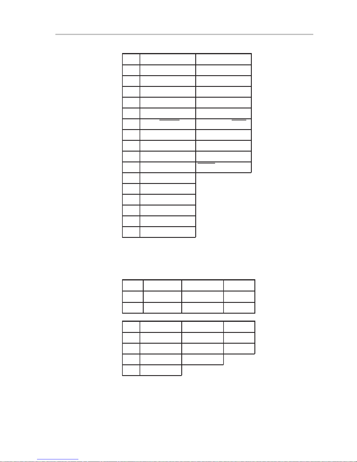
A.1 Board Outline Drawing With Jumper Locations on the AD50 EVM
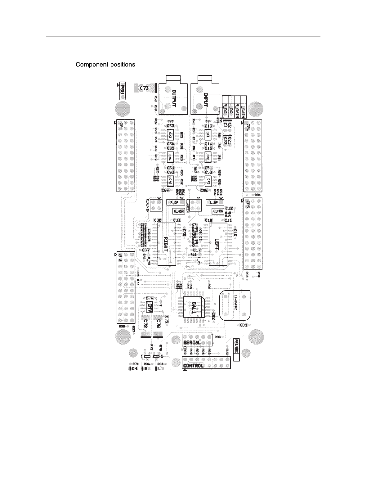
Figure A–1 shows a diagram of the AD50-EVM board showing locations of connectors and jumpers etc.
Figure A–1.Diagram of the AD50-EVM
JP5
L_MON
L_AUXIN
R_MON
R_AUXIN
JP3
L_GAIN
R_GAIN
L_DC
R_DC
INPUT
OUTPUT
PSU
JP4
L_OP
R_OP
JP1
T able A–1.Jumper Positions
OPEN CLOSED DEFAULT
L_DC Left channel ac input coupling Left channel dc input coupling OPEN
R_DC Right channel ac input coupling Right channel dc input coupling OPEN
L_GAIN Left channel 0 dB input gain Left channel 20 dB input gain OPEN
R_GAIN Right channel 0 dB input gain Right channel 20 dB input gain OPEN
PRI/SEC
SERIAL
CONTROL
PRI/SEC Primary board Secondary board OPEN
The connectors marked SERIAL and CONTROL are for use in interfacing the
AD50-EVM to systems other than the DSK+. The pinouts are shown in
Table A–2.
If two AD50-EVMs are used the serial connection should be made to the
primary board.
A-2
Page 43
Board Outline Drawing With Jumper Locations on the AD50 EVM
Table A–2.Control and Serial Connections
Pin Control Serial
1 GROUND GROUND
2 PRI/SEC SERIAL DATA IN
3 GROUND GROUND
4 RIGHT ALTDATA SERIAL DATA OUT
5 GROUND GROUND
6 RIGHT PWRDN LEFT FRAME SYNC
7 RESET GROUND
8 LEFT PWRDN SERIAL CLOCK
9 GROUND GROUND
10 FC RESET
11 GROUND
12 RIGHT FLAG
13 GROUND
14 LEFT FLAG
14 GROUND
16 LEFT ALTDATA
There are 4 sets of connectors that provide direct access to the analog I/O pins
of the AD50. The pinouts for these are shown in Table A–3.
Table A–3.Analog Input/Output Connectors
Label Aux ip Diff-op Mon out
Left L_AUXIN L_OP L_MON
Right R_AUXIN R_OP R_MON
Pin Aux ip Diff-op Mon out
1 AUXP OUTP MONOUT
2 1.25 V GROUND GROUND
3 AUXM OUTM
4 GROUND
There is a set of pins labeled PSU provided for connecting power supplies. The
locally generated –5 V supply can be accessed via this connector.
Installing the AD50-EVM
A-3
Page 44

Connecting the AD50-EVM to the DSK+
A.2 Connecting the AD50-EVM to the DSK+
The two boards are stacked together using plug and socket connectors. Four
pairs of connectors are needed, in JP2, JP3, JP4, and JP5.
The boards can be stacked either way round, although a slightly wider spacing
is needed if the AD50-EVM is on top of the DSK+, due to the height of the audio
jack connectors used on the DSK+. Suitable connectors that will allow the
boards to be stacked either way with a spacing of approximately 13 mm, can
be obtained from the following supplier.
Manufacturer Plug Socket
Samtec
Tel: 1-800-SAMTEC-9 (USA)
+44 1236 739292 (UK)
In order to ensure that the connectors are properly aligned it is suggested that
the plugs and sockets be mated before being soldered to the boards. T o allow
development work with the AD50-EVM it is suggested that the sockets be soldered to the bottom of the AD50-EVM and the pins to the top of the DSK+. This
puts the AD50-EVM on top of the DSK+ and provides good access to the signals on the AD50-EVM
TSW-112-14-T-T SSW-112-21-G-T
If two AD50-EVM boards are being used in conjunction with a DSK+, then a
different socket, with pass through pins, should be used on the middle board.
The Samtec part number is SSQ-112-24-G-T.
A.3 Parts List
Silk Screen
Name
LEFT TLC320AD50CDW OA6 TLC2272ACD
RIGHT TLC320AD50CDW Q1 BC848 SOT23
GAL1 CMOS 22V10 25 ns, PLCC Q2 BC848 SOT23
INV ICL7660 8 pin SO 10–24 MHZ 10.24 MHz 8-pin format TTL or CMOS
ON SM LED 2 mm × 1.25 mm green R1 22K (all resistors 1% 0603)
L SM LED 2 mm × 1.25 mm red R2 (2.2 k) 2K2
R SM LED 2 mm × 1.25 mm red R3 22K
OA1 TLC2272ACD R4 10K
OA2 TLC2272ACD R5 10K
OA3 TLC2272ACD R6 10K
Component
Silk Screen
Name
Component
oscillator module
†
OA4 TLC2272ACD R7 10K
OA5 TLC2272ACD R8 10K
†
British notation used in schematics A–4.
A-4
Page 45

Parts List
Silk Screen
Name
Component
R9 10K R58 (47) 47R
R10 (4.7 k) 4K7
R11 (4.7 k) 4K7
R12 (4.7 k) 4K7
R13 (4.7 k) 4K7
†
†
†
†
Silk Screen
Name
Component
R61 10K
R62 10K
R63 10K
R64 10K
†
R14 56K R65 12K
R15 39K R66 18K
R16 0 Ω link R67 12K
R21 22K R68 47R
R22 (2.2 k)2K2
†
R71 (1.8 k) 1K8
R23 22K R77 10k
R24 10K R78 (4.7 k) 4K7
R25 10K R79 (4.7 k) 4K7
R26 10K R80 (4.7 k) 4K7
R27 10K R81 10k
†
†
†
†
R28 10K R82 10k
R29 10K R83 (470) 470R
R30 (4.7 k) 4K7
R31 (4.7 k) 4K7
R32 (4.7 k) 4K7
R33 (4.7 k) 4K7
†
†
†
†
R84 (470) 470R
R85 10k
R86 10k
R87 10k
†
†
R36 0 Ω link R88 10k
R51 10K R89 10k
R52 10K R90 10k
R53 10K R91 10k
R54 10K R92 10k
R55 12K R93 10k
R56 18K R94 10k
R57 12K R95 10k
R96 10k C30 100 nF X7R 0805
R97 10k C31 100 nF X7R 0805
R98 10k C33 100 nF X7R 0805
R99 10k C34 100 nF X7R 0805
†
British notation used in schematics A–4.
Installing the AD50-EVM
A-5
Page 46

Parts List
Silk Screen
Name
Component
Silk Screen
Name
Component
C1 4.7 µF 10 V size A tantalum C35 100 nF X7R 0805
C2 4.7 µF 10 V size A tantalum C36 100 nF X7R 0805
C3 470 pF COG/NPO 0603 C37 100 nF X7R 0805
C4 470 pF COG/NPO 0603 C51 2.2 nF COG/NPO 0805
C5 470 pF COG/NPO 0603 C52 220 pF COG/NPO 0603
C6 470 pF COG/NPO 0603 C53 100 nF X7R 0805
C7 470 pF COG/NPO 0603 C54 100 nF X7R 0805
C8 470 pF COG/NPO 0603 C61 2.2 nF COG/NPO 0805
C9 470 pF COG/NPO 0603 C62 220 pF COG/NPO 0603
C10 100 nF X7R 0805 C63 100 nF X7R 0805
C1 1 100 nF X7R 0805 C64 100 nF X7R 0805
C12 100 nF X7R 0805 C71 22 pF COG/NPO 0603
C13 100 nF X7R 0805 C72 100 µF 10 V size D tantalum
C14 100 nF X7R 0805 C73 100 µF 10 V size D tantalum
C15 100 nF X7R 0805 C74 100 nF X7R 0805
C16 100 nF X7R 0805 C75 100 nF X7R 0805
C17 100 nF X7R 0805 C76 100 µF 10V size D tantalum
C21 4.7 µF 10 V size A tantalum C81 100 nF X7R 0805
C22 4.7 µF 10 V size A tantalum C82 100 nF X7R 0805
C23 470 pF COG/NPO 0603 INPUT Marushin MJ156L 3.5 mm stereo pcb jack
socket
C24 470 pF COG/NPO 0603 OUTPUT Marushin MJ156L 3.5 mm stereo pcb jack
socket
C25 470 pF COG/NPO 0603 PRI/SEC Right angle header
C26 470 pF COG/NPO 0603 L_DC Right angle header
C27 470 pF COG/NPO 0603 L_GAIN Right angle header
C28 470 pF COG/NPO 0603 R_DC Right angle header
C29 470 pF COG/NPO 0603 R_GAIN Right angle header
A-6
Page 47

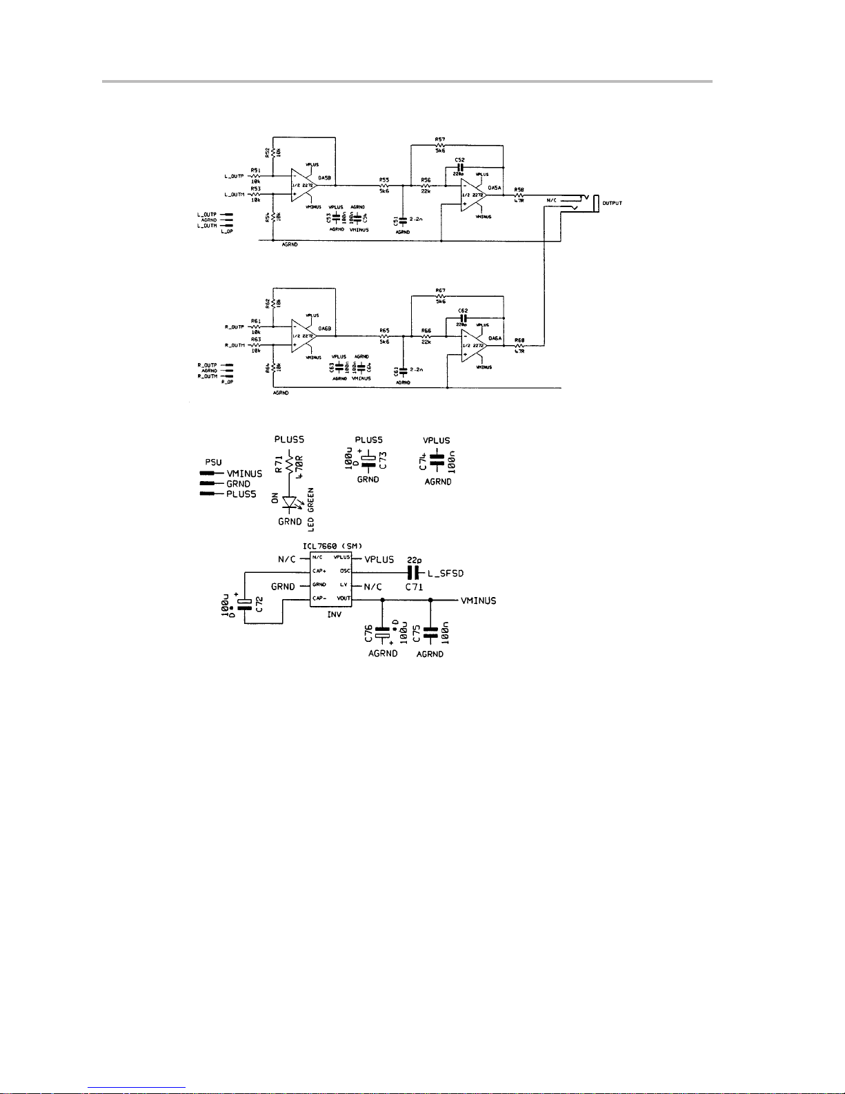
A.4 Circuit Diagrams
Circuit Diagrams
Installing the AD50-EVM
A-7
Page 48
A-8
Page 49

Installing the AD50-EVM
A-9
Page 50

A-10
Page 51

A.5 PCB Diagrams
Top Side Silkscreen
PCB Diagrams
Installing the AD50-EVM
A-11
Page 52

Top Side Tracks
1 – Top Side Tracks
A-12
Page 53

Bottom Side Tracks
Installing the AD50-EVM
A-13
Page 54

Ground plane
A-14
Page 55

Power plane
Installing the AD50-EVM
A-15
Page 56
A-16
Page 57

Appendix B
Programmable Logic
The 22V10 programmable logic device incorporates all the logic needed by the
AD50-EVM when used in stand-alone mode or in conjunction with the DSK+.
Note that in many applications little or no logic is required for interfacing the
AD50 to a DSP system.
When used in stand-alone mode, most of the 22V10 outputs are high impedance to allow an external device complete freedom of control. This is controlled by the state of the DSK_PRESENT signal, which is pulled low when the
AD50-EVM is connected to a DSK+. Otherwise a pull-up resistor makes it default to stand-alone mode.
One or two AD50-EVM boards can provide 1, 2, 3, or 4 simultaneously
sampled channels. When two boards are coupled together the primary/secondary jumper controls the daisy-chaining of serial frame sync pulses and controls the way that data from the DSK+ is interpreted.
Designers familiar with the AC01 should note that the power-down behavior
of the AD50 serial interface is different. The AC01 clock and frame sync outputs are always high impedance in power-down mode. The AD50 clock and
frame sync outputs are driven high in power-down master mode, but are high
impedance in power-down slave mode.
Topic Page
B.1 DSK+ Mode B-2. . . . . . . . . . . . . . . . . . . . . . . . . . . . . . . . . . . . . . . . . . . . . . . . . . .
B.2 Stand-Alone Mode B-2. . . . . . . . . . . . . . . . . . . . . . . . . . . . . . . . . . . . . . . . . . . .
B.3 Logic Compiler Listing B-2. . . . . . . . . . . . . . . . . . . . . . . . . . . . . . . . . . . . . . . .
Programmable Logic
B-1
Page 58

DSK+ Mode
B.1 DSK+ Mode
Address bits 0, 14, and 15 are decoded in conjunction with the I/O space select
and the write enable from the C542 on the DSK+. Signals on the data bus are
latched on the rising edge of the
iostrobe
signal if a valid write address has
been decoded. Bits 14 and 15 are decoded so as to leave 48 k words of contiguous I/O address space free for other hardware that the user might wish to interface to the system. Bit 0 selects one of two control registers implemented
with D latches within the 22V10 device. The first register is used to control the
device reset and
powerdown
inputs for both codecs on each board and to control the powerdown signal to the TLC320AC01 codec on the DSK+ board. The
second register just controls the FC signal. This is to simplify programming of
interleaved secondary communications when the DAC is in 16 bit mode. When
two AD50-EVM boards are used a jumper must be fitted to the primary/secondary header of one of the boards. The board with the jumper becomes the
secondary one and has channels 3 and 4.
The 22V10 must have a propagation delay of 25 ns or less, assuming that one
or more I/O wait states are programmed in the TMS320C542. Zero wait state
operation would have negligible benefit and would need a much faster and
more costly device.
The AD50s are reset either when the DSK+ is reset or when a 0 is programmed
into bit 0 of address 0. Reset must be held low for at least 6 master clock cycles.
The default configuration at reset is for all the AD50s to be powered down and
for the AC01 on the DSK+ to be operating normally . This means that DSK+ will
continue to operate normally until the 22V10 is programmed for AD50 operation.
B.2 Stand-Alone Mode
In stand-alone mode all the logic except that used to link the serial interface
is 3-stated. This allows maximum flexibility to control the AD50s via the
CONTROL and SERIAL cable headers.
Table B–1. AD50-EVM Registers
I/O
Address
0
Bits 15–4 Bit 3 Bit 2 Bit 1 Bit 0 Function
X X X X 0 Hold AD50 in reset
X X X X 1 Release AD50 from reset
X 0 0 0 X AC01 on DSK+ active
X 0 0 1 X 1 AD50 active
1
B-2
X 0 1 0 X 2 AD50s active
X 0 1 1 X 3 AD50s active
X 1 0 0 0 4 AD50s active
X X X X 0 FC pin low
X X X X 1 FC pin high
Page 59

Logic Compiler Listing
B.3 Logic Compiler Listing
TITLE AD50 programmable address decoder & control port
AUTHOR John Walliker and Julian Daley
COMPANY For Texas Instruments
DATE 14 March 1997, 6 April 1997
OPTIONS
EXPAND = ON
INVERSION = OFF ; to ensure correct power–up reset state
MINIMIZATION = ON
CHIP AD50LOGIC EP22V10FN
;PIN 1 NC0
PIN 2 iostrb ; rising edge of DSK+ iostrobe clocks the D latches
PIN 3 DSK_reset ; global reset from DSK+
PIN 4 d0
PIN 5 d1 ; data bus
PIN 6 d2
PIN 7 d3
;PIN 8 NC1
PIN 9 a15
PIN 10 a14 ; address bus
PIN 11 a0
PIN 12 rw ; read/write control signal
PIN 13 primary ; pulled low with jumper when secondary board
;PIN 14 GRND
;PIN 15 NC2
PIN 16 DSK_present ; pulled low when DSK+ is connected
PIN 17 sec_sfs ; secondary serial frame sync
PIN 18 dsk_sfs ; serial frame sync to DSK+
PIN 19 fc ; control signal for initiating secondary comms
PIN 20 AC01_pwrdn ; power down AC01 on DSK+
PIN 21 L_ms ; left master/slave select
;PIN 22 NC3
PIN 23 L_pwrdn ; left power down
PIN 24 R_pwrdn ; right power down
PIN 25 AD50_rst ; reset all AD50s
PIN 26 L_sfs ; left serial frame sync
PIN 27 R_sfsD ; right serial frame sync delayed
;PIN 28 VCC
STRING select0 ’(/a0 * /a14 * /a15 * /rw)’ ; address decode
STRING select1 ’( a0 * /a14 * /a15 * /rw)’
EQUATIONS
AD50_rst := select0 * d0 ; primary and secondary boards are driven
+ /select0 * AD50_rst
AD50_rst.clkf = iostrb
AD50_rst.rstf = /DSK_reset
AD50_rst.trst = /DSK_present ; 3-state if in standalone mode
fc := select1 * d0
+ /select1 * fc
fc.clkf = iostrb
fc.rstf = /DSK_reset
Programmable Logic
B-3
Page 60

Logic Compiler Listing
fc.trst = /DSK_present
/AC01_pwrdn := select0 * (d3 + d2 + d1) ; NB The logic assembler MUST NOT in-
vert
+ /select0 * /AC01_pwrdn ; equations, otherwise power–up reset
; state will be incorrect!
AC01_pwrdn.clkf = iostrb
AC01_pwrdn.rstf = /DSK_reset
L_pwrdn := select0 * /d3 * /d2 * d1 * primary
+ select0 * /d3 * d2 * /d1 * primary
+ select0 * /d3 * d2 * d1
+ select0 * d3 * /d2 * /d1
+ /select0 * L_pwrdn
L_pwrdn.clkf = iostrb
L_pwrdn.rstf = /DSK_reset
L_pwrdn.trst = /DSK_present
L_ms = primary * L_pwrdn * /DSK_present
+ primary * DSK_present
R_pwrdn := select0 * /d3 * d2 * /d1 * primary
+ select0 * /d3 * d2 * d1 * primary
+ select0 * d3 * /d2 * /d1
+ /select0 * R_pwrdn
R_pwrdn.clkf = iostrb
R_pwrdn.rstf = /DSK_reset
R_pwrdn.trst = /DSK_present
DSK_sfs = L_sfs
DSK_sfs.trst = primary * /AC01_pwrdn
L_sfs = sec_sfs
L_sfs.trst = /primary
sec_sfs = R_sfsd
sec_sfs.trst = primary
B-4
Page 61

Appendix C
Converting DSK+ Software for the AD50-EVM
The AD50-EVM has been designed to make conversion of DSK+ programs
originally written for the AC01 analog interface circuit as easy as possible. The
serial port used by the AC01 is shared with two or four AD50s fitted to one or
two AD50-EVM boards, but logic ensures that only one type of AIC is used at
a time.
For single channel operation the only essential changes to existing code relate
to initialization. First, one AD50 must be switched on and held in reset for at
least 6 master clock cycles. While it is held in reset the DSP serial port is initialized. The AD50 is then released from reset and the registers of the AD50 are
programmed with the required clock division ratio, analog gains etc.
It is not essential to change the main program code for single channel operation, as the AD50 uses the same serial port as the AC01. However, the AC01
is a 14-bit device whereas the AD50 supports 15- or 16-bit operations. For best
performance, therefore, masking operations that strip the two least significant
bits from data sent to or from the AC01 should be modified to remove only bit
0 or removed completely, depending on whether 15- or 16-bit mode is to be
used.
The following code shows how the oscilloscope program (OSCOPE) supplied
with the DSK+ was modified to use one AD50 device instead of the AC01. OSCOPE provides an oscilloscope style display of the input waveform on the PC
screen. This program is split up into several modules, with all the ADC initialization code in OSC_AC01.ASM.
The C54x algebraic assembly language is used. Code that has been added
italics
is shown in bold, while code that has been deleted is shown in
changes were made to the C code running on the PC for transferring and displaying the acquired data, so this code is not listed below.
. No
Converting DSK+ Software for the AD50-EVM
C-1
Page 62

; ***************************************************************************
; File: OSC_MAIN.ASM –> DSKplus Oscilloscope ASM file for the ’C54x DSKplus
; Adapted to operate with AD50–EVM by John Walliker and Julian Daley
; ***************************************************************************
.width 80
.length 55
.title ”DSKplus Oscilloscope program”
.mmregs
.setsect ”.text”, 0x500
.setsect ”vectors”,0x180
;======================================================================
;
; VECTORS
;
;======================================================================
.sect ”vectors”
.copy ”osc_vecs.asm”
.text
start:
call AC01INIT
pmst = #01a0h ; set up iptr
sp = #0ffah ; init stack pointer.
ar2 = #1200h ; pointer to receive buffer.
*ar2+ = data(#0bh) ; store to rcv buffer
imr = #40h
intm = 0 ; ready to rcv int’s
wait nop
goto wait
; –––––––––––––––– Receive Interrupt Routine ––––––––––––––––––
RINT:
b = trcv ; load acc b with input
b = #0FFFEh & b ; only strip out lsb for AD50
*ar2+ = data(#0bh) ; store to rcv buffer
tdxr = b ; transmit the data.
TC = (@ar2 == #01300h)
if (TC) goto restrt ; stop if rcv buffer is at 1300h
return_enable
restrt
ar2 = #1200h ; set intm bit ...no int’s
hpic = #0ah ; flag host task completed
return_enable
; ––––––––––––––––––––––– end ISR ––––––––––––––––––––––––––––
.copy ”osc_ac01.asm”
.end
;***************************************************************************
; File: Osc_AC01.ASM –> AC01 Init Routine for the Oscillocope application
; Adapted to operate with AD50–EVM by John Walliker and Julian Daley
;***************************************************************************
.width 80
.length 55
C-2
Page 63

.title ”AC01 Initialization Program”
.mmregs
***************************************************************************
* Certain AC01 registers can be initialized using a conditional assembly
* constant. By setting the constant REGISTER to the appropriate value, the
* assembler will either include initialization for certain registers or
* ignore register initialization.
*
* The constant REGISTER should be set to include the following AC01 register:
*
* REGISTER (binary) =
*
* 0000 0000 0000 0001 –> initialize Register 1 (A Register)
* 0000 0000 0000 0010 –> initialize Register 2 (B Register)
* 0000 0000 0000 0100 –> initialize Register 3 (A’ Register)
* 0000 0000 0000 1000 –> initialize Register 4 (Amplifier Gain–Select)
* 0000 0000 0001 0000 –> initialize Register 5 (Analog Configuration)
* 0000 0000 0010 0000 –> initialize Register 6 (Digital Configuration)
* 0000 0000 0100 0000 –> initialize Register 7 (Frame–Sync Delay)
* 0000 0000 1000 0000 –> initialize Register 8 (Fram–Sync number)
*
* For AD50–EVM
* 0000 0000 0000 0001 –> initialize Register 1
* 0000 0000 0000 0010 –> initialize Register 2
* 0000 0000 0000 0100 –> initialize Register 3
* 0000 0000 0000 1000 –> initialize Register 4
*
*
Any combination of registers can be initialized by adding the binary
* number to the REGISTER constant. For example to initialize Registers 4
* and 5, REGISTER = 18h. Upon assembly, only code for register 4 & 5
* initialization is included in the AC01INIT module. When called the
* module will load the REG4 and REG5 values into internal AC01 registers.
*
;;
REGISTER .set 09h ; Powerup default values:
;;
REG1 .set 120h ;*A=32 112h
;;
REG2 .set 212h ; 212h
;;
REG3 .set 300h ; 300h
;;
REG4 .set 409h ;* 405h
;;
REG5 .set 501h ; 501h
;;
REG6 .set 600h ; 600h
;;
REG7 .set 700h ; 700h
;;
REG8 .set 801h ; 801h
;For AD50–EVM:
REGISTER .set 1000b ; just program reg 4
REG1 .set 0000000100000000b ; default
REG2 .set 0000001000010000b ; select 16–bit ADC mode
REG3 .set 0000001100000000b ; default (no slaves)
REG4 .set 0000010010010000b ; 20ksa/s with 10.24MHz MCLK
; Note that once 16–bit DAC mode has been selected in reg 1, bit 0, other
; registers can only be configured by using FC to request secondary comms. On the
Converting DSK+ Software for the AD50-EVM
C-3
Page 64

; AD50–EVM this can be achieved by writing 1 to i/o port 1, bit 0 before a primary
; communication and clearing port 1 afterwards.
; Once slave devices have been specified using reg 3, then a separate secondary
; communication (interleaved with normal communications) takes place for each
; device in turn.
AC01INIT:
ar2 = #1302h ; workspace for storing value to be output to AD50–EVM
*ar2 = #0010b ; switch on one AD50 and hold it in reset
port(0) = *ar2 ; write the data to i/o port 0
repeat(#50) ; hold reset low for at least 6 mclk cycles
nop ; ( 4 DSP clock cycles == 1 MCLK cycle )
;;
xf = 0 ; reset ac01
intm = 1 ; disable all int service routines
tcr = #10h ; stop timer
imr = #280h ; wakeup from idle when TDM Xmt int
tspc = #0008h ; stop TDM serial port
tdxr = #0h ; send 0 as first xmit word
tspc = #00c8h ; reset and start TDM serial port
;;
xf = 1 ; release ac01 from reset
*ar2 = #0011b ; bring ad50 out of reset with 1 channel selected
port(0) = *ar2
; ––––––––––––––– Register init’s ––––––––––––––––––––––––––––––
.eval REGISTER & 1h, SELECT ; if REG1 then include this source
.if SELECT = 1h ;
a = #REG1 ; load Acc A with REG1 value
call REQ2 ; Call REQ2 subroutine
.endif
.eval REGISTER & 2h, SELECT ; if REG2 then include this source
.if SELECT = 2h
a = #REG2
call REQ2
.endif
.eval REGISTER & 8h, SELECT ; if REG4 then include this source
.if SELECT = 8h
a = #REG4
call REQ2
.endif
; Note that AD50 register 3 must be programmed last!
.eval REGISTER & 4h, SELECT ; if REG3 then include this source
.if SELECT = 4h
a = #REG3
call REQ2
.endif
; Code for registers not used by AD50 deleted
return
REQ2
ifr = #080h ; clear flag from IFR
tdxr = #03h ; request secondary when AC01 starts
call waitfortdx ; wait for primary to xmit
tdxr = a ; send register value to serial port
C-4
Page 65

ifr = #080h ; clear flag from IFR
call waitfortdx ; wait for secondary to xmit
tdxr = #0h ; send neutral state in case last init
ifr = #080h ; clear flag from IFR
call waitfortdx ; wait for neutral state to xmit
return ; return from subroutine
waitfortdx ; a robust way of waiting for a tdm port
b = mmr(ifr) ; transmission to complete
b &= #10000000b
nop
nop
if(BEQ) goto waitfortdx
return
.end
; ***************************************************************************
; File: osc_vecs.ASM –> Vector Table for the ’C54x DSKplus Oscilloscope
;
; ***************************************************************************
.width 80
.length 55
.title ”Vector Table”
.mmregs
reset dgoto start ;00; RESET
IMR = #200h
nmi return_enable ;04; non–maskable external interrupt
nop
nop
nop
trap2 return_enable ;08; trap2
nop
nop
nop
.space 52*16 ;0C–3F: vectors for software interrupts 18–30
int0 return_enable ;40; external interrupt int0
nop
nop
nop
int1 return_enable ;44; external interrupt int1
nop
nop
nop
int2 return_enable ;48; external interrupt int2
nop
nop
nop
tint return_enable ;4C; internal timer interrupt
nop
nop
nop
brint return_enable ;50; BSP receive interrupt
Converting DSK+ Software for the AD50-EVM
C-5
Page 66

nop
nop
nop
bxint return_enable ;54; BSP transmit interrupt
nop
nop
nop
trint goto RINT ;58; TDM receive interrupt
nop
nop
txint return_enable ;5C; TDM transmit interrupt
nop
nop
nop
int3 return_enable ;60; external interrupt int3
nop
nop
nop
hpiint return_enable ;64; HPIint
nop
nop
nop
.space 24*16 ;68–7F; reserved area
C-6
 Loading...