

Page 1

AM335xStarterKitHardwareUsersGuide
1
AM335xStarterKitHardwareUsersGuide
AM335x Starter Kit Hardware User Guide
Introduction
This document provides the design information on the AM335x processor based Starter Kit (TMDSSK3358) to
users.
Description
The AM335x Starter Kit (TMDSSK3358) can be used as an evaluation and development platform for low cost
AM335x based solutions and networking platforms. The embedded emulation logic allows emulation and debug
using standard development tools such as TI’s Code Composer Studio by just using the supplied USB cable. It is not
intended for use in end products. All of the design information is freely available and can be used as the basis for the
development of an AM335x based product.
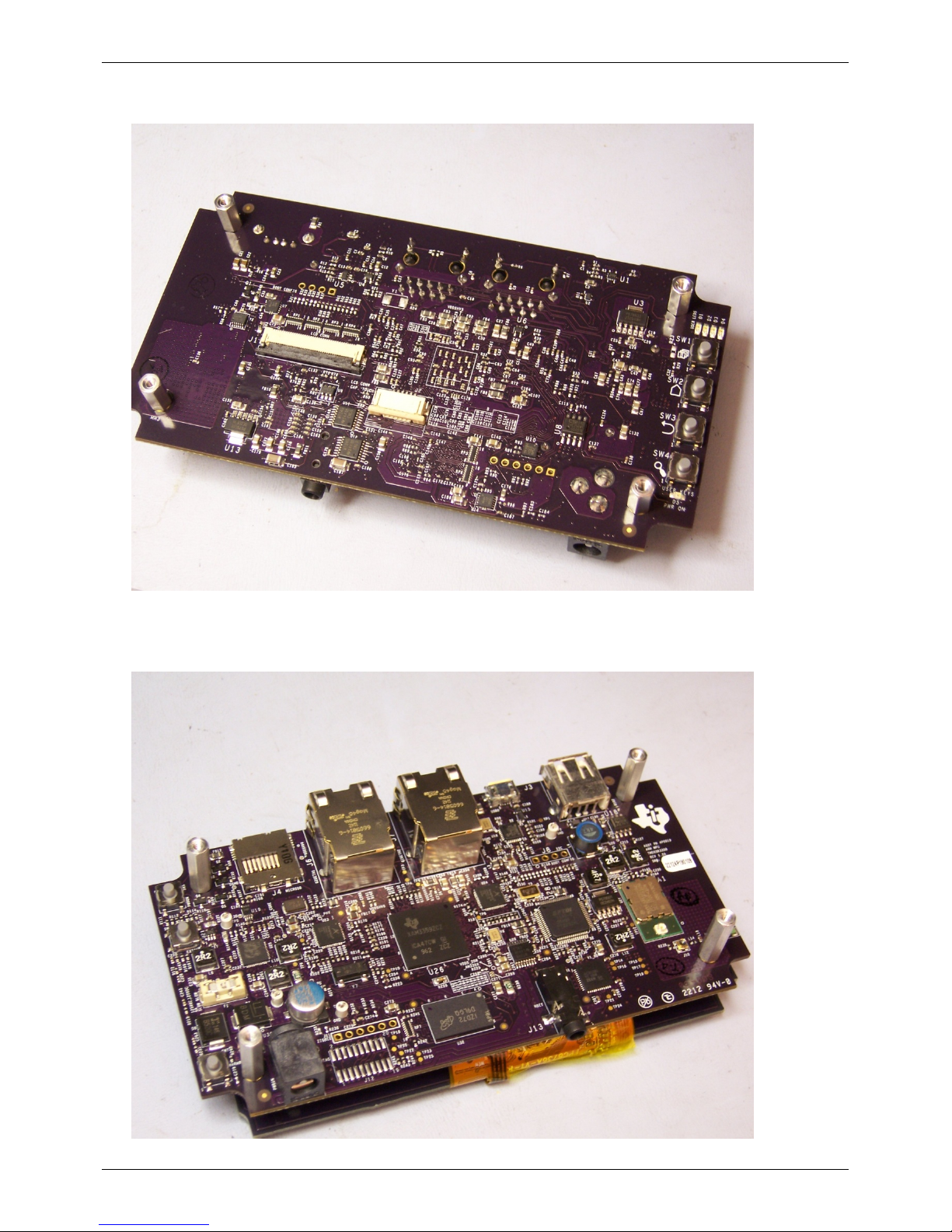
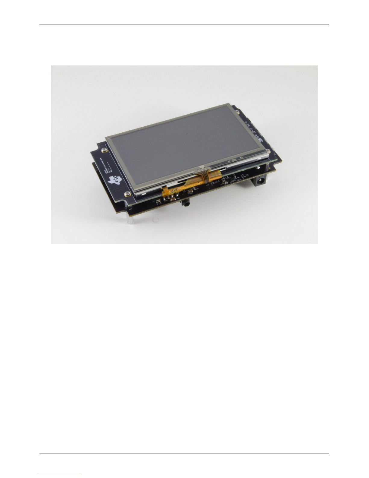
EVM System View
TMDSSK3358 is partitioned into two different boards: the main board (processor, peripherals & the main power
supply) and the LCD Carrier board (LCD and touch screen). The TMDSSK3358 main board and the LCD carrier
board mounted are mounted together using 10mm standoffs. The TMDSSK3358 main board has dimensions of
5.257” x 2.798 “and that of the LCD Carrier board is 4.963” x 2.798 “. The Top and the Bottom side views of the
TMDSSK3358 are shown in the pictures provided below.
Page 2
AM335xStarterKitHardwareUsersGuide
2
Top view
Figure 1: TMDSSK3358 Top view
Bottom view
Page 3
AM335xStarterKitHardwareUsersGuide
3
Figure 2: TMDSSK3358 V1.2A Bottom View
System view
Figure 3: TMDSSK3358 System View
Page 4
AM335xStarterKitHardwareUsersGuide
4
Schematics/Design Files
• HW Documentation
[1]
- Schematics, Design Files, and other related HW Documentation
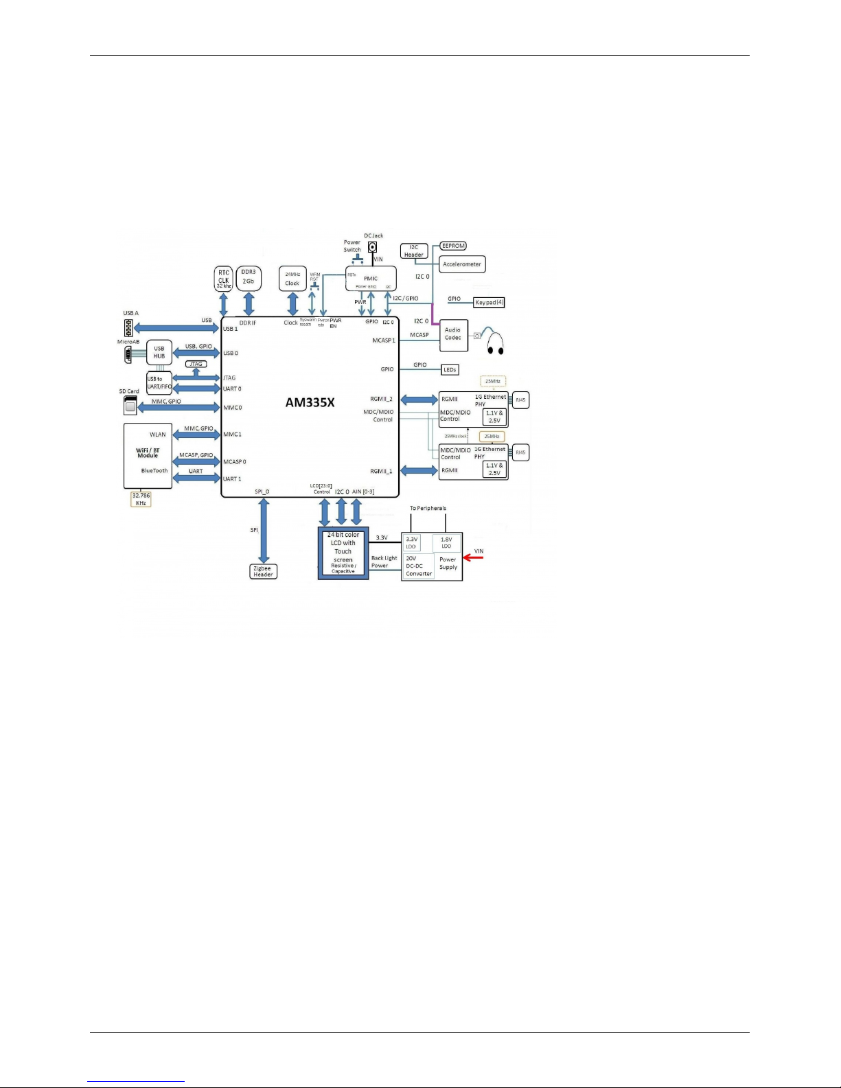
Functional Block Diagram
This section describes about the major functional blocks of the TMDSSK3358. The Functional block diagram of the
TMDSSK3358 design is shown below.
Figure 4: TMDSSK3358 Block Diagram
Processor
The AM3358ZCZ processor is the central processor for TMDSSK3358. All the resources on the board surround the
AM3358 processor to provide development capabilities for hardware and software. See the AM3358 datasheet and
TRM for the details about the processor.
There are system configuration signals, SYSBOOT, that can be set on the EVM to define some startup parameters on
the AM335x processor. See the Configuration/Setup section later for more details.
Page 5

AM335xStarterKitHardwareUsersGuide
5
Clocks
The main clock for the processor is derived from a 24MHz crystal. An on-board oscillator in the AM3358 generates
the base clock and subsequent module clocks as needed within the AM3358 processor. A 32kHz clock for the RTC
on the AM3358 is derived from a 32kHz crystal on board.
Reset Signals
Power On Reset to the AM335x is driven by the PMIC. SYS_ WARMRESETn is a signal running to several
peripherals and AM335x which performs a reset on those peripherals. SYS_WARMRESETn is asserted by a
pushbutton on the main board and is used to force a reset of the AM335x. AM335x can also pull down on the
RESET_INOUTn signal to cause the SYS_ WARMRESETn line to go active. The RTC_PORZ reset signal for the
RTC section is derived using AND Gates.
Power
The power input to TMDSSK3358 is from a 5V Power Supply. This 5V power is provided as power input to the
Power Manager TPS65910A3. The power requirements of the processor are taken care of by the Power Manager IC
TPS65910A3. The Power ON LED "D5" is ON if the PMIC output power VAUX33 is available ( to indicate the
active status of the PMIC). The power sequencing requirements of the AM335X processor (see the AM335x
datasheet) are handled automatically by the TPS65910A3 PMIC.
Note: When powering the TMDSSK3358 EVM, always use the supplied power supply (CUI/V-Infinity Part
Number EMSA050300-P6P-SZ, Model 3A-182WP05) or equivalent model having output voltage of +5VDC
and output current max 3.0 Amps.
Power Management IC
TMDSSK3358 uses the TPS65910A3 power management IC. The I2C0 on AM335x is used to control the
TPS65910A PMIC.
The PWRON input of PMIC is connected to an external push-button. The built-in debouncing time defines a
minimum button press duration that is required for button press detection. Any button press duration which is lower
than this value is ignored, considered an accidental touch.
For AM335x, the following power supplies from the TPS65910A are used.
TPS65910 Power Supply/Other sources AM335x Power Rail Voltage
VAUX2 (300mA) VDDSHV6 (300mA) 3.3V
VMMC (300mA) VDDSHV2,3,4,5 (300 mA), VDDA3P3V_USB0/1 (10 mA) 3.3V
VDD2 SMPS (1500mA) VDD_CORE (1000mA) 1.1V
VDD1 SMPS (1500mA) VDD_MPU (1500mA) 1.2V
No supply needed VDD_RTC 1.1V
VRTC (External LDO) VDDS_RTC (10mA) 1.8V
VIO_SMPS (1000mA) VDDS_DDR (200mA) 1.5V
VIO_SMPS (1000mA) DDR_VREF (10mA) 0.9V
VDAC (150mA) VDDS (100mA) 1.8V
VDIG1 (300mA) VDDSHV1 1.8V
VDIG2 (300mA) VDDS_SRAM_CORE_BG (40mA) 1.8V
VDIG2 (300mA) VDDS_SRAM_MPU_BB (40mA) 1.8V
Page 6
AM335xStarterKitHardwareUsersGuide
6
VDIG2 (300mA) VDDS_PLL_DDR (25mA) 1.8V
VDIG2 (300mA) VDDS_PLL_CORE_LCD (25mA) 1.8V
VDIG2 (300mA) VDDS_PLL_MPU (25mA) 1.8V
VDIG2 (300mA) VDDS_OSC (10mA) 1.8V
VAUX1 (300mA) VDDA1P8V_USB0/1 (50mA) 1.8V
VPLL (50mA) VDDA_ADC 1.8V
VDD3 SMPS (100mA) Not Used -
Table 1: Power supplies to AM335x from TPS65910A3 PMIC
Configuration/Setup
Boot Configuration
Various boot configurations can be set using the pull up / down resistor combinations provided on the SYS_BOOT
pins (LCD_DATA0..15).Boot configuration pins are latched upon de-assertion of PORz pin.
I2C Port Address Assignments
Information on I2C address assignments are provided below.
AM335x STARTER KIT (TMDSSK3358) Function AM335x I2C Port Address
Baseboard ID memory I2C0 0x50
AM355x PMIC Control I2C0 0x2D
AM355x PMIC Smart Reflex Control I2C0 0x12
Accelerometer Control I2C0 0x18
Audio Codec I2C0 0x1B
Capacitive Touch screen I2C0 0x38
Table 2:I2C Bus Addresses
Memories Supported
The TMDSSK3358 design supports on-board memories like DDR3 SDRAM and Board ID EEPROM. It also
supports an SD card socket.
DDR3 SDRAM
DDR3 SDRAM memory design is provided by using a 2 Gb single chip solution (MT41J128M16JT-125) from
Micron. It is internally configured as a16 Meg x 16 x 8 bank memory. A separate Regulator to supply the DDR
reference power to the AM335x and the VTT termination voltage to the termination components is provided in the
design. The VIO_SMPS output from the PMIC is programmed to provide the required 1.5V to the DDR3 SDRAM.
Page 7

AM335xStarterKitHardwareUsersGuide
7
Board Identity Memory
The board contains a serial EEPROM with the board specific data which allows the processor to automatically detect
which board is connected and the version of that board. Other hardware specific data can be stored in this memory as
well. The part number of the memory device used is CAT24C256WI-GT3. See the Configuration/Setup section for
details on the data in this memory.
Name Size
Contents
Header 4 MSB 0xEE3355AA LSB
Board Name 8 Name for board in ASCII “A335X_SK” = AM335x TMDSSK3358Board
Version 4 Hardware version code for board in ASCII “1.2A” = rev. 01.2A
Serial Number 12 Serial number of the board. This is a 12 character string which is: WWYY4P19nnnn where: WW = 2 digit week of the
year of production YY = 2 digit year of production nnnn = incrementing board number
Configuration
Option
32 Codes to show the configuration setup on this board. For the available EVM’s supported, the following codes are used:
ASCII “SKU#00” = default configuration Remaining 26 bytes are reserved
Available 32720 Available space for other non-volatile codes/data
Table 3:I2C Configuration
SD/MMC0
The Micro SD/MMC0 port is provided with a card socket SCHA5B0200. This is a standard Micro SD/MMC Card
type of connector which is of the low profile compact type. It is connected to the MMC0 port of the AM335x
processor. Check the AM335x data sheet and TRM for supported card types/densities.8Gb SD cards are tested with
this design. The Pin assignment is as given below.
Pin No Memory Card PIN No.
uSD#1 DAT2
uSD#2 CD/DAT3
uSD #3 CMD
uSD #4 VCC
uSD #5 CLK
uSD #6 GND
uSD #7 DAT0
uSD #8 DAT1
uSD #9 GND
uSD #10 CD
Table 4: SD/MMC0 Connector Pin Details
Ethernet
TMDSSK3358 has two Giga bit Ethernet transceivers. AR8031-AL1A from Atheros is used as a single port, tri
speed PHY. A single 3.3V is enough to power this PHY and the other voltages required were generated internally.
Reset for both the chips are driven by the SYS_WARMRESETn signal through a SN74LVC1G07 buffer.Both the
PHYs have individual 25MHz, 50ppm crystal as their clock source. The 25MHz Clock out of the EMAC1-PHY port
has been connected to the XTLI of the EMAC2-PHY as an optional clock input.
Page 8

AM335xStarterKitHardwareUsersGuide
8
For both the PHYs, mode selection pins MODE [3:0] are set as “0000” to operate it in 1000 BASE-T, RGMII mode.
The PHY address for the EMAC1-PHY and EMAC2-PHY are 00100 and 00101 respectively.The interrupts from the
both PHYs are connected to both the Non Maskable Interrupt pin and to the processor GPIO pins.
The Wake On LAN interrupts from the both PHYs are connected to the EXT_WAKEUP signal of the processor as
an option.
Pin No Signal Name Description
1 DGND Ground
2 NC No connect
3 ETHER_D3P MDI 3 POSITIVE
4 ETHER_D3N MDI 3 NEGATIVE
5 ETHER_D2P MDI 2 POSITIVE
6 ETHER_D2N MDI 2 NEGATIVE
7 ETHER_D1P MDI 1 POSITIVE
8 ETHER_D1N MDI 1 NEGATIVE
9 ETHER_D0P MDI 0 POSITIVE
10 ETHER_D0N MDI 0 NEGATIVE
D1 PHY_ LED_ACTn PHY ACTIVITY LED signal
D2 GND Ground
D3 GND Ground
D4 PHY_ LED_1000n 1000 Base-T LINK LED signal
Table 5: 10/100 PRU Ethernet1 Pin Details
USB
USB to UART/JTAG
Micro AB USB port is provided as an upstream port of the USB HUB USB2412. This is used for USB to JTAG and
USB to UART conversion applications through the downstream port 1 of the HUB. FT2232L is used for the USB to
UART and JTAG conversion applications. The Downstream port 2 of the Hub is connected to USB port 0 of the
AM335x.
The USB to UART/JTAG converter (FT2232L) has 32 configurable multifunction pins. A 16 bit, serial EEPROM
93LC56B from MicroChip is used to store the configuration data. Some of the pins from ADBUS [7:0] and ACBUS
[7:0] are configured as JTAG and Reset signals. These JTAG pins from the FT2232 IC are connected to the
dedicated processor JTAG pins and as well to the optional JTAG connector.
The Micro AB USB pin out details are provided below.
Page 9

AM335xStarterKitHardwareUsersGuide
9
Pin No Signal Name Description
1 USB_DC USB BUS VOLTAGE
2 USBDM_UP USB DATA MINUS
3 USBDP_UP USB DATA PLUS
4 NC (USB_ID) No connect
5 DGND Ground
Table 6: Micro AB – USB0
USB 1
The USB port1 of the AM335x is connected to the USB type A connector. USB power (5V )is provided to this
connector through a buck-boost converter circuit.
Pin No Signal Name Description
1 VUSB_VBUS1 USB BUS VOLTAGE
2 USB1_CONN_DM USB1 DATA MINUS
3 USB1_CONN_DP USB1 DATA PLUS
4 DGND Ground
Table 7: USB A Type – USB1
Audio Codec
The TLV320AIC3106 is a low-power stereo audio codec with stereo headphone amplifier from TI. CLKOUT1 of
the processor is sourcing the master clock of the codec (24Mhz). The CODEC I2C is capable of supporting both the
standard and fast modes. I2C address of the codec is configured as 0011011. MCASP1 interface of the processor is
connected to the audio interface of the codec. The stereo audio output is terminated in a stereo headphone Jack. The
Pinout assignments for the headset jack are provided below.
Pin No Signal Description
1 AGND_AUD Analog Ground
3 HS_SPKRP Headset stereo LOUT
10 NC No Connect
2 HD_SPKRP Headset stereo ROUT
Table 8: Headset Jack
WLAN
LBEE5ZSTNC-523 Type TN WiFi / BT Module from Murata is used to provide the WLAN and the Bluetooth
connectivity for the TMDSSK3358 design. The WLAN design has IEEE802.11 b, g, n compliance for WLAN and
Version4.0 with Blue tooth Low Energy (BLE) for BT. This module requires an external 32.768 KHz, +/-150ppm
clock. This is sourced by the CLKOUT2 clock out pin of the processor. The required digital interfaces for the
module are connected to the UART1 and McASP0 ports of the processor through voltage level converters.
Note that due to a HW bug in the WiFi Antenna matching network design, customers may observe significant
degradation in throughput (15-20 Mbps - Typical) as well as reduced WiFi Range when using the AM335x Starter
Kit and COM6M module with AM335-EVM, with the onboard WiFi Antenna.
Page 10

AM335xStarterKitHardwareUsersGuide
10
For optimal throughput we recomend using an external Antenna as describe in the link:<ECO for using external
antenna>
[2]
Warning: To minimize risks of potential radiation hazards associated with handling and/or moving the
energized EVM including compliance with the wireless radio grant licensing provisions, always maintain a
minimum distance of 20cm measured between EVM user(s) and the EVM antenna.
User LEDs
The Four User LEDs implemented are D1-D4 in the user panel area. These are driven by the GPIOs from the
AM335x.
All the user LEDs are green in color.
User Keys
This design has 4 user keys SW1,SW2,SW3 & SW4, three of them connected directly to the GPIO bank2 of the
processor (Keys 2,3 & 4) and one of them (Key 1) connected to the GPIO bank0 of the processor.
Apart from the above four user keys, the design also has a button to interrupt the processor via the non maskable
interrupt pin.
Accelerometer
The LIS331DLH is an ultra low-power high performance three axes linear accelerometer used in TMDSSK3358
board. The accelerometer is mounted closer to the center of the board as to allow the most useful/dynamic data. The
accelerometer is connected via I2C0 of the processor. The I2C(0) address is 0011000b.
Pin Use Description
The Pin use description file provides us the information on the pin functionality mode selected. The pin mux utility
file is found here Pin Mux Data File
[3]
GPIO Definitions
See the updated pinmux document Pin Mux Description
[4]
which shows the use case columns for GPIOs.
Board Expansion Connectors
The SPI0 and the I2C0 ports are extended through the connectors J11 and J8 respectively. SPI0 Expansion header
pinout is provided below.
Page 11

AM335xStarterKitHardwareUsersGuide
11
Pin No Signal Description
1 V3_3D Power 3.3V supply
2 AM335X_SPI0_CS0 SPI0 Chip Select 0
3 AM335X_SPI0_D1 SPI0 Data 1
4 DGND Ground
5 AM335X_SPI0_SCLK SPI0 Clock
6 AM335X_SPI0_D0 SPI0 Data 0
Table 9: SPI0 Expansion Header
I2C0 Expansion header is provided below.
Pin No Signal Description
1 DGND Ground
2 AM335X_I2C0_SDA I2C0 DATA
3 AM335X_I2C0_SCL I2C0 Clock
4 V3_3D Power 3.3V supply
Table 10: I2C0 Expansion Header
LCD
TFT color LCD module from Newhaven Display NHD-4.3-480272MF-ATXI#-T-1 with resistive touch screen shall
be used as the LCD display for the TMDSSK3358 design. It is 4.3 inches wide and it has a built in driver and no
controller is required. It has 480 X 272 pixels and supports up to 16.7M colors. This LCD supports white LED
backlight. 24bit RGB signals, control signals and Resistive touch screen signals are terminated in a flex PCB with a
40 pin connector that fits into the TMDSSK3358 main board using a mating connector.
40 pin LCD connector pinout is provided here.
Pin No Signal Description
1 LED- Backlight LED power supply GND
2 LED+ Backlight LED power supply voltage
3 DGND Ground
4 VCC 3.3V LCD Power Supply
5 R0 Red Data0
6 R1 Red Data1
7 R2 Red Data2
8 R3 Red Data3
9 R4 Red Data4
10 R5 Red Data5
11 R6 Red Data6
12 R7 Red Data7
13 G0 Green Data0
14 G1 Green Data1
Page 12

AM335xStarterKitHardwareUsersGuide
12
15 G2 Green Data2
16 G3 Green Data3
17 G4 Green Data4
18 G5 Green Data5
19 G6 Green Data6
20 G7 Green Data7
21 B0 Blue Data0
22 B1 Blue Data1
23 B2 Blue Data2
24 B3 Blue Data3
25 B4 Blue Data4
26 B5 Blue Data5
27 B6 Blue Data6
28 B7 Blue Data7
29 GND Ground
30 PCLK Data Sample clock signal
31 DISP Display ON/OFF signal
32 HSYNC Line Sync signal
33 VSYNC Frame Sync signal
34 DE Data enable
35 AVDD No connect
36 GND Ground
37 XR Touch Panel Right
38 YD Touch Panel Down
39 XL Touch Panel Left
40 YU Touch Panel Up
Table 11 :LCD Connector
EVM Important Notice
EVALUATION BOARD/KIT/MODULE (EVM) ADDITIONAL TERMS
Texas Instruments (TI) provides the enclosed Evaluation Board/Kit/Module (EVM) under the following conditions:
The user assumes all responsibility and liability for proper and safe handling of the goods. Further, the user
indemnifies TI from all claims arising from the handling or use of the goods.
Should this evaluation board/kit not meet the specifications indicated in the User's Guide, the board/ kit may be
returned within 30 days from the date of delivery for a full refund. THE FOREGOING LIMITED WARRANTY IS
THE EXCLUSIVE WARRANTY MADE BY SELLER TO BUYER AND IS IN LIEU OF ALL OTHER
WARRANTIES, EXPRESSED, IMPLIED, OR STATUTORY, INCLUDING ANY WARRANTY OF
MERCHANTABILITY OR FITNESS FOR ANY PARTICULAR PURPOSE. EXCEPT TO THE EXTENT OF
THE INDEMNITY SET FORTH ABOVE, NEITHER PARTY SHALL BE LIABLE TO THE OTHER FOR ANY
Page 13

AM335xStarterKitHardwareUsersGuide
13
INDIRECT, SPECIAL, INCIDENTAL, OR CONSEQUENTIAL DAMAGES.
Please read the User's Guide and, specifically, the Warnings and Restrictions notice in the User's Guide prior to
handling the product. This notice contains important safety information about temperatures and voltages. For
additional information on TI's environmental and/or safety programs, please visit [-http:/ / www. ti. com/
esh]www.ti.com/esh or contact TI.
No license is granted under any patent right or other intellectual property right of TI covering or relating to any
machine, process, or combination in which such TI products or services might be or are used. TI currently deals with
a variety of customers for products, and therefore our arrangement with the user is not exclusive. TI assumes no
liability for applications assistance, customer product design, software performance, or infringement of patents or
services described herein.
Mailing Address: Texas Instruments Post Office Box 655303 Dallas, Texas 75265
Copyright 2011, Texas Instruments Incorporated
REGULATORY COMPLIANCE INFORMATION
As noted in the EVM User’s Guide and/or EVM itself, this EVM and/or accompanying hardware may or may not be
subject to the Federal Communications Commission (FCC) and Industry Canada (IC) rules
For EVMs not subject to the above rules, this evaluation board/kit/module is intended for use for ENGINEERING
DEVELOPMENT, DEMONSTRATION OR EVALUATION PURPOSES ONLY and is not considered by TI to be
a finished end product fit for general consumer use. It generates, uses, and can radiate radio frequency energy and
has not been tested for compliance with the limits of computing devices pursuant to part 15 of FCC or ICES-003
rules, which are designed to provide reasonable protection against radio frequency interference. Operation of the
equipment may cause interference with radio communications, in which case the user at his own expense will be
required to take whatever measures may be required to correct this interference.
General Statement for EVMs including a radio
User Power/Frequency Use Obligations: This radio is intended for development/professional use only in legally
allocated frequency and power limits. Any use of radio frequencies and/or power availability of this EVM and its
development application(s) must comply with local laws governing radio spectrum allocation and power limits for
this evaluation module. It is the user's sole responsibility to only operate this radio in legally acceptable frequency
space and within legally mandated power limitations. Any exceptions to this is strictly prohibited and unauthorized
by Texas Instruments unless user has obtained appropriate experimental/development licenses from local regulatory
authorities, which is responsibility of user including its acceptable authorization.
For EVMs annotated as FCC – FEDERAL COMMUNICATIONS COMMISSION Part 15 Compliant
Caution
This device complies with part 15 of the FCC Rules. Operation is subject to the following two conditions: (1) This
device may not cause harmful interference, and (2) this deice must accept any interference received, including
interference that may cause undesired operation.
Changes or modifications not expressly approved by the party responsible for compliance could void the user's
authority to operate the equipment.
FCC Interference Statement for Class A EVM devices
This equipment has been tested and found to comply with the limits for a Class A digital device, pursuant to part 15
of the FCC Rules. These limits are designed to provide reasonable protection against harmful interference when the
equipment is operated in a commercial environment. This equipment generates, uses, and can radiate radio frequency
energy and, if not installed and used in accordance with the instruction manual, may cause harmful interference to
radio communications. Operation of this equipment in a residential area is likely to cause harmful interference in
Page 14

AM335xStarterKitHardwareUsersGuide
14
which case the user will be required to correct the interference at his own expense.
FCC Interference Statement for Class B EVM devices
This equipment has been tested and found to comply with the limits for a Class B digital device, pursuant to part 15
of the FCC Rules. These limits are designed to provide reasonable protection against harmful interference in a
residential installation. This equipment generates, uses and can radiate radio frequency energy and, if not installed
and used in accordance with the instructions, may cause harmful interference to radio communications. However,
there is no guarantee that interference will not occur in a particular installation. If this equipment does cause harmful
interference to radio or television reception, which can be determined by turning the equipment off and on, the user
is encouraged to try to correct the interference by one or more of the following measures:
• Reorient or relocate the receiving antenna.
• Increase the separation between the equipment and receiver.
• Connect the equipment into an outlet on a circuit different from that to which the receiver is connected.
• Consult the dealer or an experienced radio/TV technician for help.
For EVMs annotated as IC – INDUSTRY CANADA Compliant
This Class A or B digital apparatus complies with Canadian ICES-003.
Changes or modifications not expressly approved by the party responsible for compliance could void the user's
authority to operate the equipment.
Concerning EVMs including radio transmitters
This device complies with Industry Canada licence-exempt RSS standard(s). Operation is subject to the following
two conditions: (1) this device may not cause interference, and (2) this device must accept any interference,
including interference that may cause undesired operation of the device.
Concerning EVMs including detachable antennas
Under Industry Canada regulations, this radio transmitter may only operate using an antenna of a type and maximum
(or lesser) gain approved for the transmitter by Industry Canada. To reduce potential radio interference to other
users, the antenna type and its gain should be so chosen that the equivalent isotropically radiated power (e.i.r.p.) is
not more than that necessary for successful communication.
This radio transmitter has been approved by Industry Canada to operate with the antenna types listed in the user
guide with the maximum permissible gain and required antenna impedance for each antenna type indicated. Antenna
types not included in this list, having a gain greater than the maximum gain indicated for that type, are strictly
prohibited for use with this device.
\~
Cet appareil numérique de la classe A ou B est conforme à la norme NMB-003 du Canada.
Les changements ou les modifications pas expressément approuvés par la partie responsable de la conformité ont pu
vider l'autorité de l'utilisateur pour actionner l'équipement.
Concernant les EVMs avec appareils radio
Le présent appareil est conforme aux CNR d'Industrie Canada applicables aux appareils radio exempts de licence.
L'exploitation est autorisée aux deux conditions suivantesƒ: (1) l'appareil ne doit pas produire de brouillage, et (2)
l'utilisateur de l'appareil doit accepter tout brouillage radioélectrique subi, même si le brouillage est susceptible d'en
compromettre le fonctionnement.
Concernant les EVMs avec antennes détachables
Conformément à la réglementation d'Industrie Canada, le présent émetteur radio peut fonctionner avec une antenne
d'un type et d'un gain maximal (ou inférieur) approuvé pour l'émetteur par Industrie Canada. Dans le but de réduire
les risques de brouillage radioélectrique à l'intention des autres utilisateurs, il faut choisir le type d'antenne et son
Page 15

AM335xStarterKitHardwareUsersGuide
15
gain de sorte que la puissance isotrope rayonnée équivalente (p.i.r.e.) ne dépasse pas l'intensité nécessaire à
l'établissement d'une communication satisfaisante.
Le présent émetteur radio a été approuvé par Industrie Canada pour fonctionner avec les types d'antenne énumérés
dans le manuel d'usage et ayant un gain admissible maximal et l'impédance requise pour chaque type d'antenne. Les
types d'antenne non inclus dans cette liste, ou dont le gain est supérieur au gain maximal indiqué, sont strictement
interdits pour l'exploitation de l'émetteur.
【Important Notice for Users of this Product in Japan】
This development kit is NOT certified as Confirming to Technical Regulations of Radio Law of Japan!
If you use this product in Japan, you are required by Radio Law of Japan to follow the instructions below with
respect to this product:
(1) Use this product in a shielded room or any other test facility as defined in the notification \#173 issued by
Ministry of Internal Affairs and Communications on March 28, 2006, based on Sub-section 1.1 of Article 6 of the
Ministry's Rule for Enforcement of Radio Law of Japan,
(2) Use this product only after you obtained the license of Test Radio Station as provided in Radio Law of Japan
with respect to this product, or
(3) Use of this product only after you obtained the Technical Regulations Conformity Certification as provided in
Radio Law of Japan with respect to this product. Also, please do not transfer this product, unless you give the same
notice above to the transferee. Please note that if you could not follow the instructions above, you will be subject to
penalties of Radio Law of Japan.
Texas Instruments Japan Limited
(address) 24-1, Nishi-Shinjuku 6 chome, Shinjukku-ku, Tokyo, Japan
http:/ / www. tij. co. jp
【ご使用にあたっての注意】
本開発キットは技術基準適合証明を受けておりません。
本製品のご使用に際しては、電波法遵守のため、以下のいずれかの措置を取っていただく必要がありますのでご注意ください。
(1)電波法施行規則第6条第1項第1号に基づく平成18年3月28日総務省告示第173号で定められた電波暗室等の試験設備でご使用いただく。
(2)実験局の免許を取得後ご使用いただく。
(3)技術基準適合証明を取得後ご使用いただく。
なお、本製品は、上記の「ご使用にあたっての注意」を譲渡先、移転先に通知しない限り、譲渡、移転できないものとします。
上記を遵守頂けない場合は、電波法の罰則が適用される可能性があることをご留意ください。
日本テキサス・インスツルメンツ株式会社
東京都新宿区西新宿6丁目24番1号
西新宿三井ビル
http:/ / www. tij. co. jp
[5]
Page 16

AM335xStarterKitHardwareUsersGuide
16
EVALUATION BOARD/KIT/MODULE (EVM)WARNINGS,
RESTRICTIONS AND DISCLAIMERS
For Feasibility Evaluation Only, in Laboratory/Development Environments. Unless otherwise indicated, this
EVM is not a finished electrical equipment and not intended for consumer use. It is intended solely for use for
preliminary feasibility evaluation in laboratory/development environments by technically qualified electronics
experts who are familiar with the dangers and application risks associated with handling electrical mechanical
components, systems and subsystems. It should not be used as all or part of a finished end product.
Your Sole Responsibility and Risk. You acknowledge, represent and agree that:
1. You have unique knowledge concerning Federal, State and local regulatory requirements (including but not
limited to Food and Drug Administration regulations, if applicable) which relate to your products and which
relate to your use (and/or that of your employees, affiliates, contractors or designees) of the EVM for evaluation,
testing and other purposes.
2. You have full and exclusive responsibility to assure the safety and compliance of your products with all such
laws and other applicable regulatory requirements, and also to assure the safety of any activities to be conducted
by you and/or your employees, affiliates, contractors or designees, using the EVM. Further, you are responsible to
assure that any interfaces (electronic and/or mechanical) between the EVM and any human body are designed
with suitable isolation and means to safely limit accessible leakage currents to minimize the risk of electrical
shock hazard.
3. You will employ reasonable safeguards to ensure that your use of the EVM will not result in any property
damage, injury or death, even if the EVM should fail to perform as described or expected.
4. You will take care of proper disposal and recycling of the EVM's electronic components and packing materials
Certain Instructions. It is important to operate this EVM within the input voltage range of 2.7 V to 5.5 V and the
output voltage range of -10 V to 15 V. Exceeding these EVM ratings may cause property damage, personal injury or
death. If there are questions concerning these ratings please contact a TI field representative prior to connecting
interface electronics including input power and intended loads. Any loads applied outside of the specified output
range may result in unintended and/or inaccurate operation and/or possible permanent damage to the EVM and/or
interface electronics. Please consult the EVM User's Guide prior to connecting any load to the EVM output. If there
is uncertainty as to the load specification, please contact a TI field representative. During normal operation, some
circuit components may have case temperatures greater than 60°C as long as the input and output are maintained at a
normal ambient operating temperature. These components include but are not limited to linear regulators, switching
transistors, pass transistors, and current sense resistors which can be identified using the EVM schematic located in
the EVM User's Guide. When placing measurement probes near these devices during normal operation, please be
aware that these devices may be very warm to the touch. As with all electronic evaluation tools, only qualified
personnel knowledgeable in electronic measurement and diagnostics normally found in development environments
should use these EVMs.
Agreement to Defend, Indemnify and Hold Harmless. You agree to defend, indemnify and hold TI, its licensors
and their representatives harmless from and against any and all claims, damages, losses, expenses, costs and
liabilities (collectively, "Claims") arising out of or in connection with any use of the EVM that is not in accordance
with the terms of the agreement. This obligation shall apply whether Claims arise under law of tort or contract or any
other legal theory, and even if the EVM fails to perform as described or expected.
Safety-Critical or Life-Critical Applications. If you intend to evaluate the components for possible use in safety
critical applications (such as life support) where a failure of the TI product would reasonably be expected to cause
severe personal injury or death, such as devices which are classified as FDA Class III or similar classification, then
you must specifically notify TI of such intent and enter into a separate Assurance and Indemnity Agreement.
Page 17

AM335xStarterKitHardwareUsersGuide
17
ANNEX
This Hardware User's Guide is prepared by using the following documents as references.
1. AM335x Sitara ARM Microprocessors TRM (SPRUH73)
References
[1] http:/ / processors. wiki. ti. com/ index. php/ AM335x_Starter_Kit#Hardware_Documentation
[2] http:/ / processors. wiki. ti. com/ index. php/ OMAP_Wireless_Connectivity_AM3358-SK_and_COM6M_ECO_for_using_external_Antenna
[3] http:/ / processors. wiki. ti. com/ images/ f/ fe/ TMDSSK3358_1_2A_PinMux_data. zip
[4] http:/ / processors. wiki. ti. com/ images/ 8/ 82/ TMDSSK3358_1. 2A_PinMux_Description. zip
[5] http:/ / www. tij. co. jp
Page 18

Article Sources and Contributors
18
Article Sources and Contributors
AM335xStarterKitHardwareUsersGuide ƒSource: http://processors.wiki.ti.com/index.php?oldid=123914 ƒContributors: A0794974, Adnan, Ddomke, Gtominovich, Radha
Image Sources, Licenses and Contributors
Image:TMDSSK3358_top.jpg ƒSource: http://processors.wiki.ti.com/index.php?title=File:TMDSSK3358_top.jpg ƒLicense: unknown ƒContributors: Ddomke
Image:TMDSSK3358_Bottom.jpg ƒSource: http://processors.wiki.ti.com/index.php?title=File:TMDSSK3358_Bottom.jpg ƒLicense: unknown ƒContributors: Ddomke
Image:TMDSSK3358_V1_2A_System_View.jpg ƒSource: http://processors.wiki.ti.com/index.php?title=File:TMDSSK3358_V1_2A_System_View.jpg ƒLicense: unknown ƒContributors:
Ddomke
Image: SK_V1_2A_System_View.jpg ƒSource: http://processors.wiki.ti.com/index.php?title=File:SK_V1_2A_System_View.jpg ƒLicense: unknown ƒContributors: Ddomke
License
THE WORK (AS DEFINED BELOW) IS PROVIDED UNDER THE TERMS OF THIS CREATIVE COMMONS PUBLIC LICENSE ("CCPL" OR "LICENSE"). THE WORK IS PROTECTED BY COPYRIGHT AND/OR OTHER
APPLICABLE LAW. ANY USE OF THE WORK OTHER THAN AS AUTHORIZED UNDER THIS LICENSE OR COPYRIGHT LAW IS PROHIBITED.
BY EXERCISING ANY RIGHTS TO THE WORK PROVIDED HERE, YOU ACCEPT AND AGREE TO BE BOUND BY THE TERMS OF THIS LICENSE. TO THE EXTENT THIS LICENSE MAY BE CONSIDERED TO BE
A CONTRACT, THE LICENSOR GRANTS YOU THE RIGHTS CONTAINED HERE IN CONSIDERATION OF YOUR ACCEPTANCE OF SUCH TERMS AND CONDITIONS.
License
1. Definitions
a. "Adaptation" means a work based upon the Work, or upon the Work and other pre-existing works, such as a translation, adaptation, derivative work, arrangement of music or other alterations of a literary or artistic work, or
phonogram or performance and includes cinematographic adaptations or any other form in which the Work may be recast, transformed, or adapted including in any form recognizably derived from the original, except that a work
that constitutes a Collection will not be considered an Adaptation for the purpose of this License. For the avoidance of doubt, where the Work is a musical work, performance or phonogram, the synchronization of the Work in
timed-relation with a moving image ("synching") will be considered an Adaptation for the purpose of this License.
b. "Collection" means a collection of literary or artistic works, such as encyclopedias and anthologies, or performances, phonograms or broadcasts, or other works or subject matter other than works listed in Section 1(f) below,
which, by reason of the selection and arrangement of their contents, constitute intellectual creations, in which the Work is included in its entirety in unmodified form along with one or more other contributions, each constituting
separate and independent works in themselves, which together are assembled into a collective whole. A work that constitutes a Collection will not be considered an Adaptation (as defined below) for the purposes of this License.
c. "Creative Commons Compatible License" means a license that is listed at http:/ / creativecommons. org/ compatiblelicenses that has been approved by Creative Commons as being essentially equivalent to this License,
including, at a minimum, because that license: (i) contains terms that have the same purpose, meaning and effect as the License Elements of this License; and, (ii) explicitly permits the relicensing of adaptations of works made
available under that license under this License or a Creative Commons jurisdiction license with the same License Elements as this License.
d. "Distribute" means to make available to the public the original and copies of the Work or Adaptation, as appropriate, through sale or other transfer of ownership.
e. "License Elements" means the following high-level license attributes as selected by Licensor and indicated in the title of this License: Attribution, ShareAlike.
f. "Licensor" means the individual, individuals, entity or entities that offer(s) the Work under the terms of this License.
g. "Original Author" means, in the case of a literary or artistic work, the individual, individuals, entity or entities who created the Work or if no individual or entity can be identified, the publisher; and in addition (i) in the case of a
performance the actors, singers, musicians, dancers, and other persons who act, sing, deliver, declaim, play in, interpret or otherwise perform literary or artistic works or expressions of folklore; (ii) in the case of a phonogram the
producer being the person or legal entity who first fixes the sounds of a performance or other sounds; and, (iii) in the case of broadcasts, the organization that transmits the broadcast.
h. "Work" means the literary and/or artistic work offered under the terms of this License including without limitation any production in the literary, scientific and artistic domain, whatever may be the mode or form of its expression
including digital form, such as a book, pamphlet and other writing; a lecture, address, sermon or other work of the same nature; a dramatic or dramatico-musical work; a choreographic work or entertainment in dumb show; a
musical composition with or without words; a cinematographic work to which are assimilated works expressed by a process analogous to cinematography; a work of drawing, painting, architecture, sculpture, engraving or
lithography; a photographic work to which are assimilated works expressed by a process analogous to photography; a work of applied art; an illustration, map, plan, sketch or three-dimensional work relative to geography,
topography, architecture or science; a performance; a broadcast; a phonogram; a compilation of data to the extent it is protected as a copyrightable work; or a work performed by a variety or circus performer to the extent it is not
otherwise considered a literary or artistic work.
i. "You" means an individual or entity exercising rights under this License who has not previously violated the terms of this License with respect to the Work, or who has received express permission from the Licensor to exercise
rights under this License despite a previous violation.
j. "Publicly Perform" means to perform public recitations of the Work and to communicate to the public those public recitations, by any means or process, including by wire or wireless means or public digital performances; to
make available to the public Works in such a way that members of the public may access these Works from a place and at a place individually chosen by them; to perform the Work to the public by any means or process and the
communication to the public of the performances of the Work, including by public digital performance; to broadcast and rebroadcast the Work by any means including signs, sounds or images.
k. "Reproduce" means to make copies of the Work by any means including without limitation by sound or visual recordings and the right of fixation and reproducing fixations of the Work, including storage of a protected
performance or phonogram in digital form or other electronic medium.
2. Fair Dealing Rights
Nothing in this License is intended to reduce, limit, or restrict any uses free from copyright or rights arising from limitations or exceptions that are provided for in connection with the copyright protection under copyright law or other
applicable laws.
3. License Grant
Subject to the terms and conditions of this License, Licensor hereby grants You a worldwide, royalty-free, non-exclusive, perpetual (for the duration of the applicable copyright) license to exercise the rights in the Work as stated
below:
a. to Reproduce the Work, to incorporate the Work into one or more Collections, and to Reproduce the Work as incorporated in the Collections;
b. to create and Reproduce Adaptations provided that any such Adaptation, including any translation in any medium, takes reasonable steps to clearly label, demarcate or otherwise identify that changes were made to the original
Work. For example, a translation could be marked "The original work was translated from English to Spanish," or a modification could indicate "The original work has been modified.";
c. to Distribute and Publicly Perform the Work including as incorporated in Collections; and,
d. to Distribute and Publicly Perform Adaptations.
e. For the avoidance of doubt:
i. Non-waivable Compulsory License Schemes. In those jurisdictions in which the right to collect royalties through any statutory or compulsory licensing scheme cannot be waived, the Licensor reserves the exclusive right
to collect such royalties for any exercise by You of the rights granted under this License;
ii. Waivable Compulsory License Schemes. In those jurisdictions in which the right to collect royalties through any statutory or compulsory licensing scheme can be waived, the Licensor waives the exclusive right to collect
such royalties for any exercise by You of the rights granted under this License; and,
iii. Voluntary License Schemes. The Licensor waives the right to collect royalties, whether individually or, in the event that the Licensor is a member of a collecting society that administers voluntary licensing schemes, via
that society, from any exercise by You of the rights granted under this License.
The above rights may be exercised in all media and formats whether now known or hereafter devised. The above rights include the right to make such modifications as are technically necessary to exercise the rights in other media and
formats. Subject to Section 8(f), all rights not expressly granted by Licensor are hereby reserved.
4. Restrictions
The license granted in Section 3 above is expressly made subject to and limited by the following restrictions:
a. You may Distribute or Publicly Perform the Work only under the terms of this License. You must include a copy of, or the Uniform Resource Identifier (URI) for, this License with every copy of the Work You Distribute or
Publicly Perform. You may not offer or impose any terms on the Work that restrict the terms of this License or the ability of the recipient of the Work to exercise the rights granted to that recipient under the terms of the License.
You may not sublicense the Work. You must keep intact all notices that refer to this License and to the disclaimer of warranties with every copy of the Work You Distribute or Publicly Perform. When You Distribute or Publicly
Perform the Work, You may not impose any effective technological measures on the Work that restrict the ability of a recipient of the Work from You to exercise the rights granted to that recipient under the terms of the License.
This Section 4(a) applies to the Work as incorporated in a Collection, but this does not require the Collection apart from the Work itself to be made subject to the terms of this License. If You create a Collection, upon notice from
any Licensor You must, to the extent practicable, remove from the Collection any credit as required by Section 4(c), as requested. If You create an Adaptation, upon notice from any Licensor You must, to the extent practicable,
remove from the Adaptation any credit as required by Section 4(c), as requested.
b. You may Distribute or Publicly Perform an Adaptation only under the terms of: (i) this License; (ii) a later version of this License with the same License Elements as this License; (iii) a Creative Commons jurisdiction license
(either this or a later license version) that contains the same License Elements as this License (e.g., Attribution-ShareAlike 3.0 US)); (iv) a Creative Commons Compatible License. If you license the Adaptation under one of the
licenses mentioned in (iv), you must comply with the terms of that license. If you license the Adaptation under the terms of any of the licenses mentioned in (i), (ii) or (iii) (the "Applicable License"), you must comply with the
terms of the Applicable License generally and the following provisions: (I) You must include a copy of, or the URI for, the Applicable License with every copy of each Adaptation You Distribute or Publicly Perform; (II) You
may not offer or impose any terms on the Adaptation that restrict the terms of the Applicable License or the ability of the recipient of the Adaptation to exercise the rights granted to that recipient under the terms of the Applicable
License; (III) You must keep intact all notices that refer to the Applicable License and to the disclaimer of warranties with every copy of the Work as included in the Adaptation You Distribute or Publicly Perform; (IV) when
You Distribute or Publicly Perform the Adaptation, You may not impose any effective technological measures on the Adaptation that restrict the ability of a recipient of the Adaptation from You to exercise the rights granted to
that recipient under the terms of the Applicable License. This Section 4(b) applies to the Adaptation as incorporated in a Collection, but this does not require the Collection apart from the Adaptation itself to be made subject to
the terms of the Applicable License.
c. If You Distribute, or Publicly Perform the Work or any Adaptations or Collections, You must, unless a request has been made pursuant to Section 4(a), keep intact all copyright notices for the Work and provide, reasonable to the
medium or means You are utilizing: (i) the name of the Original Author (or pseudonym, if applicable) if supplied, and/or if the Original Author and/or Licensor designate another party or parties (e.g., a sponsor institute,
publishing entity, journal) for attribution ("Attribution Parties") in Licensor's copyright notice, terms of service or by other reasonable means, the name of such party or parties; (ii) the title of the Work if supplied; (iii) to the
extent reasonably practicable, the URI, if any, that Licensor specifies to be associated with the Work, unless such URI does not refer to the copyright notice or licensing information for the Work; and (iv) , consistent with
Ssection 3(b), in the case of an Adaptation, a credit identifying the use of the Work in the Adaptation (e.g., "French translation of the Work by Original Author," or "Screenplay based on original Work by Original Author"). The
credit required by this Section 4(c) may be implemented in any reasonable manner; provided, however, that in the case of a Adaptation or Collection, at a minimum such credit will appear, if a credit for all contributing authors of
the Adaptation or Collection appears, then as part of these credits and in a manner at least as prominent as the credits for the other contributing authors. For the avoidance of doubt, You may only use the credit required by this
Section for the purpose of attribution in the manner set out above and, by exercising Your rights under this License, You may not implicitly or explicitly assert or imply any connection with, sponsorship or endorsement by the
Original Author, Licensor and/or Attribution Parties, as appropriate, of You or Your use of the Work, without the separate, express prior written permission of the Original Author, Licensor and/or Attribution Parties.
d. Except as otherwise agreed in writing by the Licensor or as may be otherwise permitted by applicable law, if You Reproduce, Distribute or Publicly Perform the Work either by itself or as part of any Adaptations or Collections,
You must not distort, mutilate, modify or take other derogatory action in relation to the Work which would be prejudicial to the Original Author's honor or reputation. Licensor agrees that in those jurisdictions (e.g. Japan), in
which any exercise of the right granted in Section 3(b) of this License (the right to make Adaptations) would be deemed to be a distortion, mutilation, modification or other derogatory action prejudicial to the Original Author's
honor and reputation, the Licensor will waive or not assert, as appropriate, this Section, to the fullest extent permitted by the applicable national law, to enable You to reasonably exercise Your right under Section 3(b) of this
License (right to make Adaptations) but not otherwise.
5. Representations, Warranties and Disclaimer
UNLESS OTHERWISE MUTUALLY AGREED TO BY THE PARTIES IN WRITING, LICENSOR OFFERS THE WORK AS-IS AND MAKES NO REPRESENTATIONS OR WARRANTIES OF ANY KIND CONCERNING
THE WORK, EXPRESS, IMPLIED, STATUTORY OR OTHERWISE, INCLUDING, WITHOUT LIMITATION, WARRANTIES OF TITLE, MERCHANTIBILITY, FITNESS FOR A PARTICULAR PURPOSE,
NONINFRINGEMENT, OR THE ABSENCE OF LATENT OR OTHER DEFECTS, ACCURACY, OR THE PRESENCE OF ABSENCE OF ERRORS, WHETHER OR NOT DISCOVERABLE. SOME JURISDICTIONS DO NOT
ALLOW THE EXCLUSION OF IMPLIED WARRANTIES, SO SUCH EXCLUSION MAY NOT APPLY TO YOU.
6. Limitation on Liability
EXCEPT TO THE EXTENT REQUIRED BY APPLICABLE LAW, IN NO EVENT WILL LICENSOR BE LIABLE TO YOU ON ANY LEGAL THEORY FOR ANY SPECIAL, INCIDENTAL, CONSEQUENTIAL, PUNITIVE
OR EXEMPLARY DAMAGES ARISING OUT OF THIS LICENSE OR THE USE OF THE WORK, EVEN IF LICENSOR HAS BEEN ADVISED OF THE POSSIBILITY OF SUCH DAMAGES.
Page 19

License
19
7. Termination
a. This License and the rights granted hereunder will terminate automatically upon any breach by You of the terms of this License. Individuals or entities who have received Adaptations or Collections from You under this License,
however, will not have their licenses terminated provided such individuals or entities remain in full compliance with those licenses. Sections 1, 2, 5, 6, 7, and 8 will survive any termination of this License.
b. Subject to the above terms and conditions, the license granted here is perpetual (for the duration of the applicable copyright in the Work). Notwithstanding the above, Licensor reserves the right to release the Work under different
license terms or to stop distributing the Work at any time; provided, however that any such election will not serve to withdraw this License (or any other license that has been, or is required to be, granted under the terms of this
License), and this License will continue in full force and effect unless terminated as stated above.
8. Miscellaneous
a. Each time You Distribute or Publicly Perform the Work or a Collection, the Licensor offers to the recipient a license to the Work on the same terms and conditions as the license granted to You under this License.
b. Each time You Distribute or Publicly Perform an Adaptation, Licensor offers to the recipient a license to the original Work on the same terms and conditions as the license granted to You under this License.
c. If any provision of this License is invalid or unenforceable under applicable law, it shall not affect the validity or enforceability of the remainder of the terms of this License, and without further action by the parties to this
agreement, such provision shall be reformed to the minimum extent necessary to make such provision valid and enforceable.
d. No term or provision of this License shall be deemed waived and no breach consented to unless such waiver or consent shall be in writing and signed by the party to be charged with such waiver or consent.
e. This License constitutes the entire agreement between the parties with respect to the Work licensed here. There are no understandings, agreements or representations with respect to the Work not specified here. Licensor shall not
be bound by any additional provisions that may appear in any communication from You. This License may not be modified without the mutual written agreement of the Licensor and You.
f. The rights granted under, and the subject matter referenced, in this License were drafted utilizing the terminology of the Berne Convention for the Protection of Literary and Artistic Works (as amended on September 28, 1979),
the Rome Convention of 1961, the WIPO Copyright Treaty of 1996, the WIPO Performances and Phonograms Treaty of 1996 and the Universal Copyright Convention (as revised on July 24, 1971). These rights and subject
matter take effect in the relevant jurisdiction in which the License terms are sought to be enforced according to the corresponding provisions of the implementation of those treaty provisions in the applicable national law. If the
standard suite of rights granted under applicable copyright law includes additional rights not granted under this License, such additional rights are deemed to be included in the License; this License is not intended to restrict the
license of any rights under applicable law.
 Loading...