

SBOS289A − NOVEMBER 2003 − REVISED DECEMBER 2003
Please be aware that an important notice concerning availability, standard warranty, and use in critical applications of Texas Instruments
Digitally Controlled
Microphone Preamplifier
PGA2500
FEATURES
D Fully Differential Input-to-Output Architecture
D Digitally Controlled Gain Using Serial Port
Interface:
− Gain Range: 10dB through 65dB, 1dB per
step
− Unity (0dB) Gain Setting via Serial Port or
Dedicated Control Pin
D Dynamic Performance:
− Equivalent Input Noise with ZS = 150Ω and
Gain = 30dB: −128dBu
− Total Harmonic Distortion plus Noise
(THD+N) with Gain = 30dB: 0.0004%
D Zero Crossing Detection Minimizes Audible
Artifacts when Gain Switching
D Integrated DC Servo Minimizes Output Offset
Voltage
D Common-Mode Servo Improves CMRR
D Four-Wire Serial Control Port Interface:
− Simple Interface to Microprocessor or
DSP Serial Ports
− Supports Daisy-Chaining of Multiple
PGA2500 Devices
D Dedicated Input Pin for Selecting Unity Gain
D Overload Output Pin Provides Clipping
Indication
D Four General-Purpose Digital Output Pins
D Requires ±5V Power Supplies
D Available in an SSOP-28 Package
APPLICATIONS
D Microphone Preamplifiers and Mixers
D Digital Mixers and Recorders
DESCRIPTION
The PGA2500 is a digitall y controlled, analog microphone
preamplifier designed for use as a front end for highperformance audio analog-to-digital converters (ADCs). The
PGA2500 features include low noise, wide dynamic range,
and a differential signal path. An on-chip DC servo loop is
employed to minimize DC offset, while a common-mode
servo function may be used to enhance common-mode
rejection.
The PGA2500 features a gain range of 10dB through 65dB
(1dB/step), along with a unity gain setting. The wide gain
range allows the PGA2500 to be used with a variety of
microphones. Gain settings and internal functions are
programmed using a 16-bit control word, which is loaded
using a simple seri al port interfac e. A serial data output pin
provides support for daisy-chained connection of multiple
PGA2500 devi ces. Four programmable digital outputs are
provided for controlling the external switching of input pads,
phantom power, high pass filters, and polarity reversal
functions. The PGA2500 requires both +5V and −5V power
supplies and is available in a small SSOP-28 package.
semiconductor products and disclaimers thereto appears at the end of this data sheet.
All trademarks are the property of their respective owners.
! !
www.ti.com
Copyright 2003, Texas Instruments Incorporated
"#$%%
PGA2500IDB
Rails, 48
PGA2500
SSOP-28
DB
−40°C to +85°C
PGA2500I
PGA2500
SSOP-28
DB
−40 C to +85 C
PGA2500I
PGA2500IDBR
Tape and Reel, 1000
SBOS289A − NOVEMBER 2003 − REVISED DECEMBER 2003
www.ti.com
ABSOLUTE MAXIMUM RATINGS
Over operating free-air temperature range unless otherwise noted
PGA2500 UNIT
Supply Voltage, VA+ +5.5 V
Supply Voltage, VA− −5.5 V
Supply Voltage, VD− −5.5 V
Voltage Dif ference, VA− to VD− Less than 300 mV
Analog input voltage (VA−) −0.3 to (VA+) +0.3 V
Digital input voltage −0.3 to (VA+) + 0.3 V
Operating Temperature Range −40 to +85 °C
Storage Temperature Range −60 to +150 °C
(1)
Stresses above these ratings may cause permanent damage.
Exposure to absolute maximum conditions for extended periods
may degrade device reliability. These are stress ratings only , an d
functional operation of the device at these or any other conditions
beyond those specified is not implied.
ORDERING INFORMATION
PRODUCT PACKAGE-LEAD
PACKAGE
DESIGNATOR
TEMPERATURE
(1)
(1)
SPECIFIED
RANGE
This integrated circuit can be damaged by ESD. Texas
Instruments recommends that all integrated circuits be
handled with appropriate precautions. Failure to observe
proper handling and installation procedures can cause damage.
ESD damage can range from subtle performance degradation to
complete device failure. Precision integrated circuits may be more
susceptible t o damage because very small parametric changes could
cause the device not to meet its published specifications.
PACKAGE
MARKING
ORDERING
NUMBER
TRANSPORT
MEDIA, QUANTITY
(1)
For the most current specifications and package information, refer to our web site at www.ti.com.
2
"#$%%
PARAMETER
TEST CONDITIONS
UNIT
www.ti.com
SBOS289A − NOVEMBER 2003 − REVISED DECEMBER 2003
ELECTRICAL CHARACTERISTICS
All parameters specified with TA = +25°C, VA+ = +5V, VA− = −5V, VD− = −5V, and V
DC Characteristics
Step Size Gain = 10dB through 65dB 1 dB
Gain Error All Gain Settings 0.5 dB
AC Characteristics
THD+N with fIN = 1kHz
Gain = 0dB, V
Gain = 30dB, V
OUT
OUT
= 3.5V
= 3.5V
RMS
RMS
, V
, V
COM
COM
IN = 0V
IN = 0V
Analog Input
Maximum Input Voltage Gain = 0dB VA− +1.5 VA+ −2.0 V
Input Resistance
Per Input Pin
Differential
Analog Output
Output Voltage Range V
IN = 0V , RL = 600Ω VA− +0.9 VA+ −0.9 V
COM
Output Offset Voltage DC Servo On, Any Gain ±0.04 ±1 mV
Input Referred Offset DC Servo Off, Gain = 30dB ±1 mV
Output Resistive Loading 600 Ω
Load Capacitance Stability 100 pF
Short Circuit Current 10-second duration 100 mA
Digital Characteristics
High-Level Input Voltage, V
Low-Level Input Voltage, V
High-Level Output Voltage, V
Low-Level Output Voltage, V
Input Leakage Current, I
IH
IL
OH
OL
IN
IO = 200µA (VA+) − 1.0 V
IO = −3.2mA 0.4 V
Switching Characteristics
Serial Clock (SCLK) Frequency f
Serial Clock (SCLK) Pulse Width Low t
Serial Clock (SCLK) Pulse Width High t
SCLK
PH
PL
Input Timing
SDI Setup Time t
SDI Hold Time t
CS Falling to SCLK Rising t
SCLK Falling to CS Rising t
SDS
SDH
CSCR
CFCS
Output Timing
CS Low to SDO Active t
SCLK Falling to SDO Data Valid t
CS High to SDO High Impedance t
CSO
CFDO
CSZ
Power Supply
Operating Voltage
VA+ +4.75 +5 +5.25 V
VA− −4.75 −5 −5.25 V
VD− −4.75 −5 −5.25 V
Quiescent Current
IA+ VA+ = +5V 30 40 mA
IA− VA− = −5V 30 40 mA
ID− VD− = −5V 1 2 mA
IN = 0V , unless otherwise noted.
COM
PGA2500
MIN TYP MAX
−114
−108
4600
9200
+2.0 VA+ V
−0.3 0.8 V
2 10 µA
0 6.25 MHz
80 ns
80 ns
20 ns
20 ns
90 ns
35 ns
−108
−102
35 ns
60 ns
100 ns
dB
dB
Ω
Ω
3
"#$%%
SBOS289A − NOVEMBER 2003 − REVISED DECEMBER 2003
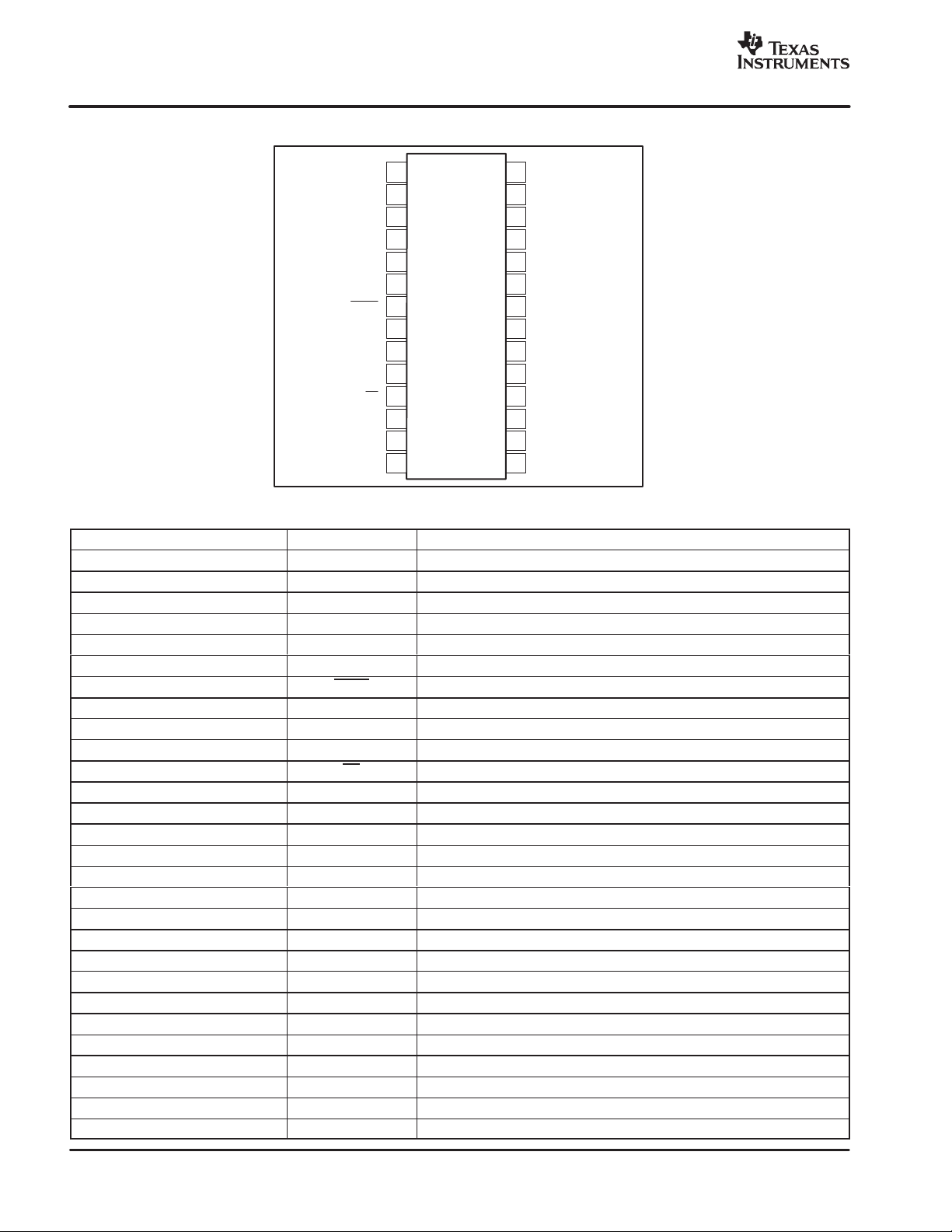
PIN CONFIGURATION
www.ti.com
PIN DESCRIPTIONS
PIN NUMBER NAME DESCRIPTION
1 GPO1 General-Purpose CMOS Logic Output
2 GPO2 General-Purpose CMOS Logic Output
3 GPO3 General-Purpose CMOS Logic Output
4 GPO4 General-Purpose CMOS Logic Output
5 OVR Over Range Output (Active High)
6 DGND Digital Ground
7 DCEN DC Servo Enable (Active Low)
8 0dB Unity Gain Enable (Active High)
9 ZCEN Zero Crossing Detector Enable (Active High)
10 SDI Serial Data Input
11 CS Chip Select Input (Active Low)
12 SCLK Serial Data Clock Input
13 SDO Serial Data Output
14 VD− −5V Digital Supply
15 VA− −5V Analog Supply
16 V
17 V
18 VA+ +5V Analog Supply
19 VA+ +5V Analog Supply
20 VA− −5V Analog Supply
21 C
22 C
23 C
24 C
25 V
26 VIN− Analog Input, Inverting
27 VIN+ Analog Input, Noninverting
28 AGND Analog Ground
1
GPO1
2
GPO2
3
GPO3
4
GPO4
5
OVR
6
DGND
7
DCEN
0dB
ZCEN
SDI
CS
SCLK
SDO
−
VD
− Analog Output, Inverting
OUT
+ Analog Output, Non-Inverting
OUT
S22
S21
S12
S11
IN Common Mode Voltage Input, 0V to +2.5V
COM
PGA2500
8
9
10
11
12
13
14
DC Servo Capacitor #2, Terminal 2
DC Servo Capacitor #2, Terminal 1
DC Servo Capacitor #1, Terminal 2
DC Servo Capacitor #1, Terminal 1
28
AGND
27
V
+
IN
−
26
V
IN
25
V
IN
COM
24
C
S11
23
C
S12
22
C
S21
21
C
S22
−
20
VA
19
VA+
18
VA+
17
V
+
OUT
−
16
V
OUT
−
15
VA
4
www.ti.com
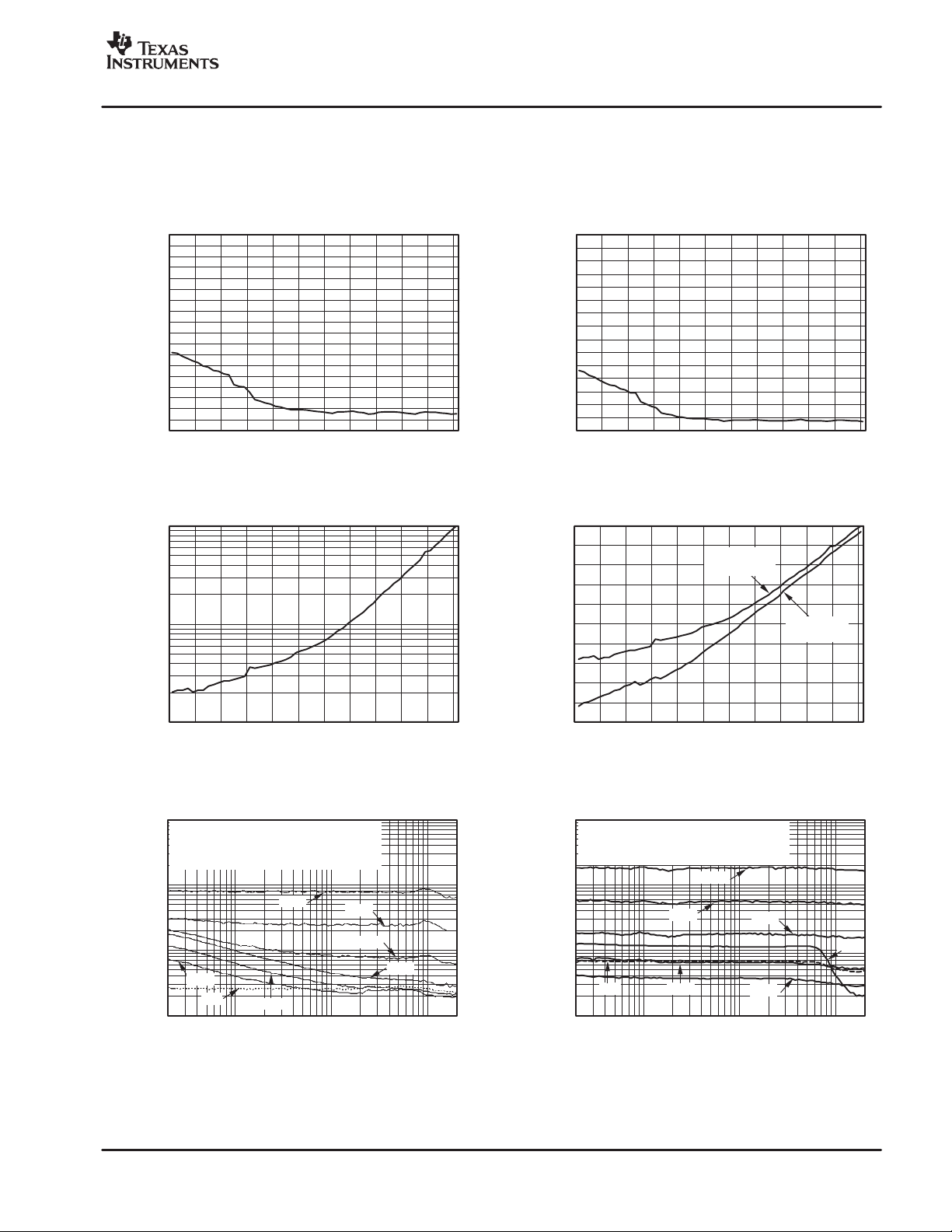
EQUIVALENT INPUT NOISE (E.I.N.) AS A FUNCTION OF GAIN
THD+N vs GAIN
THD+N vs FREQUENCY
EQUIVALENT INPUT NOISE (E.I.N.) AS A FUNCTION OF GAIN
THD+N AND NOISE vs GAIN
THD+N vs FREQUENCY
TYPICAL CHARACTERISTICS
All specifications at TA = +25°C, VA+ = +5V, VA− = −5V, VD− = −5V, and V
SBOS289A − NOVEMBER 2003 − REVISED DECEMBER 2003
IN = 0V , unless otherwise noted.
COM
"#$%%
−
100
−
102
−
104
−
106
−
108
−
110
−
112
−
114
−
116
−
118
−
120
−
122
E.I.N. (dBu)
−
124
−
126
−
128
−
130
−
132
−
134
−
136
10 15 20 25 30 35 40 45 50 55 60 65
Gain (dB)
(with Z = 0Ω)
0.01
(with 4.0 V
Output and Z = 40Ω)
RMS
0.001
THD+N (%)
0.0001
10 15 20 25 30 35 40 45 50 55 60 65
Gain (dB)
−
100
−
102
−
104
−
106
−
108
−
110
−
112
−
114
−
116
−
118
E.I.N. (dBu)
−
120
−
122
−
124
−
126
−
128
−
130
10 15 20 25 30 35 40 45 50 55 60 65
Gain (dB)
(with Z = 150Ω)
−
(0dB = 4V
80
−
85
−
90
−
95
−
100
−
105
−
110
−
115
THD+N and Noise (dB)
−
120
−
125
−
130
)
RMS
THD+N
with Z = 40
Ω
10 15 20 25 30 35 40 45 50 55 60 65
Gain Set (dB)
Noise
with Z = 0
Ω
(RS=40Ω,RL=600Ω,V
0.1
V
= 4.0Vrms Differential
OUT
for Gains = 10, 20, 30, 40, 50, and 60dB
= 3.5Vrms Differential for Gain = 0dB
V
OUT
IN=0V,BW=22Hzto22kHz)
COM
0.01
60dB
0.001
THD+N Ratio (%)
0.0001
10dB
0dB
20dB
20 100 1k 10k 20k
50dB
40dB
Frequency (Hz)
30dB
(RS=40Ω,RL= 600Ω,V
0.1
V
= 2.0Vrms Differential
OUT
for Gains = 10, 20, 30, 40, 50, and 60dB
= 1.0Vrms Differential for Gain = 0dB
V
OUT
0.01
0.001
THD+N Ratio (%)
0dB
0.0001
20 100 1k 10k 20k
IN = +2.5V, BW = 22Hz to 22kHz)
COM
60dB
50dB
30dB
40dB
20dB
Frequency (Hz)
10dB
5
"#$%%
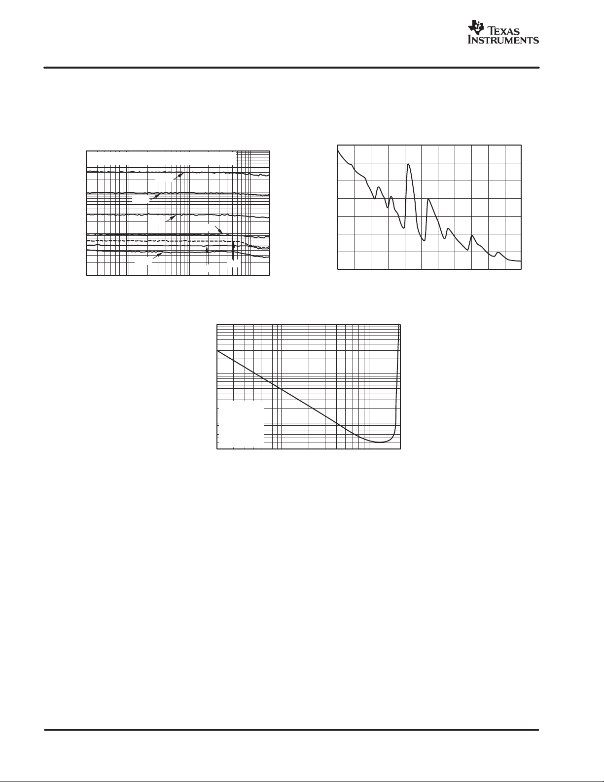
THD+N vs FREQUENCY
SBOS289A − NOVEMBER 2003 − REVISED DECEMBER 2003
TYPICAL CHARACTERISTICS (continued)
All specifications at TA = +25°C, VA+ = +5V, VA− = −5V, VD− = −5V, and V
IN = 0V , unless otherwise noted.
COM
www.ti.com
THD+N Ratio (%)
0.0001
(RS=40Ω,RL= 600Ω,V
0.1
V
= 1.0Vrms Differential for All Gain Settings
OUT
0.01
0.001
20 100 1k 10k 20k
50dB
10dB
IN = +2.5V, BW = 22Hz to 22kHz)
COM
60dB
40dB
Frequency (Hz)
30dB
20dB
0.1
0.01
THD+N (%)
0.0003
Gain = 30dB
f=1kHz
0.001
V
R
R
0.3 0.30 3.00 6.00
0dB
COM
S
L
THD+N vs OUTPUT AMPLITUDE
IN = 0V
Ω
=40
Ω
= 600
Output Amplitude (Vrms)
7
6
5
4
3
Bandwidth (MHz)
2
1
0
10 15 20 25 30 35 40 45 50 55 60 65
BANDWIDTH vs GAIN
Gain (dB)
6

www.ti.com
"#$%%
SBOS289A − NOVEMBER 2003 − REVISED DECEMBER 2003
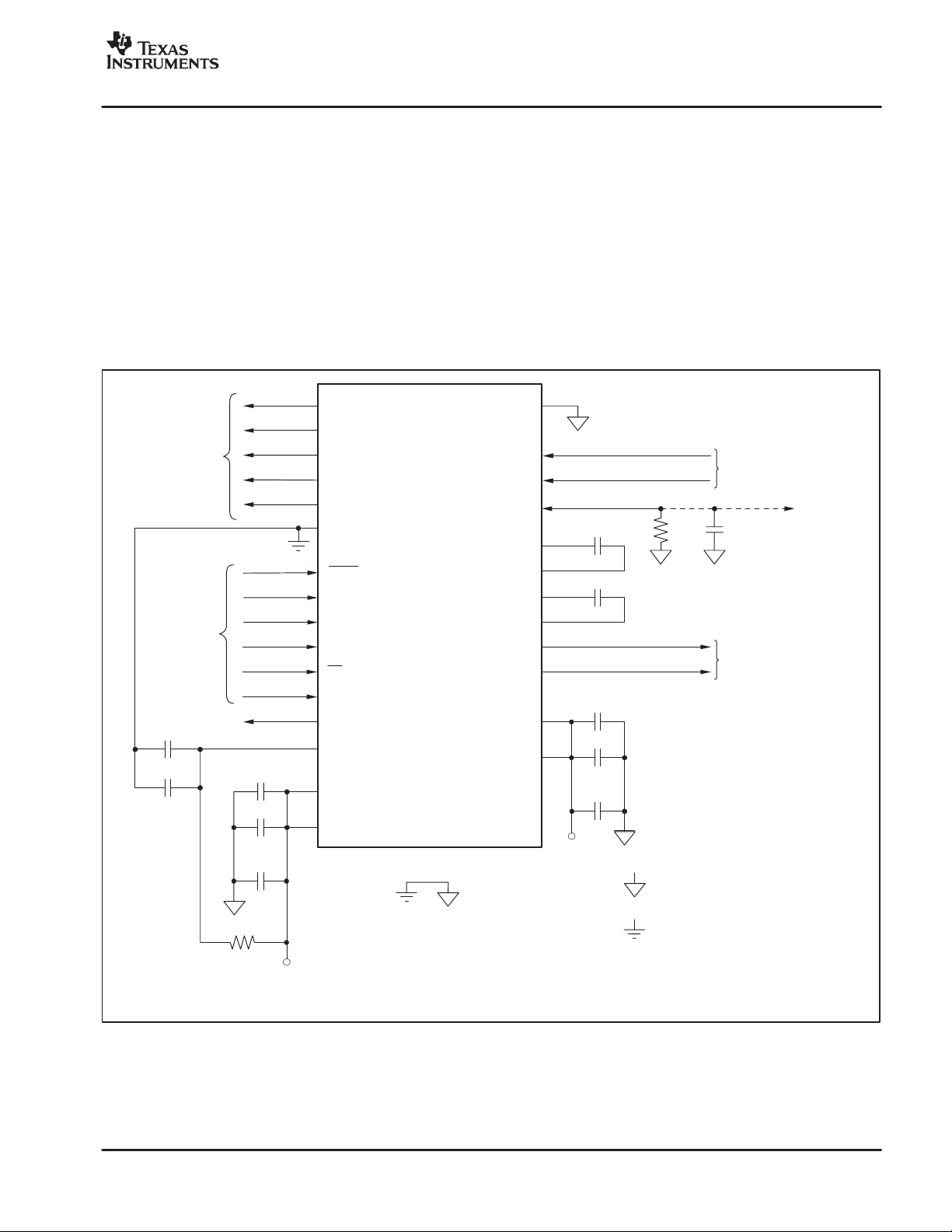
OVERVIEW
The PGA2500 is a digitally controlled microphone
preamplifier integrated circuit designed for amplifying the
output of dynamic and condenser microphones and
driving high performance audio analog-to-digital
converters (ADCs). A functional block diagram of the
PGA2500 is shown in Figure 1.
The analog input to the preamplifier is provided
differentially at the V
+ and VIN− inputs (pins 27 and 26,
IN
respectively). The programmable gain amplifier can be
programmed to either pass through the signal at unity gain,
or apply 10dB to 65dB of gain to the input signal. The gain
of the amplifier is adjustable over the full 10dB to 65dB
range in 1dB steps. The dif ferential output of the PGA2500
is made available at V
OUT
respectively). Gain is controlled using a serial port
interface.
ZCEN
GPO1
GPO2
GPO3
+ and V
0dB
− (pins 17 and 16,
OUT
SERIAL
PORT and
LOGIC
CONTROL
The four-wire serial port interface is used to program the
PGA2500 gain and support functions. A 16-bit control
word is utilized to program these functions (see Figure 2,
page 9). A serial data output pin provides support for
daisy-chaining multiple PGA2500 devices on a single
serial interface bus (see Figure 4, page 10).
The differential analog output of the PGA2500 is
constantly monitored by a DC servo amplifier loop. The
purpose of the servo loop is to minimize the DC offset
voltage present at the analog outputs by feeding back an
error signal to the input stage of the programmable gain
amplifier. The error signal is then used to correct the of fset.
The DC servo may be disabled by driving the DCEN
(pin 7) high or setting the DC
to 1. Normally, the DCEN
enable the DC servo, while the DC
bit in the serial control word
pin is connected to DGND to
bit is set to 0.
CS
SCLK
SDI
SDO
input
GPO4
V
IN
V
IN
AGND
VA+
VA+
VA
VA
OVR
IN
V
COM
V
+
+
−
Gain Range
0dB or
+10dB to +65dB
1dB per step
−
−
andCS2are external DC servointegratorcapacitors,
C
S1
and are connected across the C
PGA
C
S1
DC
Servo
C
S2
S11/CS12
and C
S21/CS22
pins, respectively.
OUT
V
OUT
−
VD
DGND
DCEN
−
Figure 1. PGA2500 Functional Block Diagram
7

"#$%%
SBOS289A − NOVEMBER 2003 − REVISED DECEMBER 2003
www.ti.com
Two external capacitors are required for the DC servo
function, with one capacitor connected between C
C
(pins 24 and 23), and the second capacitor connected
S12
between C
S21
and C
(pins 22 and 21). Capacitor values
S22
S11
and
up to 4.7µF may be utilized. However, larger valued
capacitors will result in longer settling times for the DC
servo loop. A value of 1µF is recommended for use in most
microphone preamplifier applications.
The PGA2500 includes a common-mode servo function.
This function is enabled and disabled using the CM bit in
the serial control word; see Figure 2. When enabled, the
servo provides common-mode negative feedback at the
input differential pair , resulting in very low common-mode
input impedance. The differential input impedance is not
affected by this feedback. This function is useful when the
source is floating, or has a high common-mode output
impedance. In this case, the only connection between the
source and the ground will be through the PGA2500
preamplifier input resistance.
In this case, input common-mode parasitic current is
determined by high output impedance of the source, not by
input impedance of the amplifier. Therefore, input
common-mode interference can be reduced by lowering
the common-mode input impedance while at the same
time not increasing the input common-mode current.
Increasing common-mode current degrades commonmode rejection. Using the common-mode servo, overall
common-mode rejection can be improved by suppressing
low and medium frequency common-mode interference.
The common-mode servo function is designed to operate
with a total common-mode input capacitance (including
the microphone cable capacitance) of up to 10nF. Beyond
this limit, stable servo operation is not ensured.
The common-mode voltage control input, named V
COM
IN
(pin 25), allows the PGA2500 output and input to be DCbiased to a common-mode voltage between 0 and +2.5V.
This allows for a DC-coupled interface between the
PGA2500 preamplifier output and the inputs of common
single-supply audio ADCs.
A dedicated 0dB input (pin 8) is provided so that the gain
of the PGA2500 may be forced to unity without using the
serial port interface. The 0dB input overrides gain settings
made through the serial port. While the 0dB input is active
(forced high), the serial port register may be updated or
data may passed through the serial interface to other
PGA2500 devices in daisy-chain configuration. However,
any changes made in the gain will not take effect until the
0dB input is driven low.
switching gain, thereby minimizing audible artifacts at the
preamplifier output. Since zero crossing detection can add
some delay when performing gain changes (up to 16ms
maximum for a detector timeout event), there may be
cases where the user may wish to disable the function.
Forcing the ZCEN input low disables zero crossing
detection, with gain changes occurring immediately when
programmed.
An overflow indicator output, OVR, is provided at pin 5.
The OVR pin is an active high, CMOS
-logic-level output.
The overflow output is forced high when the preamplifier
output voltage exceeds one of two preset thresholds. The
threshold is programmed through the serial port interface
using the OL bit. If OL = 0, then the threshold is set to
5.1V
differential, which is approximately −1dB below
RMS
the specified output voltage range. If OL = 1, then the
threshold is set to 4.0V
differential, which is
RMS
approximately −3dB below the specified output voltage
range.
The PGA2500 includes four programmable digital outputs,
named GPO1 through GPO4 (pins 1 through 4,
respectively), which are controlled via the serial port
interface. All four pins are CMOS
-logic-level outputs.
These pins may be used to control relay drivers or
switches used for external preamplifier functions,
including input pads, filtering, polarity reversal, or phantom
power.
ANALOG INPUTS AND OUTPUTS
An analog signal is input differentially across the VIN+ (pin
27) and V
input impedance are provided in the Electrical
Characteristics table. The Applications Information
section of this datasheet provides additional details
regarding typical input circuit considerations when
interfacing the PGA2500 to a microphone input.
Both V
below the common-mode input voltage, supplied at
V
COM
Figure 7, page 12) is highly recommended for the analog
inputs of the PGA2500. If DC
given application, the user must take this offset into
account.
It is recommended that a small capacitor be connected
from each analog input pin to analog ground. Values of at
least 50pF are recommended. See Figure 7 (page 12) for
larger capacitors being used for EMI filtering which will
satisfy this requirement.
− (pin 26) inputs. The input voltage range and
IN
+ and VIN− are biased at approximately 0.65V
IN
IN (pin 25). The use of AC-coupling capacitors (see
-coupling is required for a
The zero crossing control input, named ZCEN (pin 9), is
provided for enabling and disabling the internal zero
crossing detector function. Forcing the ZCEN input high
enables the function. Zero crossing detection is used to
force gain changes on zero crossings of the analog input
signal. This limits the glitch energy associated with
8
The analog output is presented differentially across V
(pin 17) and V
− (pin 16). The output voltage range is
OUT
OUT
provided in the Electrical Characteristics table. The analog
output is designed to drive a 600Ω differential load while
meeting the published THD+N specifications and typical
performance curves.
+

www.ti.com
"#$%%
SBOS289A − NOVEMBER 2003 − REVISED DECEMBER 2003
SERIAL PORT OPERATION
The serial port interface for the PGA2500 is comprised of
four wires: CS
SDO (pin 13). Figure 2 illustrates the serial port protocol,
while Figure 3 and the Electrical Characteristics table
provide detailed timing parameters for the port.
The CS
clock for the serial port. The CS
to clock data into and out of the serial port. The control
word is latched on a low-to-high transition of the CS input.
The serial port ignores the SCLK and SDI inputs when CS
is high, and the SDO output is set to a high impedance
state while CS
CS
SCLK
SDI
SDO
(pin 11), SCLK (pin 12), SDI (pin 10), and
input functions as the chip select and word latch
input must be low in order
is high.
Data Ignore d
High Impedance
DC Servo Enable
(Active Low)
CM Servo Enable
(Active High)
Overload Indicator Bit
(0 =5.1V
Data for GPO4
Data for GPO3
Data for GPO2
Data for GPO1
,1=4.0V
RMS
DC CM 0 OL D4 D3 D2 D1 0 0 G5 G4 G3 G2 G1 G0
DC CM 0 OL D4 D3 D2 D1 0 0 G5 G4 G3 G2 G1 G0
)
RMS
The SCLK input is used to clock serial data into the SDI pin
and out of the SDO pin. The SDI pin functions as the serial
data input, and is used to write the serial port register. Th e
SDO pin is the shift register serial output, and is used for
either register read-back or for daisy-chaining multiple
PGA2500 devices. Data on SDI is sampled on the rising
edge of SCLK, while data is clocked out of SDO on the
falling edge of SCLK.
When the 0dB input (pin 8) is forced high, the gain set by
the serial port register will be overridden. The serial port
register may be updated while the 0dB input is forced high,
but the programmed gain will not take effect until the 0dB
input is forced low.
DataIgnored
High Impedance
Preamplifier Gain
where N =G[5:0]
For N = 0
Gain =0dB
For N = 1 to 56
Gain (dB )= 9 + N
For N = 57 to63
Gain (dB )= 65
DEC
CS
SCLK
SDI
SDO
Figure 2. Serial Port Protocol
t
SDS
t
SDH
t
CSO
t
CSCR
MSB
MSB
t
CFDO
Figure 3. Serial Port Timing Requirements
t
CFCS
t
CSZ
9

"#$%%
SBOS289A − NOVEMBER 2003 − REVISED DECEMBER 2003
www.ti.com
DAISY-CHAINING MULTIPLE PGA2500 PREAMPLIFIERS
Since the serial port interface may be viewed as a serial in,
serial out shift register, multiple PGA2500 preamplifiers
may be connected in a cascaded or daisy-chained fashion,
as shown in Figure 4. The daisy-chained PGA2500
devices behave as a 16 x N-bit shift register, where N is the
V
+
OUT
−
V
OUT
V
+
IN
−
V
IN
V
+
OUT
−
V
OUT
V
+
IN
−
V
IN
PGA2500
#1
PGA2500
#2
SDI
CS
SCLK
SDO
SDI
CS
SCLK
SDO
number of cascaded PGA2500 devices. To program all of
the devices, simply force CS
low for 16 x N serial clock
periods and clock in 16 x N bits of control data. The CS
input is then forced high to latch in the new settings.
A timing diagram for the daisy-chain application is shown
in Figure 5.
DOUT
CS
DATACLK
DIN
Micro
or DSP
CS
SCLK
SDI
V
+
OUT
−
V
OUT
V
V
+
IN
−
IN
PGA2500
#N
SDI
CS
SCLK
SDO
Figure 4. Daisy-Chain Configuration for Multiple PGA2500 Preamplifiers
G0
DC G0DC
Device #2Device #N
DC G0
Figure 5. Serial Port Operation for Daisy-Chain Operation
Device #1
10
www.ti.com
"#$%%
SBOS289A − NOVEMBER 2003 − REVISED DECEMBER 2003
APPLICATION INFORMATION
This section provides practical information for designing
the PGA2500 into end applications.
BASIC CIRCUIT CONFIGURATION
A typical applications circuit, without the input and output
circuitry, is shown in Figure 6. Power-supply bypass and
DC servo capacitors are shown with recommended
values. All capacitors should be placed as close as
possible to the PGA2500 package to limit inductive noise
coupling. Surface-mount capacitors are recommended
(X7R ceramic for the 0.1µF and 1µF capacitors, and low
ESR tantalum for the 4.7µF capacitors).
1
GPO1
2
GPO2
3
GPO3
4
GPO4
5
OVR
6
DGND
7
DCEN
8
0dB
9
ZCEN
10
SDI
11
CS
12
SCLK
13
SDO
14
15
20
VD
VA
VA
−
−
−
PGA2500
Relay Drivers,
Switches, or Indicators
To/From
MPU, MCU,
DSP, or Logic
0.1µF
4.7µF
+
To
0.1µF
0.1µF
4.7µF
+
The PGA2500 can be placed on a split ground plane, with
the package located over the split. However, there must be
a low impedance connection between the analog and
digital grounds at a common return point.
The DC common-mode input, V
IN (pin 25), can be
COM
connected to analog ground or a DC voltage (such as the
reference or common voltage output of an audio ADC).
When biasing this input to a DC voltage, keep in mind that
both the analog output and input pins are level-shifted by
the value of the bias voltage.
VIN+
V
C
C
C
C
OUT
OUT
VA
VA
IN
S11
S12
S21
S22
28
27
26
−
25
IN
1µF
24
23
1µF
22
21
17
+
16
−
0.1µF
19
−
0.1µF
18
−
4.7µF
+
VA+
Ω
0
= Analog Ground
(1)
From
Analog Input
Circuit
(1)
0.1µF
To
Analog Output
Circuit
To
Optional
Common−Mode
Voltage
AGND
V
COM
V
V
Ω
10
VA
Connect Digital and Analog Grounds at
one common return point in the circuit.
−
NOTE: (1) Install a 0Ωshunt or jumper only when connecting V
to analog ground. Install a 0.1µF ceramic capacitor (X7R type) only
when connecting V
IN to a DC common−mode voltage source.
COM
= Digital Ground
COM
IN
Figure 6. Basic Circuit Configuration for the PGA2500
11
"#$%%
SBOS289A − NOVEMBER 2003 − REVISED DECEMBER 2003
www.ti.com
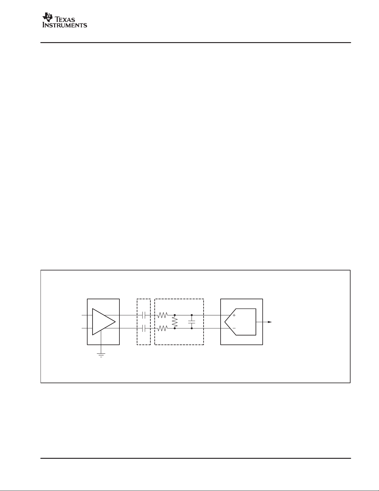
INPUT CIRCUIT CONSIDERATIONS
The input circuit for the PGA2500 must include several
items that are common to most microphone preamplifiers.
Figure 7 shows a typical input circuit configuration. Other
functions, such as input attenuation (pads), filters, and
polarity reversal switches are commonly found in
preamplifier circuits, but are not shown here in order to
focus on the basic input circuit requirements.
The microphone input is typically taken from a balanced
XLR or TRS input connection (XLR shown). The 1000pF
capacitors provide simple EMI filtering for the circuit.
Additional filtering for low- or high-frequency noise may be
added, depending upon the end application environment.
A bridging resistor is shown and may be selected to
provide the desired overall input impedance required for a
given microphone. This resistance will be in parallel with
the phantom power bias resistors and the PGA2500 input
resistance to set the actual impedance seen by the
microphone.
Connections for +48V phantom power, required for
condenser microphones, are shown in Figure 7. The
phantom power requires an On/Off switch, as dynamic
microphones do not require phantom power and may be
damaged if power is applied. DC-blocking capacitors are
required between the phantom power connections and the
PGA2500 inputs. The blocking capacitors are selected to
have a high working voltage rating, with 50V being the
minimum and 63V recommended for long term reliability.
The blocking capacitors, along with the PGA2500 input
resistance, form a high-pass filter circuit. With the typical
input resistance of the PGA2500 specified in the Electrical
Characteristics table, the value of the capacitor can be
chosen to meet the desired low frequency response for the
end application. At the same time, the value should be no
higher than required, since larger capacitors store more
charge and increase the surge current seen at the
preamplifier when a short circuit occurs on the microphone
input connector.
To protect the PGA2500 from large surge currents, power
Schottky diodes are placed on the input pins to both the
VA+ and VA− power supplies. Schottky diodes are used
due to their lower turn-on voltage compared to standard
rectifier diodes. Power devices are required since the
surge currents from a large valued blocking capacitor
(47µF) can exceed 4.5 amps for a very short duration of
time. It i s recommended that the Schottky diode chosen for
this application be specified for at least a 10A surge
current.
The use of a series current-limiting resistor prior to the
protection diodes will aid in handling surge currents,
although the resistor will add noise to the circuit. Select a
current-liming resistor value that is as high as tolerable for
the desired noise performance of the preamplifier circuit.
10µF−47µF
63WV
+
Ω
Phantom
Power
Switch
6.81k
0.25W
6.81k
0.25W
Ω
Mic Input
1
NOTES: (1) Bridging resistor, used to set the impedance seen by the microphone.
1000pF
2
1000pF
3
1000pF
+48V
(2) The blocking capacitor value is selected based upon the desired low frequency response.
(3) Current−limiting resistor. Select the highest value tolerable based upon input noise requirements.
(4) Schottky diode, selected for fast turn−on and rated for a minimum of a 10A surge current.
Recommended device is the MBRA120LT3 from ON Semiconductor.
(2)
(1)
10µF−47µF
63WV
+
(2)
(3)
VA+ VA
(3)
Figure 7. Typical Input Circuit for the PGA2500
(4) (4)
(4) (4)
V
+
IN
−
−
V
IN
12
www.ti.com
"#$%%
SBOS289A − NOVEMBER 2003 − REVISED DECEMBER 2003
OPERATION WITH V
COM
IN = +2.5V
When interfacing the analog outputs of the PGA2500 with
audio ADC inputs, the converter will frequently have a
common-mode DC output pin. This pin may be connected
to the V
IN pin of the PGA2500 in order to facilitate a
COM
DC-coupled interface between the two devices. The
common-mode DC voltage level is typically +2.5V,
although some converters may have a slightly lower value,
usually between +2.1V and +2.5V. There are several
issues that must be considered when operating the
PGA2500 in this fashion.
Both the analog input and output pins of the PGA2500 will
be level shifted by the V
will be shifted to the V
will be shifted to approximately V
IN voltage. The analog outputs
COM
IN level, while the analog inputs
COM
IN − 0.65V, due to the
COM
offset that normally exists on the input pins. The level
shifting will limit the input and output swing of the
PGA2500, reducing the overall signal-to-noise ratio and
degrading the THD+N performance.
Given V
IN = +2.5V and gains of 10dB through 65dB,
COM
the output swing is limited to less than one-half that
specified in the Electrical Characteristics table. The output
will hard-clip at approximately a diode drop below the VA+
supply rail and a diode drop above analog ground.
Given V
IN = +2.5V and a gain of 0dB, the practical
COM
maximum input or output voltage swing is approximately
1.0Vrms differential. Increasing the signal level much
beyond this point will result in a substantial increase in
distortion.
Plots of THD+N vs Frequency are shown in the Typical
Characteristics section of this datasheet for both
V
IN = 0V and +2.5V . The performance difference can
COM
be seen when comparing the plots. The user needs to
consider whether the difference is acceptable for the end
application.
As a suggested alternative, the PGA2500 analog outputs
may be AC-coupled to the ADC inputs, allowing the
PGA2500 to operate with V
IN = 0V in order to achieve
COM
best performance. The AC-coupling capacitors will affect
the overall low-frequency response of the preamplifier and
converter combination, and the user is advised to choose
a value that best suits the application requirements.
Figure 8 illustrates a typical PGA2500 to audio ADC
interface utilizing AC-coupling. In addition to the coupling
capacitors, a passive RC filter is required as an anti-alias
filter for the converter. The vast majority of audio ADCs are
of the oversampling delta-sigma variety, with a simple
single-pole filter meeting the anti-aliasing requirements for
this type of converter. Providing at least 6dB of attenuation
will also allow the PGA2500 to operate near full signal
swing without overdriving the ADC inputs.
Figure 9 illustrates an application where the V
COM
IN pin of
the PGA2500 is connected to the common-mode DC
output of the audio ADC, with a DC-coupled interface
between the PGA2500 analog outputs and the ADC
analog inputs.
PGA2500
PGA
V
COM
Coupling
Capacitors
C
C1
+
V
OUT
−
V
OUT
C
IN
NOTE: (1) PCM1804, PCM4202, or PCM4204.
R
+
+
C2
2R C
R
Attenuation and
Anti−Alias Filter
A/D Converter
ADC
(1)
Serial Data Output
PCM or DSD
Figure 8. PGA2500 Analog Output to ADC Analog Input Interface, AC-Coupled
13

"#$%%
SBOS289A − NOVEMBER 2003 − REVISED DECEMBER 2003
www.ti.com
ADC
COM
(1)
Serial Data Output
PCM or DSD
Output
0.1µF
PGA2500
R
+
V
OUT
PGA
−
V
OUT
R
IN V
V
COM
NOTE: (1) PCM1804, PCM4202, or PCM4204.
Anti−Alias Filter
C
A/D Converter
Figure 9. PGA2500 Analog Output to ADC Analog Input Interface, DC-Coupled
14
PACKAGE OPTION ADDENDUM
www.ti.com
6-Dec-2006
PACKAGING INFORMATION
Orderable Device Status
(1)
Package
Type
Package
Drawing
Pins Package
Qty
Eco Plan
PGA2500IDB ACTIVE SSOP DB 28 48 Green (RoHS &
no Sb/Br)
PGA2500IDBG4 ACTIVE SSOP DB 28 48 Green (RoHS &
no Sb/Br)
PGA2500IDBR ACTIVE SSOP DB 28 1000 Green (RoHS &
no Sb/Br)
PGA2500IDBRG4 ACTIVE SSOP DB 28 1000 Green (RoHS &
no Sb/Br)
(1)
The marketing status values are defined as follows:
ACTIVE: Product device recommended for new designs.
LIFEBUY: TI has announced that the device will be discontinued, and a lifetime-buy period is in effect.
NRND: Not recommended for new designs. Device is in production to support existing customers, but TI does not recommend using this part in
a new design.
PREVIEW: Device has been announced but is not in production. Samples may or may not be available.
OBSOLETE: TI has discontinued the production of the device.
(2)
Eco Plan - The planned eco-friendly classification: Pb-Free (RoHS), Pb-Free (RoHS Exempt), or Green (RoHS & no Sb/Br) - please check
http://www.ti.com/productcontent for the latest availability information and additional product content details.
TBD: The Pb-Free/Green conversion plan has not been defined.
Pb-Free (RoHS): TI's terms "Lead-Free" or "Pb-Free" mean semiconductor products that are compatible with the current RoHS requirements
for all 6 substances, including the requirement that lead not exceed 0.1% by weight in homogeneous materials. Where designed to be soldered
at high temperatures, TI Pb-Free products are suitable for use in specified lead-free processes.
Pb-Free (RoHS Exempt): This component has a RoHS exemption for either 1) lead-based flip-chip solder bumps used between the die and
package, or 2) lead-based die adhesive used between the die and leadframe. The component is otherwise considered Pb-Free (RoHS
compatible) as defined above.
Green (RoHS & no Sb/Br): TI defines "Green" to mean Pb-Free (RoHS compatible), and free of Bromine (Br) and Antimony (Sb) based flame
retardants (Br or Sb do not exceed 0.1% by weight in homogeneous material)
(2)
Lead/Ball Finish MSL Peak Temp
CU NIPDAU Level-2-260C-1 YEAR
CU NIPDAU Level-2-260C-1 YEAR
CU NIPDAU Level-2-260C-1 YEAR
CU NIPDAU Level-2-260C-1 YEAR
(3)
(3)
MSL, Peak Temp. -- The Moisture Sensitivity Level rating according to the JEDEC industry standard classifications, and peak solder
temperature.
Important Information and Disclaimer:The information provided on this page represents TI's knowledge and belief as of the date that it is
provided. TI bases its knowledge and belief on information provided by third parties, and makes no representation or warranty as to the
accuracy of such information. Efforts are underway to better integrate information from third parties. TI has taken and continues to take
reasonable steps to provide representative and accurate information but may not have conducted destructive testing or chemical analysis on
incoming materials and chemicals. TI and TI suppliers consider certain information to be proprietary, and thus CAS numbers and other limited
information may not be available for release.
In no event shall TI's liability arising out of such information exceed the total purchase price of the TI part(s) at issue in this document sold by TI
to Customer on an annual basis.
Addendum-Page 1

PACKAGE MATERIALS INFORMATION
www.ti.com
TAPE AND REEL INFORMATION
11-Mar-2008
*All dimensions are nominal
Device Package
PGA2500IDBR SSOP DB 28 1000 330.0 16.4 8.2 10.5 2.5 12.0 16.0 Q1
Type
Package
Drawing
Pins SPQ Reel
Diameter
(mm)
Reel
Width
W1 (mm)
A0 (mm) B0 (mm) K0 (mm) P1
(mm)W(mm)
Pin1
Quadrant
Pack Materials-Page 1
PACKAGE MATERIALS INFORMATION
www.ti.com
11-Mar-2008
*All dimensions are nominal
Device Package Type Package Drawing Pins SPQ Length (mm) Width (mm) Height (mm)
PGA2500IDBR SSOP DB 28 1000 346.0 346.0 33.0
Pack Materials-Page 2

MECHANICAL DATA
MSSO002E – JANUARY 1995 – REVISED DECEMBER 2001
DB (R-PDSO-G**) PLASTIC SMALL-OUTLINE
28 PINS SHOWN
0,65
28
1
2,00 MAX
0,38
0,22
15
14
A
0,05 MIN
0,15
5,60
5,00
M
8,20
7,40
Seating Plane
0,10
0,25
0,09
0°–ā8°
Gage Plane
0,25
0,95
0,55
PINS **
DIM
A MAX
A MIN
NOTES: A. All linear dimensions are in millimeters.
B. This drawing is subject to change without notice.
C. Body dimensions do not include mold flash or protrusion not to exceed 0,15.
D. Falls within JEDEC MO-150
14
6,50
6,50
5,905,90
2016
7,50
6,90
24
8,50
28
10,50
9,907,90
30
10,50
9,90
38
12,90
12,30
4040065 /E 12/01
POST OFFICE BOX 655303 • DALLAS, TEXAS 75265

IMPORTANT NOTICE
Texas Instruments Incorporated and its subsidiaries (TI) reserve the right to make corrections, modifications, enhancements, improvements,
and other changes to its products and services at any time and to discontinue any product or service without notice. Customers should
obtain the latest relevant information before placing orders and should verify that such information is current and complete. All products are
sold subject to TI’s terms and conditions of sale supplied at the time of order acknowledgment.
TI warrants performance of its hardware products to the specifications applicable at the time of sale in accordance with TI’s standard
warranty. Testing and other quality control techniques are used to the extent TI deems necessary to support this warranty. Except where
mandated by government requirements, testing of all parameters of each product is not necessarily performed.
TI assumes no liability for applications assistance or customer product design. Customers are responsible for their products and
applications using TI components. To minimize the risks associated with customer products and applications, customers should provide
adequate design and operating safeguards.
TI does not warrant or represent that any license, either express or implied, is granted under any TI patent right, copyright, mask work right,
or other TI intellectual property right relating to any combination, machine, or process in which TI products or services are used. Information
published by TI regarding third-party products or services does not constitute a license from TI to use such products or services or a
warranty or endorsement thereof. Use of such information may require a license from a third party under the patents or other intellectual
property of the third party, or a license from TI under the patents or other intellectual property of TI.
Reproduction of TI information in TI data books or data sheets is permissible only if reproduction is without alteration and is accompanied
by all associated warranties, conditions, limitations, and notices. Reproduction of this information with alteration is an unfair and deceptive
business practice. TI is not responsible or liable for such altered documentation. Information of third parties may be subject to additional
restrictions.
Resale of TI products or services with statements different from or beyond the parameters stated by TI for that product or service voids all
express and any implied warranties for the associated TI product or service and is an unfair and deceptive business practice. TI is not
responsible or liable for any such statements.
TI products are not authorized for use in safety-critical applications (such as life support) where a failure of the TI product would reasonably
be expected to cause severe personal injury or death, unless officers of the parties have executed an agreement specifically governing
such use. Buyers represent that they have all necessary expertise in the safety and regulatory ramifications of their applications, and
acknowledge and agree that they are solely responsible for all legal, regulatory and safety-related requirements concerning their products
and any use of TI products in such safety-critical applications, notwithstanding any applications-related information or support that may be
provided by TI. Further, Buyers must fully indemnify TI and its representatives against any damages arising out of the use of TI products in
such safety-critical applications.
TI products are neither designed nor intended for use in military/aerospace applications or environments unless the TI products are
specifically designated by TI as military-grade or "enhanced plastic." Only products designated by TI as military-grade meet military
specifications. Buyers acknowledge and agree that any such use of TI products which TI has not designated as military-grade is solely at
the Buyer's risk, and that they are solely responsible for compliance with all legal and regulatory requirements in connection with such use.
TI products are neither designed nor intended for use in automotive applications or environments unless the specific TI products are
designated by TI as compliant with ISO/TS 16949 requirements. Buyers acknowledge and agree that, if they use any non-designated
products in automotive applications, TI will not be responsible for any failure to meet such requirements.
Following are URLs where you can obtain information on other Texas Instruments products and application solutions:
Products Applications
Amplifiers amplifier.ti.com Audio www.ti.com/audio
Data Converters dataconverter.ti.com Automotive www.ti.com/automotive
DSP dsp.ti.com Broadband www.ti.com/broadband
Clocks and Timers www.ti.com/clocks Digital Control www.ti.com/digitalcontrol
Interface interface.ti.com Medical www.ti.com/medical
Logic logic.ti.com Military www.ti.com/military
Power Mgmt power.ti.com Optical Networking www.ti.com/opticalnetwork
Microcontrollers microcontroller.ti.com Security www.ti.com/security
RFID www.ti-rfid.com Telephony www.ti.com/telephony
RF/IF and ZigBee® Solutions www.ti.com/lprf Video & Imaging www.ti.com/video
Mailing Address: Texas Instruments, Post Office Box 655303, Dallas, Texas 75265
Copyright © 2008, Texas Instruments Incorporated
Wireless www.ti.com/wireless
 Loading...