

Page 1

User's Guide
SBOU073A–February 2009–Revised May 2012
PGA112EVM and PGA113EVM User’s Guide
This user's guide describes the characteristics, operation, and use of the PGA112EVM and PGA113EVM
evaluation boards. It also describes how to set up and configure the software and hardware, and reviews
various aspects of program operation. Throughout this document, the terms PGA112EVM, PGA113EVM,
PGA112EVM/PGA113EVM, evaluation board, evaluation module, and EVM are synonymous with the
PGA112EVM and PGA113EVM. This user's guide also includes information regarding operating
procedures and input/output connections, an electrical schematic, printed circuit board (PCB) layout
drawings, and a parts list for the EVM.
Contents
1 Overview ..................................................................................................................... 2
2 EVM Hardware Setup ...................................................................................................... 3
3 EVM Hardware Overview .................................................................................................. 5
4 EVM Software Setup ....................................................................................................... 7
5 EVM Software Overview ................................................................................................... 9
6 EVM Documentation ...................................................................................................... 13
List of Figures
1 Hardware Setup............................................................................................................. 3
2 EVM Block Diagram ........................................................................................................ 3
3 SM-USB-DIG Platform Block Diagram................................................................................... 4
4 Typical EVM Hardware Connections..................................................................................... 5
5 Confirmation of SM-USB-DIG Platform Driver Installation............................................................. 5
6 PGA112EVM Hardware (Note that the PGA113EVM is identical except for the device name).................. 6
7 EVM Installer Files.......................................................................................................... 7
8 Install Path................................................................................................................... 8
9 EVM Software Interface.................................................................................................... 9
10 Communication Error with SM-USB-DIG Platform.................................................................... 10
11 Read, Write, and Auto-Write Buttons................................................................................... 10
12 Individual Bits Panel and Help w Reg Button.......................................................................... 11
13 Setting DVDD Voltage .................................................................................................... 11
14 Input Mux Configuration .................................................................................................. 12
15 Setting the Gain ........................................................................................................... 12
16 EVM Schematic............................................................................................................ 14
17 PCB Component Layout.................................................................................................. 15
List of Tables
1 Contents of PGA112EVM or PGA113EVM Kit.......................................................................... 2
2 SM-USB-DIG Pin Definitions .............................................................................................. 4
3 EVM Bill of Materials ..................................................................................................... 13
Windows, Windows XP are trademarks of Microsoft Corporation.
I2C is a trademark of NXP Semicinductors.
All other trademarks are the property of their respective owners.
SBOU073A–February 2009–Revised May 2012 PGA112EVM and PGA113EVM User’s Guide
Submit Documentation Feedback
Copyright © 2009–2012, Texas Instruments Incorporated
1
Page 2
Overview
1 Overview
The PGA112 And PGA113 are programmable gamma-voltage generators featuring two banks of 16
programmable gamma channels and programmable, high slew rate VCOM channels. All channels are
programmable through a high-speed, I2C™ interface and support up to 20-V supply-voltage operation.
1.1 EVM Kit Contents
Table 1 lists the contents of the PGA112EVM or PGA113EVM kit. Contact the Texas Instruments Product
Information Center nearest you if any component is missing. It is highly recommended that you check the
TI web site at http://www.ti.com to verify that you have the latest versions of the related software.
Table 1. Contents of PGA112EVM or PGA113EVM Kit
Item Quantity
PGA112EVM or PGA113EVM PCB Evaluation Board 1
SM-USB-DIG Platform PCB 1
USB Extender Cable 1
SM-USB-DIG Connector Ribbon Cable 1
User’s Guide CD-ROM 1
1.2 Related Documentation from Texas Instruments
The following document provides information regarding Texas Instruments integrated circuits used in the
assembly of the PGA112EVM and PGA113EVM. This user's guide is available from the TI web site under
literature number SBOU073. Any letter appended to the literature number corresponds to the document
revision that is current at the time of the writing of this document. Newer revisions may be available from
the TI web site at http://www.ti.com/, or call the Texas Instruments Literature Response Center at (800)
477-8924 or the Product Information Center at (972) 644-5580. When ordering, identify the document by
both title and literature number.
www.ti.com
Document Literature Number
PGA112/PGA113 Product Data Sheet SBOS424
SM-USB-DIG Platform User's Guide SBOU098
2
PGA112EVM and PGA113EVM User’s Guide SBOU073A–February 2009–Revised May 2012
Copyright © 2009–2012, Texas Instruments Incorporated
Submit Documentation Feedback
Page 3
www.ti.com
2 EVM Hardware Setup
This section describes the overall system setup for the PGA112EVM and PGA113EVM. The SM-USB-DIG
Platform provides power and the digital signals used to communicate with the PGA112EVM or
PGA113EVM board through software installed on your PC. An input signal and multimeter can be
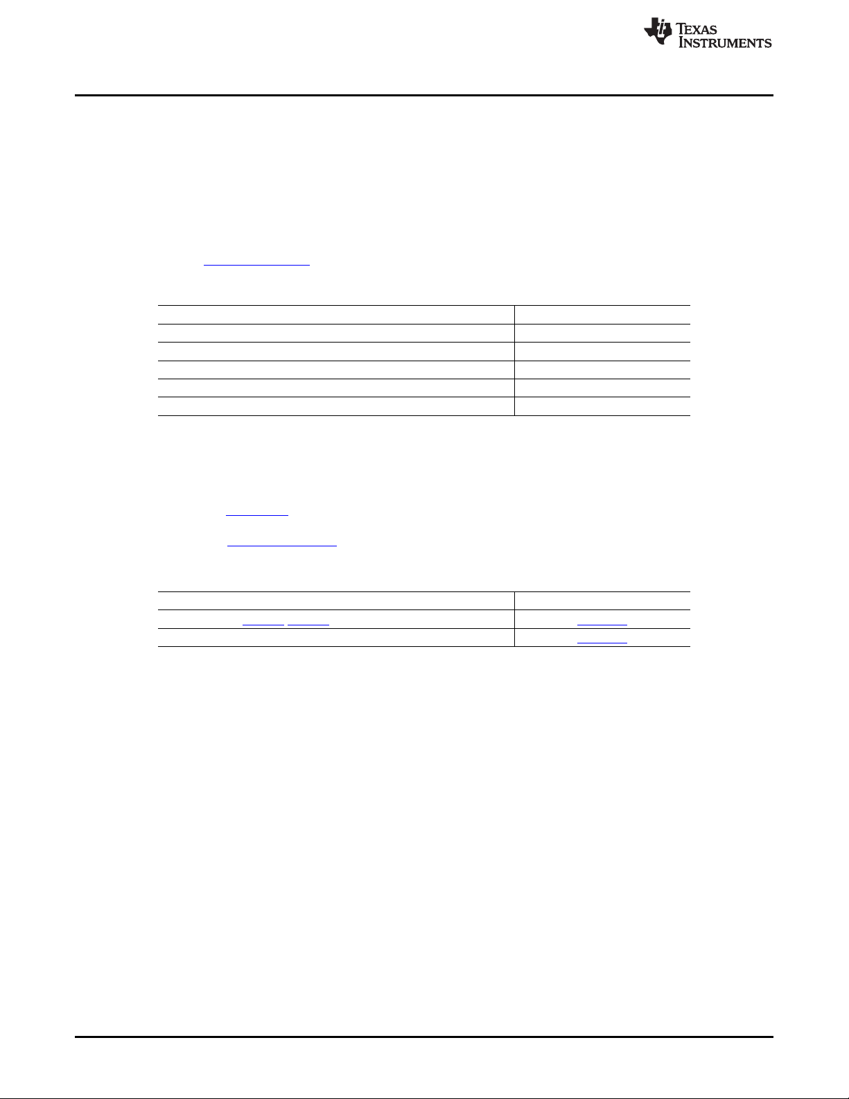
attached to the available connectors on the PGA112EVM and PGA113EVM boards. Figure 1 shows the
hardware setup.
EVM Hardware Setup
Figure 1. Hardware Setup
2.1 Theory of Operation for the PGA112 and PGA113 Hardware
A block diagram of the test-board hardware setup is shown in Figure 2. The EVM board provides test
points to the communication inputs. The EVM board also provides power and ground connections (from
the SM-USB-DIG Platform board or an external power supply; see Section 3.4). The EVM board also
provides test points for the analog inputs and output of the PGA112 (or PGA113) device. The
PGA112EVM and PGA113EVM feature a test point for the VREF input of the PGA112 and PGA113,
respectively. By default, VREF is shorted to ground, but can be disconnected with the removal of R2.
Figure 2. EVM Block Diagram
SBOU073A–February 2009–Revised May 2012 PGA112EVM and PGA113EVM User’s Guide
Submit Documentation Feedback
Copyright © 2009–2012, Texas Instruments Incorporated
3
Page 4
TUSB3210
8052 mC
w/USB Interface
and UART
USB Bus
from
Computer
3.3-V
Regulator
+3.3 V
USB
+5.0 V
8K x 8 Byte
EEPROM
Buffers and
Level
Translators
Power
Switching
Vdut
(Hi-Z, 3.3 V, or 5 V)
Switched Power
I2C
SPI
Control Bits
Measure Bits
Power on
Reset
SM-USB-DIG Platform
To Test Board
To Computer and Power Supplies
+3.3 V
USB +5.0 V
EVM Hardware Setup
2.2 Signal Definitions of J1 (10-Pin Male Connector Socket)
Table 2 shows the pin out for the 10-pin connector socket used to communicate between the EVM and the
SM-USB-DIG. Note that the EVM uses only the I2C communication lines, VDUT (pin 6), GND (pin 8), and
CTRL/MEAS4 (pin 2).
Table 2. SM-USB-DIG Pin Definitions
Pin on U1 Signal Description
1 I2C_SCL I2C clock signal (SCL)
2 CTRL/MEAS4 GPIO. Control output or measure input
3 I2C_SDA1 I2C data signal (SDA)
4 CTRL/MEAS5 GPIO. Control output or measure input
5 SPI_DOUT1 SPI data output (MOSI)
6 VDUT
7 SPI_CLK SPI clock signal (SCLK)
8 GND Power return (GND)
9 SPI_CS1 SPI chip select signal (CS)
10 SPI_DIN1 SPI data input (MISO)
Switchable DUT power supply: +3.3 V, +5 V, Hi-Z (disconnected).
NOTE: When VDUT is Hi-Z, all digital I/O are also Hi-Z.
2.3 Theory of Operation for SM-USB-DIG Platform
www.ti.com
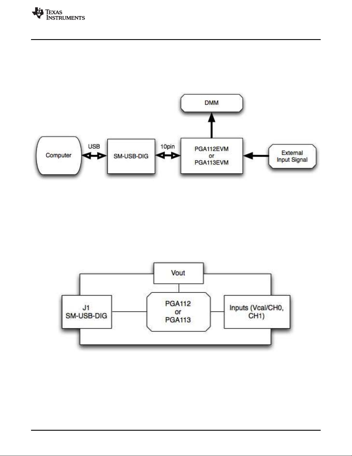
Figure 3 shows the block diagram for the SM-USB-DIG Platform. This platform is a general-purpose data
acquisition system that is used on several different Texas Instruments evaluation modules. The details of
its operation are included in the SM-USB-DIG Platform User's Guide (SBOU098). The block diagram
shown in Figure 3 is given as a brief overview of the platform.
Figure 3. SM-USB-DIG Platform Block Diagram
The primary component of the SM-USB-DIG Platform is the TUSB3210, an 8052 microcontroller with a
built-in USB interface. The microcontroller receives information from the host computer that is interpreted
into power, I2C, SPI, and other digital I/O methods. During the digital I/O transaction, the microcontroller
reads the response of any device connected to the I/O interface. The response from the device is sent
back to the PC, where it is interpreted by the host computer.
4
PGA112EVM and PGA113EVM User’s Guide SBOU073A–February 2009–Revised May 2012
Copyright © 2009–2012, Texas Instruments Incorporated
Submit Documentation Feedback
Page 5
www.ti.com
3 EVM Hardware Overview
Using the PGA112EVM or PGA113EVM hardware requires connecting the SM-USB-DIG Platform and the
EVM together, applying power, connecting the USB cable, and providing the input signal. This section
presents the details of these procedures.
3.1 Electrostatic Discharge Warning
Many of the components on the PGA112EVM and PGA113EVM are susceptible to damage by
electrostatic discharge (ESD). Customers are advised to observe proper ESD handling precautions when
unpacking and handling the EVM, including the use of a grounded wrist strap at an approved ESD
workstation.
3.2 Connecting the Hardware
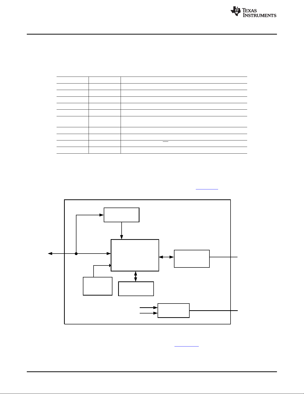
To connect the EVM board and the SM-USB-DIG Platform together, firmly slide the male and female ends
of the 10-pin connectors together, as shown in Figure 4. Make sure that the two connectors are
completely pushed together; loose connections may cause intermittent operation.
EVM Hardware Overview
Figure 4. Typical EVM Hardware Connections
3.3 Connecting the USB Cable to the SM-DIG-Platform
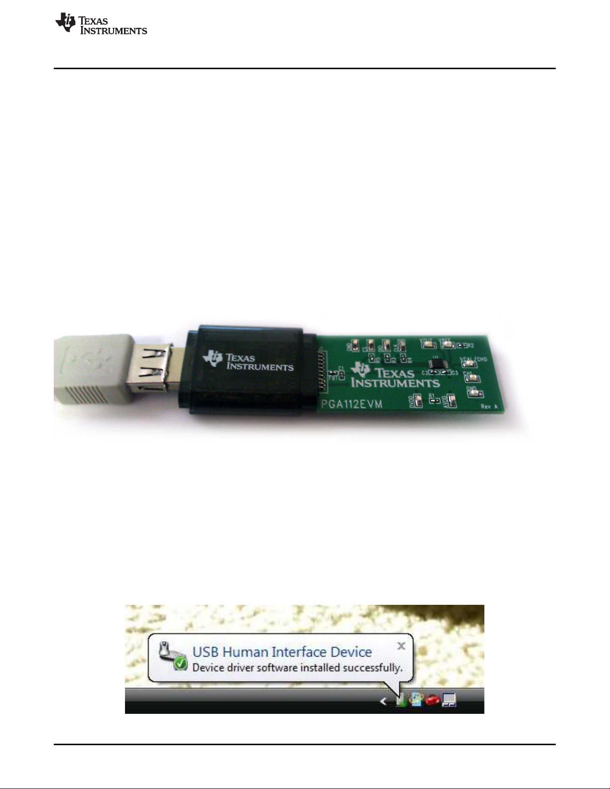
Figure 5 shows the typical response when connecting the SM-USB-DIG Platform board to a PC USB port
for the first time. Typically, the computer responds with a Found New Hardware, USB Device pop-up
dialog. The pop-up window then usually changes to Found New Hardware, USB Human Interface Device.
This pop-up indicates that the device is ready to be used. The SM-USB-DIG Platform uses the human
interface device drivers that are part of the Microsoft Windows™ operating system.
Figure 5. Confirmation of SM-USB-DIG Platform Driver Installation
SBOU073A–February 2009–Revised May 2012 PGA112EVM and PGA113EVM User’s Guide
Submit Documentation Feedback
Copyright © 2009–2012, Texas Instruments Incorporated
5
Page 6

EVM Hardware Overview
In some cases, the Windows Add Hardware Wizard starts. If this prompt appears, allow the system device
manager to install the human interface drivers by clicking Yes when requested to install drivers.
3.4 Powering the EVM
By default, a 0-Ω resistor (R1) is used to short DVDD and AVDD together, with both being supplied by the
SM-USB-DIG Platform. If a different supply is desired for AVDD, R1 can be removed and the supply can
be connected to the AVDD and GND test points. The SM-USB-DIG Plartform can supply 5 V or 3.3 V to
the EVM.
3.5 EVM Features
This section describes some of the hardware features present on the PGA112EVM and PGA113EVM
boards. Note that these two EVMs are identical except for the device name.
3.5.1 Communication Test Points
The PGA112EVM and PGA113EVM boards feature test points (CS, DIO, and CLK) for monitoring
communication between the SM-USB-DIG Platform and the PGA112 (or PGA113) device, as shown in
Figure 6. The test points allow external signals to be connected if the EVM is integrated into a custom
application or prototype. Note that if the SM-USB-DIG Platofrm is not being used, an external power
source must be connected to DVDD and AVDD.
www.ti.com
(Note that the PGA113EVM is identical except for the device name)
3.5.2 Output Test Points
Test point VOUT is used for measuring the output of the EVM.
3.5.3 Voltage Reference
For simplicity, the VREF input of the EVM is shorted to ground through 0-Ω resistor R2 by default. If a
different VREF is desired, R2 can be removed.
3.5.4 Analog Input Signals
Test points VCAL/CH0 and CH1 are used for connecting the input signals to the EVM, as shown in
Figure 6.
6
PGA112EVM and PGA113EVM User’s Guide SBOU073A–February 2009–Revised May 2012
Figure 6. PGA112EVM Hardware
Copyright © 2009–2012, Texas Instruments Incorporated
Submit Documentation Feedback
Page 7

www.ti.com
4 EVM Software Setup
This section discusses how to install the EVM software.
4.1 Operating Systems for EVM Software
The EVM software has been tested on the Microsoft Windows XP™ operating system (OS) with United
States and European regional settings. The software should also function on other Windows operating
systems.
4.2 Software Installation
The EVM software is included on the CD that is shipped with the EVM kit. It is also available through the
PGA112EVM or PGA113EVM product folder on the TI web site. To install the software to your system,
insert the disc into an available CD-ROM drive and navigate to the drive contents. Locate the compressed
file (PGA112-113EVM-Software), open it, find the setup.exe file (as shown in Figure 7), and run it to start
the installation. The PGA112-113EVM software installer then begins the installation process.
EVM Software Setup
Figure 7. EVM Installer Files
SBOU073A–February 2009–Revised May 2012 PGA112EVM and PGA113EVM User’s Guide
Submit Documentation Feedback
Copyright © 2009–2012, Texas Instruments Incorporated
7
Page 8

EVM Software Setup
After the install initializes, choose the directory where the program is installed; usually, the default
directory is C:\Program Files\PGA112-113EVM\ and C:\Program Files\National Instruments\, as shown in
Figure 8. Following this step, two license agreements are presented that must be accepted. After
accepting the Texas Instruments and National Instruments license agreements, the progress bar opens
and shows the installation of the software. After the installation process is completed, click Finish.
www.ti.com
Figure 8. Install Path
8
PGA112EVM and PGA113EVM User’s Guide SBOU073A–February 2009–Revised May 2012
Copyright © 2009–2012, Texas Instruments Incorporated
Submit Documentation Feedback
Page 9

www.ti.com
5 EVM Software Overview
This section describes how to use the EVM software.
5.1 Starting the EVM Software
The EVM software can be operated through the Start menu in Windows. From the Start menu, select All
Programs, and then select the PGA112-113EVM program. Figure 9 illustrates how the software should
appear at launch if the PGA112EVM (or PGA113EVM) is functioning properly.
EVM Software Overview
Figure 9. EVM Software Interface
SBOU073A–February 2009–Revised May 2012 PGA112EVM and PGA113EVM User’s Guide
Submit Documentation Feedback
Copyright © 2009–2012, Texas Instruments Incorporated
9
Page 10

EVM Software Overview
Figure 10 shows the error that appears if the computer cannot communicate with the EVM. In the event
you receive this error, first ensure that the both ends of the USB cable are properly connected. This error
can also occur if you connect the USB cable before the EVM is powered on (if using an external supply as
described in Section 3.4). Another possible source for this error is a problem with your computer USB
human interface device (HID) driver. Make sure that the device is recognized when the USB cable is
plugged in, indicated by a Windows-generated confirmation sound.
Figure 10. Communication Error with SM-USB-DIG Platform
5.2 EVM Software Features
5.2.1 Selecting Correct EV
The EVM software can be configured to communicate to either the PGA112EVM or the PGA113EVM. The
Part Type selection field is used to select the correct device, as shown in Figure 11. This setting is
automatically saved.
www.ti.com
Figure 11. Read, Write, and Auto-Write Buttons
5.2.2 Reading and Writing to Registers
The EVM software only reads and writes to the PGA112 (or PGA113) registers at the user’s command.
This is accomplished with the Read All Reg and Write All Reg buttons, as shown in Figure 11. When any
change is made to the configuration register, the green light is lit to show that changes are pending.
Pressing the Write All Reg button writes the pending changes to the PGA112 (or PGA113). In addition, by
enabling the Auto-Write button, changes are written to the configuration register automatically.
The PGA112 is read only when the Read All Reg button is pressed. To verify that the PGA112 (or
PGA113) successfully stored the data, read from the device after writing to the configuration register.
10
PGA112EVM and PGA113EVM User’s Guide SBOU073A–February 2009–Revised May 2012
Copyright © 2009–2012, Texas Instruments Incorporated
Submit Documentation Feedback
Page 11
www.ti.com
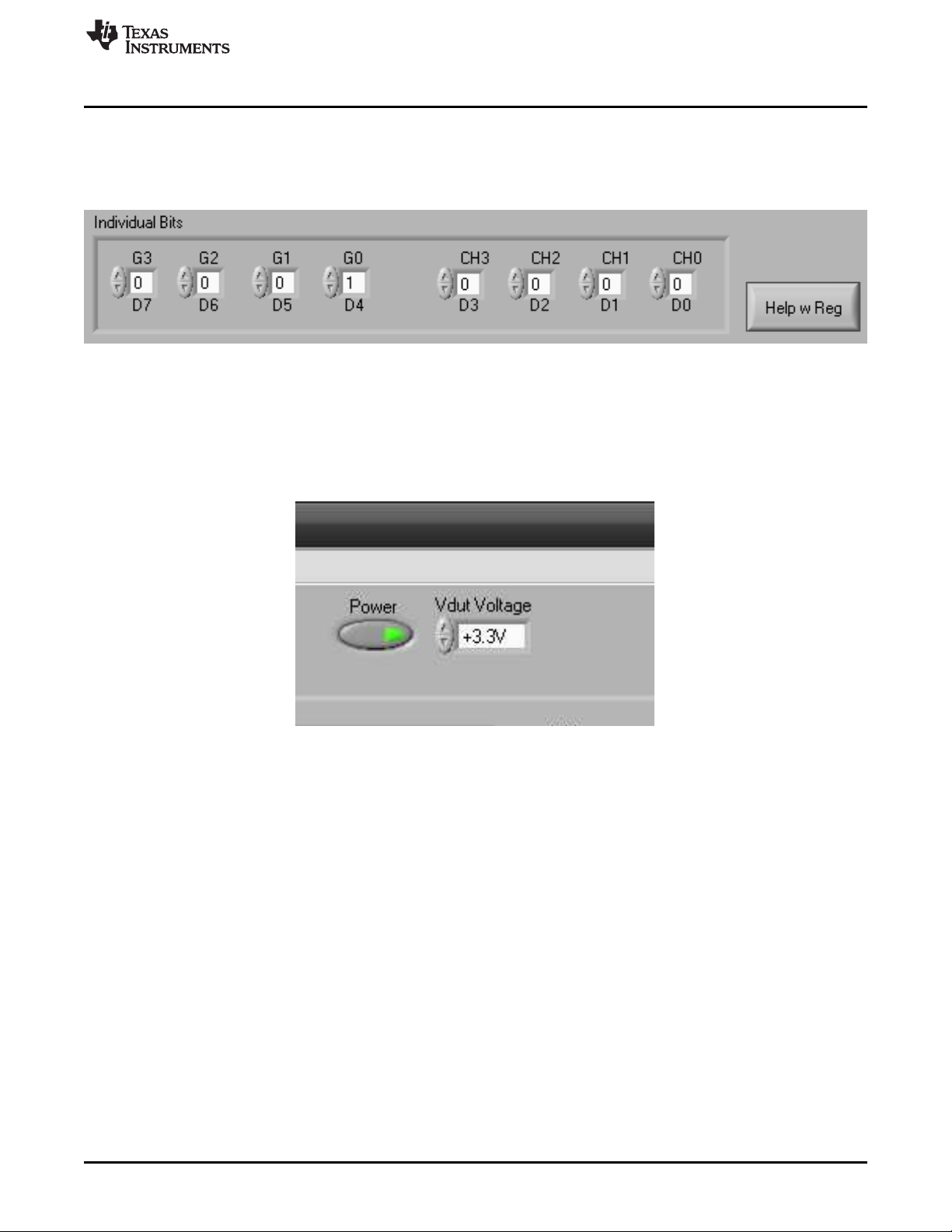
5.2.3 Setting Individual Bits
Use the Individual Bits panel to set the individual bits of the PGA112 (or PGA113) configuration register.
The panel, shown in Figure 12, has a settable bank for all bits in the register. Press the Help w Reg button
for information about the register.
Figure 12. Individual Bits Panel and Help w Reg Button
5.2.4 Setting DVDD and AVDD
The SM-USB-DIG Platform supports two logic-level voltages: 3.3 V and 5 V. Set the voltage by using the
Vdut Voltage menu, as shown in Figure 13. Disable the voltage from the SM-USB-DIG Platform by
toggling the Power button.
EVM Software Overview
Figure 13. Setting DVDD Voltage
SBOU073A–February 2009–Revised May 2012 PGA112EVM and PGA113EVM User’s Guide
Submit Documentation Feedback
Copyright © 2009–2012, Texas Instruments Incorporated
11
Page 12

EVM Software Overview
5.2.5 Setting the Input Multiplexer
The input multiplexer (mux) of the PGA112 (or PGA113) device can be set by the Input Mux drop-down
menu shown in Figure 14. External test points VCAL/CH0 and CH1 can be selected in this menu, as well
as the various calibration inputs.
www.ti.com
5.2.6 Setting Gain
Use the Gain drop-down menu shown in Figure 15 to configure the PGA112 (or PGA113) device gain
value.
Figure 14. Input Mux Configuration
Figure 15. Setting the Gain
12
PGA112EVM and PGA113EVM User’s Guide SBOU073A–February 2009–Revised May 2012
Copyright © 2009–2012, Texas Instruments Incorporated
Submit Documentation Feedback
Page 13

www.ti.com
EVM Documentation
6 EVM Documentation
This section contains the complete bill of materials, schematic diagram, and PCB layout for the PGA112EVM and PGA113EVM. Documentation
information for the SM-USB-DIG Platform can be found in the SM-USB-DIG Platform User’s Guide, SBOU098, available for download at
www.ti.com.
6.1 PGA112EVM and PGA113 Bill of Materials
Table 3 lists the bill of materials for both the PGA112EVM and PGA113EVM test boards.
Table 3. EVM Bill of Materials
Quantity Value Ref Des Description Vendor Part Number
PGA112EVM and PGA113EVM
1 N/A J1 CONN SOCKET 10PIN .050 R/A SNGL Mill-Max Manu. Corp. 851-43-010-20-001000
2 N/A 1, 2 BUMPON CYLINDRICAL .375X.135 BLK 3M SJ61A8
11 N/A CLK, CS, DIO, DVDD, TEST POINT, MINIATURE Keystone Electronics 5015
3 0.1 µF C1, C2, C3 CAPACITOR CER .1UF 16V, 0402 Murata Electronics North America GRM155R71C104KA88D
2 0 Ω R1, R2 RESISTOR, 0Ω, 0402 Yageo RC0402JR-070RL
3 10 kΩ R3, R4, R5 RESISTOR, 10KΩ, 0402, 1/16W, 5% Yageo RC0402JR-0710KL
1 N/A FB1 FERRITE BEAD, 300Ω, .2A, 0402 Wurth 74279272
PGA112EVM Only
1 N/A U1 PG112, Zero-Drift, Programmable Gain Amplifier with MUX, MSOP-10 Texas Instruments PGA112AIDGSR
PGA113EVM Only
1 N/A U1 PGA113, Zero-Drift, Programmable Gain Amplifier with MUX, MSOP-10 Texas Instruments PGA113AIDGSR
AVDD, CH1, VCAL/CH0,
VOUT, VREF, GND(x2)
SBOU073A–February 2009–Revised May 2012 PGA112EVM and PGA113EVM User’s Guide
Submit Documentation Feedback
Copyright © 2009–2012, Texas Instruments Incorporated
13
Page 14

EVM Documentation
6.2 EVM Schematic
Figure 16 shows the schematic for the PGA112EVM. Note that the PGA113 schematic is identical except for the device name.
www.ti.com
Figure 16. EVM Schematic
14
PGA112EVM and PGA113EVM User’s Guide SBOU073A–February 2009–Revised May 2012
Copyright © 2009–2012, Texas Instruments Incorporated
Submit Documentation Feedback
Page 15
www.ti.com
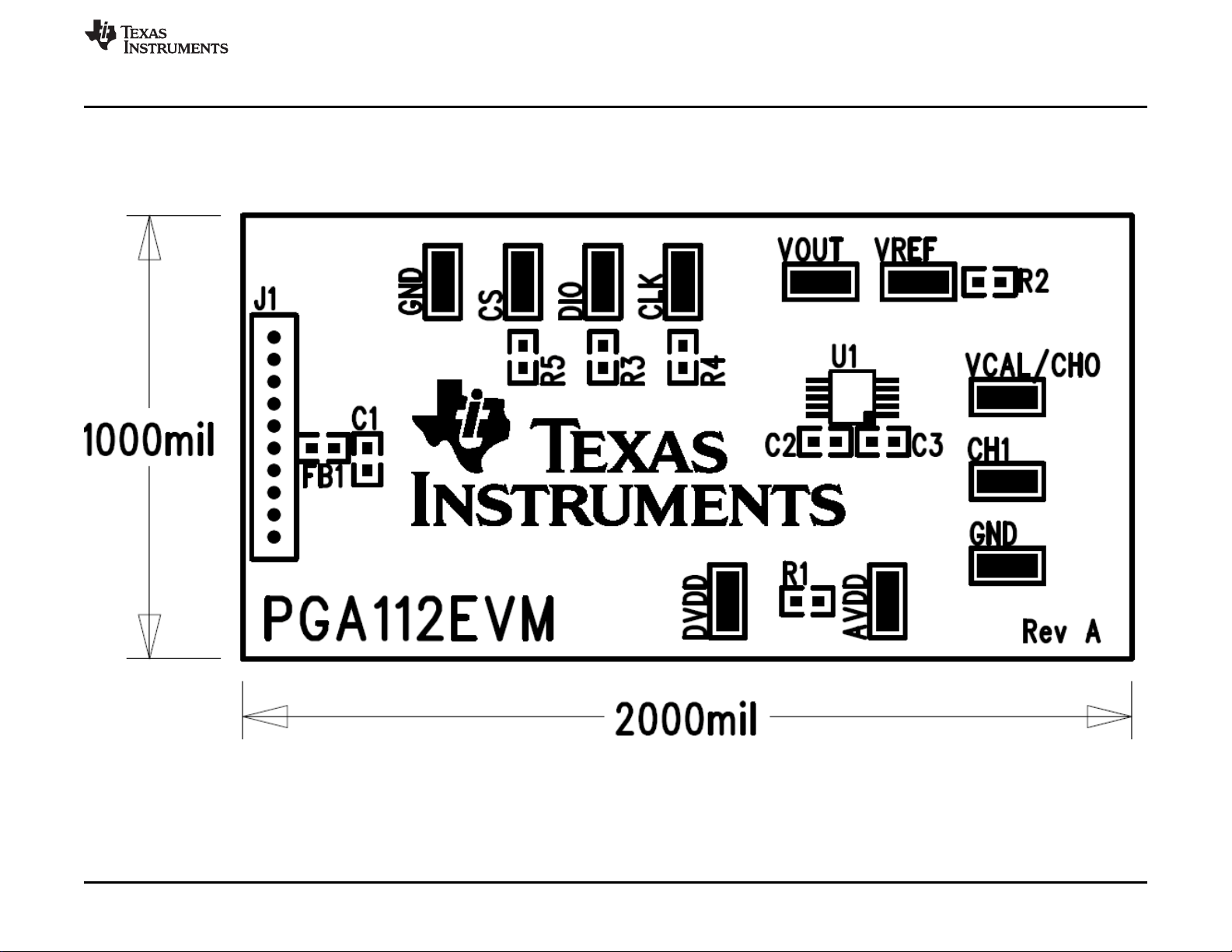
6.3 PCB Layout
Figure 17 shows the layout of the components for the PGA112EVM board. Note that the PGA113EVM layout is identical, except for the device
name.
EVM Documentation
Figure 17. PCB Component Layout
SBOU073A–February 2009–Revised May 2012 PGA112EVM and PGA113EVM User’s Guide
Submit Documentation Feedback
Copyright © 2009–2012, Texas Instruments Incorporated
15
Page 16

EVM Documentation
www.ti.com
EVALUATION BOARD/KIT IMPORTANT NOTICE
Texas Instruments (TI) provides the enclosed product(s) under the following conditions:
This evaluation board/kit is intended for use for ENGINEERING DEVELOPMENT, DEMONSTRATION, OR EVALUATION PURPOSES
ONLY and is not considered by TI to be a finished end-product fit for general consumer use. Persons handling the product(s) must have
electronics training and observe good engineering practice standards. As such, the goods being provided are not intended to be complete
in terms of required design-, marketing-, and/or manufacturing-related protective considerations, including product safety and environmental
measures typically found in end products that incorporate such semiconductor components or circuit boards. This evaluation board/kit does
not fall within the scope of the European Union directives regarding electromagnetic compatibility, restricted substances (RoHS), recycling
(WEEE), FCC, CE or UL, and therefore may not meet the technical requirements of these directives or other related directives.
Should this evaluation board/kit not meet the specifications indicated in the User’s Guide, the board/kit may be returned within 30 days from
the date of delivery for a full refund. THE FOREGOING WARRANTY IS THE EXCLUSIVE WARRANTY MADE BY SELLER TO BUYER
AND IS IN LIEU OF ALL OTHER WARRANTIES, EXPRESSED, IMPLIED, OR STATUTORY, INCLUDING ANY WARRANTY OF
MERCHANTABILITY OR FITNESS FOR ANY PARTICULAR PURPOSE.
The user assumes all responsibility and liability for proper and safe handling of the goods. Further, the user indemnifies TI from all claims
arising from the handling or use of the goods. Due to the open construction of the product, it is the user’s responsibility to take any and all
appropriate precautions with regard to electrostatic discharge.
EXCEPT TO THE EXTENT OF THE INDEMNITY SET FORTH ABOVE, NEITHER PARTY SHALL BE LIABLE TO THE OTHER FOR ANY
INDIRECT, SPECIAL, INCIDENTAL, OR CONSEQUENTIAL DAMAGES.
TI currently deals with a variety of customers for products, and therefore our arrangement with the user is not exclusive.
TI assumes no liability for applications assistance, customer product design, software performance, or infringement of patents or
services described herein.
Please read the User’s Guide and, specifically, the Warnings and Restrictions notice in the User’s Guide prior to handling the product. This
notice contains important safety information about temperatures and voltages. For additional information on TI’s environmental and/or
safety programs, please contact the TI application engineer or visit www.ti.com/esh.
No license is granted under any patent right or other intellectual property right of TI covering or relating to any machine, process, or
combination in which such TI products or services might be or are used.
FCC Warning
This evaluation board/kit is intended for use for ENGINEERING DEVELOPMENT, DEMONSTRATION, OR EVALUATION PURPOSES
ONLY and is not considered by TI to be a finished end-product fit for general consumer use. It generates, uses, and can radiate radio
frequency energy and has not been tested for compliance with the limits of computing devices pursuant to part 15 of FCC rules, which are
designed to provide reasonable protection against radio frequency interference. Operation of this equipment in other environments may
cause interference with radio communications, in which case the user at his own expense will be required to take whatever measures may
be required to correct this interference.
EVM WARNINGS AND RESTRICTIONS
It is important to operate this EVM within the input voltage range of 0V to 5V and the output voltage range of 0 V to 5 V.
Exceeding the specified input range may cause unexpected operation and/or irreversible damage to the EVM. If there are questions
concerning the input range, please contact a TI field representative prior to connecting the input power.
Applying loads outside of the specified output range may result in unintended operation and/or possible permanent damage to the EVM.
Please consult the EVM User's Guide prior to connecting any load to the EVM output. If there is uncertainty as to the load specification,
please contact a TI field representative.
During normal operation, some circuit components may have case temperatures greater than +25°C. The EVM is designed to operate
properly with certain components above +125°C as long as the input and output ranges are maintained. These components include but are
not limited to linear regulators, switching transistors, pass transistors, and current sense resistors. These types of devices can be identified
using the EVM schematic located in the EVM User's Guide. When placing measurement probes near these devices during operation,
please be aware that these devices may be very warm to the touch.
Mailing Address: Texas Instruments, Post Office Box 655303, Dallas, Texas 75265
Copyright © 2009, Texas Instruments Incorporated
16
PGA112EVM and PGA113EVM User’s Guide SBOU073A–February 2009–Revised May 2012
Copyright © 2009–2012, Texas Instruments Incorporated
Submit Documentation Feedback
 Loading...