

Page 1

User's Guide
SBAU108A–January 2005 – Revised February 2005
PCM4201EVM User's Guide
This document provides the information needed to set up and operate the
PCM4201EVM evaluation module (EVM). For a more detailed description of the
PCM4201, please refer to the product datasheet available from the Texas Instruments
web site at www.ti.com. Additional support documents are listed in the section of this
guide entitled Related Documentation from Texas Instruments and Additional
Documentation. Throughout this document, the acronym EVM and the phrase
evaluation module are synonymous with the PCM4201EVM. This user’s guide
includes setup and configuration instructions, information regarding absolute operating
conditions, an electrical schematic, PCB layout drawings, and a bill of materials (BOM)
for the EVM.
Contents
1 Introduction .......................................................................................... 2
2 Getting Started ...................................................................................... 5
3 Hardware Description and Configuration ........................................................ 6
4 Schematic, PCB Layout, and Bill of Materials................................................. 10
List of Figures
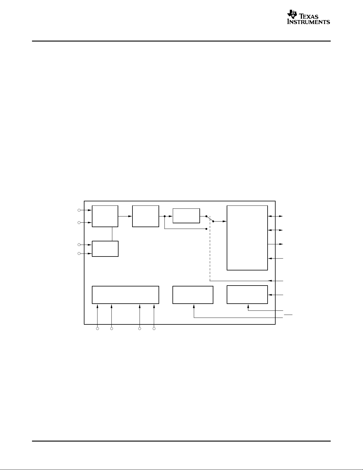
1 PCM4201 Functional Block Diagram ............................................................ 2
2 PCM4201EVM Functional Block Diagram....................................................... 3
3 Transmitter Reset Circuitry ........................................................................ 9
4 PCM4201EVM Schematic ....................................................................... 11
5 Top Side Silkscreen .............................................................................. 12
6 Bottom Side Silkscreen........................................................................... 13
7 Top Layer (Component Side).................................................................... 14
8 Ground Layer ...................................................................................... 15
9 Power Plane Layer................................................................................ 16
10 Bottom Layer (Solder Side) ...................................................................... 17
List of Tables
1 Absolute Operating Conditions ................................................................... 5
2 System Clock Source Selection .................................................................. 7
3 Sampling Mode Selection ......................................................................... 7
4 Digital High-Pass Filter Configuration ........................................................... 7
5 Slave/Master Mode Configuration ............................................................... 8
6 System Clock Rates for Master Mode Operation .............................................. 8
7 System Clock Rates for Slave Mode Operation ............................................... 8
8 Digital Interface Transmitter Configuration ..................................................... 9
9 Transmitter Master Clock Configuration ........................................................ 9
10 PCM4201EVM Bill of Materials.................................................................. 18
PCM4201EVM User's GuideSBAU108A–January 2005–Revised February 2005 1
Page 2
www.ti.com
HPF
Delta−Sigma
Modulator
Decimation
Filter
Voltage
Reference
V
REF
+
V
REF
−
VINR+
VINR
−
Power
V
DD
AGND
Reset
Logic
Clock
Control
Audio
Serial
Port
DGND
V
CC
FSYNC
BCK
DATA
S/M
RATE
SCKI
RST
HPFD
Introduction
1 Introduction
The PCM4201 is a low power, high-performance, single channel audio analog-to-digital (A/D) converter
designed for use in battery-operated or portable professional audio applications, including digital wireless
microphones and digital audio recorders/processors. The PCM4201 features a 24-bit linear PCM data
output, with a data format compatible with digital signal processors and digital audio interface transmitters
(including the DIT4096 and DIT4192 from Texas Instruments).
The PCM4201 includes three sampling modes, supporting sampling rates up to 108kHz. The Normal
Speed Low Power mode supports sampling rates up to 54kHz, and employs 64x oversampling to reduce
overall converter power. The Normal Speed High Performance mode supports sampling rates up to 54kHz
with 128x oversampling, resulting in higher dynamic range than the Low Power mode, at the expense of
increased power dissipation. The Double Speed mode supports sampling frequencies up to 108kHz, and
is provided for those cases where higher sampling rates may be required.
A digital high-pass filter is included for DC removal. Dedicated control pins are included for sampling mode
selection, Slave/Master mode port operation, digital high-pass filter enable/disable, and reset/power-down
functions.
A +5V power supply is required for the analog section of the device, while a +3.3V power supply is
typically utilized for the digital circuitry. The digital supply may operate at voltages as low as +1.8V, with a
corresponding 10mW to 20mW reduction in power dissipation, depending upon the sampling mode
selection. Figure 1 illustrates the functional block diagram for the PCM4201.
1.1 PCM4201EVM Features
The PCM4201EVM provides a convenient platform for evaluating the performance and functions of the
PCM4201 device. The primary EVM features include:
• Simple configuration using an onboard DIP switch
• Differential voltage input supporting 3-pin XLR or balanced TRS connections
• Differential input buffer and filter circuit utilizing the Texas Instruments OPA2134 dual op amp
• Flexible input buffer power supply connection (dual or single supply options) and resistor/capacitor
PCM4201EVM User's Guide2 SBAU108A – January 2005 – Revised February 2005
configuration allow for circuit experimentation and op amp substitution
Figure 1. PCM4201 Functional Block Diagram
Page 3
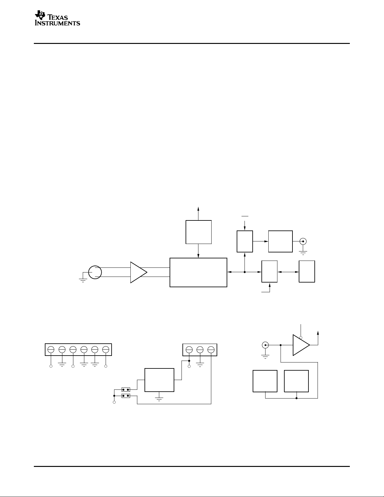
www.ti.com
J1
Analog
Input
Analog
Input Buffer
U1
PCM4201
Switch
SW1
To
DIT Circuitry
and
Clock Enables
X1
22.5792M
J4
EXT CLOCK INPUT
System
Clock
X2
24.576M
S/M
U2
OPA2134
GND
J2
+5VA+15V
−
15V
−
15V
GND
+15V
GND
+5VA
U10
REG1117
+3.3V
J6
+5VD
+5VD
GND
EXT VDD
VDD
JMP4
BUF
S/M
PCM Data
HDR
J3
Audio
Serial Port
BUF
DIT
U7
DIT4096
J5
AES3 Output
• Buffered audio serial port output supports connection to external DSP hardware or audio test
equipment
• An onboard Texas Instruments DIT4096 provides an AES3-encoded digital output suitable for use with
audio test systems or commercial audio equipment, supporting output sampling rates up to 108kHz
• Onboard crystal oscillators, operating at 22.5792MHz and 24.576MHz, support 44.1kHz, 48kHz,
88.2kHz, and 96kHz sampling rates and all three sampling modes of the PCM4201
• An external clock input allows operation at alternative sampling frequencies
As shipped, the PCM4201EVM requires +15V, –15V, and +5V analog power supplies. Options are
provided to operate the analog section from a single power supply by utilizing alternative op amps for the
input buffer circuit. A +5V digital supply is required, with a +3.3V digital supply being derived onboard
using a Texas Instruments REG1117 voltage regulator IC. Connections are provided for an external digital
supply for the PCM4201, allowing digital operation down to +1.8V.
1.2 PCM4201EVM General Description and Functional Block Diagram
The PCM4201EVM provides a complete platform for evaluating the performance and features of the
PCM4201 single channel audio A/D converter. Figure 2 illustrates the functional block diagram for the
evaluation module.
Introduction
Figure 2. PCM4201EVM Functional Block Diagram
PCM4201EVM User's GuideSBAU108A – January 2005 – Revised February 2005 3
Page 4

www.ti.com
Introduction
A differential analog input is supported at connector J1. The analog input supports either a 3-pin male XLR
or balanced TRS input plug. The analog input is buffered and filtered using a low noise input circuit,
utilizing a Texas Instruments' OPA2134 dual audio op amp IC. The output of the buffer circuit is connected
to the differential input of the PCM4201, which is then used to convert the analog signal to a 24-bit linear
PCM representation in the digital domain.
The 24-bit PCM output data is made available at header J3. The audio data can also be routed to the
DIT4096 digital interface transmitter, supporting an AES3-encoded output, which is provided at BNC
connector J5. The buffered header is convenient for interfacing to external development hardware or
digital signal processors, while the AES3-encoded outputs may be connected to audio test systems or
commercial audio equipment.
Power is connected to the board at either terminal block J2 for the analog supplies, or at terminal block J6
for the digital supplies.
Manual reset circuits are provided for both the PCM4201 (U1) and the DIT4096 (U7). The ADC RESET
switch (SW2) is utilized for resetting the A/D converter, while the DIT RESET switch (SW3) is utilized for
resetting the AES3 transmitter.
The system or master clock for the evaluation module may be generated onboard or by an external clock
source. Oscillators X1 and X2 operate at fixed clock frequencies of 22.5792MHz and 24.576MHz,
respectively. The oscillators provide low jitter clock sources for measuring the performance of the
PCM4201 in Master mode operation. Alternatively, an external clock source may be connected at J4 for
Master mode operation, supporting alternative sampling rates. For Slave mode operation, the system
clock is provided from an external source through header J3. Switch SW1 provides configuration control
for the PCM4201, the DIT4096, the onboard oscillators, and the external clock input at connector J4.
1.3 Related Documentation from Texas Instruments
The following documents provide information regarding Texas Instruments integrated circuits used in the
assembly of the PCM4201EVM. The latest revisions of these documents are available from the TI web
site at www.ti.com .
Data Sheet Literature Number
PCM4201 Datasheet SBAS342
DIT4096 Datasheet SBOS225
OPA2134 Datasheet SBOS058
REG1117 Datasheet SBVS001
SN74ALVC245 Datasheet SCES271
SN74LVC1G04 Datasheet SCES214
SN74LVC1G08 Datasheet SCES217
SN74LVC1G125 Datasheet SCES223
1.4 Additional Documentation
The following documents or references provide information regarding selected non-TI components used in
the assembly of the PCM4201EVM. These documents are available from the corresponding manufacturer.
Document/Reference Manufacturer
SM7745H Series CMOS Oscillators Pletronics (http://www.pletronics.com )
PCM4201EVM User's Guide4 SBAU108A – January 2005 – Revised February 2005
Page 5
www.ti.com
2 Getting Started
This section provides information regarding handling, package contents, and absolute operating conditions
for the PCM4201EVM.
2.1 Electrostatic Discharge Warning
Failure to observe proper ESD handling precautions may result in damage
to EVM components.
Many of the components used in the assembly of the PCM4201EVM are susceptible to damage by
electrostatic discharge (ESD). Customers are advised to observe proper ESD handling procedure when
unpacking and handling the PCM4201EVM. All handling should be performed at an approved ESD
workstation or test bench, using a grounded wrist strap. Failure to observe proper handling procedure may
result in damage to the EVM and/or the module components.
2.2 EVM Package Contents
Upon opening the PCM4201EVM package, please check to make sure that these items are included:
• One PCM4201EVM evaluation module
• One printed copy of the PCM4201 product datasheet
• One printed copy of this PCM4201EVM User’s Guide
If any of these items are missing, please contact the TI Product Information Center in your region.
Getting Started
CAUTION
2.3 Absolute Operating Conditions
The user should be aware of the absolute operating conditions for the PCM4201EVM. Table 1
summarizes the critical data points.
Power Supplies
+15V +5.0 +18.0 V
-15V -5.0 -18.0 V
+5VA +4.5 +5.5 V
+5VD +4.5 +5.5 V
EXT VDD +1.8 +3.6 V
Audio Serial Port (J3)
VIH, Input High Voltage 0.7 x V
VIL, Input Low Voltage -0.3 0.3 x V
External Clock Input (J4)
VIH, Input High Voltage 0.7 x V
VIL, Input Low Voltage -0.3 0.3 x V
Analog Inputs (J1)
Input Voltage, Differential 0 18.5 V
CAUTION
Exceeding the absolute operating conditions may result in damage to the
evaluation module and/or the equipment connected to it.
Table 1. Absolute Operating Conditions
Min Max Units
DD
DD
+3.6 V
DD
+3.6 V
DD
V
V
PP
PCM4201EVM User's GuideSBAU108A – January 2005 – Revised February 2005 5
Page 6

www.ti.com
Hardware Description and Configuration
3 Hardware Description and Configuration
This section provides hardware description and configuration information for the PCM4201EVM.
3.1 Power Supply Configuration
The PCM4201EVM requires three analog power supplies and one digital power supply for operation. The
analog supplies are connected at terminal block J2, while the digital supply is connected at terminal block
J6.
Analog supplies include +15V and –15V DC for powering the input buffer circuit, as well as +5.0V DC for
powering the analog section of the PCM4201. All supplies should be rated for at least 500mA of output
current.
The digital supply requires +5.0V DC and should be rated for at least 500mA of output current. The +5.0V
supply is regulated to +3.3V DC by an onboard Texas Instruments REG1117 linear voltage regulator
(U10), which is used to power the digital section of the PCM4201 and the majority of the support logic
circuitry. The core logic and line driver sections of the AES3 transmitter (U7) utilize the +5.0V digital
supply directly.
An optional external VDD power supply is supported at terminal block J6. Jumper JMP4 is utilized to
select either the onboard +3.3V voltage regulator (U10) or an external power source. Shorting pins 1 and
2 together using the supplied jumper block selects the onboard +3.3V voltage regulator. Shorting pins 3
and 4 together will select the external supply (EXT VDD) on terminal block J6. Only one source may be
selected at any time.
The External VDD may be operated as low as +1.8V. However, the DIT4096 transmitter will only operate
at voltages down to +2.0V. Use the audio serial port interface at header J3 when operating VDD at
voltages lower than +2.0V.
3.2 Analog Input
The PCM4201EVM includes a Neutrik combo XLR connector (J1), which accepts either a 3-pin male XLR
or a 1/4-inch TRS phono plug. The analog input can accept up to a 18.5V
signal is then attenuated by a factor of 3.7 by the input buffer circuit, which corresponds to the 5.0V
scale differential input voltage for the PCM4201 analog input.
The input buffer circuit is comprised of an OPA2134 dual audio operational amplifier and associated
passive components. The input buffer provides active attenuation and low-pass filtering for the analog
input signal. The OPA2134 is biased to approximately +2.5V, with the bias voltage being derived from the
+5V analog supply using a voltage divider.
The input buffer circuit may be configured to accept either dual or single supply op amps. Jumper JMP2
allows the –15V supply to be shorted to ground. The +15V may then be adjusted to the appropriate single
supply voltage for the op amp. When using a single supply op amp, it may be necessary to change the
values of the buffer feedback and input resistors in order to adjust the gain or attenuation to match the
maximum input/output voltage swing allowed by the single supply configuration.
3.3 System Clock Configuration
The OSC1 and OSC2 elements of switch SW1 are utilized to select the system clock source for the
PCM4201EVM. Table 2 summarizes the available options. The onboard oscillators support 44.1kHz,
48kHz, 88.2kHz, and 96kHz sampling rates for Master mode audio serial port operation. Alternatively, the
external clock input (J4) may be used to supply the system clock from an external source, supporting
additional sampling rates.
For Slave mode operation, the system clock is input at the SCKI pin of the audio serial port header (J3).
differential input signal. This
PP
full
PP
6 SBAU108A – January 2005 – Revised February 2005PCM4201EVM User's Guide
Page 7
www.ti.com
F
3dB
f
S
48,000
, where fS output sampling rate
OSC2 OSC1 SYSTEM CLOCK SOURCE
LO HI X1, 22.5792MHz
HI LO X2, 24.576MHz
LO LO External Clock from connector J3 or J4
3.4 Sampling Mode Selection
The PCM4201 supports three sampling modes, allowing the user to select the best power/performance
combination for a given application.
The Normal Speed Low Power mode provides the lowest overall power dissipation while supporting
sampling rates up to 54kHz. The modulator oversampling rate is 64f
The Normal Speed High Performance mode provides the best dynamic performance at the expense of
increased power dissipation. Sampling rates up to 54kHz are supported. The modulator oversampling rate
is 128f
Power mode.
The Double Speed mode supports sampling frequencies up to 108kHz with power dissipation just slightly
higher than the Normal Speed High Performance mode. The modulator oversampling rate is 64f
mode.
The sampling mode is selected using the RATE VDD and RATE GND elements of switch SW1. Table 3
shows the settings required for each sampling mode.
Hardware Description and Configuration
Table 2. System Clock Source Selection
for this mode.
S
for this mode, improving the overall dynamic range and THD+N when compared to the Low
S
for this
S
RATE VDD RATE GND SAMPLING MODE
OFF ON Double Speed
ON OFF Normal Speed Low Power
OFF OFF Normal Speed High Performance
3.5 Digital High-Pass Filter
The PCM201 includes a digital high-pass filter, which is utilized to remove the DC component from the
digitized signal. The high-pass filter is located at the output of the digital decimation filter in the overall A/D
signal chain. The –3dB corner frequency of the high-pass filter is set by the following relationship:
The digital high-pass filter may be enabled or disabled using the HPFD element of switch SW1. Table 4
summarizes the HPFD switch settings. There may be a small increase distortion for low frequency inputs
(less than 100Hz) when the high-pass filter is enabled.
HPFD HIGH-PASS FILTER FUNCTION
LO Enabled
Table 3. Sampling Mode Selection
Table 4. Digital High-Pass Filter Configuration
HI Disabled
PCM4201EVM User's GuideSBAU108A – January 2005 – Revised February 2005 7
Page 8

www.ti.com
Hardware Description and Configuration
3.6 Audio Serial Port Interface
The PCM4201EVM audio serial port is accessed at header J3. The port includes the audio bit clock
(BCK), the audio frame synchronization clock (FSYNC), and the serial audio data (DATA). The system
clock (SCKI) is also available at the audio serial port. The audio serial port may be operated in Slave or
Master Mode.
In Slave Mode, the BCK, FSYNC, and SCKI clocks are inputs to the PCM4201EVM, and may be provided
from an external source (DSP, FPGA, etc.) via header J3. The BCK and FSYNC clocks must be
synchronous with one another and the audio data.
In Master Mode, the BCK, FSYNC, and SCKI clocks are outputs, being derived by the PCM4201 using the
on-board crystal oscillators or external clock source applied at connector J4.
The Slave or Master Mode port configuration is programmed using the S/M element of switch SW1.
Table 5 summarizes the available settings.
Table 5. Slave/Master Mode Configuration
S/M AUDIO SERIAL PORT SLAVE/MASTER MODE
LO Master
HI Slave
Slave or Master Mode audio serial port operation also dictates the required rate of the system clock
(SCKI) supported for various sampling modes. A summary of the supported rates is shown in Table 6 and
Table 7 .
3.7 Digital Interface Transmitter
A Texas Instruments DIT4096 digital interface transmitter provides an AES3-encoded output for the
PCM4201EVM. The DIT and DITCLK elements of switch SW1 are utilized to configure the transmitter.
The output of the transmitter is available at connector J5. This output is designed for use with 75 Ω coaxial
cable connections.
The transmitter is enabled using the DIT element of switch SW1. The DIT switch operation is summarized
in Table 8 .
Table 6. System Clock Rates for Master Mode Operation
SCKI RATE SAMPLING MODE WITH MASTER MODE AUDIO SERIAL PORT
512f
S
512f
S
256f
S
Normal Speed Low Power
Normal Speed High Performance
Double Speed
Table 7. System Clock Rates for Slave Mode Operation
SCKI RATE SAMPLING MODE WITH SLAVE MODE AUDIO SERIAL PORT
256f
or 512f
S
256f
S
256f
S
or 512f
S
S
Normal Speed Low Power
Normal Speed High Performance
Double Speed
8 SBAU108A – January 2005 – Revised February 2005PCM4201EVM User's Guide
Page 9

www.ti.com
U9
To RST of U7
From DIT
VDD
SW4
N.O.
U8
Hardware Description and Configuration
Table 8. Digital Interface Transmitter Configuration
DIT DIGITAL INTERFACE TRANSMITTER
LO Enabled
HI Disabled
The audio data format for the transmitters is hardwired for 24-bit Left Justified data format. Only one
channel (Channel A of the AES3 stream) will carry 24-bit linear PCM audio data.
Like the PCM4201, the DIT4096 transmitters must be configured for the proper Master (or System) clock
frequency. The transmitter master clock is driven by the same source as the PCM4201 system clock, as
described in Section 3.3 of this document. The transmitter master clock rate selection must match the
system clock rate selection for the PCM4201. Table 9 summarizes the master clock rate options for the
DIT4096 transmitter using the DITCLK element of switch SW1.
Table 9. Transmitter Master Clock Configuration
DITCLK TRANSMITTER MASTER CLOCK RATE
LO 256f
HI 512f
S
S
3.8 Reset Operations
The PCM4201EVM includes two reset switches, SW2 and SW3. Both are momentary contact, normally
open pushbutton switches. Switch SW2 provides the manual reset for the PCM4201, while switch SW3
provides the manual reset the DIT4096 digital interface transmitter.
The PCM4201 may be reset at any time by momentarily pressing and then releasing switch SW2. This
generates a reset pulse and initiates a reset sequence for the device.
For the transmitter reset function, the output of the reset circuit is connected to the RST pin of the
DIT4096 transmitter. The DIT4096 may be reset only when the DIT switch of SW1 is set LO by
momentarily pressing and then releasing switch SW3. If the DIT switch is set HI, the output of the AND
gate in the reset circuit is forced low, which will force the transmitter into power down mode. The
transmitter reset circuit is shown in Figure 3 .
Figure 3. Transmitter Reset Circuitry
PCM4201EVM User's GuideSBAU108A – January 2005 – Revised February 2005 9
Page 10

www.ti.com
Schematic, PCB Layout, and Bill of Materials
4 Schematic, PCB Layout, and Bill of Materials
This section provides the electrical schematic and physical layout information for the PCM4201EVM. The
bill of materials (BOM) is included as a component reference.
Note:
Board layouts are not to scale. These figures are intended to show how the board is laid
out; they are not intended to be used for manufacturing PCM4201EVM PCBs.
PCM4201EVM User's Guide10 SBAU108A – January 2005 – Revised February 2005
Page 11

www.ti.com
4.1 Schematic
The electrical schematic for the PCM4201EVM is shown in Figure 4. The components shown in the
schematic are listed in Table 10 for reference.
Schematic, PCB Layout, and Bill of Materials
Figure 4. PCM4201EVM Schematic
PCM4201EVM User's GuideSBAU108A–January 2005–Revised February 2005 11
Page 12

www.ti.com
Schematic, PCB Layout, and Bill of Materials
4.2 PCB Layout
The PCB layout is a 4-layer printed circuit board (PCB) with the following layer structure:
• Layer 1: Top (component side)
• Layer 2: Ground plane
• Layer 3: Power
• Layer 4: Bottom (solder side)
Figure 5 through Figure 10 show the top and bottom side silkscreen images, along with top, ground plane,
power, and bottom layers of the PCB.
Figure 5. Top Side Silkscreen
PCM4201EVM User's Guide12 SBAU108A – January 2005 – Revised February 2005
Page 13

www.ti.com
Schematic, PCB Layout, and Bill of Materials
Figure 6. Bottom Side Silkscreen
PCM4201EVM User's GuideSBAU108A – January 2005 – Revised February 2005 13
Page 14

www.ti.com
Schematic, PCB Layout, and Bill of Materials
Figure 7. Top Layer (Component Side)
PCM4201EVM User's Guide14 SBAU108A – January 2005 – Revised February 2005
Page 15

www.ti.com
Schematic, PCB Layout, and Bill of Materials
Figure 8. Ground Layer
PCM4201EVM User's GuideSBAU108A – January 2005 – Revised February 2005 15
Page 16

www.ti.com
Schematic, PCB Layout, and Bill of Materials
Figure 9. Power Plane Layer
PCM4201EVM User's Guide16 SBAU108A – January 2005 – Revised February 2005
Page 17

www.ti.com
Schematic, PCB Layout, and Bill of Materials
Figure 10. Bottom Layer (Solder Side)
PCM4201EVM User's GuideSBAU108A – January 2005 – Revised February 2005 17
Page 18

Schematic, PCB Layout, and Bill of Materials
4.3 Bill of Materials
The Bill of Materials, listing the components use in the assembly of the PCM4201EVM, is shown in
Table 10.
Table 10. PCM4201EVM Bill of Materials
www.ti.com
ITEM VALUE Ref Des BOARD MFR MFR PART NUMBER DESCRIPTION
1 100pF C43, C44 2 TDK C2012C0G1H101J Chip Capacitor, C0G Ceramic,
2 1000pF C45, C46 2 TDK C2012C0G1H102J Chip Capacitor, C0G Ceramic,
3 2700pF C47 1 TDK C2012C0G1H272J Chip Capacitor, C0G Ceramic,
4 N/A C41, C42 N/A N/A N/A Optional Component; Not Installed,
5 0.01µF C37-C40 4 TDK C2012X7R1H103K Chip Capacitor, X7R Ceramic,
6 0.1µF C18-C36 19 TDK C2012X7R1H104K Chip Capacitor, X7R Ceramic,
7 10µF C8-C17 10 Kemet T494C106K025AS Chip Capacitor, Low ESR Tantalum,
8 100µF C1-C7 7 Panasonic EEV-FK1E101XP Capacitor, SMT Aluminum Electrolytic,
9 J1 1 Neutrik NCJ6FI-H Combo Connector, Female XLR and
10 J2 1 Weidmuller 996772 3.5mm PCB Terminal Block, 6 poles
11 J3 1 Samtec TSW-105-07-G-D Terminal Strip, 10-pin (5x2)
12 J4, J5 2 Amp 414305-1 RCA Phono Jack, Black Shell
13 J6 1 Weidmuller 1699680000 3.5mm PCB Terminal Block, 3 poles
14 JMP1, JMP2 2 Samtec TSW-102-07-G-S Terminal Strip, 2-pin (2x1)
15 JMP4 1 Samtec TSW-102-07-G-D Terminal Strip, 4-pin (2x2)
16 0 R12, R13 2 Panasonic ERJ-6GEY0R00V Chip Resistor, 0W, Shunt, Size = 0805
17 40.2 R10, R11 2 Panasonic ERJ-6ENF40R2V Chip Resistor, Thick Film, 1% Toler-
18 121 R14 1 Panasonic ERJ-6ENF1210V Chip Resistor, Thick Film, 1% Toler-
19 150 R5 1 Panasonic ERJ-6ENF1500V Chip Resistor, Thick Film, 1% Toler-
20 270 R6, R7 2 Panasonic ERA-6YEB271V Chip Resistor, Metal Film, 0.1% Toler-
21 1K R8, R9 2 Panasonic ERA-6YEB102V Chip Resistor, Metal Film, 0.1% Toler-
22 10K R1-R4 4 Panasonic ERJ-6ENF1002V Chip Resistor, Thick Film, 1% Toler-
23 10K RN1 1 CTS 742C163103J Thick Film Chip Resistor Array, 10kW,
24 100 RN2, RN2, 3 CTS 742C083101J Thick Film Chip Resistor Array, 100W,
RN4 16-Terminal, 8 Resistors, Isolated
25 SW1 1 ITT Industries/ TDA08H0SK1 DIP Switch, 8 Element, Half-Pitch,
26 SW2, SW3 2 Omron B3S-1000 Momentary Tact Switch, SMT without
27 U1 1 Texas PCM4201PW Single Channel 24-Bit Audio
QTY PER
100pF ±5%, 50WV, Size = 0805
1000pF ±5%, 50WV, Size = 0805
2700pF ±5%, 50WV, Size = 0805
Size = 0805
0.01µF ±10%, 50WV, Size = 0805
0.1µF ±10%, 50WV, Size = 0805
10µF ±10%, 25WV, Size = C
100µF ±20%, 25WV
TRS, Vertical PC Mount
ance, 40.2W, 1/10W, Size = 0805
ance, 121W, 1/10W, Size = 0805
ance, 150W, 1/10W, Size = 0805
ance, 270W, 1/10W, Size = 0805
ance, 1kW, 1/10W, Size = 0805
ance, 10kW, 1/10W, Size = 0805
16-Terminal, 8 Resistors, Isolated
C&K Surface-Mount, Tape Sealed
Ground Terminal
Instruments A/D Converter
PCM4201EVM User's Guide18 SBAU108A– January 2005 – Revised February 2005
Page 19

www.ti.com
Schematic, PCB Layout, and Bill of Materials
Table 10. PCM4201EVM Bill of Materials (continued)
28 U2 1 Texas OPA2134UA Dual Audio Op Amp
29 U3 N/A N/A N/A Component Removed,
30 U4, U6 2 Texas SN74ALVC245PW Octal Bus Transceiver w/ Tri-State
31 U5 1 Texas SN74LVC1G125DBV Single Non-Inverting Buffer w/
32 U7 1 Texas DIT4096IPW 96kHz Digital Audio Transmitter
33 U8 1 Texas SN74LVC1G04PW Single Inverter
34 U9 1 Texas SN74LVC1G08DBV Single 2-Input Positive AND Gate
35 U10 1 Texas REG1117-3.3 Linear Voltage Regulator, +3.3V
36 X1 1 Pletronics SM7745HSV-22.5792M +3.3V Surface Mount Clock Oscillator
37 X2 1 Pletronics SM7745HSV-24.576M +3.3V Surface Mount Clock Oscillator
38 2 Samtec SNT-100-BK-G-H Shorting Blocks
39 4 3M Bumpon SJ-5003 Self-Adhesive Rubber Feet
Instruments
Reference Maintained
Instruments Outputs
Instruments Tri-State Output
Instruments
Instruments
Instruments
Instruments
CMOS Output with Active High Enable
22.5792MHz ±50ppm
CMOS Output with Active High Enable
24.576MHz ±50ppm
SBAU108A–January 2005–Revised February 2005 PCM4201EVM User's Guide 19
Page 20

FCC Warnings
This equipment is intended for use in a laboratory test environment only. It generates, uses, and can radiate radio frequency
energy and has not been tested for compliance with the limits of computing devices pursuant to subpart J of part 15 of FCC rules,
which are designed to provide reasonable protection against radio frequency interference. Operation of this equipment in other
environments may cause interference with radio communications, in which case the user at his own expense will be required to
take whatever measures may be required to correct this interference.
EVM IMPORTANT NOTICE
Texas Instruments (TI) provides the enclosed product(s) under the following conditions:
This evaluation kit being sold by TI is intended for use for ENGINEERING DEVELOPMENT OR EVALUATION PURPOSES ONLY
and is not considered by TI to be fit for commercial use. As such, the goods being provided may not be complete in terms of
required design-, marketing-, and/or manufacturing-related protective considerations, including product safety measures typically
found in the end product incorporating the goods. As a prototype, this product does not fall within the scope of the European Union
directive on electromagnetic compatibility and therefore may not meet the technical requirements of the directive.
Should this evaluation kit not meet the specifications indicated in the EVM User's Guide, the kit may be returned within 30 days
from the date of delivery for a full refund. THE FOREGOING WARRANTY IS THE EXCLUSIVE WARRANTY MADE BY SELLER
TO BUYER AND IS IN LIEU OF ALL OTHER WARRANTIES, EXPRESSED, IMPLIED, OR STATUTORY, INCLUDING ANY
WARRANTY OF MERCHANTABILITY OR FITNESS FOR ANY PARTICULAR PURPOSE.
The user assumes all responsibility and liability for proper and safe handling of the goods. Further, the user indemnifies TI from all
claims arising from the handling or use of the goods. Please be aware that the products received may not be regulatory compliant
or agency certified (FCC, UL, CE, etc.). Due to the open construction of the product, it is the user's responsibility to take any and all
appropriate precautions with regard to electrostatic discharge.
EXCEPT TO THE EXTENT OF THE INDEMNITY SET FORTH ABOVE, NEITHER PARTY SHALL BE Liable to the other FOR
ANY INDIRECT, SPECIAL, INCIDENTAL, OR CONSEQUENTIAL DAMAGES.
TI currently deals with a variety of customers for products, and therefore our arrangement with the user is not exclusive.
TI assumes no liability for applications assistance, customer product design, software performance, or infringement of
patents or services described herein.
Please read the EVM User's Guide and, specifically, the EVM Warnings and Restrictions notice in the EVM User's Guide prior to
handling the product. This notice contains important safety information about temperatures and voltages. For further safety
concerns, please contact the TI application engineer.
Persons handling the product must have electronics training and observe good laboratory practice standards.
No license is granted under any patent right or other intellectual property right of TI covering or relating to any machine, process, or
combination in which such TI products or services might be or are used.
EVM WARNINGS AND RESTRICTIONS
It is important to operate this EVM with the operating conditions specified within Table 1 of this document.
Exceeding the specified input range may cause unexpected operation and/or irreversible damage to the EVM. If there are
questions concerning the input range, please contact a TI field representative prior to connecting the input power.
Applying loads outside of the specified output range may result in unintended operation and/or possible permanent damage to the
EVM. Please consult the EVM User's Guide prior to connecting any load to the EVM output. If there is uncertainty as to the load
specification, please contact a TI field representative.
During normal operation, some circuit components may have case temperatures greater than 37 ° C. The EVM is designed to
operate properly with certain components above 60 ° C as long as the input and output ranges are maintained. These components
include but are not limited to linear regulators, switching transistors, pass transistors, and current sense resistors. These types of
devices can be identified using the EVM schematic located in the EVM User's Guide. When placing measurement probes near
these devices during operation, please be aware that these devices may be very warm to the touch.
Mailing Address: Texas Instruments, Post Office Box 655303, Dallas, Texas 75265
Copyright © 2005, Texas Instruments Incorporated
Page 21

IMPORTANT NOTICE
Texas Instruments Incorporated and its subsidiaries (TI) reserve the right to make corrections, modifications, enhancements,
improvements, and other changes to its products and services at any time and to discontinue any product or service without notice.
Customers should obtain the latest relevant information before placing orders and should verify that such information is current and
complete. All products are sold subject to TI’s terms and conditions of sale supplied at the time of order acknowledgment.
TI warrants performance of its hardware products to the specifications applicable at the time of sale in accordance with TI’s
standard warranty. Testing and other quality control techniques are used to the extent TI deems necessary to support this
warranty. Except where mandated by government requirements, testing of all parameters of each product is not necessarily
performed.
TI assumes no liability for applications assistance or customer product design. Customers are responsible for their products and
applications using TI components. To minimize the risks associated with customer products and applications, customers should
provide adequate design and operating safeguards.
TI does not warrant or represent that any license, either express or implied, is granted under any TI patent right, copyright, mask
work right, or other TI intellectual property right relating to any combination, machine, or process in which TI products or services
are used. Information published by TI regarding third-party products or services does not constitute a license from TI to use such
products or services or a warranty or endorsement thereof. Use of such information may require a license from a third party under
the patents or other intellectual property of the third party, or a license from TI under the patents or other intellectual property of TI.
Reproduction of information in TI data books or data sheets is permissible only if reproduction is without alteration and is
accompanied by all associated warranties, conditions, limitations, and notices. Reproduction of this information with alteration is an
unfair and deceptive business practice. TI is not responsible or liable for such altered documentation.
Resale of TI products or services with statements different from or beyond the parameters stated by TI for that product or service
voids all express and any implied warranties for the associated TI product or service and is an unfair and deceptive business
practice. TI is not responsible or liable for any such statements.
TI products are not authorized for use in safety-critical applications (such as life support) where a failure of the TI product would
reasonably be expected to cause severe personal injury or death, unless officers of the parties have executed an agreement
specifically governing such use. Buyers represent that they have all necessary expertise in the safety and regulatory ramifications
of their applications, and acknowledge and agree that they are solely responsible for all legal, regulatory and safety-related
requirements concerning their products and any use of TI products in such safety-critical applications, notwithstanding any
applications-related information or support that may be provided by TI. Further, Buyers must fully indemnify TI and its
representatives against any damages arising out of the use of TI products in such safety-critical applications.
TI products are neither designed nor intended for use in military/aerospace applications or environments unless the TI products are
specifically designated by TI as military-grade or "enhanced plastic." Only products designated by TI as military-grade meet military
specifications. Buyers acknowledge and agree that any such use of TI products which TI has not designated as military-grade is
solely at the Buyer's risk, and that they are solely responsible for compliance with all legal and regulatory requirements in
connection with such use.
TI products are neither designed nor intended for use in automotive applications or environments unless the specific TI products
are designated by TI as compliant with ISO/TS 16949 requirements. Buyers acknowledge and agree that, if they use any
non-designated products in automotive applications, TI will not be responsible for any failure to meet such requirements.
Following are URLs where you can obtain information on other Texas Instruments products and application solutions:
Products Applications
Amplifiers amplifier.ti.com Audio www.ti.com/audio
Data Converters dataconverter.ti.com Automotive www.ti.com/automotive
DSP dsp.ti.com Broadband www.ti.com/broadband
Interface interface.ti.com Digital Control www.ti.com/digitalcontrol
Logic logic.ti.com Military www.ti.com/military
Power Mgmt power.ti.com Optical Networking www.ti.com/opticalnetwork
Microcontrollers microcontroller.ti.com Security www.ti.com/security
RFID www.ti-rfid.com Telephony www.ti.com/telephony
Low Power www.ti.com/lpw Video & Imaging www.ti.com/video
Wireless
Wireless www.ti.com/wireless
Mailing Address: Texas Instruments, Post Office Box 655303, Dallas, Texas 75265
Copyright © 2007, Texas Instruments Incorporated
Page 22

Mouser Electronics
Authorized Distributor
Click to View Pricing, Inventory, Delivery & Lifecycle Information:
Texas Instruments:
PCM4201EVM
 Loading...