

Page 1

PCM3070 Application Reference Guide
Reference Guide
Literature Number: SLAU332
March 2011
Page 2

Chapter 1
SLAU332–March 2011
PCM3070 Overview
• Chapter 1: Device Overview
• Chapter 2: PCM3070 Application
• Chapter 3: Device Initialization
• Chapter 4: Example Setups
• Chapter 5: Register Map and Descriptions
space
Features Applications
• Stereo Audio DAC with 100dB SNR • Soundbar
• Stereo Audio ADC with 93dB SNR • Flat Panel Television
• Extensive Signal Processing Options • MP3 Docking stations
• Embedded miniDSP • Cell Phone Docking Stations
• Six Single-Ended or 3 Fully-Differential Analog • Other Stereo or 2.1 Home Audio systems
Inputs
• Stereo Headphone Outputs programmable inputs and outputs,
• Stereo Line Outputs
• Very Low-Noise PGA
• Analog Bypass Mode
• Programmable PLL
• Integrated LDO
• 5mm x 5mm 32-pin QFN Package
The PCM3070 is a flexible stereo audio codec with
fully-programmable miniDSP, fixed predefined and
parameterizable signal processing blocks,
integrated PLL, integrated LDOs and flexible digital
interfaces.
2
PCM3070 Overview SLAU332–March 2011
© 2011, TexasInstruments Incorporated
Submit Documentation Feedback
Page 3
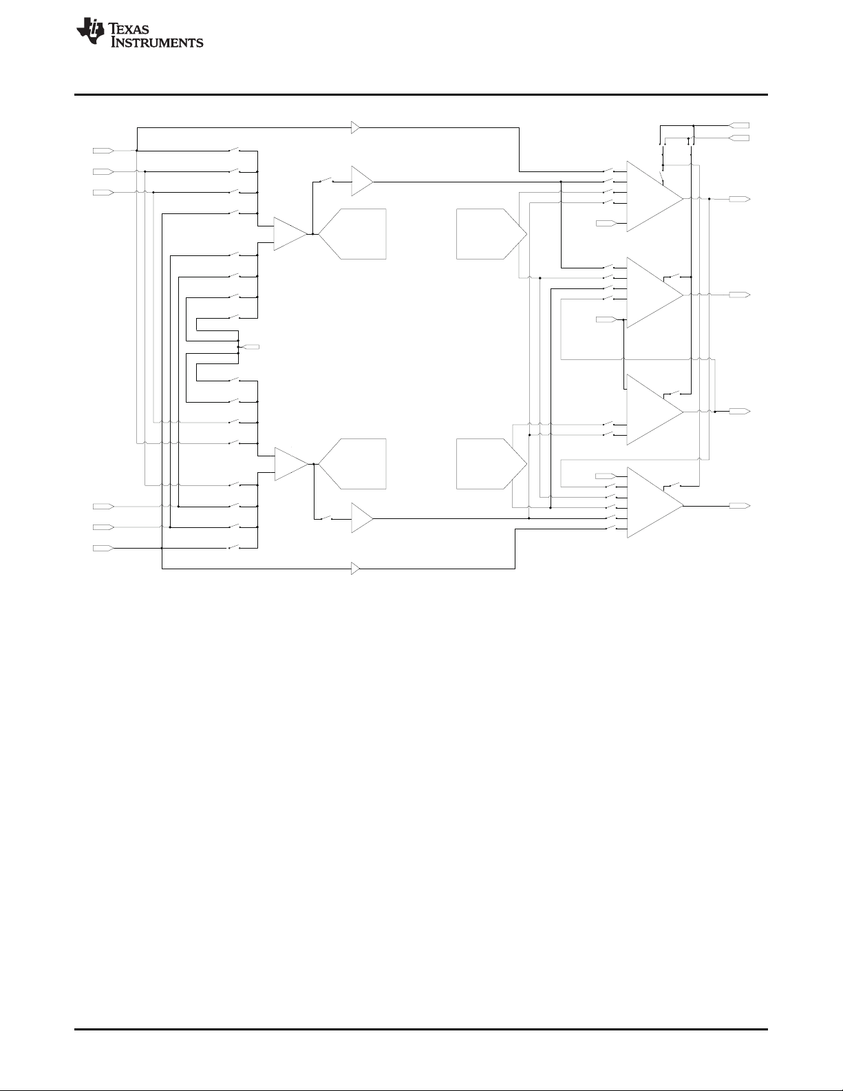
SPI_Select
IN1_R
IN2_R
IN3_R
IN3_L
IN2_L
IN1_L
SCL/SSZ
Left
ADC
DRC
t
pl
Left
DAC
AGC
+
+
+
+
ADC
Signal
Proc.
DAC
Signal
Proc.
Right
ADC
DRC
t
pr
Right
DAC
AGC
ADC
Signal
Proc.
DAC
Signal
Proc.
+
+
+
+
Vol. Ctrl
Vol. Ctrl
Data
Interface
Gain Adj.
Gain Adj.
0…
+47.5 dB
0.5 dB steps
0…+47.5 dB
0.5 dB
steps
-6...+29dB
1dB steps
-6...+29dB
1dB steps
-6...+29dB
1dB steps
-6...+29dB
1dB steps
SPI / I2C
Control Block
Pin Muxing/ Clock Routing
Secondary
I2S IF
Primary
I2S Interface
Interrupt
Ctrl
ALDO
DLDO
PLL
Ref
Ref
LDO Select
Supplies
LDO in
HPVdd
DVdd
AVdd
IOVdd
AVss
DVss
IOVss
SDA/MOSI
MISO
SCLK
MCLK
GPIO
DOUT
DIN
BCLK
WCLK
miniDSP miniDSP
HPL
LOL
HPR
LOR
Reset
-30...0 dB
-30...0 dB
-72...0dB
-72...0dB
´ ´
´´
www.ti.com
1.1 Description
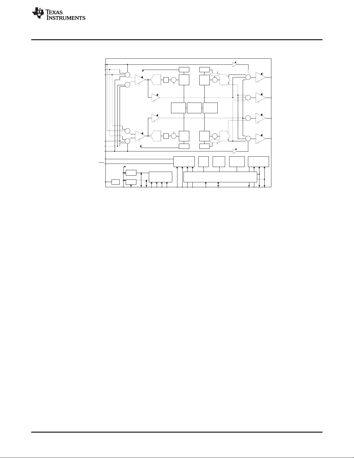
Description
Figure 1-1. Simplified Block Diagram
The PCM3070 features two fully-programmable miniDSP cores that support application-specific algorithms
in the record and/or the playback path of the device. The miniDSP cores are fully software controlled.
Target algorithms, like speaker EQ, Crossovers, Dynamic Range Controls, Intelligent volume controls and
other post-processing algorithms are loaded into the device after power-up.
Extensive register-based control of input/output channel configuration, gains, effects, pin-multiplexing and
clocks is included, allowing the device to be precisely targeted to its application.
The record path of the PCM3070 covers operations from 8kHz mono to 192kHz stereo recording, and
contains programmable input channel configurations covering single-ended and differential setups, as well
as floating or mixed input signals.
The playback path offers signal-processing blocks for filtering and effects, and supports flexible mixing of
DAC and analog input signals as well as programmable volume controls. The playback path contains two
high-power output drivers as well as two fully-differential outputs. The high-power outputs can be
configured in multiple ways, including stereo and mono BTL.
The voltage supply range for the PCM3070 for analog is 1.5V–1.95V, and for digital it is 1.26V–1.95V. To
ease system-level design, LDOs are integrated to generate the appropriate analog or digital supply from
input voltages ranging from 1.8V to 3.6V. Digital I/O voltages are supported in the range of 1.5V–3.6V.
The required internal clock of the PCM3070 can be derived from multiple sources, including the MCLK pin,
the BCLK pin, the GPIO pin or the output of the internal PLL, where the input to the PLL again can be
derived from the MCLK pin, the BCLK or GPIO pins. The PLL is highly programmable and can accept
available input clocks in the range of 512kHz to 50MHz.
The device is available in the 5mm × 5mm, 32-pin QFN package.
SLAU332–March 2011 PCM3070 Overview
Submit Documentation Feedback
© 2011, TexasInstruments Incorporated
3
Page 4
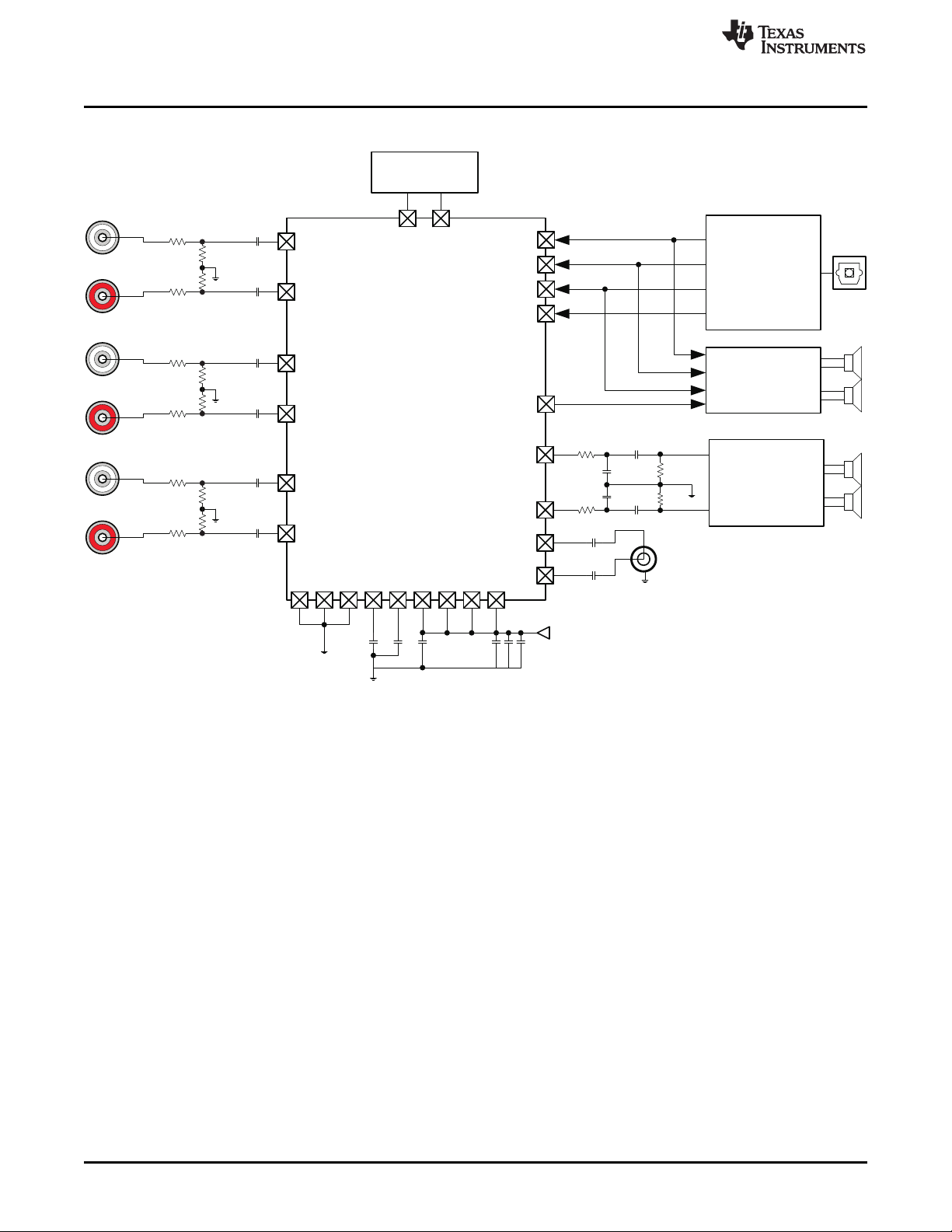
PCM3070
SCL SDA
IN1_L
IN1_R
IN2_L
IN2_R
IN3_L
IN3_R
MCLK
BCLK
WCLK
DIN
DOUT
DIR9001
TAS57xx
LOL
LOR
HPL
HPR
100W
1 Fm
1KW
0.047 Fm
0.047 Fm
TPA3123
LDOIN
LDO_SELECT
IOVDD
IOVSS
DVSS
AVSS
REF
DVDD
AVDD
3V3
47 Fm
MSP430
Headphone
Output
47 Fm
1 Fm
100W
1KW
7.5KW
2.49KW
0.47 Fm
0.47 Fm
2.49KW
7.5KW
7.5KW
2.49KW
0.47 Fm
0.47 Fm
2.49KW
7.5KW
7.5KW
2.49KW
0.47 Fm
0.47 Fm
2.49KW
7.5KW
10 Fm
10 Fm
10 Fm
10 Fm
0.1 Fm
1 Fm
Typical Circuit Configuration
1.2 Typical Circuit Configuration
www.ti.com
Figure 1-2. Typical Circuit Configuration
4
PCM3070 Overview SLAU332–March 2011
© 2011, TexasInstruments Incorporated
Submit Documentation Feedback
Page 5
2.1 Terminal Descriptions
2.1.1 Digital Pins
Only a small number of digital pins are dedicated to a single function; whenever possible, the digital pins
have a default function, and also can be reprogrammed to cover alternative functions for various
applications.
The fixed-function pins are Reset and the SPI_Select pin, which are HW control pins. Depending on the
state of SPI_Select, the two control-bus pins SCL/SS and SDA/MOSI are configured for either I2C or SPI
protocol.
Other digital IO pins can be configured for various functions via register control. An overview of available
functionality is given in Section 2.1.3.
2.1.2 Analog Pins
Chapter 2
SLAU332–March 2011
PCM3070 Application
Analog functions can also be configured to a large degree. Analog blocks are powered down by default.
The blocks can be powered up with fine granularity according to the application needs.
2.1.3 Multifunction Pins
Table 2-1 shows the possible allocation of pins for specific functions. The PLL input, for example, can be
programmed to be any of 4 pins (MCLK, BCLK, DIN, GPIO).
Pin Function MCLK BCLK WCLK DIN DOUT MFP3/ MFP4/ GPIO
A PLL Input S
B Codec Clock Input S
C I2S BCLK input S
D I2S BCLK output E
E I2S WCLK input E, D
F I2S WCLK output E
G I2S ADC word clock input E E
H I2S ADC WCLK out E E
I I2S DIN E, D
J I2S DOUT E, D
K General Purpose Output I E
K General Purpose Output II E
Table 2-1. Multifunction Pin Assignments
1 2 3 4 5 6 7 8
MFP1 MFP2 SCLK MISO MFP5
(1)
(1),D(4)
(2)
S
(2)
S
(2)
,D
(5)
E S
(3)
(3)
S
(1)S(1)
: The MCLK pin can be used to drive the PLL and Codec Clock inputs simultaneously
(2)S(2)
: The BCLK pin can be used to drive the PLL and Codec Clock and audio interface bit clock inputs simultaneously
(3)S(3)
: The GPIO/MFP5 pin can be used to drive the PLL and Codec Clock inputs simultaneously
(4)
D: Default Function
(5)
E: The pin is exclusively used for this function, no other function can be implemented with the same pin (e.g. if GPIO/MFP5 has
been allocated for General Purpose Output, it cannot be used as the INT1 output at the same time)
SLAU332–March 2011 PCM3070 Application
Submit Documentation Feedback
© 2011, TexasInstruments Incorporated
5
Page 6
Terminal Descriptions
Pin Function MCLK BCLK WCLK DIN DOUT MFP3/ MFP4/ GPIO
K General Purpose Output III E
L General Purpose Input I E
L General Purpose Input II E
L General Purpose Input III E
M INT1 output E E E
N INT2 output E E E
Q Secondary I2S BCLK input E E
R Secondary I2S WCLK in E E
S Secondary I2S DIN E E
T Secondary I2S DOUT E
U Secondary I2S BCLK OUT E E E
V Secondary I2S WCLK OUT E E E
W Reserved
X Aux Clock Output E E E
www.ti.com
Table 2-1. Multifunction Pin Assignments (continued)
1 2 3 4 5 6 7 8
MFP1 MFP2 SCLK MISO MFP5
6
PCM3070 Application SLAU332–March 2011
© 2011, TexasInstruments Incorporated
Submit Documentation Feedback
Page 7
www.ti.com
2.1.4 Register Settings for Multifunction Pins
To configure the settings seen in Table 2-1, please see the letter/number combination in Table 2-2 for the
appropriate registers to modify.
Please be aware that more settings may be necessary to obtain a full interface definition matching the
application requirement (e.g. register Page 0 / Register 25 to 33).
Table 2-2. Multifunction Pin Register Configuration
Description Required Register Setting Description
A1 PLL Input on MCLK M5
A2 PLL Input on BCLK M7
A4 PLL Input on DIN/MFP1 M8
A8 PLL Input on GPIO/MFP5 N5 INT2 output DOUT/MFP2
Codec Clock Input on Page 0 / Register 4, Bits INT2 output on Page 0 / Register 55, Bits
B1 N7
MCLK D1-D0=00 MISO/MFP4 D4-D1=0101
Codec Clock Input on Page 0 / Register 4, Bits INT2 output on Page 0 / Register 52, Bits
B2 N8
BCLK D1-D0=01 GPIO/MFP5 D5-D2=0110
Codec Clock Input on D5-D2=0001 Secondary I2S BCLK input D2-D1=01
B8 Q6
GPIO/MPF5 Page 0 / Register 4, Bits on SCLK/MFP3 Page 0 / Register 31, Bits
C2 I2S BCLK input on BCLK Q8
D2 I2S BCLK output on BCLK R6
E3 I2S WCLK input on WCLK R8
F3 I2S WCLK output WCLK S6
I2S ADC word clock input D2-D1=01 Secondary I2S DIN on D5-D2=0001
G6 S8
on SCLK/MFP3 Page 0 / Register 31, Bits GPIO/MFP5 Page 0 / Register 31, Bit
I2S ADC word clock input D5-D2=0001 Secondary I2S DOUT on Page 0 / Register 55, Bits
G8 T7
on GPIO/MFP5 Page 0 / Register 31, Bits MISO/MFP4 D4-D1=1000
Page 0 / Register 4, Bits INT1 output on Page 0 / Register 53, Bits
D3-D2=00 DOUT/MFP2 D3-D1=100
Page 0 / Register 4, Bits INT1 output on Page 0 / Register 55, Bits
D3-D2=01 MISO/MFP4 D4-D1=0100
Page 0 / Register 54, Bits
D2-D1=01 INT1 output on Page 0 / Register 52, Bits
Page 0 / Register 4, Bits GPIO/MFP5 D5-D2=0101
D3-D2=11
Page 0 / Register 52, Bits
D5-D2=0001 Page 0 / Register 53,Bits
Page 0 / Register 4, Bits D3-D1=101
D3-D2=10
Page 0 / Register 52, Bits Page 0 / Register 56, Bits
D1-D0=10 D6-D5=01
Page 0 / Register 27, Bit Secondary I2S BCLK input D5-D2=0001
D3=0 on GPIO/MFP5 Page 0 / Register 31, Bits
Page 0 / Register 27, Bit Secondary I2S WCLK in on D2-D1=01
D3=1 SCLK/MFP3 Page 0 / Register 31, Bits
Page 0 / Register 27, Bit Secondary I2S WCLK in on D5-D2=0001
D2=0 GPIO/MFP50 Page 0 / Register 31, Bits
Page 0 / Register 27, Bit Secondary I2S DIN on D2-D1=01
D2=1 SCLK/MFP3 Page 0 / Register 31, Bit
Page 0 / Register 56, Bits Page 0 / Register 52, Bits
D2-D1=01 D0=0
Page 0 / Register 52, Bits
D2-D1=00
Terminal Descriptions
Required Register
Setting
Page 0 / Register 52, Bits
D6-D5=00
Page 0 / Register 56, Bits
D4-D3=01
Page 0 / Register 52, Bits
D4-D3=0
Page 0 / Register 56, Bits
D0=1
SLAU332–March 2011 PCM3070 Application
Submit Documentation Feedback
© 2011, TexasInstruments Incorporated
7
Page 8
Analog Audio I/O
H7 U5
H8 U7
I4 I2S DIN on DIN/MFP1 U8
J5 V5
K5 V7
K7 V8
K8 W0 Reserved Reserved
L4 X5
L6 X7
L8 X8
www.ti.com
Table 2-2. Multifunction Pin Register Configuration (continued)
Description Required Register Setting Description
I2S ADC WCLK out on Page 0 / Register 55, Bits Secondary I2S BCLK OUT Page 0 / Register 53, Bits
MISO/MFP4 D4-D1=0110 on DOUT/MFP2 D3-D1=110
I2S ADC WCLK out on Page 0 / Register 52, Bits Secondary I2S BCLK OUT Page 0 / Register 55, Bits
GPIO/MFP5 D5-D2=0111 on MISO/MFP4 D4-D1=1001
Page 0 / Register 54, Bits Secondary I2S BCLK OUT Page 0 / Register 52, Bits
D2-D1=01 on GPIO/MFP5 D5-D2=1000
I2S DOUT on Page 0 / Register 53, Bits Secondary I2S WCLK OUT Page 0 / Register 53, Bits
DOUT/MFP2 D3-D1=001 on SCLK/MFP3 D3-D1=111
General Purpose Out I on Page 0 / Register 53, Bits Secondary I2S WCLK OUT Page 0 / Register 55, Bits
DOUT/MFP2 D3-D1=010 on MISO/MFP4 D4-D1=1010
General Purpose Out II Page 0 / Register 55, Bits Secondary I2S WCLK OUT Page 0 / Register 52, Bits
on MISO/MFP4 D4-D1=0010 on GPIO/MFP5 D5-D2=1001
General Purpose Out III Page 0 / Register 52, Bits
on GPIO/MFP5 D5-D2=0011
General Purpose In I on Page 0 / Register 54, Bits Aux Clock Output on Page 0 / Register 53, Bits
DIN/MFP1 D2-D1=10 DOUT/MFP2 D3-D1=011
General Purpose In II on Page 0 / Register 56, Bits Aux Clock Output on Page 0 / Register 55, Bits
SCLK/MFP3 D2-D1=10 MISO/MFP4 D4-D1=0011
General Purpose In III on Page 0 / Register 52, Bits Aux Clock Output on Page 0 / Register 52, Bits
GPIO/MFP5 D5-D2=0010 GPIO/MFP5 D5-D2=0100
Required Register
Setting
2.2 Analog Audio I/O
The analog I/O path of the PCM3070 features a large set of options for signal conditioning as well as
signal routing:
• 6 analog inputs which can be mixed and/or multiplexed in single-ended and/or differential configuration
• 2 programmable gain amplifiers (PGA) with a range of 0 to +47.5dB
• 2 mixer amplifiers for analog bypass
• 2 low power analog bypass channels
• Mute function
• Automatic gain control (AGC)
• Channel-to-channel phase adjustment
• Fast charge of ac-coupling capacitors
• Anti thump
2.2.1 Analog Bypass
The PCM3070 offers two analog-bypass modes. In either of the modes, an analog input signal can be
routed from an analog input pin to an amplifier driving an analog output pin. Neither the ADC nor the DAC
resources are required for such operation.
In analog low-power bypass mode, line-level signals can be routed directly from the analog inputs INL to
the left headphone amplifier (HPL) and INR to HPR.
2.2.2 ADC Bypass Using Mixer Amplifiers
In addition to the analog bypass mode, there is a bypass mode that uses the programmable gain
amplifiers of the input stage in conjunction with a mixer amplifier. With this mode, low-level signals can be
amplified and routed to the line or headphone outputs, fully bypassing the ADC and DAC.
To enable this mode, the mixer amplifiers are powered on via software command.
8
PCM3070 Application SLAU332–March 2011
© 2011, TexasInstruments Incorporated
Submit Documentation Feedback
Page 9
-
+
CM
LADC
IN3_R
IN2_R
IN1_R
HPL
CM HP
MAR
LDAC
MAL
IN1L
IN1_L
IN2_L
IN3_L
LOL
MAL
HPR
CM HP
MAR
RDAC
HPL
IN1R
LOR
MAR
RDAC
LDAC
Left ADC LeftDAC
RightDAC
IN1_R
IN2_R
IN3_R
IN1_L
IN3_L
IN2_L
LeftChannel,InputOptions:
SingleEnded: IN1_L orIN2_L orIN3_L orIN1_R
Differential: IN2_L and IN2_Ror
IN3_L and IN3_R
RightChannel, InputOptions:
SingleEnded: IN1_RorIN2_RorIN3_RorIN2_L
Differential: IN1_Rand IN1_L or
IN3_Rand IN3_L
VolCtrl 0… -72dB
Headphone
Amplifier
-6dB … + 29 dB
CMLO
LineOut
Amplifier
-6dB … + 29 dB
RDAC
LineOut
Amplifier
-6dB … + 29 dB
LDAC
LADCLeft ADC
MixerAmp
0..-30dB
LDOIN
AVDD
LOR
1,10,6
CM2L
CM1L
CM1R
CM2R
Headphone
Amplifier
-6dB … + 29 dB
MicPGA
0...47.5 dB
-
+
MicPGA
0...47.5 dB
N
P
P
N
P
N
N
P
VolCtrl 0… -72dB
MixerAmp
0..-30dB
www.ti.com
Analog Audio I/O
Figure 2-1. Analog Routing Diagram
In analog low-power bypass mode, line-level signals can be routed directly from the analog inputs IN1L to
the left headphone amplifier (HPL) and IN1R to HPR. This is configured on Page 1/ Register 12, Bit D2 for
the left channel and Page 1 / Register 13, Bit D2 for the right channel.
To use the mixer amplifiers, power them on via Page / Register 9, Bits D1-D0.
2.2.3 Headphone Output
The stereo headphone drivers on pins HPL and HPR can drive loads with impedances down to 16Ω in
single-ended AC-coupled headphone configurations, or loads down to 32Ω in differential mode, where a
speaker is connected between HPL and HPR. In single-ended drive configuration these drivers can drive
up to 15mW power into each headphone channel while operating from 1.8V analog supplies. While
running from the AVdd supply, the output common-mode of the headphone driver is set by the
common-mode setting of analog inputs in Page 1 / Register 10, Bit D6, to allow maximum utilization of the
analog supply range while simultaneously providing a higher output-voltage swing. In cases when higher
output-voltage swing is required, the headphone amplifiers can run directly from the higher supply voltage
on LDOIN input (up to 3.6V). To use the higher supply voltage for higher output signal swing, the output
common-mode can be adjusted to either 1.25V, 1.5V or 1.65V by configuring Page 1 / Register 10, Bits
D5-D4. When the common-mode voltage is configured at 1.65V and LDOIN supply is 3.3V, the
headphones can each deliver up to 40mW power into a 16Ω load.
The headphone drivers are capable of driving a mixed combination of DAC signal and bypass from analog
input INL and INR by configuring Page 1 / Register 12 and Page 1 / Register 13 respectively. The analog
input signals can be attenuated up to 72dB before routing by configuring Page 1 / Register 22 and 23. The
level of the DAC signal can be controlled using the digital volume control of the DAC in Page 0, Reg 65
SLAU332–March 2011 PCM3070 Application
Submit Documentation Feedback
© 2011, TexasInstruments Incorporated
9
Page 10
HPL
HPR
LEFT
DAC
RIGHT
DAC
LEFT
HEADPHONE
AMP
RIGHT
HEADPHONE
AMP
INL
INR
Page 1 / Register 12
Page 1 / Register 13
D3
D2
D3
D2
Rload
Rpop
Cc
Output
Driver
PAD
Analog Audio I/O
www.ti.com
and 66. To control the output-voltage swing of headphone drivers, the digital volume control provides a
range of –6.0dB to +29.0dB
(1)
in steps of 1dB. These can be configured by programming Page 1 / Register
16 and 17. These level controls are not meant to be used as dynamic volume control, but more to set
output levels during initial device configuration. Refer to for recommendations for using headphone volume
control for achieving 0dB gain through the DAC channel with various configurations.
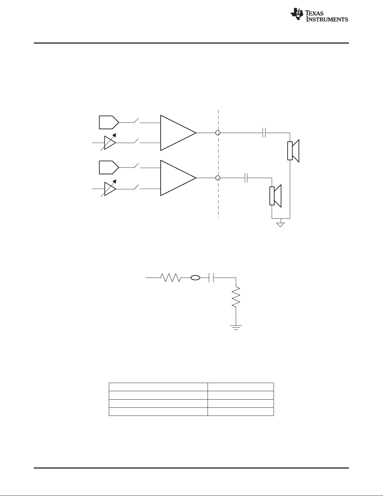
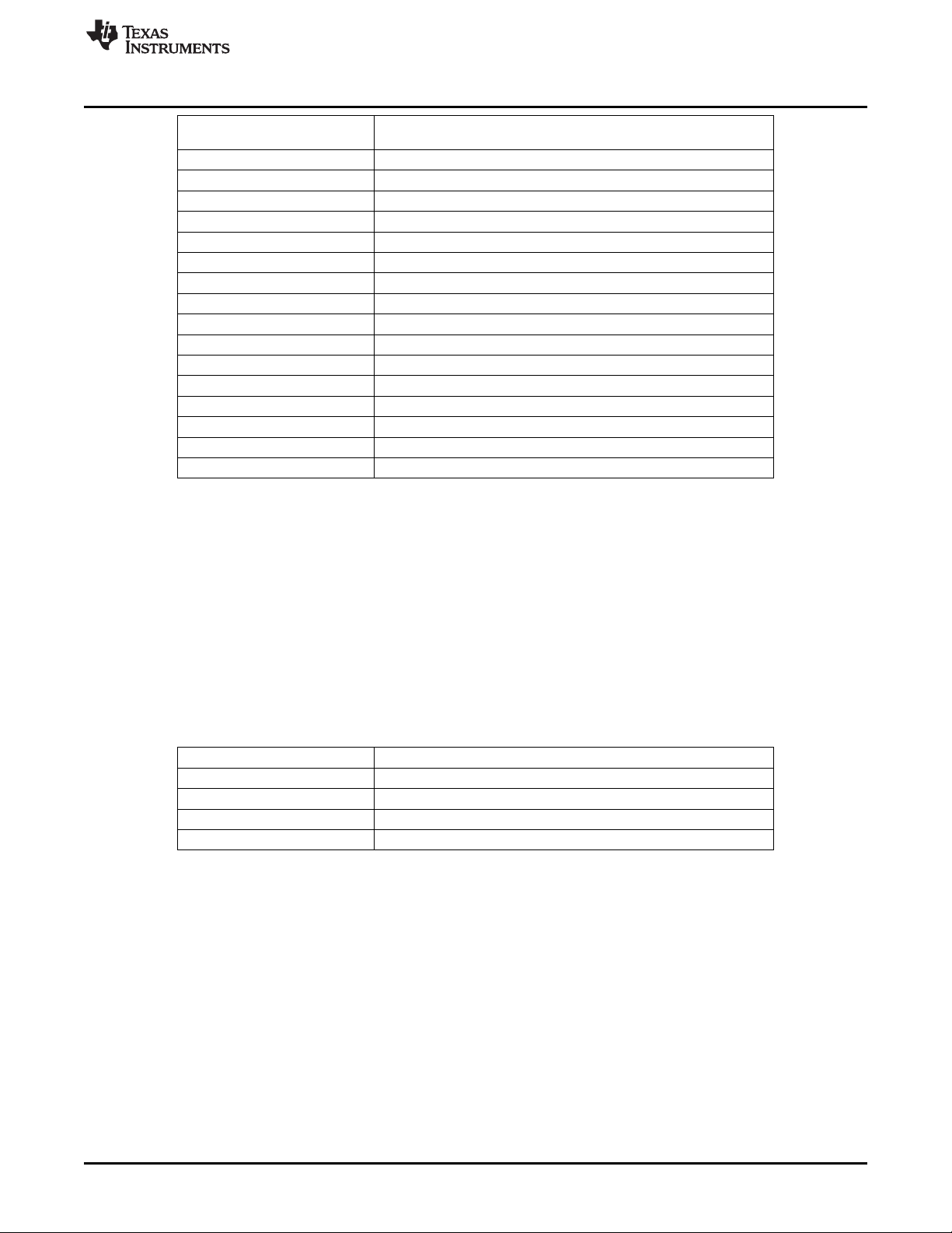
2.2.4 Stereo Single Ended Configuration
Figure 2-2. Stereo Headphone Configuration
The left and right DAC channels are routed to the corresponding left and right headphone amplifier. This
configuration is also used to drive line-level loads.
Figure 2-3. Conceptual Circuit for Pop-Free Power-up
The value of R
(1)
If the device must be placed into 'mute' from the –6.0dB setting, set the device at a gain of –5.0dB first, then place the device into mute.
can be chosen by setting register Page 1, Register 20, Bits D1-D0).
pop
Table 2-3. R
Page 1, Register 20, Bits D1-D0) R
00 2kΩ
01 6kΩ
10 25kΩ
pop
Values
pop
Value
According to the conceptual circuit in Figure 2-3, the voltage on PAD will exponentially settle to the output
common-mode voltage based on the value of R
power-up mode for time T, such that at the end of the slow power-on period, the voltage on V
close to the common-mode voltage. The PCM3070 allows the time T to be adjusted to allow for a wide
range of R
value of Ccis assumed to be 47μF. N=5 is expected to yield good results.
10
PCM3070 Application SLAU332–March 2011
and Cc. Thus, the output drivers must be in slow
and Ccby programming Page 1, Register 20, Bits D5-D2). For the time adjustments, the
load
© 2011, TexasInstruments Incorporated
pop
Submit Documentation Feedback
pad
is very
Page 11
www.ti.com
Analog Audio I/O
Page 1, Register 20, Bits Slow Charging Time=N*Time – Constants(for R
D5-D2)
0000 N=0
0001 N=0.5
0010 N=0.625
0011 N=0.75
0100 N=0.875
0101 N=1.0
0110 N=2.0
0111 N=3.0
1000 N=4.0
1001 N=5.0
1010 N=6.0
1011 N=7.0
1100 N=8.0
1101 N=16 (Not valid for R
1110 N=24 (Not valid for R
1111 N=32 (Not valid for R
Again, for example, for R
=25kΩ)
pop
=25kΩ)
pop
=25kΩ)
pop
=32Ω, Cc=47μF and common mode of 0.9V, the number of time constants
load
and 47μF)
pop
required for pop-free operation is 5 or 6. A higher or lower Ccvalue will require higher or lower value for N.
During the slow-charging period, no signal is routed to the output driver. Therefore, choosing a larger than
necessary value of N results in a delay from power-up to signal at output. At the same time, choosing N to
be smaller than the optimal value results in poor pop performance at power-up.
The signals being routed to headphone drivers (e.g. DAC, MAL , MAR and IN1) often have DC offsets due
to less-than-ideal processing. As a result, when these signals are routed to output drivers, the offset
voltage causes a pop. To improve the pop-performance in such situations, a feature is provided to
soft-step the DC-offset. At the beginning of the signal routing, a high-value attenuation can be applied
which can be progressively reduced in steps until the desired gain in the channel is reached. The time
interval between each of these gain changes can be controlled by programming Page 1, Register 20, Bits
D7-D6). This gain soft-stepping is applied only during the initial routing of the signal to the output driver
and not during subsequent gain changes.
Page 1, Register 20, Bits D7-D6 Soft-stepping Step Time During initial signal routing
00 0 ms (soft-stepping disabled)
01 50ms
10 100ms
11 200ms
It is recommended to use the following sequence for achieving optimal pop performance at power-up:
1. Choose the value of R
, N (time constants) and soft-stepping step time for slow power-up.
pop
2. Choose the configuration for output drivers, including common modes and output stage power
connections
3. Select the signals to be routed to headphones.
4. Power-up the blocks driving signals into HPL and HPR, but keep it muted
5. Unmute HPL and HPR and set the desired gain setting.
6. Power-on the HPL and HPR drivers.
7. Unmute the block driving signals to HPL and HPR after the Driver PGA flags are set to indicate
completion of soft-stepping after power-up. These flags can be read from Page 1, Register 63, Bits
D7-D6).
It is important to configure the Headphone Output driver depop control registers before powering up the
headphone; these register contents should not be changed when the headphone drivers are powered up.
Before powering down the HPL and HPR drivers, it is recommended that user read back the flags in Page
SLAU332–March 2011 PCM3070 Application
Submit Documentation Feedback
© 2011, TexasInstruments Incorporated
11
Page 12
LEFT
DAC
HPL
HPR
LEFT_DACP
LEFT_DACM
Analog Audio I/O
1, Register 63. For example. before powering down the HPL driver, ensure that bit D(7) = 1 and bit D(3) =
1 if INL is routed to HPL and bit D(1) = 1 if the Left Mixer is routed to HPL. The output driver should be
powered down only after a steady-state power-up condition has been achieved. This steady state
power-up condition also must be satisfied for changing the HPL/R driver mute control in Page 1, Register
16 and 17, Bits D7), i.e. muting and unmuting should be done after the gain and volume controls
associated with routing to HPL/R finished soft-stepping.
In the differential configuration of HPL and HPR, when no coupling capacitor is used, the slow charging
method for pop-free performance need not be used. In the differential load configuration for HPL and
HPR, it is recommended to not use the output driver MUTE feature, because a pop may result.
During the power-down state, the headphone outputs are weakly pulled to ground using an approximately
50kΩ resistor to ground, to maintain the output voltage on HPL and HPR pins.
2.2.5 Mono Differential DAC to Mono Differential Headphone Output
www.ti.com
Figure 2-4. Low Power Mono DAC to Differential Headphone
This configuration supports the routing of the two differential outputs of the mono, left channel DAC to the
headphone amplifiers in differential mode (Page 1 / Register 12, D3 =1 and Page 1 / Register 13, D4 =1).
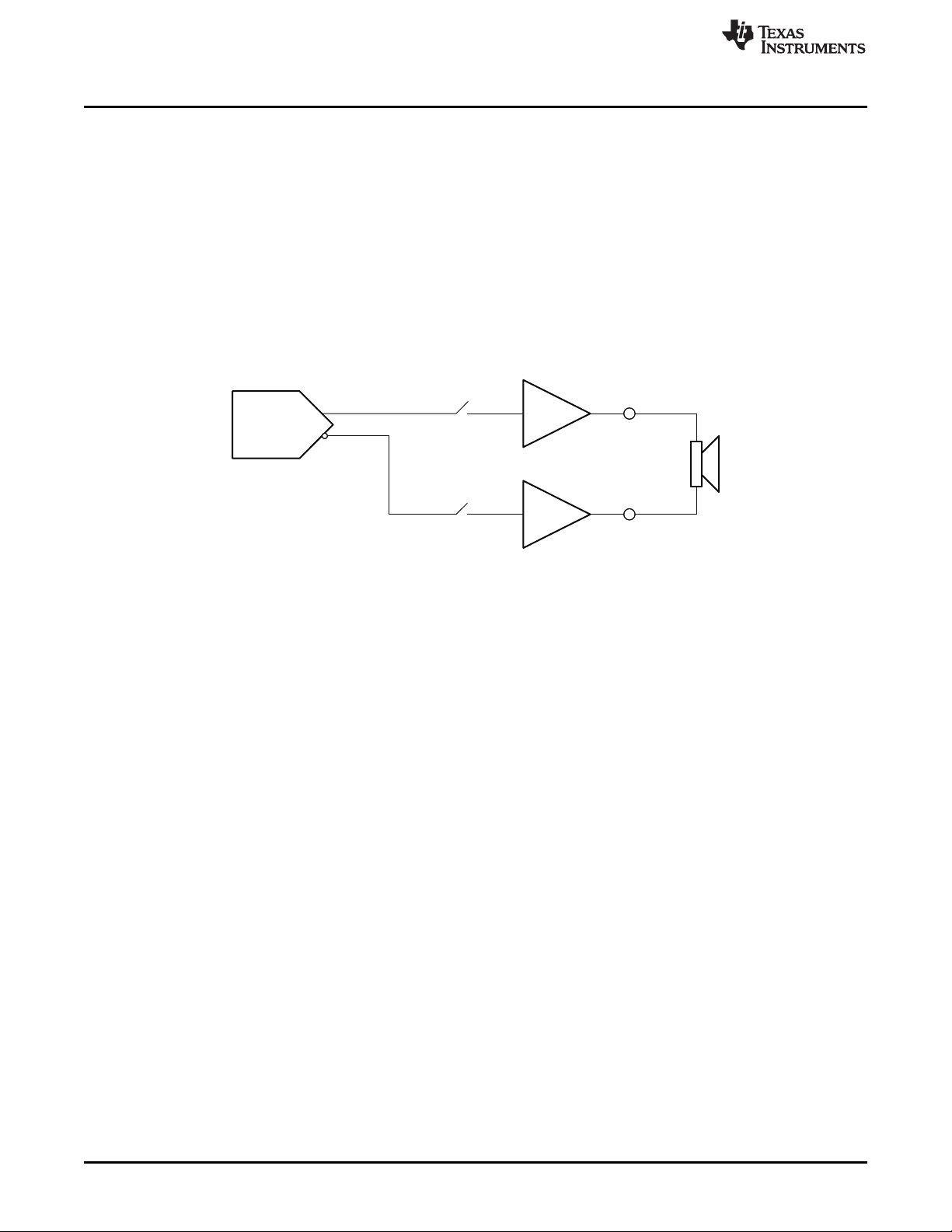
2.2.6 Headphone Amplifier Class-D Mode
By default the headphone amplifiers in the PCM3070 work in Class-AB mode. By writing to Page 1,
Register 3, Bits D7-D6) for the left headphone amplifier, and Page 1, Register 4, Bits D7-D6) with value
11, the headphone amplifiers enter a Class-D mode of operation.
In this mode a high frequency digital pulse-train representation of the DAC signal is fed to the load
connected to HPL and HPR outputs.
Because the output signal is a pulse train switching between Power Supply and Ground, the efficiency of
the amplifier is greatly improved. In this mode however, for good noise performance, care should be taken
to keep the analog power supply clean.
For using the Class-D mode of operation, the following clock-divider condition should be met:
MDAC = I × 4, where I = 1, 2, ..., 32
When a direct digital pulse train is driven out as a signal, high frequencies as a function of pulse train
frequency are also present which lead to power waste. To increase the efficiency and reduce power
dissipation in the load due to these high frequencies, an LC filter should be used in series with the output
and the load. The cutoff frequency of the LC filter should be adjusted to allow audio signals below 20kHz
to pass through, but highly attenuate the high-frequency signal content.
12
PCM3070 Application SLAU332–March 2011
© 2011, TexasInstruments Incorporated
Submit Documentation Feedback
Page 13
L =82 Hm
C =47 FCm
C=1 Fm
Rload=32 W
www.ti.com
Figure 2-5. Configuration for Using Headphone Amplifier in Class-D Mode
For using the headphones in the Class-D mode of operation, the headphones should first be powered up
in default Class-AB mode to charge the AC-coupling capacitor to the set common mode voltage. Once the
headphone amplifiers have been so powered up, the DAC should be routed to headphones and unmuted
before they can be switched to the Class-D mode. After Class D mode has been turned on, the linear,
Class AB mode amplifier must be turned off. For powering down the headphone amplifiers, the DAC
should first be muted.
See Section 4.0.2 for an example setup script enabling Class-D mode.
2.2.7 Line Outputs
The stereo line level drivers on LOL and LOR pins can drive a wide range of line level resistive
impedances in the range of 600Ω to 10kΩ. The output common modes of line level drivers can be
configured to equal either the analog input common-mode setting or to 1.65V. With output common-mode
setting of 1.65V and DRVdd_HP supply at 3.3V the line-level drivers can drive up to 1Vrms output signal.
The line-level drivers can drive out a mixed combination of DAC signal and attenuated ADC PGA signal.
Signal mixing is register-programmable.
ADC
2.3 ADC
The PCM3070 includes a stereo audio ADC, which uses a delta-sigma modulator with a programmable
oversampling ratio, followed by a digital decimation filter. The stereo recording path can be powered up
one channel at a time, to support the case where only mono record capability is required.
The ADC path of the PCM3070 features a large set of options for signal conditioning as well as signal
routing:
• 2 ADCs
• 6 analog inputs which can be mixed and/or multiplexed in single-ended and/or differential configuration
• 2 programmable gain amplifiers (PGA) with a range of 0 to +47.5dB
• 2 mixer amplifiers for analog bypass
• 2 analog bypass channels
• Fine gain adjust of digital channels with 0.1 dB step size
• Digital volume control with a range of -12 to +20dB
• Mute function
• Automatic gain control (AGC)
In addition to the standard set of ADC features the PCM3070 also offers the following special functions:
• Channel-to-channel phase adjustment
• Fast charge of ac-coupling capacitors
• Anti thump
• Adaptive filter mode
Because of the oversampling nature of the audio ADC and the integrated digital decimation filtering,
requirements for analog anti-aliasing filtering are very relaxed. The PCM3070 integrates a second order
analog anti-aliasing filter with 28-dB attenuation at 6MHz. This filter, combined with the digital decimation
filter, provides sufficient anti-aliasing filtering without requiring additional external components.
SLAU332–March 2011 PCM3070 Application
Submit Documentation Feedback
© 2011, TexasInstruments Incorporated
13
Page 14
Analog
Gain
Analog
In
Input
Selection
ADC
Filtering
Digital
Volume
Control
Digital
Gain
Adjust
0...47.5 dB
Step =0.5 dB
0, -6, -12 dB -12...20 dB
Step =0.5 dB
0…-0.4 dB
Step= 0.1 dB
Frequency
Response/
Gain
Fully
Programmable
Coefficients
Audio
Interface
ADC
PGA
ADC
2.3.1 ADC Signal Routing
As shown in Figure 2-1, the PCM3070 includes six analog inputs which can be configured as either 3
stereo single-ended pairs or 3 fully-differential pairs. These pins connect through series resistors and
switches to the virtual ground terminals of two fully-differential amplifiers (one per ADC/PGA channel). By
turning on only one set of switches per amplifier at a time, the inputs can be effectively multiplexed to
each ADC PGA channel. By turning on multiple sets of switches per amplifier at a time, audio sources can
be mixed. The PCM3070 supports the ability to mix up to four single-ended analog inputs or up to two
fully-differential analog inputs into each ADC PGA channel.
The PCM3070 allows the user the flexibility of choosing the input impedance from 10kΩ, 20kΩ and 40kΩ.
When multiple inputs are mixed together, by choosing different input impedances, level adjustment can be
achieved. For example, if one input is selected with 10kΩ input impedance and the second input is
selected with 20kΩ input impedance, then the second input is attenuated by half as compared to the first
input. Note that this input level control is not intended to be a volume control, but instead used
occasionally for level setting.
Mixing of multiple inputs can easily lead to PGA outputs that exceed the range of the internal amplifiers,
resulting in saturation and clipping of the mixed output signal. Whenever mixing is being implemented, the
system designer is advised to take adequate precautions to avoid such a saturation from occurring. In
general, the mixed signal should not exceed 0dB.
Typically, voice or audio signal inputs are capacitively coupled to the device. This allows the device to
independently set the common mode of the input signals to values chosen by register control of Page 1,
Register 10, D(6) to either 0.9V or 0.75V. The correct value maximizes the dynamic range across the
entire analog-supply range. Failure to capacitively connect the input to the device can cause high offset
due to mismatch in source common-mode and device common-mode setting. In extreme cases it could
also saturate the analog channel, causing distortion.
www.ti.com
2.3.2 ADC Gain Setting
When the gain of the ADC Channel is kept at 0dB and the common mode set to 0.75V, a single-ended
input of 0.375V
gain is kept at 0dB, and common mode is set to 0.9V, a single-ended input of 0.5V
full-scale digital signal at the output of the ADC channel. However various block functions control the gain
through the channel. The gain applied by the PGA is described in Table 2-4. Additionally, the digital
volume control adjusts the gain through the channel as described in Section 2.3.2.2. A finer level of gain is
controlled by fine gain control as described in Section 2.3.2.3. The decimation filters A, B and C along with
the delta-sigma modulator contribute to a DC gain of 1.0 through the channel.
2.3.2.1 Analog Programmable Gain Amplifier (PGA)
The PCM3070 features a built-in low-noise PGA for boosting low-level signals to full-scale to achieve high
SNR. This PGA can provide a gain in the range of 0dB to 47.5dB for single-ended inputs or 6dB to 53.5dB
for fully-differential inputs (gain calculated w.r.t. input impedance setting of 10kΩ, 20kΩ input impedance
will result in 6dB lower and 40kΩ will result in 12dB lower gain). This gain can be user controlled by writing
to Page 1, Register 59 and Page 1, Register 60. In the AGC mode this gain can also be automatically
controlled by the built-in hardware AGC.
results in a full-scale digital signal at the output of ADC channel. Similarly, when the
RMS
results in a
RMS
14
PCM3070 Application SLAU332–March 2011
© 2011, TexasInstruments Incorporated
Submit Documentation Feedback
Page 15
www.ti.com
Page 1, EFFECTIVE GAIN APPLIED BY PGA
Register 59, D(6:0)
Page 1,
Register 60, D(6:0)
000 0000 0dB –6dB -12dB 6.0dB 0dB –6.0dB
000 0001 0.5dB –5.5dB –11.5dB 6.5dB 0.5dB -5.5dB
000 0010 1.0dB –5.0dB –11.0dB 7.0dB 7.5dB –5.0dB
… … … … … … …
101 1110 47.0dB 41.0dB 35.0dB 53.0dB 47.0dB 41.0dB
101 1111 47.5dB 41.5dB 35.5dB 53.5dB 47.5dB 41.5dB
The gain changes are implemented with an internal soft-stepping algorithm that only changes the actual
volume level by one 0.5dB step every one or two ADC output samples, depending on the register value
(see registers Page 0, Reg 81, D(1:0)). This soft-stepping ensures that volume control changes occur
smoothly with no audible artifacts. On reset, the PGA gain defaults to a mute condition, and at power
down, the PGA soft-steps the volume to mute before shutting down. A read-only flag Page 0, Reg 36, D(7)
and D(3) is set whenever the gain applied by the PGA equals the desired value set by the register. The
soft-stepping control can also be disabled by programming Page 0, Reg 81, D(1:0).
2.3.2.2 Digital Volume Control
The PCM3070 also has a digital volume-control block with a range from -12dB to +20dB in steps of 0.5dB.
It is set by programming Page 0, Register 83 and 84 respectively for left and right channels.
ADC
Table 2-4. Analog PGA vs Input Configuration
SINGLE-ENDED DIFFERENTIAL
RIN= 10K RIN= 20K RIN= 40K RIN= RIN= RIN= 40K
10K 20K
Table 2-5. Digital Volume Control for ADC
Desired Gain Left / Right Channel
dB Page 1, Register 83/84,
–12.0 110 1000
–11.5 110 1001
–11.0 110 1010
..
–0.5 111 1111
0.0 000 0000 (Default)
+0.5 000 0001
..
+19.5 010 0111
+20.0 010 1000
D(6:0)
During volume control changes, the soft-stepping feature is used to avoid audible artifacts. The
soft-stepping rate can be set to either 1 or 2 gain steps per sample. Soft-stepping can also be entirely
disabled. This soft-stepping is configured via Page 1, Register 81, D(1:0), and is common to soft-stepping
control for the analog PGA. During power-down of an ADC channel, this volume control soft-steps down to
-12.0dB before powering down. Due to the soft-stepping control, soon after changing the volume control
setting or powering down the ADC channel, the actual applied gain may be different from the one
programmed through the control register. The PCM3070 gives feedback to the user, through read-only
flags Page 1, Reg 36, D(7) for Left Channel and Page 1, Reg 36, D(3) for the right channel.
2.3.2.3 Fine Digital Gain Adjustment
Additionally, the gains in each of the channels is finely adjustable in steps of 0.1dB. This is useful when
trying to match the gain between channels. By programming Page 0, Register 82 the gain can be adjusted
from 0dB to -0.4dB in steps of 0.1dB. This feature, in combination with the regular digital volume control
allows the gains through the left and right channels be matched in the range of -0.5dB to +0.5dB with a
resolution of 0.1dB.
SLAU332–March 2011 PCM3070 Application
Submit Documentation Feedback
© 2011, TexasInstruments Incorporated
15
Page 16

ADC
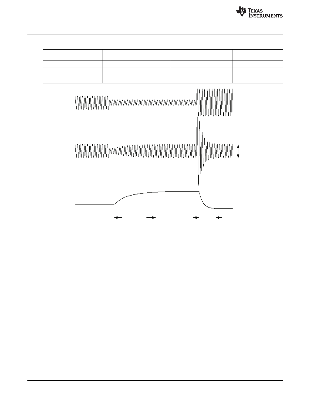
2.3.2.4 AGC
The PCM3070 includes Automatic Gain Control (AGC) for ADC recording. AGC can be used to maintain a
nominally-constant output level. As opposed to manually setting the PGA gain, in the AGC mode, the
circuitry automatically adjusts the PGA gain as the input signal becomes overly loud or very weak. The
AGC algorithm has several programmable parameters, including target gain, attack and decay time
constants, noise threshold, and max PGA applicable, that allow the algorithm to be fine tuned for any
particular application. The algorithm uses the absolute average of the signal (which is the average of the
absolute value of the signal) as a measure of the nominal amplitude of the output signal. Since the gain
can be changed at the sample interval time, the AGC algorithm operates at the ADC sample rate.
1. Target Level represents the nominal output level at which the AGC attempts to hold the ADC output
signal level. The PCM3070 allows programming of eight different target levels, which can be
programmed from –5.5dB to –24dB relative to a full-scale signal. Since the PCM3070 reacts to the
signal absolute average and not to peak levels, it is recommended that the target level be set with
enough margin to avoid clipping at the occurrence of loud sounds.
2. Attack Time determines how quickly the AGC circuitry reduces the PGA gain when the output signal
level exceeds the target level due to increase in input signal level. Wide range of attack time
programmability is supported in terms of number of samples (i.e. number of ADC sample frequency
clock cycles).
3. Decay Time determines how quickly the PGA gain is increased when the output signal level falls
below the target level due to reduction in input signal level. Wide range of decay time programmability
is supported in terms of number of samples (i.e., number of ADC sample frequency clock cycles).
4. Gain Hysteresis is the hysteresis applied to the required gain calculated by the AGC function while
changing its mode of operation from attack to decay or vice-versa. For example, while attacking the
input signal, if the current applied gain by the AGC is xdB, and suddenly because of input level going
down, the new calculated required gain is ydB, then this gain is applied provided y is greater than x by
the value set in Gain Hysteresis. This feature avoids the condition when the AGC function can fluctuate
between a very narrow band of gains leading to audible artifacts. The Gain Hysteresis can be adjusted
or disabled by the user.
5. Noise threshold determines the level below which if the input signal level falls, the AGC considers it
as silence, and thus brings down the gain to 0dB in steps of 0.5dB every FS and sets the noise
threshold flag. The gain stays at 0dB unless the input speech signal average rises above the noise
threshold setting. This ensures that noise is not 'gained up' in the absence of speech. Noise threshold
level in the AGC algorithm is programmable from -30dB to -90dB of full-scale. When AGC Noise
Threshold is set to –70dB, –80db, or –90dB, the microphone input Max PGA applicable setting must
be greater than or equal to 11.5dB, 21.5dB, or 31.5dB respectively. This operation includes hysteresis
and debounce to avoid the AGC gain from cycling between high gain and 0dB when signals are near
the noise threshold level. The noise (or silence) detection feature can be entirely disabled by the user.
6. Max PGA applicable allows the designer to restrict the maximum gain applied by the AGC. This can
be used for limiting PGA gain in situations where environmental noise is greater than the programmed
noise threshold. Microphone input Max PGA can be programmed from 0dB to 58dB in steps of 0.5dB.
7. Hysteresis, as the name suggests, determines a window around the Noise Threshold which must be
exceeded to either detect that the recorded signal is indeed noise or signal. If initially the energy of the
recorded signal is greater than the Noise Threshold, then the AGC recognizes it as noise only when
the energy of the recorded signal falls below the Noise Threshold by a value given by Hysteresis.
Similarly, after the recorded signal is recognized as noise, for the AGC to recognize it as a signal, its
energy must exceed the Noise Threshold by a value given by the Hysteresis setting. In order to
prevent the AGC from jumping between noise and signal states, (which can happen when the energy
of recorded signal is very close to the Noise threshold) a non-zero hysteresis value should be chosen.
The Hysteresis feature can also be disabled.
8. Debounce Time (Noise and Signal) determines the hysteresis in time domain for noise detection.
The AGC continuously calculates the energy of the recorded signal. If the calculated energy is less
than the set Noise Threshold, then the AGC does not increase the input gain to achieve the Target
Level. However, to handle audible artifacts which can occur when the energy of the input signal is very
close to the Noise Threshold, the AGC checks if the energy of the recorded signal is less than the
Noise Threshold for a time greater than the Noise Debounce Time. Similarly the AGC starts increasing
the input-signal gain to reach the Target Level when the calculated energy of the input signal is greater
than the Noise Threshold. Again, to avoid audible artifacts when the input-signal energy is very close
to Noise Threshold, the energy of the input signal needs to continuously exceed the Noise Threshold
www.ti.com
16
PCM3070 Application SLAU332–March 2011
Submit Documentation Feedback
© 2011, TexasInstruments Incorporated
Page 17
1
1
23
1
10
zD2
zNN
)z(H
-
-
-
+
=
www.ti.com
9. The AGC Noise Threshold Flag is a read-only flag indicating that the input signal has levels lower
10. Gain Applied by AGC is a ready-only register setting which gives a real-time feedback to the system
11. The AGC Saturation Flag is a read-only flag indicating that the ADC output signal has not reached its
12. The ADC Saturation Flag is a read-only flag indicating an overflow condition in the ADC channel. On
13. An AGC low-pass filter is used to help determine the average level of the input signal. This average
ADC
value for the Signal Debounce Time. If the debounce times are kept very small, then audible artifacts
can result by rapid enabling and disabling the AGC function. At the same time, if the Debounce time is
kept too large, then the AGC may take time to respond to changes in levels of input signals with
respect to Noise Threshold. Both noise and signal debounce time can be disabled.
than the Noise Threshold, and thus is detected as noise (or silence). In such a condition the AGC
applies a gain of 0dB.
on the gain applied by the AGC to the recorded signal. This, along with the Target Setting, can be
used to determine the input signal level. In a steady state situation
Target Level (dB ) = Gain Applied by AGC (dB) + Input Signal Level (dB)
When the AGC noise threshold flag is set, then the status of gain applied by AGC should be ignored.
Target Level. However, the AGC is unable to increase the gain further because the required gain is
higher than the Maximum Allowed PGA gain. Such a situation can happen when the input signal has
very low energy and the Noise Threshold is also set very low. When the AGC noise threshold flag is
set, the status of AGC saturation flag should be ignored.
overflow, the signal is clipped and distortion results. This typically happens when the AGC Target Level
is kept very high and the energy in the input signal increases faster than the Attack Time.
level is compared to the programmed detection levels in the AGC to provide the correct functionality.
This low pass filter is in the form of a first-order IIR filter. Three 8-bit registers are used to form the
24-bit digital coefficient as shown on the register map. In this way, a total of 9 registers are
programmed to form the 3 IIR coefficients. The transfer function of the filter implemented for signal
level detection is given by
Where:
Coefficient N0 can be programmed by writing into Page 8, Register 12, 13 and 14.
Coefficient N1 can be programmed by writing into Page 8, Register 16, 17 and 18.
Coefficient D1 can be programmed by writing into Page 8, Register 20, 21 and 22.
N0, N1 and D1 are 24-bit 2’s complement numbers and their default values implement a low-pass
filter with cut-off at 0.002735*ADC_FS .
See Table 2-6 for various AGC programming options. AGC can be used only if analog microphone
input is routed to the ADC channel.
Table 2-6. AGC Parameter Settings
Function Control Register Control Register Bit
Left ADC Right ADC
AGC enable Page 0, Register 86 Page 0,Register 94 D(7)
Target Level Page 0, Register 86 Page 0, Register 94 D(6:4)
Gain Hysteresis Page 0, Register 86 Page 0, Register 94 D(1:0)
Hysteresis Page 0, Register 87 Page 0, Register 95 D(7:6)
Noise threshold Page 0, Register 87 Page 0, Register 95 D(5:1)
Max PGA applicable Page 0, Register 88 Page 0, Register 96 D(6:0)
Time constants (attack time) Page 0, Register 89 Page 0, Register 97 D(7:0)
Time constants(decay time) Page 0, Register 90 Page 0, Register 98 D(7:0)
Debounce time (Noise) Page 0, Register 91 Page 0, Register 99 D(4:0)
Debounce time (Signal) Page 0, Register 92 Page 0, Register 100 D(3:0)
Gain applied by AGC Page 0, Register 93 Page 0, Register 101 D(7:0) (Read Only)
AGC Noise Threshold Flag Page 0, Register 45 (sticky flag), Page 0, Register 45 (sticky flag), D(6:5) (Read Only)
Page 0, Register 47 (non-sticky Page 0, Register 47 (non-sticky
flag) flag)
(1)
SLAU332–March 2011 PCM3070 Application
Submit Documentation Feedback
© 2011, TexasInstruments Incorporated
17
Page 18
DecayTime
Target
Level
Input
Signal
Output
Signal
AGC
Gain
Attack
Time
ADC
www.ti.com
Table 2-6. AGC Parameter Settings (continued)
Function Control Register Control Register Bit
Left ADC Right ADC
AGC Saturation flag Page 0, Register 36 (sticky flag) Page 0, Register 36 (sticky flag) D(5), D(1) (Read Only)
ADC Saturation flag Page 0, Register 42 (sticky flag), Page 0, Register 42 (sticky flag), D(3:2) (Read Only)
Page 0, Register 43 (non-sticky Page 0, Register 43 (non-sticky
flag) flag)
Figure 2-6. AGC Characteristics
2.3.3 ADC Decimation Filtering and Signal Processing Overview
The PCM3070 ADC channel includes a built-in digital decimation filter to process the oversampled data
from the sigma-delta modulator to generate digital data at Nyquist sampling rate with high dynamic range.
The decimation filter can be chosen from three different types, depending on the required frequency
response, group delay and sampling rate.
2.3.4 ADC Processing Blocks
The PCM3070 offers a range of processing blocks which implement various signal processing capabilities
along with decimation filtering. These processing blocks give users the choice of how much and what type
of signal processing they may use and which decimation filter is applied.
Table 2-7 gives an overview of the available processing blocks of the ADC channel and their properties.
The signal processing blocks available are:
• First-order IIR
• Scalable number of biquad filters
• Variable-tap FIR filter
• AGC
18
PCM3070 Application SLAU332–March 2011
Submit Documentation Feedback
© 2011, TexasInstruments Incorporated
Page 19
ToAudio
Interface
1stOrder
IIR
´
AGC
Gain
Compen-
sation
AGC
ToAnalog PGA
Filter A
From Delta-Sigma
Modulator
From Digital Vol. Ctrl
www.ti.com
The processing blocks are tuned for common cases and can achieve high anti-alias filtering or low-group
delay in combination with various signal processing effects such as audio effects and frequency shaping.
The available first order IIR, BiQuad and FIR filters have fully user-programmable coefficients. The
Resource Class Column (RC) gives an approximate indication of power consumption.
(1)
ADC
Table 2-7. ADC Processing Blocks
Processing Channel Decimation 1st Order Number FIR Required Resource
Blocks Filter IIR BiQuads AOSR Value Class
PRB_R1
(1)
Stereo A Yes 0 No 128,64 6
PRB_R2 Stereo A Yes 5 No 128,64 8
PRB_R3 Stereo A Yes 0 25-Tap 128,64 8
PRB_R4 Right A Yes 0 No 128,64 3
PRB_R5 Right A Yes 5 No 128,64 4
PRB_R6 Right A Yes 0 25-Tap 128,64 4
PRB_R7 Stereo B Yes 0 No 64 3
PRB_R8 Stereo B Yes 3 No 64 4
PRB_R9 Stereo B Yes 0 20-Tap 64 4
PRB_R10 Right B Yes 0 No 64 2
PRB_R11 Right B Yes 3 No 64 2
PRB_R12 Right B Yes 0 20-Tap 64 2
PRB_R13 Stereo C Yes 0 No 32 3
PRB_R14 Stereo C Yes 5 No 32 4
PRB_R15 Stereo C Yes 0 25-Tap 32 4
PRB_R16 Right C Yes 0 No 32 2
PRB_R17 Right C Yes 5 No 32 2
PRB_R18 Right C Yes 0 25-Tap 32 2
Default
Available
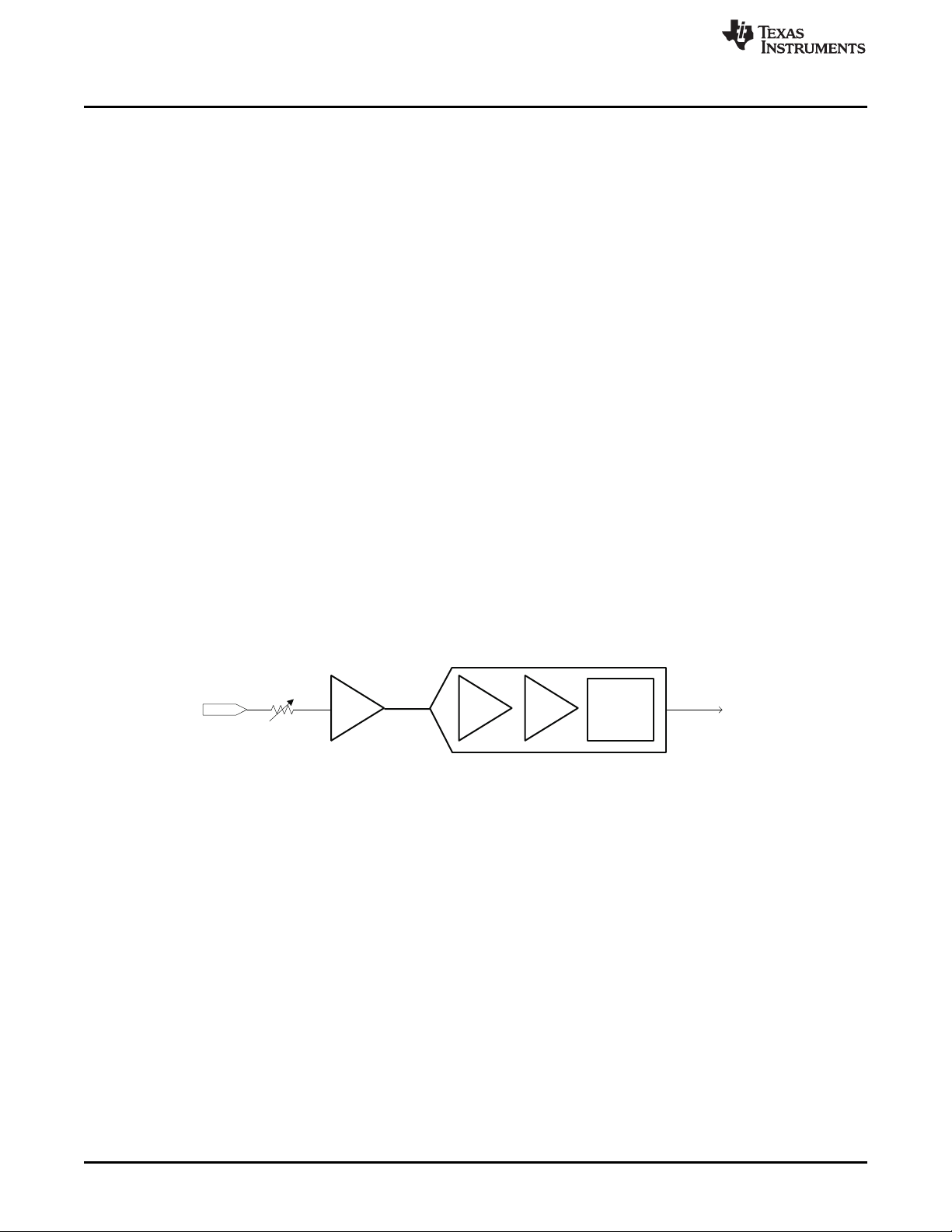
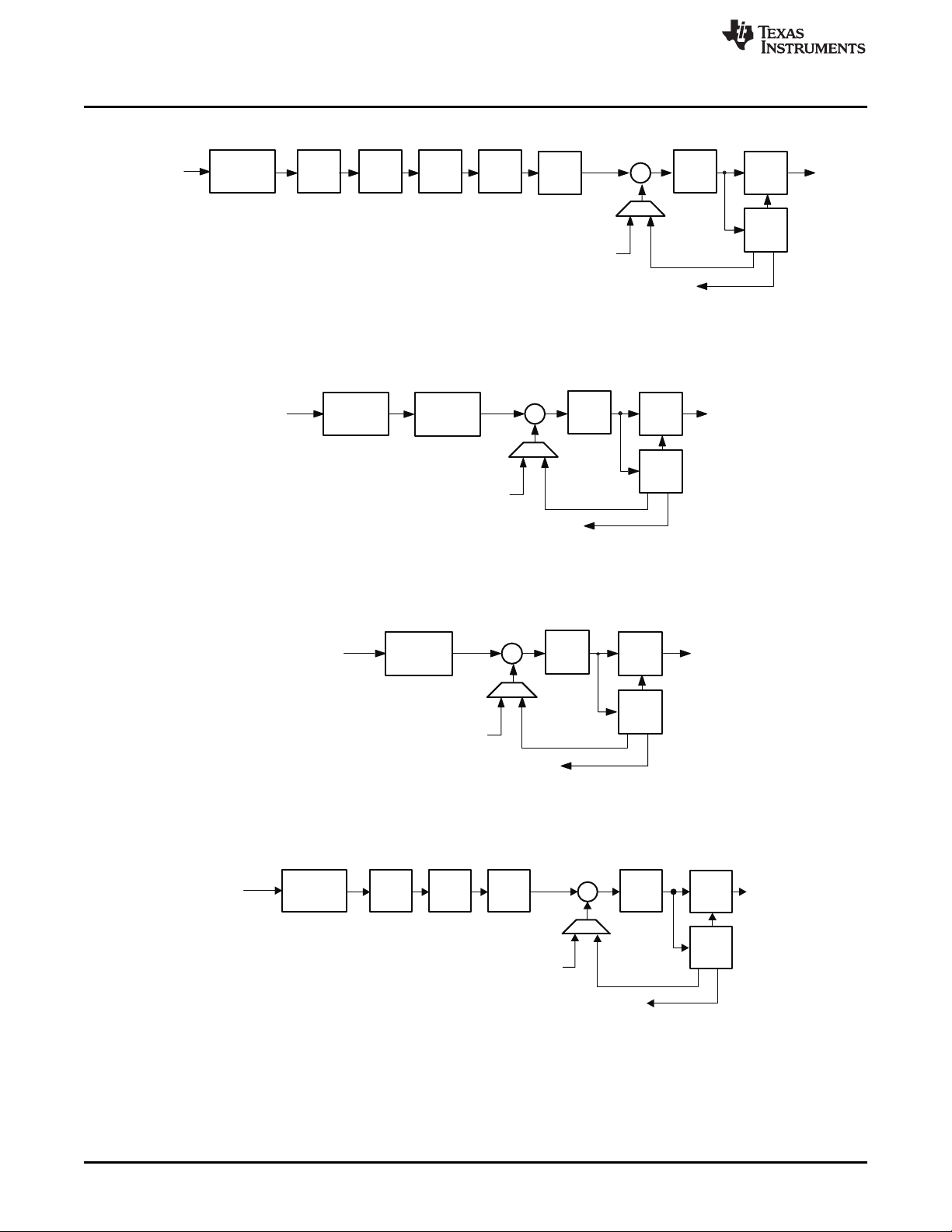
2.3.5 Signal Processing Blocks – Details
2.3.5.1 1storder IIR, AGC, Filter A
Figure 2-7. Signal Chain for PRB_R1 and PRB_R4
SLAU332–March 2011 PCM3070 Application
Submit Documentation Feedback
© 2011, TexasInstruments Incorporated
19
Page 20
1stOrder
IIR
AGC
Gain
Compen-
sation
AGC
Filter A
H
E
H
D
H
C
H
B
H
A
ToAudio
Interface
ToAnalog PGA
From Delta-Sigma
Modulator
´
From Digital Vol. Ctrl
1stOrder
IIR
AGC
Gain
Compen-
sation
AGC
Filter A
25-Tap FIR
From Delta-Sigma
Modulator
ToAnalog PGA
ToAudio
Interface
´
From Digital Vol. Ctrl
ToAudio
Interface
1stOrder
IIR
AGC
Gain
Compen-
sation
AGC
Filter B
ToAudio
Interface
ToAnalog PGA
From Delta-Sigma
Modulator
´
From Digital Vol. Ctrl
1stOrder
IIR
AGC
Gain
Compen-
sation
AGC
Filter B H
C
H
B
H
A
From Delta-Sigma
Modulator
ToAnalog PGA
ToAudio
Interface
´
From Digital Vol. Ctrl
ADC
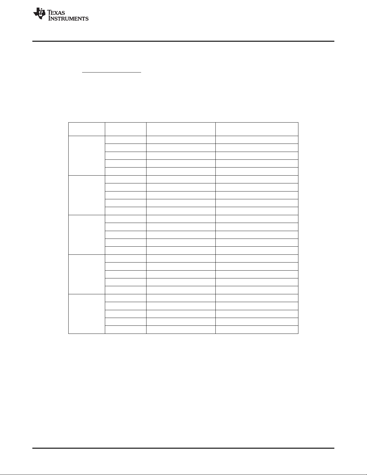
2.3.5.2 5 Biquads, 1storder IIR, AGC, Filter A
Figure 2-8. Signal Chain PRB_R2 and PRB_R5
2.3.5.3 25 Tap FIR, 1storder IIR, AGC, Filter A
www.ti.com
Figure 2-9. Signal Chain for PRB_R3 and PRB_R6
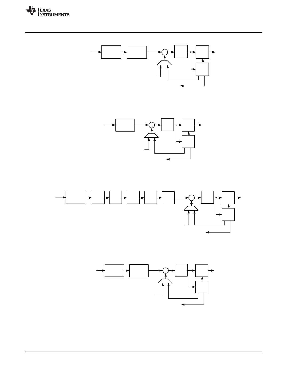
2.3.5.4 1storder IIR, AGC, Filter B
Figure 2-10. Signal Chain for PRB_R7 and PRB_R10
2.3.5.5 3 Biquads, 1storder IIR, AGC, Filter B
20
Figure 2-11. Signal Chain for PRB_R8 and PRB_R11
PCM3070 Application SLAU332–March 2011
© 2011, TexasInstruments Incorporated
Submit Documentation Feedback
Page 21
1stOrder
IIR
AGC
Gain
Compen-
sation
AGC
Filter B
20-Tap FIR
From Delta-Sigma
Modulator
To Analog PGA
ToAudio
Interface
´
From Digital Vol. Ctrl
1stOrder
IIR
AGC
Gain
Compen-
sation
AGC
Filter C
From Delta-Sigma
Modulator
From Digital Vol. Ctrl
ToAnalog PGA
ToAudio
Interface
´
1stOrder
IIR
AGC
Gain
Compen-
sation
AGC
Filter C
H
E
H
D
H
C
H
B
H
A
From Delta-Sigma
Modulator
From Digital Vol. Ctrl
ToAnalog PGA
ToAudio
Interface
´
1stOrder
IIR
AGC
Gain
Compen
sation
AGC
Filter C
25-Tap FIR
From Delta-Sigma
Modulator
From Digital Vol. Ctrl
To Analog PGA
To Audio
Interface
´
www.ti.com
2.3.5.6 20 Tap FIR, 1storder IIR, AGC, Filter B
Figure 2-12. Signal Chain for PRB_R9 and PRB_R12
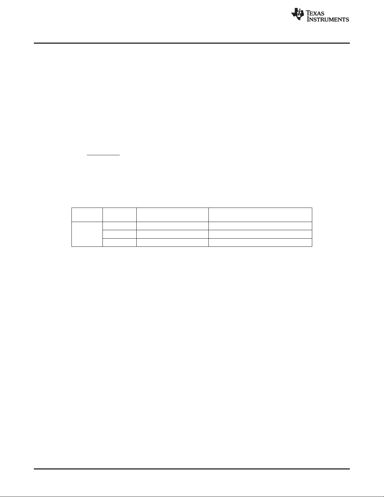
2.3.5.7 1storder IIR, AGC, Filter C
ADC
Figure 2-13. Signal Chain for PRB_R13 and PRB_R16
2.3.5.8 5 Biquads, 1storder IIR, AGC, Filter C
Figure 2-14. Signal Chain for PRB_R14 and PRB_R17
2.3.5.9 25 Tap FIR, 1storder IIR, AGC, Filter C
SLAU332–March 2011 PCM3070 Application
Submit Documentation Feedback
Figure 2-15. Signal for PRB_R15 and PRB_R18
© 2011, TexasInstruments Incorporated
21
Page 22
1
1
23
1
10
zD2
zNN
)z(H
-
-
-
+
=
ADC
2.3.5.10 User Programmable Filters
Depending on the selected processing block, different types and orders of digital filtering are available. A
1st-order IIR filter is always available, and is useful to efficiently filter out possible DC components of the
signal. Up to 5 biquad section or alternatively up to 25-tap FIR filters are available for specific processing
blocks. The coefficients of the available filters are arranged as sequentially indexed coefficients in two
banks. If adaptive filtering is chosen, the coefficient banks can be switched on-the-fly. For more details on
adaptive filtering see Section 2.3.6.5 below.
The coefficients of these filters are each 24-bits wide, in two's-complement and occupy 3 consecutive 8-bit
registers in the register space. For default values please see Section 5.13.
2.3.5.10.1 1stOrder IIR Section
The transfer function for the first order IIR Filter is given by
The frequency response for the 1storder IIR Section with default coefficients is flat at a gain of 0dB.
Details on ADC coefficient default values are given in Section 5.13.
Table 2-8. ADC 1st order IIR Filter Coefficients
www.ti.com
(2)
Filter FIlter ADC Coefficient Left ADC Coefficient Right Channel
1stOrder IIR N1 C5 (Pg 8,Reg 28,29,30) C37 (Pg 9,Reg 36,37,38)
Coefficient Channel
N0 C4 (Pg 8,Reg 24,25,26) C36 (Pg 9,Reg 32,33,34)
D1 C6 (Pg 8,Reg 32,33,34) C39 (Pg 9,Reg 40,41,42)
22
PCM3070 Application SLAU332–March 2011
© 2011, TexasInstruments Incorporated
Submit Documentation Feedback
Page 23
2
2
1
1
23
2
2
1
10
zDzD*22
zNzN*2N
)z(H
--
--
--
++
=
www.ti.com
2.3.5.10.2 Biquad Section
The transfer function of each of the Biquad Filters is given by
The frequency response for each of the biquad section with default coefficients is flat at a gain of 0dB.
Details on ADC coefficient default values are given in Section 5.13.
ADC
(3)
Table 2-9. ADC Biquad Filter Coefficients
Filter FIlter ADC Coefficient Left ADC Coefficient Right Channel
BIQUAD A N0 C7 (Pg 8, Reg 36,37,38) C39 (Pg 9, Reg 44,45,46)
BIQUAD B N0 C12 (Pg 8, Reg 56,57,58) C44 (Pg 9, Reg 64,65,66)
BIQUAD C N0 C17 (Pg 8, Reg 76,77,78) C49 (Pg 9, Reg 84,85,86)
BIQUAD D N0 C22 (Pg 8, Reg 96,97,98) C54 (Pg 9, Reg 104,105,106)
BIQUAD E N0 C27 (Pg 8, Reg 116,117,118) C59 (Pg 9, Reg 124,125,126)
Coefficient Channel
N1 C8 (Pg 8, Reg 40,41,42) C40 (Pg 9, Reg 48,49,50)
N2 C9 (Pg 8, Reg 44,45,46) C41 (Pg 9, Reg 52,53,54)
D1 C10 (Pg 8, Reg 48,49,50) C42 (Pg 9, Reg 56,57,58)
D2 C11 (Pg 8, Reg 52,53,54) C43 (Pg 9, Reg 60,61,62)
N1 C13 (Pg 8, Reg 60,61,62) C45 (Pg 9, Reg 68,69,70)
N2 C14 (Pg 8, Reg 64,65,66) C46 (Pg 9, Reg 72,73,74)
D1 C15 (Pg 8, Reg 68,69,70) C47 (Pg 9, Reg 76,77,78)
D2 C16 (Pg 8, Reg 72,73,74) C48 (Pg 9, Reg 80,81,82)
N1 C18 (Pg 8, Reg 80,81,82) C50 (Pg 9, Reg 88,89,90)
N2 C19 (Pg 8, Reg 84,85,86) C51 (Pg 9, Reg 92,93,94)
D1 C20 (Pg 8, Reg 88,89,90) C52 (Pg 9, Reg 96,97,98)
D2 C21 (Pg 8, Reg 92,93,94) C53 (Pg 9, Reg 100,101,102)
N1 C23 (Pg 8, Reg 100,101,102) C55 (Pg 9, Reg 108,109,110)
N2 C24 (Pg 8, Reg 104,105,106) C56 (Pg 9, Reg 112,113,114)
D1 C25 (Pg 8, Reg 108,109,110) C57 (Pg 9, Reg 116,117,118)
D2 C26 (Pg 8, Reg 112,113,114) C58 (Pg 9, Reg 120,121,122)
N1 C28 (Pg 8, Reg 120,121,122) C60 (Pg 10, Reg 8,9,10)
N2 C29 (Pg 8, Reg 124,125,126) C61 (Pg 10, Reg 12,13,14)
D1 C30 (Pg 9, Reg 8,9,10) C62 (Pg 10, Reg 16,17,18)
D2 C31 (Pg 9, Reg 12,13,14) C63 (Pg 10, Reg 20,21,22)
SLAU332–March 2011 PCM3070 Application
Submit Documentation Feedback
© 2011, TexasInstruments Incorporated
23
Page 24
PRB_R12andPRB_R9for,19M
PRB_R18andPRB_R15PRB_R6,PRB_R3,for,24M
zFir)z(H
M
0n
n
n
=
=
=
å
=
-
ADC
2.3.5.10.3 FIR Section
Six of the available ADC processing blocks offer FIR filters for signal processing. PRB_R9 and PRB_R12
feature a 20-tap FIR filter while the processing blocks PRB_R3, PRB_R6, PRB_R15 and PRB_R18
feature a 25-tap FIR filter
The coefficients of the FIR filters are 24-bit 2’s complement format and correspond to the ADC coefficient
space as listed below. There is no default transfer function for the FIR filter. When the FIR filter gets used
all applicable coefficients must be programmed.
www.ti.com
(4)
Table 2-10. ADC FIR Filter Coefficients
Filter FIlter Coefficient Left ADC Filter Coefficient Right ADC Channel
Fir0 C7 (Pg 8, Reg 36,37,38) C39 (Pg 9, Reg 44,45,46)
Fir1 C8 (Pg 8, Reg 40,41,42) C40 (Pg 9, Reg 48,49,50)
Fir2 C9 (Pg 8, Reg 44,45,46) C41 (Pg 9, Reg 52,53,54)
Fir3 C10 (Pg 8, Reg 48,49,50) C42 (Pg 9, Reg 56,57,58)
Fir4 C11 (Pg 8, Reg 52,53,54) C43 (Pg 9, Reg 60,61,62)
Fir5 C12 (Pg 8, Reg 56,57,58) C44 (Pg 9, Reg 64,65,66)
Fir6 C13 (Pg 8, Reg 60,61,62) C45 (Pg 9, Reg 68,69,70)
Fir7 C14 (Pg 8, Reg 64,65,66) C46 (Pg 9, Reg 72,73,74)
Fir8 C15 (Pg 8, Reg 68,69,70) C47 (Pg 9, Reg 76,77,78)
Fir9 C16 (Pg 8, Reg 72,73,74) C48 (Pg 9, Reg 80,81,82)
Fir10 C17 (Pg 8, Reg 76,77,78) C49 (Pg 9, Reg 84,85,86)
Fir11 C18 (Pg 8, Reg 80,81,82) C50 (Pg 9, Reg 88,89,90)
Fir12 C19 (Pg 8, Reg 84,85,86) C51 (Pg 9, Reg 92,93,94)
Fir13 C20 (Pg 8, Reg 88,89,90) C52 (Pg 9, Reg 96,97,98)
Fir14 C21 (Pg 8, Reg 92,93,94) C53 (Pg 9, Reg 100,101,102)
Fir15 C22 (Pg 8, Reg 96,97,98) C54 (Pg 9, Reg 104,105,106)
Fir16 C23 (Pg 8, Reg 100,101,102) C55 (Pg 9, Reg 108,109,110)
Fir17 C24 (Pg 8, Reg 104,105,106) C56 (Pg 9, Reg 112,113,114)
Fir18 C25 (Pg 8, Reg 108,109,110) C57 (Pg 9, Reg 116,117,118)
Fir19 C26 (Pg 8, Reg 112,113,114) C58 (Pg 9, Reg 120,121,122)
Fir20 C27 (Pg 8, Reg 116,117,118) C59 (Pg 9, Reg 124,125,126)
Fir21 C28 (Pg 8, Reg 120,121,122) C60 (Pg 10, Reg 8,9,10)
Fir22 C29 (Pg 8, Reg 124,125,126) C61 (Pg 10, Reg 12,13,14)
Fir23 C30 (Pg 9, Reg 8,9,10) C62 (Pg 10, Reg 16,17,18)
Fir24 C31 (Pg 9, Reg 12,13,14) C63 (Pg 10, Reg 20,21,22)
Channel
24
PCM3070 Application SLAU332–March 2011
© 2011, TexasInstruments Incorporated
Submit Documentation Feedback
Page 25
0
–10
–20
–30
–40
–50
–60
–70
–80
–90
–100
0.0 0.2 0.4 0.6 0.8 1.0 1.2 1.4 1.6 1.8 2.0
FrequencyNormalizedtof
S
Magnitude – dB
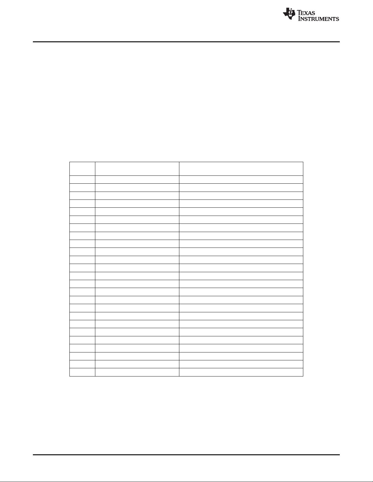
ADCChannelResponseforDecimationFilter A
(Redlinecorrespondsto –73dB)
G013
www.ti.com
2.3.5.11 Decimation Filter
The PCM3070 offers 3 different types of decimation filters. The integrated digital decimation filter removes
high-frequency content and down samples the audio data from an initial sampling rate of AOSR*Fs to the
final output sampling rate of Fs. The decimation filtering is achieved using a higher-order CIC filter
followed by linear-phase FIR filters. The decimation filter cannot be chosen by itself, it is implicitly set
through the chosen processing block.
The following subsections describe the properties of the available filters A, B and C.
2.3.5.11.1 Decimation Filter A
This filter is intended for use at sampling rates up to 48kHz. When configuring this filter, the oversampling
ratio of the ADC can either be 128 or 64. For highest performance the oversampling ratio must be set to
128.
Filter A can also be used for 96kHz at an AOSR of 64.
Parameter Condition Value (Typical) Units
AOSR = 128
Filter Gain Pass Band 0…0.39 Fs 0.062 dB
Filter Gain Stop Band 0.55…64Fs –73 dB
Filter Group Delay 17/Fs Sec.
Pass Band Ripple, 8 ksps 0…0.39 Fs 0.062 dB
Pass Band Ripple, 44.1 ksps 0…0.39 Fs 0.05 dB
Pass Band Ripple, 48 ksps 0…0.39 Fs 0.05 dB
AOSR = 64
Filter Gain Pass Band 0…0.39 Fs 0.062 dB
Filter Gain Stop Band 0.55…32Fs –73 dB
Filter Group Delay 17/Fs Sec.
Pass Band Ripple, 8 ksps 0…0.39 Fs 0.062 dB
Pass Band Ripple, 44.1 ksps 0…0.39 Fs 0.05 dB
Pass Band Ripple, 48 ksps 0…0.39 Fs 0.05 dB
Pass Band Ripple, 96 ksps 0…20kHz 0.1 dB
ADC
Table 2-11. ADC Decimation Filter A, Specification
SLAU332–March 2011 PCM3070 Application
Submit Documentation Feedback
Figure 2-16. ADC Decimation Filter A, Frequency Response
25
© 2011, TexasInstruments Incorporated
Page 26
0
–10
–20
–30
–40
–50
–60
–70
–80
–90
0.0 0.2 0.4 0.6 0.8 1.0 1.2 1.4 1.6 1.8 2.0
FrequencyNormalizedtof
S
Magnitude – dB
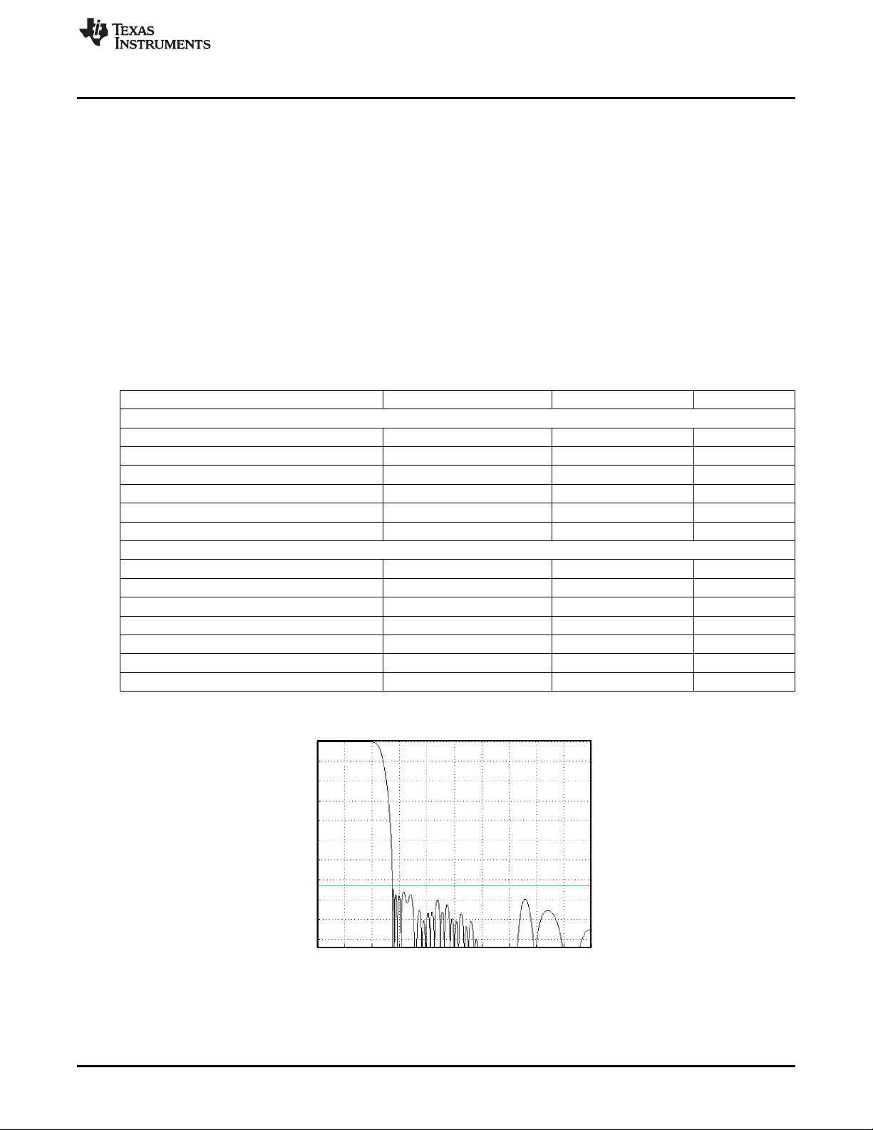
ADCChannelResponseforDecimationFilterB
(Redlinecorrespondsto –44dB)
G014
ADC
2.3.5.11.2 Decimation Filter B
Filter B is intended to support sampling rates up to 96kHz at a oversampling ratio of 64.
Parameter Condition Value (Typical) Units
AOSR = 64
Filter Gain Pass Band 0…0.39Fs ±0.077 dB
Filter Gain Stop Band 0.60Fs…32Fs –46 dB
Filter Group Delay 11/Fs Sec.
Pass Band Ripple, 8 ksps 0…0.39Fs 0.076 dB
Pass Band Ripple, 44.1 ksps 0…0.39Fs 0.06 dB
Pass Band Ripple, 48 ksps 0…0.39Fs 0.06 dB
Pass Band Ripple, 96 ksps 0…20kHz 0.11 dB
www.ti.com
Table 2-12. ADC Decimation Filter B, Specifications
Figure 2-17. ADC Decimation Filter B, Frequency Response
26
PCM3070 Application SLAU332–March 2011
© 2011, TexasInstruments Incorporated
Submit Documentation Feedback
Page 27
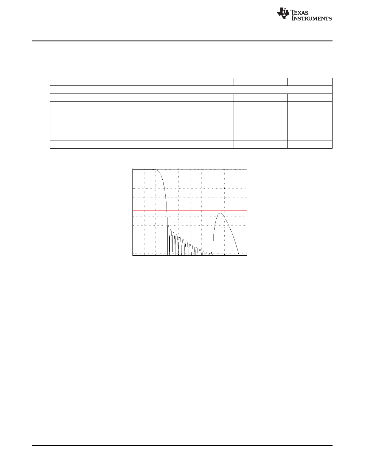
ADCChannelResponseforDecimationFilterC
(Redlinecorrespondsto –60dB)
0
–20
–40
–60
–100
–80
–120
0.0 0.2 0.4 0.6 0.8 1.0 1.2 1.4 1.6 1.8 2.0
FrequencyNormalizedtof
S
Magnitude – dB
G015
www.ti.com
2.3.5.11.3 Decimation Filter C
Filter type C along with AOSR of 32 is specially designed for 192ksps operation for the ADC. The pass
band which extends up to 0.11*Fs ( corresponds to 21kHz), is suited for audio applications.
Parameter Condition Value (Typical) Units
Filter Gain from 0 to 0.11Fs 0…0.11Fs ±0.033 dB
Filter Gain from 0.28Fs to 16Fs 0.28Fs…16Fs –60 dB
Filter Group Delay 11/Fs Sec.
Pass Band Ripple, 8 ksps 0…0.11Fs 0.033 dB
Pass Band Ripple, 44.1 ksps 0…0.11Fs 0.033 dB
Pass Band Ripple, 48 ksps 0…0.11Fs 0.032 dB
Pass Band Ripple, 96 ksps 0…0.11Fs 0.032 dB
Pass Band Ripple, 192 ksps 0…20kHz 0.086 dB
ADC
Table 2-13. ADC Decimation Filter C, Specifications
Figure 2-18. ADC Decimation Filter C, Frequency Response
2.3.5.12 ADC Data Interface
The decimation filter and signal processing block in the ADC channel passes 32-bit data words to the
audio serial interface once every cycle of Fs,ADC. During each cycle of Fs,ADC, a pair of data words ( for
left and right channel ) are passed. The audio serial interface rounds the data to the required word length
of the interface before converting to serial data as per the different modes for audio serial interface.
SLAU332–March 2011 PCM3070 Application
Submit Documentation Feedback
27
© 2011, TexasInstruments Incorporated
Page 28
)tt(OUT_ADC_RIGHT)t(COMP_PHASE_ADC_RIGHT
pr
-=
( )
FS_ADC*AOSR
k*AOSR*)5:6(Delay)0:4(Delay
t
f
pr
+
=
)tt(OUT_ADC_LEFT)t(COMP_PHASE_ADC_LEFT
pl
-=
FS_ADC*AOSR
)7(Delay
t
pl
=
ADC
2.3.6 Special Functions
2.3.6.1 Channel-to-Channel Phase Adjustment
The PCM3070 has a built-in feature to fine-adjust the phase between the stereo ADC record signals. This
delay can be controlled in fine amounts in the following fashion.
Delay(7:0) = Page 0/Register 85/D(7:0)
Where
where
Where kfis a function of the decimation filter:
www.ti.com
(5)
(6)
and
Where
Decimation Filter Type k
A 0.25
B 0.5
C 1
f
(7)
(8)
28
PCM3070 Application SLAU332–March 2011
© 2011, TexasInstruments Incorporated
Submit Documentation Feedback
Page 29
www.ti.com
2.3.6.2 DC Measurement
The PCM3070 supports a highly flexible DC measurement feature using the high resolution oversampling
and noise-shaping ADC. This mode can be used when the particular ADC channel is not used for the
audio-record function. This mode can be enabled by programming Page 0, Register 102, D(7:6). The
converted data is 24-bits, using 2.22 numbering format. The value of the converted data for the
left-channel ADC can be read back from Page 0, Register 104-106 and for the right-channel ADC from
Page 0, Register 107-109. Before reading back the converted data, Page 0, Register 103, D(6) must be
programmed to latch the converted data into the read-back register. After the converted data is read back,
Page 0, Register 103, D(6) must be reset to 0 immediately. In DC measurement mode, two measurement
methods are supported.
Mode A
In DC-measurement mode A, a variable-length averaging filter is used. The length of the averaging filter
D, can be programmed from 1 to 20 by programming Page 0, Register 102, D(4:0). To choose mode A,
Page 0, Register 102, D(5) must be programmed to 0.
Mode B
To choose mode B Page 0, Register 102, D(5) must be programmed to 1. In DC-measurement mode B, a
first-order IIR filter is used. The coefficients of this filter are determined by D, Page 0, Register 102,
D(4:0). The nature of the filter is given in the table below
D:Page 0, Reg 102 , D(4:0) –3 dB BW (kHz) –0.5 dB BW (kHz)
ADC
Table 2-14. DC Measurement Bandwidth Settings
1 688.44 236.5
2 275.97 96.334
3 127.4 44.579
4 61.505 21.532
5 30.248 10.59
6 15.004 5.253
7 7.472 2.616
8 3.729 1.305
9 1.862 652
10 931 326
11 465 163
12 232.6 81.5
13 116.3 40.7
14 58.1 20.3
15 29.1 10.2
16 14.54 5.09
17 7.25 2.54
18 3.63 1.27
19 1.8 0.635
20 0.908 0.3165
SLAU332–March 2011 PCM3070 Application
Submit Documentation Feedback
© 2011, TexasInstruments Incorporated
29
Page 30

ADC
By programming Page 0, Reg 103, D(5) to ‘1’, the averaging filter is periodically reset after 2^R number of
ADC_MOD_CLK, where R is programmed in Page 0, Reg 103, D(4:0). When Page 0, Reg 103, D(5) is set
to 1 then the value of D should be less than the value of R. When Page 0, Reg 103, D(5) is programmed
as 0 the averaging filter is never reset.
2.3.6.3 Fast Charging AC Capacitors
The value of the coupling capacitor must be so chosen that the high-pass filter formed by the coupling
capacitor and the input impedance do not affect the signal content. At power-up, before proper recording
can begin, this coupling capacitor must be charged up to the common-mode voltage. To enable quick
charging, the PCM3070 has modes to speed up the charging of the coupling capacitor. These are
controlled by controlling Page 1, Register 71, D(5:0).
2.3.6.4 Anti Thump
For audio recording, the analog input pins of the PCM3070, must be AC-coupled to isolate the
DC-common mode voltage of the driving circuit from the common-mode voltage of the PCM3070.
When the analog inputs are not selected for any routing, the input pins are 3-stated and the voltage on the
pins is undefined. When the unselected inputs are selected for any routing, the input pins must charge
from the undefined voltage to the input common-mode voltage. This charging signal can cause audible
artifacts. In order to avoid such artifacts the PCM3070 also incorporates anti-thump circuitry to allow
connection of unused inputs to the common-mode level. This feature is disabled by default, and can be
enabled by writing the appropriate value into Page 1, Register 58, D(7:2). The use of this feature in
combination with the PTM_R1 setting in Page 0, Register 61 when the ADC channel is powered down
causes the additional current consumption of 700μA from AVdd and 125μA from DVdd in the sleep mode.
www.ti.com
30
PCM3070 Application SLAU332–March 2011
Submit Documentation Feedback
© 2011, TexasInstruments Incorporated
Page 31

www.ti.com
2.3.6.5 Adaptive Filtering
After the ADC is running, the filter coefficients are locked and cannot be accessed for read or write.
However the PCM3070 offers an adaptive filter mode as well. Setting Register Page 8,Reg 1, D(2)=1 turns
on double buffering of the coefficients. In this mode filter coefficients can be updated through the host and
activated without stopping and restarting the ADC, enabling advanced adaptive filtering applications.
To support double buffering, all coefficients are stored in two buffers (Buffer A and B). When the ADC is
running and adaptive filtering mode is turned on, setting the control bit Page 8, Reg 1,D(0)=1 switches the
coefficient buffers at the next start of a sampling period. The bit reverts to 0 after the switch occurs. At the
same time, the flag Page 8, Reg 1, D(1) toggles.
The flag in Page 8, Reg 1, D(1) indicates which of the two buffers is actually in use.
Page 8, Reg 1, D(1)=0: Buffer A is in use by the ADC engine, D(1)=1: Buffer B is in use.
While the device is running, coefficient updates are always made to the buffer not in use by the ADC,
regardless to which buffer the coefficients have been written
ADC running Flag, Page 8, Reg 1, D(1) Coefficient Buffer in use Writing to Will update
No 0 None C4, Buffer A C4, Buffer A
No 0 None C4, Buffer B C4, Buffer B
Yes 0 Buffer A C4, Buffer A C4, Buffer B
Yes 0 Buffer A C4, Buffer B C4, Buffer B
Yes 1 Buffer B C4, Buffer A C4, Buffer A
Yes 1 Buffer B C4, Buffer B C4, Buffer A
ADC
SLAU332–March 2011 PCM3070 Application
Submit Documentation Feedback
© 2011, TexasInstruments Incorporated
31
Page 32

ADC
2.3.7 ADC Setup
The following discussion is intended to guide a system designer through the steps necessary to configure
the PCM3070 ADC.
Step 1
The system clock source (master clock) and the targeted ADC sampling frequency must be identified.
Depending on the targeted performance, the decimation filter type (A, B or C) and OSR value can be
determined.
• Filter A with AOSR of 128 should be used for 48kHz high performance operation.
• Filter B with AOSR of 64 should be used for 96kHz operations.
• Filter C with AOSR of 32 should be used for 192kHz operations
Based on the identified filter type and the required signal processing capabilities the appropriate
processing block can be determined from the list of available processing blocks (PRB_R1 to PRB_R18)
(See Table 2-7).
Based on the available master clock, the chosen OSR and the targeted sampling rate, the clock divider
values NADC and MADC can be determined. If necessary the internal PLL will add a large degree of
flexibility.
In summary, Codec_Clkin which is either derived directly from the system clock source or from the internal
PLL, divided by MADC, NADC and AOSR, must be equal to the ADC sampling rate ADC_FS. The
codec_clkin clock signal is shared with the DAC clock generation block.
CODEC_CLKIN = NADC*MADC*AOSR*ADC_FS
To a large degree NADC and MADC can be chosen independently in the range of 1 to 128. In general
NADC should be as large as possible as long as the following condition can still be met:
MADC*AOSR/32 ≥ RC
RC is a function of the chosen processing block, and is listed in Table 2-7.
The common mode setting of the device is determined by the available analog power supply; this common
mode setting is shared across DAC (input common mode) and analog bypass path.
At this point the following device specific parameters are known:
PRB_Rx, AOSR, NADC, MADC, common mode setting
Additionally if the PLL is used the PLL parameters P, J, D and R are determined as well.
Step 2
Setting up the device via register programming:
The following list gives a sequence of items that must be executed between powering up the device and
reading data from the device:
www.ti.com
32
Define starting point: Set register page to 0
Initiate SW Reset
Program Clock Settings Program PLL clock dividers P,J,D,R (if PLL is necessary)
Power up PLL (if PLL is necessary)
Program and power up NADC
Program and power up MADC
Program OSR value
Program the processing block to be used
At this point, at the latest, the analog power supply must be applied to the device (via internal LDO
or external).
Program Analog Blocks Set register Page to 1
Disable coarse AVdd generation
Enable Master Analog Power Control
PCM3070 Application SLAU332–March 2011
Submit Documentation Feedback
© 2011, TexasInstruments Incorporated
Page 33

www.ti.com
2.4 DAC
The PCM3070 includes a stereo audio DAC supporting data rates from 8kHz to 192kHz. Each channel of
the stereo audio DAC consists of a signal-processing engine with fixed processing blocks, a
programmable miniDSP, a digital interpolation filter, multi-bit digital delta-sigma modulator, and an analog
reconstruction filter. The DAC is designed to provide enhanced performance at low sampling rates through
increased oversampling and image filtering, thereby keeping quantization noise generated within the
delta-sigma modulator and signal images strongly suppressed within the audio band to beyond 20kHz. To
handle multiple input rates and optimize performance, the PCM3070 allows the system designer to
program the oversampling rates over a wide range from 1 to 1024. The system designer can choose
higher oversampling ratios for lower input data rates and lower oversampling ratios for higher input data
rates.
The PCM3070 DAC channel includes a built-in digital interpolation filter to generate oversampled data for
the sigma-delta modulator. The interpolation filter can be chosen from three different types depending on
required frequency response, group delay and sampling rate.
The DAC path of the PCM3070 features many options for signal conditioning and signal routing:
• 2 headphone amplifiers
– Usable in single-ended or differential mode
– Analog volume setting with a range of -6 to +29 dB
• 2 line-out amplifiers
– Usable in single-ended or differential mode
– Analog volume setting with a range of -6 to +29 dB
• Digital volume control with a range of -63.5 to +24dB
• Mute function
• Dynamic range compression (DRC)
In addition to the standard set of DAC features the PCM3070 also offers the following special features:
• Built in sine wave generation (beep generator)
• Digital auto mute
• Adaptive filter mode
DAC
The PCM3070 implements signal processing capabilities and interpolation filtering via processing blocks.
These fixed processing blocks give users the choice of how much and what type of signal processing they
may use and which interpolation filter is applied.
Table 2-15 gives an overview over all available processing blocks of the DAC channel and their
properties. The Resource Class Column (RC) gives an approximate indication of power consumption.
The signal processing blocks available are:
• First-order IIR
• Scalable number of biquad filters
• 3D – Effect
• Beep Generator
The processing blocks are tuned for typical cases and can achieve high image rejection or low group
delay in combination with various signal processing effects such as audio effects and frequency shaping.
The available first-order IIR and biquad filters have fully user-programmable coefficients. The Resource
Class Column (RC) gives an approximate indication of power consumption.
Table 2-15. Overview – DAC Predefined Processing Blocks
Processing Interpolation Channel 1st Order Num. of DRC 3D Beep Resource
Block No. Filter IIR Available Biquads Generator Class
(1)
PRB_P2 A Stereo Yes 6 Yes No No 12
PRB_P3 A Stereo Yes 6 No No No 10
A Stereo No 3 No No No 8
(1)
PRB_P1
Default
SLAU332–March 2011 PCM3070 Application
Submit Documentation Feedback
© 2011, TexasInstruments Incorporated
33
Page 34

Interp.
Filter A
BiQuad
C
BiQuad
B
BiQuad
A
to
Modulator
Digital
Volume
Ctrl
from
Interface
´
Interp.
Filter
A,B
DRCHPF
BiQuad
F
BiQuad
E
BiQuad
D
BiQuad
C
BiQuad
B
BiQuad
A
IIR
to
Modulator
Digital
Volume
Ctrl
from
Interface
´
DAC
www.ti.com
Table 2-15. Overview – DAC Predefined Processing Blocks (continued)
Processing Interpolation Channel 1st Order Num. of DRC 3D Beep Resource
Block No. Filter IIR Available Biquads Generator Class
PRB_P4 A Left No 3 No No No 4
PRB_P5 A Left Yes 6 Yes No No 6
PRB_P6 A Left Yes 6 No No No 6
PRB_P7 B Stereo Yes 0 No No No 6
PRB_P8 B Stereo No 4 Yes No No 8
PRB_P9 B Stereo No 4 No No No 8
PRB_P10 B Stereo Yes 6 Yes No No 10
PRB_P11 B Stereo Yes 6 No No No 8
PRB_P12 B Left Yes 0 No No No 3
PRB_P13 B Left No 4 Yes No No 4
PRB_P14 B Left No 4 No No No 4
PRB_P15 B Left Yes 6 Yes No No 6
PRB_P16 B Left Yes 6 No No No 4
PRB_P17 C Stereo Yes 0 No No No 3
PRB_P18 C Stereo Yes 4 Yes No No 6
PRB_P19 C Stereo Yes 4 No No No 4
PRB_P20 C Left Yes 0 No No No 2
PRB_P21 C Left Yes 4 Yes No No 3
PRB_P22 C Left Yes 4 No No No 2
PRB_P23 A Stereo No 2 No Yes No 8
PRB_P24 A Stereo Yes 5 Yes Yes No 12
PRB_P25 A Stereo Yes 5 Yes Yes Yes 12
2.4.1 Processing Blocks – Details
2.4.1.1 3 Biquads, Interpolation Filter A
Figure 2-19. Signal Chain for PRB_P1 and PRB_P4
2.4.1.2 6 Biquads, 1st order IIR, DRC, Interpolation Filter A or B
Figure 2-20. Signal Chain for PRB_P2, PRB_P5, PRB_P10 and PRB_P15
34
PCM3070 Application SLAU332–March 2011
© 2011, TexasInstruments Incorporated
Submit Documentation Feedback
Page 35

Interp.
Filter
A,B
BiQuad
F
BiQuad
E
BiQuad
D
BiQuad
C
BiQuad
B
BiQuad
A
IIR
to
Modulator
Digital
Volume
Ctrl
from
Interface
´
Interp.
Filter
B,C
IIR
to
Modulator
Digital
Volume
Ctrl
from
Interface
´
Interp.
FilterB
DRCHPF
to
Modulator
Digital
Volume
Ctrl
BiQuad
D
BiQuad
C
BiQuad
B
BiQuad
A
from
Interface
´
Interp.
FilterB
BiQuad
D
BiQuad
C
BiQuad
B
BiQuad
A
to
Modulator
Digital
Volume
Ctrl
from
Interface
´
Interp.
FilterC
DRCHPF
IIR
to
Modulator
Digital
Volume
Ctrl
BiQuad
D
BiQuad
C
BiQuad
B
BiQuad
A
from
Interface
´
www.ti.com
2.4.1.3 6 Biquads, 1st order IIR, Interpolation Filter A or B
Figure 2-21. Signal Chain for PRB_P3, PRB_P6, PRB_P11 and PRB_P16
2.4.1.4 IIR, Interpolation Filter B or C
Figure 2-22. Signal Chain for PRB_P7, PRB_P12, PRB_P17 and PRB_P20
2.4.1.5 4 Biquads, DRC, Interpolation Filter B
DAC
Figure 2-23. Signal Chain for PRB_P8 and PRB_P13
2.4.1.6 4 Biquads, Interpolation Filter B
Figure 2-24. Signal Chain for PRB_P9 and PRB_P14
2.4.1.7 4 Biquads, 1storder IIR, DRC, Interpolation Filter B
Figure 2-25. Signal Chain for PRB_P18 and PRB_P21
SLAU332–March 2011 PCM3070 Application
Submit Documentation Feedback
© 2011, TexasInstruments Incorporated
35
Page 36

Interp.
FilterC
BiQuad
D
BiQuad
C
BiQuad
B
BiQuad
A
IIR
to
modulator
Digital
Volume
Ctrl
from
Interface
´
3D
PGA
+
+
+
+
–
+
–
+
+
From
Left-
Channel
Interface
To
Modulator
Digital
Volume
Ctrl
Biquad
B
L
To
Modulator
´
´
Biquad
C
L
Biquad
A
L
Biquad
A
R
Biquad
B
R
Biquad
C
R
From
Right-
Channel
Interface
Interp.
Filter A
Interp.
Filter A
Digital
Volume
Ctrl
DAC
2.4.1.8 4 Biquads, 1st order IIR, Interpolation Filter C
Figure 2-26. Signal Chain for PRB_P19 and PRB_P22
2.4.1.9 2 Biquads, 3D, Interpolation Filter A
www.ti.com
36
Figure 2-27. Signal Chain for PRB_P23
PCM3070 Application SLAU332–March 2011
© 2011, TexasInstruments Incorporated
Submit Documentation Feedback
Page 37

BiQuad
A
L
Interp.
Filter A
DRC
HPF
BiQuad
F
L
BiQuad
E
L
BiQuad
A
R
IIR
Left
3D
PGA
+
+
Interp.
Filter A
DRC
HPF
BiQuad
F
R
BiQuad
E
R
BiQuad
D
R
BiQuad
C
R
BiQuad
B
R
IIR
Right
+
+
-
+
-
+
+
from
Left
Channel
Interface
to
Modulator
to
Modulator
Digital
Volume
Ctrl
Digital
Volume
Ctrl
from
Right
Channel
Interface
BiQuad
B
L
BiQuad
C
L
BiQuad
D
L
´
´
DRCHPF
3D
PGA
+
+
DRC
HPF
+
+
–
+
–
+
+
From
Left-
Channel
Interface
To
Modulator
Digital
Volume
Ctrl
Biquad
B
L
´
Biquad
C
L
Biquad
D
L
Biquad
A
L
Biquad
E
L
Biquad
F
L
Interp.
Filter A
Interp.
Filter A
Biquad
A
R
From
Right-
Channel
Interface
Biquad
B
R
Biquad
C
R
Biquad
D
R
Biquad
E
R
Biquad
F
R
To
Modulator
Digital
Volume
Ctrl
´
+
+
Beep
Gen.
Beep Volume Ctrl
Beep Volume Ctrl
´
´
IIR
Left
IIR
Right
www.ti.com
2.4.1.10 5 Biquads, DRC, 3D, Interpolation Filter A
Figure 2-28. Signal Chain for PRB_P24
DAC
2.4.1.11 5 Biquads, DRC, 3D, Beep Generator, Interpolation Filter A
2.4.2 User Programmable Filters
Depending on the selected processing block, different types and orders of digital filtering are available. Up
to 6 biquad sections are available for specific processing blocks.
SLAU332–March 2011 PCM3070 Application
Submit Documentation Feedback
Figure 2-29. Signal Chain for PRB_P25
© 2011, TexasInstruments Incorporated
37
Page 38

1
1
23
1
10
zD2
zNN
)z(H
-
-
-
+
=
2
2
1
1
23
2
2
1
10
zDzD*22
zNzN*2N
)z(H
--
--
--
++
=
DAC
The coefficients of the available filters are arranged as sequentially-indexed coefficients in two banks. If
adaptive filtering is chosen, the coefficient banks can be switched on-the-fly. For more details on adaptive
filtering please see Section 2.4.5.3.
The coefficients of these filters are each 24-bits wide, in two's-complement and occupy 3 consecutive 8-bit
registers in the register space. For default values please see the default values tables in the Register Map
section.
2.4.2.1 1st-Order IIR Section
The IIR is of first-order and its transfer function is given by
The frequency response for the 1storder IIR Section with default coefficients is flat. Details on DAC
coefficient default values are given in Section 5.15.
www.ti.com
(9)
Table 2-16. DAC IIR Filter Coefficients
Filter Filter Coefficient ADC Coefficient Left Channel ADC Coefficient Right
1stOrder IIR N0 C65 (Page 46 / Registers C68 (Page 46 / Registers
2.4.2.2 Biquad Section
The transfer function of each of the Biquad Filters is given by
The frequency response for each biquad section with default coefficients is flat at a gain of 0dB. Details on
DAC coefficient default values are given in Section 5.15.
Filter Coefficient Left DAC Channel Right DAC Channel
BIQUAD A N0 C1 (Page 44 / Registers 12,13,14) C33 (Page 45 / Registers 20,21,22)
BIQUAD B N0 C6 (Page 44 / Registers 32,33,34) C38 (Page 45 / Registers 40,41,42)
BIQUAD C N0 C11 (Page 44 / Registers 52,53,54) C43 (Page 45 / Registers 60,61,62)
Channel
28,29,30) 40,41,42)
N1 C66 (Page 46 / Registers C69 (Page 46 / Registers
32,33,34) 44,45,46)
D1 C67 (Page 46 / Registers V70 (Page 46 / Registers
36,37,38) 48,49,50)
(10)
Table 2-17. DAC Biquad Filter Coefficients
N1 C2 (Page 44 / Registers 16,17,18) C34 (Page 45 / Registers 24,25,26)
N2 C3 (Page 44 / Registers 20,21,22) C35 (Page 45 / Registers 28,29,30)
D1 C4 (Page 44 / Registers 24,25,26) C36 (Page 45 / Registers 32,33,34)
D2 C5 (Page 44 / Registers 28,29,30) C37 (Page 45 / Registers 36,37,38)
N1 C7 (Page 44 / Registers 36,37,38) C39 (Page 45 / Registers 44,45,46)
N2 C8 (Page 44 / Registers 40,41,42) C40 (Page 45 / Registers 48,49,50)
D1 C9 (Page 44 / Registers 44,45,46) C41 (Page 45 / Registers 52,53,54)
D2 C10 (Page 44 / Registers 48,49,50) C42 (Page 45 / Registers 56,57,58)
N1 C12 (Page 44 / Registers 56,57,58) C44 (Page 45 / Registers 64,65,66)
N2 C13 (Page 44 / Registers 60,61,62) C45 (Page 45 / Registers 68,69,70)
D1 C14 (Page 44 / Registers 64,65,66) C46 (Page 45 / Registers 72,73,74)
D2 C15 (Page 44 / Registers 68,69,70) C47 (Page 45 / Registers 76,77,78)
38
PCM3070 Application SLAU332–March 2011
© 2011, TexasInstruments Incorporated
Submit Documentation Feedback
Page 39

www.ti.com
Filter Coefficient Left DAC Channel Right DAC Channel
BIQUAD D N0 C16 (Page 44 / Registers 72,73,74) C48 (Page 45 / Registers 80,81,82)
BIQUAD E N0 C21 (Page 44 / Registers 92,93,94) C53 (Page 45 / Registers 100,101,102)
BIQUAD F N0 C26 (Page 44 / Registers 112,113,114) C58 (Page 45 / Registers 120,121,122)
2.4.2.2.1 3D-PGA
The 3D-PGA attenuation block as used in the processing blocks PRB_P23, PRB_P24 and PRB_P25 can
be programmed in the range of -1.0 to +1.0. A value of -1.0 corresponds to 0x7FFFFF in DAC coefficient
C32 (Page 45 / Register 16,17 and 18). A value of 1.0 corresponds to 0x800000 in coefficient C32.
DAC
Table 2-17. DAC Biquad Filter Coefficients (continued)
N1 C17 (Page 44 / Registers 76,77,78) C49 (Page 45 / Registers 84,85,86)
N2 C18 (Page 44 / Registers 80,81,82) C50 (Page 45 / Registers 88,89,90)
D1 C19 (Page 44 / Registers 84,85,86) C51 (Page 45 / Registers 92,93,94)
D2 C20 (Page 44 / Registers 88,89,90) C52 (Page 45 / Registers 96,97,98)
N1 C22 (Page 44 / Registers 96,97,98) C54 (Page 45 / Registers 104,105,106)
N2 C23 (Page 44 / Registers 100,101,102) C55 (Page 45 / Registers 108,109,110)
D1 C24 (Page 44 / Registers 104,105,106) C56 (Page 45 / Registers 112,113,114)
D2 C25 (Page 44 / Registers 108,109,110) C57 (Page 45 / Registers 116,117,118)
N1 C27 (Page 44 / Registers 116,117,118) C59 (Page 45 / Registers 124,125,126)
N2 C28 (Page 44 / Registers 120,121,122) C60 (Page 46 / Registers 8,9,10)
D1 C29 (Page 44 / Registers 124,125,126) C61 (Page 46 / Registers 12,13,14)
D2 C30 (Page 45 / Registers 8,9,10) C62 (Page 46 / Registers 16,17,18)
SLAU332–March 2011 PCM3070 Application
Submit Documentation Feedback
© 2011, TexasInstruments Incorporated
39
Page 40

0
–10
–20
–30
–40
–50
–60
–70
–80
–90
1 2 3 4 5 6 7
FrequencyNormalizedtof
S
Magnitude – dB
DACChannelResponseforInterpolationFilter A
(Redlinecorrespondsto –65dB)
G016
DAC
2.4.3 Interpolation Filters
2.4.3.1 Interpolation Filter A
Filter A is designed for an Fs up to 48ksps with a flat passband of 0kHz–20kHz.
Parameter Condition Value (Typical) Units
Filter Gain Pass Band 0 … 0.45Fs ±0.015 dB
Filter Gain Stop Band 0.55Fs… 7.455Fs –65 dB
Filter Group Delay 21/Fs s
www.ti.com
Table 2-18. DAC Interpolation Filter A, Specification
2.4.3.2 Interpolation Filter B
Filter B is specifically designed for an Fs of above 96ksps. Thus, the flat pass-band region easily covers
the required audio band of 0-20kHz.
Parameter Condition Value (Typical) Units
Filter Gain Pass Band 0 … 0.45Fs ±0.015 dB
Filter Gain Stop Band 0.55Fs… 3.45Fs –58 dB
Filter Group Delay 18/Fs s
40
PCM3070 Application SLAU332–March 2011
Figure 2-30. DAC Interpolation Filter A, Frequency Response
Table 2-19. DAC Interpolation Filter B, Specification
© 2011, TexasInstruments Incorporated
Submit Documentation Feedback
Page 41

0
–10
–20
–30
–40
–50
–60
–70
–80
0.5 1.0 1.5 2.0 2.5 3.0 3.5
FrequencyNormalizedtof
S
Magnitude – dB
G017
DACChannelResponseforInterpolationFilterB
(Redlinecorrespondsto –58dB)
DACChannelResponseforInterpolationFilterC
(Redlinecorrespondsto –43dB)
0
–10
–20
–30
–40
–50
–60
–70
0.0 0.2 0.4 0.6 0.8 1.0 1.4
FrequencyNormalizedtof
S
Magnitude – dB
G018
1.2
www.ti.com
Figure 2-31. Channel Interpolation Filter B, Frequency Response
2.4.3.3 Interpolation Filter C
Filter C is specifically designed for the 192ksps mode. The pass band extends up to 0.40*Fs (corresponds
to 80kHz), more than sufficient for audio applications.
DAC
SLAU332–March 2011 PCM3070 Application
Submit Documentation Feedback
Parameter Condition Value (Typical) Units
Filter Gain Pass Band 0 … 0.35Fs ±0.03 dB
Filter Gain Stop Band 0.60Fs… 1.4Fs –43 dB
Filter Group Delay 13/Fs s
Figure 2-32. DAC Interpolation Filter C, Frequency Response
Table 2-20. DAC Interpolation Filter C, Specification
© 2011, TexasInstruments Incorporated
41
Page 42

1
1
23
1
10
HPF
zD2
zNN
)z(H
-
-
-
+
=
1
1
23
1
10
LPF
zD2
zNN
)z(H
-
-
-
+
=
DAC
2.4.4 DAC Gain Setting
2.4.4.1 Digital Volume Control
The PCM3070 signal processing blocks incorporate a digital volume control block that can control the
volume of the playback signal from +24dB to –63.5dB in steps of 0.5dB. These can be controlled by
writing to Page 0, Register 65 and 66. The volume control of left and right channels by default can be
controlled independently, however by programming Page 0, Reg 64, Bits D1-D0), they can be made
interdependent. The volume changes are soft-stepped in steps of 0.5dB to avoid audible artifacts during
gain change. The rate of soft-stepping can be controlled by programming Page 0, Reg 63, Bits D1-D0) to
either one step per frame (DAC_FS ) or one step per 2 frames. The soft-stepping feature can also be
entirely disabled. During soft-stepping the value of the actual applied gain would differ from the
programmed gain in register. The PCM3070 gives a feedback to the user in form of register readable flag
to indicate that soft-stepping is currently in progress. The flags for left and right channels can be read back
by reading Page 0, Reg 38, Bits D4) and D(0) respectively. A value of 0 in these flags indicates a
soft-stepping operation in progress, and a value of 1 indicates that soft-stepping has completed. A
soft-stepping operation comes into effect during a) power-up, when the volume control soft-steps from
–63.5dB to programmed gain value b) volume change by user when DAC is powered up and c)
power-down, when the volume control block soft-steps to –63.5dB before powering down the channel.
2.4.4.2 Dynamic Range Compression
Typical music signals are characterized by crest factors, the ratio of peak signal power to average signal
power, of 12dB or more. In order to avoid audible distortions due to clipping of peak signals, the gain of
the DAC channel must be adjusted so as not to cause hard clipping of peak signals. As a result, during
nominal periods, the applied gain is low, causing the perception that the signal is not loud enough. To
overcome this problem, the DRC in the PCM3070 continuously monitors the output of the DAC Digital
Volume control to detect its power level w.r.t. 0dB FS. When the power level is low, it increases the input
signal gain to make it sound louder. At the same time, if a peaking signal is detected, it autonomously
reduces the applied gain to avoid hard clipping. The resulting sound can be more pleasing to the ear as
well as sounding louder during nominal periods.
The DRC functionality in the PCM3070 is implemented by a combination of Processing Blocks in the DAC
channel as described in Section 2.4.1.
The DRC can be disabled by writing into Page 0, Reg 68, Bits D6-D5).
The DRC typically works on the filtered version of the input signal. The input signals have no audio
information at DC and extremely low frequencies; however they can significantly influence the energy
estimation function in DRC. Also most of the information about signal energy is concentrated in the low
frequency region of the input signal.
In order to estimate the energy of the input signal, the signal is first fed to the DRC high-pass filter and
then to the DRC low-pass filter. These filters are implemented as first-order IIR filters given by
www.ti.com
(11)
(12)
The coefficients for these filters are 24-bits wide in two’s-complement and are user programmable through
register write as given in Table 2-21, and coefficient default values are summarized in Section 5.15.
Table 2-21. DRC HPF and LPF Coefficients
Coefficient Location
HPF N0 C71 Page 46, Register 52 to 55
HPF N1 C72 Page 46, Register 56 to 59
HPF D1 C73 Page 46, Register 60 to 63
42
PCM3070 Application SLAU332–March 2011
© 2011, TexasInstruments Incorporated
Submit Documentation Feedback
Page 43

www.ti.com
Coefficient Location
LPF N0 C74 Page 46, Register 64 to 67
LPF N1 C75 Page 46, Register 68 to 71
LPF D1 C76 Page 46, Register 72 to 75
The default values of these coefficients implement a high-pass filter with a cut-off at 0.00166*DAC_FS,
and a low-pass filter with a cutoff at 0.00033*DAC_FS.
The output of the DRC high-pass filter is fed to the Processing Block selected for the DAC Channel. The
absolute value of the DRC-LPF filter is used for energy estimation within the DRC.
The gain in the DAC Digital Volume Control is controlled by Page 0, Register 65 and 66. When the DRC is
enabled, the applied gain is a function of the Digital Volume Control register setting and the output of the
DRC.
The DRC parameters are described in sections that follow.
2.4.4.2.1 DRC Threshold
The DRC Threshold represents the level of the DAC playback signal at which the gain compression
becomes active. The output of the digital volume control in the DAC is compared with the set threshold.
The threshold value is programmable by writing to register Page 0, Register 68, Bits D4-D2). The
Threshold value can be adjusted between –3dBFS to -24dBFS in steps of 3dB. Keeping the DRC
Threshold value too high may not leave enough time for the DRC block to detect peaking signals, and can
cause excessive distortion at the outputs. Keeping the DRC Threshold value too low can limit the
perceived loudness of the output signal.
The recommended DRC-Threshold value is –24 dB.
When the output signal exceeds the set DRC Threshold, the interrupt flag bits at Page 0, Register 44, Bits
D3-D2) are updated. These flag bits are 'sticky' in nature, and are reset only after they are read back by
the user. The non-sticky versions of the interrupt flags are also available at Page 0, Register 46, Bits
D3-D2).
DAC
Table 2-21. DRC HPF and LPF Coefficients (continued)
2.4.4.2.2 DRC Hysteresis
DRC Hysteresis is programmable by writing to Page 0, Register 68, Bits D1-D0). It can be programmed to
values between 0dB and 3dB in steps of 1dB. It is a programmable window around the programmed DRC
Threshold that must be exceeded for a disabled DRC to become enabled, or an enabled DRC to become
disabled. For example, if the DRC Threshold is set to -12dBFS and DRC Hysteresis is set to 3dB, then if
the gain compressions in the DRC is inactive, the output of the DAC Digital Volume Control must exceed
–9dBFS before gain compression due to the DRC is activated. Similarly, when the gain compression in
the DRC is active, the output of the DAC Digital Volume Control needs to fall below -15dBFS for gain
compression in the DRC to be deactivated. The DRC Hysteresis feature prevents the rapid activation and
de-activation of gain compression in the DRC in cases when the output of DAC Digital Volume Control
rapidly fluctuates in a narrow region around the programmed DRC Threshold. By programming the DRC
Hysteresis as 0dB, the hysteresis action is disabled.
Recommended Value of DRC Hysteresis is 3 dB.
2.4.4.2.3 DRC Hold
The DRC Hold is intended to slow the start of decay for a specified period of time in response to a
decrease in energy level. To minimize audible artifacts, it is recommended to set the DRC Hold time to 0
through programming Page 0, Register 69, Bits D6-D3) = 0000.
SLAU332–March 2011 PCM3070 Application
Submit Documentation Feedback
© 2011, TexasInstruments Incorporated
43
Page 44

DAC
2.4.4.2.4 DRC Attack Rate
When the output of the DAC Digital Volume Control exceeds the programmed DRC Threshold, the gain
applied in the DAC Digital Volume Control is progressively reduced to avoid the signal from saturating the
channel. This process of reducing the applied gain is called Attack. To avoid audible artifacts, the gain is
reduced slowly with a rate equaling the Attack Rate programmable via Page 0, Register 70, Bits D7-D4).
Attack Rates can be programmed from 4dB gain change per 1/DAC_FS to 1.2207e-5dB gain change per
1/DAC_FS.
Attack Rates should be programmed such that before the output of the DAC Digital Volume control can
clip, the input signal should be sufficiently attenuated. High Attack Rates can cause audible artifacts, and
too-slow Attack Rates may not be able to prevent the input signal from clipping.
The recommended DRC Attack Rate value is 1.9531e-4 dB per 1/DAC_FS.
2.4.4.2.5 DRC Decay Rate
When the DRC detects a reduction in output signal swing beyond the programmed DRC Threshold, the
DRC enters a Decay state, where the applied gain in Digital Volume Control is gradually increased to
programmed values. To avoid audible artifacts, the gain is slowly increased with a rate equal to the Decay
Rate programmed through Page 0, Register 70, Bits D3-D0). The Decay Rates can be programmed from
1.5625e-3dB per 1/DAC_FS to 4.7683e-7dB per 1/DAC_FS. If the Decay Rates are programmed too high,
then sudden gain changes can cause audible artifacts. However, if it is programmed too slow, then the
output may be perceived as too low for a long time after the peak signal has passed.
The recommended Value of DRC Decay Rate is 2.4414e-5 dB per 1/DAC_FS.
www.ti.com
2.4.4.2.6 Example Setup for DRC
• PGA Gain = 12 dB
• Threshold = -24 dB
• Hysteresis = 3 dB
• Hold time = 0 ms
• Attack Rate = 1.9531e-4 dB per 1/DAC_FS
• Decay Rate = 2.4414e-5 dB per 1/DAC_FS
Script
w 30 00 00 #Go to Page 0
w 30 41 18 #DAC => 12 db gain left
w 30 42 18 #DAC => 12 db gain right
w 30 44 7F #DAC => DRC Enabled for both channels, Threshold = -24 db, Hysteresis = 3 dB
w 30 45 00 #DRC Hold = 0 ms, Rate of Changes of Gain = 0.5 dB/Fs'
w 30 46 B6 #Attack Rate = 1.9531e-4 dB/Frame , DRC Decay Rate =2.4414e-5 dB/Frame
w 30 00 2E #Go to Page 46
w 30 34 7F AB 00 00 80 55 00 00 7F 56 00 00 #DRC HPF
w 30 40 00 11 00 00 00 11 00 00 7F DE 00 00 #DRC LPF
44
PCM3070 Application SLAU332–March 2011
Submit Documentation Feedback
© 2011, TexasInstruments Incorporated
Page 45

www.ti.com
2.4.5 DAC Special Functions
2.4.5.1 Beep Generation
A special function has also been included in the processing block PRB_P25 for generating a digital
sine-wave signal that is sent to the DAC. This is intended for generating key-click sounds for user
feedback. A default value for the sine-wave frequency, sine burst length, and signal magnitude is kept in
the Tone Generator Registers Page 0 / Registers 71 through 79. The sine wave generator is very flexible,
and is completely register programmable via 9 registers of 8 bits each to provide many different sounds.
Two registers are used for programming the 16-bit, two's-complement, sine-wave coefficient (Page 0 /
Registers 76 and 77). Two other registers program the 16-bit, two's-complement, cosine-wave coefficient
(Page 0 / Registers 78 and 79). This coefficient resolution allows virtually any frequency of sine wave in
the audio band to be generated up to DAC_FS/2.
Three registers are used to control the length of the sine burst waveform which are located on Page 0 /
Registers 73, 74, and 75. The resolution (bit) in the registers of the sine burst length is one sample time,
so this allows great control on the overall time of the sine burst waveform. This 24-bit length timer
supports 16,777,215 sample times. (For example if DAC_FS is set at 48kHz, and the registers combined
value equals 96000d (01770h), then the sine burst would last exactly two seconds.)
Two registers are used to independently control the Left sine-wave volume and the Right sine-wave
volume. The 6-bit digital volume control allows level control of 0dB to –63dB in one dB steps. The
left-channel volume is controlled by writing to Page 0 / Register 71, Bits D5-D0. The right-channel volume
is controlled by Page 0 / Register 72, Bits D5-D0. A master volume control for the left and right channel of
the beep generator can be set up using Page 0 / Register 72, Bits D7-D6. The default volume control
setting is 0dB, the tone generator maximum-output level.
For playing back the sine wave, the DAC must be configured with regards to clock setup and routing. The
sine wave gets started by setting the Beep Generator Enable Bit (Page 1 / Register 71, Bit D7=1). After
the sine wave has played for its predefined time period this bit will automatically set back to 0. While the
sine wave is playing, the parameters of the beep generator cannot be changed. To stop the sine wave
while it is playing set the Beep Generator Enable Bit to 0.
DAC
2.4.5.2 Digital Auto Mute
The PCM3070 also incorporates a special feature, in which the DAC channel is auto-muted when a
continuous stream of DC-input is detected. By default, this feature is disabled. It can be enabled by writing
a non-000 value into Page 0 / Register 64, Bits D6-D4. The non-zero value controls the duration of
continuous stream of DC-input before which the auto-mute feature takes effect. This feature is especially
helpful for eliminating high-frequency-noise power being delivered into the load even during silent periods
of speech or music.
2.4.5.3 Adaptive Filtering
When the DAC is running, the user-programmable filter coefficients are locked and cannot be accessed
for either read or write.
However the PCM3070 offers an adaptive filter mode as well. Setting Register Page 44,Reg 1, Bit D2=1
will turn on double buffering of the coefficients. In this mode, filter coefficients can be updated through the
host, and activated without stopping and restarting the DAC. This enables advanced adaptive filtering
applications.
In the double-buffering scheme, all coefficients are stored in two buffers (Buffers A and B). When the DAC
is running and adaptive filtering mode is turned on, setting the control bit Page 44 / Register 1, Bit D0=1
switches the coefficient buffers at the next start of a sampling period. This bit is set back to 0 after the
switch occurs. At the same time, the flag Page 44 / Reg 1, Bit D1) toggles.
The flag in Page 44 / Register 1, Bit D1) indicates which of the two buffers is actually in use.
Page 44 / Register 1, Bit D1=0: Buffer A is in use by the DAC engine, Bit D1=1: Buffer B is in use.
While the device is running, coefficient updates are always made to the buffer not in use by the DAC,
regardless to which buffer the coefficients have been written.
SLAU332–March 2011 PCM3070 Application
Submit Documentation Feedback
© 2011, TexasInstruments Incorporated
45
Page 46

DAC
DAC running Page 44 / Reg 1, Bits D1 Coefficient Buffer in use Writing to Will update
No 0 None C1, Buffer A C1, Buffer A
No 0 None C1, Buffer B C1, Buffer B
Yes 0 Buffer A C1, Buffer A C1, Buffer B
Yes 0 Buffer A C1, Buffer B C1, Buffer B
Yes 1 Buffer B C1, Buffer A C1, Buffer A
Yes 1 Buffer B C1, Buffer B C1, Buffer A
The user programmable coefficients C1 to C70 are defined on Pages 44, 45 and 46 for Buffer A and
Pages 62, 63 and 64 for Buffer B.
2.4.6 DAC Setup
The following paragraphs are intended to guide a user through the steps necessary to configure the
PCM3070 DAC.
Step 1
The system clock source (master clock) and the targeted DAC sampling frequency must be identified.
Depending on the targeted performance the decimation filter type (A, B or C) and DOSR value can be
determined.
Filter A should be used for 48kHz high-performance operation, DOSR must be a multiple of 8.
Filter B should be used for up to 96kHz operations, DOSR must be a multiple of 4.
Filter C should be used for up to 192kHz operations, DOSR must be a multiple of 2.
In all cases the DOSR is limited in its range by the following condition:
2.8MHz < DOSR * DAC_FS < 6.2MHz
Based on the identified filter type and the required signal processing capabilities, the appropriate
processing block can be determined from the list of available processing blocks (PRB_P1 to PRB_P25).
Based on the available master clock, the chosen DOSR and the targeted sampling rate, the clock divider
values NDAC and MDAC can be determined. If necessary, the internal PLL can add a large degree of
flexibility.
In summary, Codec_Clkin (derived directly from the system clock source or from the internal PLL) divided
by MDAC, NDAC and DOSR must be equal to the DAC sampling rate DAC_FS. The codec_clkin clock
signal is shared with the ADC clock generation block.
CODEC_CLKIN = NDAC*MDAC*DOSR*DAC_FS
To a large degree, NDAC and MDAC can be chosen independently in the range of 1 to 128. In general,
NDAC should be as large as possible as long as the following condition can still be met:
MDAC*DOSR/32 ≥ RC
RC is a function of the chosen processing block and is listed in Table 2-15.
The common-mode voltage setting of the device is determined by the available analog power supply. This
common-mode (input common-mode) value is common across the ADC, DAC and analog bypass path.
The output common-mode setting is determined by the available analog power supplies (AVdd and
LDOIN) and the desired output-signal swing.
At this point the following device specific parameters are known:
PRB_Px, DOSR, NDAC, MDAC, input and output common-mode values
If the PLL is used, the PLL parameters P, J, D and R are determined as well.
www.ti.com
46
PCM3070 Application SLAU332–March 2011
Submit Documentation Feedback
© 2011, TexasInstruments Incorporated
Page 47

www.ti.com
Step 2
Setting up the device via register programming:
The following list gives a sequence of items that must be executed in the time between powering the
device up and reading data from the device:
Audio Digital I/O Interface
Define starting point: Set register page to 0
Initiate SW Reset
Program Clock Settings Program PLL clock dividers P,J,D,R (if PLL is necessary)
Power up PLL (if PLL is necessary)
Program and power up NDAC
Program and power up MDAC
Program OSR value
Program I2S word length if required (e.g. 20bit)
Program the processing block to be used
At this point, at the latest, the analog power supply must be applied to the device (via internal LDO
or external)
Program Analog Blocks Set register Page to 1
Disable coarse AVdd generation
Enable Master Analog Power Control
Program Common Mode voltage
Program Reference fast charging
Program Headphone specific depop settings (in case of headphone driver
used)
Program routing of DAC output to the output amplifier (headphone)
Unmute and set gain of output driver
Power up output driver
Apply waiting time determined by the de-pop settings and the soft-stepping settings of the driver
gain or poll Page 1 / Register 63
Power Up DAC Set register Page to 0
Power up DAC Channels
Unmute digital volume control
2.5 Audio Digital I/O Interface
Audio data is transferred between the host processor and the PCM3070 via the digital audio data serial
interface, or audio bus. The audio bus on this device is very flexible, including left or right-justified data
options, support for I2S or PCM protocols, programmable data length options, a TDM mode for
multichannel operation, very flexible master/slave configurability for each bus clock line, and the ability to
communicate with multiple devices within a system directly.
The audio bus of the PCM3070 can be configured for left or right-justified, I2S, DSP, or TDM modes of
operation, where communication with standard PCM interfaces is supported within the TDM mode. These
modes are all MSB-first, with data width programmable as 16, 20, 24, or 32 bits by configuring Page 0,
Register 27, D(5:4). In addition, the word clock and bit clock can be independently configured in either
Master or Slave mode, for flexible connectivity to a wide variety of processors. The word clock is used to
define the beginning of a frame, and may be programmed as either a pulse or a square-wave signal. The
frequency of this clock corresponds to the maximum of the selected ADC and DAC sampling frequencies.
The bit clock is used to clock in and clock out the digital audio data across the serial bus. When in Master
mode, this signal can be programmed to generate variable clock pulses by controlling the bit-clock divider
in Page 0, Register 30. The number of bit-clock pulses in a frame may need adjustment to accommodate
various word-lengths as well as to support the case when multiple PCM3070s may share the same audio
bus.
The PCM3070 also includes a feature to offset the position of start of data transfer with respect to the
word-clock. This offset can be controlled in terms of number of bit-clocks and can be programmed in Page
0, Register 28.
SLAU332–March 2011 PCM3070 Application
Submit Documentation Feedback
© 2011, TexasInstruments Incorporated
47
Page 48

BCLK
WCLK
DIN/
DOUT
n-1 n-2 1 00 n-1 n-2 1 0
LSBMSB
LeftChannel RightChannel
n-3 2 2n-3
LSBMSB
1/fs
Audio Digital I/O Interface
The PCM3070 also has the feature of inverting the polarity of the bit-clock used for transferring the audio
data as compared to the default clock polarity used. This feature can be used independently of the mode
of audio interface chosen. This can be configured via Page 0, Register 29, D(3).
The PCM3070 further includes programmability (Page 0, Register 27, D0) to place the DOUT line into a
hi-Z (3-state) condition during all bit clocks when valid data is not being sent. By combining this capability
with the ability to program at what bit clock in a frame the audio data begins, time-division multiplexing
(TDM) can be accomplished, enabling the use of multiple codecs on a single audio serial data bus. When
the audio serial data bus is powered down while configured in master mode, the pins associated with the
interface are put into a hi-Z output condition.
By default when the word-clocks and bit-clocks are generated by the PCM3070, these clocks are active
only when the codec (ADC, DAC or both) are powered up within the device. This is done to save power.
However, it also supports a feature when both the word clocks and bit-clocks can be active even when the
codec in the device is powered down. This is useful when using the TDM mode with multiple codecs on
the same bus, or when word-clock or bit-clocks are used in the system as general-purpose clocks.
2.5.1 Right Justified Mode
The Audio Interface of the PCM3070 can be put into Right Justified Mode by programming Page 0,
Register 27, D(7:6) = 10. In right-justified mode, the LSB of the left channel is valid on the rising edge of
the bit clock preceding the falling edge of the word clock. Similarly, the LSB of the right channel is valid on
the rising edge of the bit clock preceding the rising edge of the word clock.
www.ti.com
Figure 2-33. Timing Diagram for Right-Justified Mode
For Right-Justified mode, the number of bit-clocks per frame should be greater than twice the
programmed word-length of the data.
48
PCM3070 Application SLAU332–March 2011
© 2011, TexasInstruments Incorporated
Submit Documentation Feedback
Page 49

LD(n) LD(n+1)
WORD
CLOCK
BIT
CLOCK
DATA
-1-23
2 1 03 -1-2-
3
2 1 03 -1-
2
N N N N N N N N N
-
3
RD(n)
LEFT CHANNEL RIGHT CHANNEL
LD(n)=n'thsampleofleftchanneldata RD(n)=n'thsampleofrightchanneldata
LD(n) LD(n+1)
WORD
CLOCK
BIT
CLOCK
DATA
-1-23
2 1 03 -1-2-
3
2 1 03 -1-
2
N N N N N N N N N
-
3
RD(n)
LEFT CHANNEL RIGHT CHANNEL
LD(n)=n'thsampleofleftchanneldata RD(n)=n'thsampleofrightchanneldata
LD(n) LD(n+1)
WORD
CLOCK
BIT
CLOCK
DATA
3
N
-
1
N
-
2
N
-
3
2 1 0
3
N
-
1
N
-
2
N
-
3
2 1 0
3
N
-
1
N
-
2
N
-
3
RD(n)
LEFT CHANNEL RIGHT CHANNEL
LD(n)=n'thsampleofleftchanneldata RD(n)=n'thsampleofrightchanneldata
www.ti.com
2.5.2 Left Justified Mode
The Audio Interface of the PCM3070 can be put into Left Justified Mode by programming Page 0, Register
27, D(7:6) = 11. In left-justified mode, the MSB of the right channel is valid on the rising edge of the bit
clock following the falling edge of the word clock. Similarly the MSB of the left channel is valid on the
rising edge of the bit clock following the rising edge of the word clock.
Audio Digital I/O Interface
Figure 2-34. Timing Diagram for Left-Justified Mode
Figure 2-35. Timing Diagram for Left-Justified Mode with Offset=1
Figure 2-36. Timing Diagram for Left-Justified Mode with Offset=0 and inverted bit clock
For Left-Justified mode, the number of bit-clocks per frame should be greater than twice the programmed
word-length of the data. Also, the programmed offset value should be less than the number of bit-clocks
per frame by at least the programmed word-length of the data.
SLAU332–March 2011 PCM3070 Application
Submit Documentation Feedback
© 2011, TexasInstruments Incorporated
49
Page 50

LD(n) LD(n+1)
WORD
CLOCK
BIT
CLOCK
DATA
-1-23
2 1 03 -1-2-
3
2 1 03 -1-
2
N N N N N N N N N
3
3
RD(n)
LEFT CHANNEL RIGHT CHANNEL
LD(n)=n'thsampleofleftchanneldata RD(n)=n'thsampleofrightchanneldata
LD(n) LD (n+1)
WORD
CLOCK
BIT
CLOCK
DATA
-
1
4 3 25 1 0 -
1
4 3 25 1 0
N N N
-15
RD(n)
LEFT CHANNEL RIGHT CHANNEL
LD(n) = n'th sample of left channel data RD(n) = n'th sample of right channel data
LD(n) LD(n+1)
WORD
CLOCK
BIT
CLOCK
DATA
-1-23
2 1 03 -1-2-
3
2 1 03 -1-
2
N N N N N N N N N
-33
RD(n)
LEFT CHANNEL RIGHT CHANNEL
LD(n) = n'th sample of left channel data RD(n) = n'th sample of right channel data
Audio Digital I/O Interface
2.5.3 I2S Mode
The Audio Interface of the PCM3070 can be put into I2S Mode by programming Page 0, Register 27,
D(7:6) = to 00. In I2S mode, the MSB of the left channel is valid on the second rising edge of the bit clock
after the falling edge of the word clock. Similarly the MSB of the right channel is valid on the second rising
edge of the bit clock after the rising edge of the word clock.
www.ti.com
Figure 2-37. Timing Diagram for I2S Mode
Figure 2-38. Timing Diagram for I2S Mode with offset=2
Figure 2-39. Timing Diagram for I2S Mode with offset=0 and bit clock invert
For I2S mode, the number of bit-clocks per channel should be greater than or equal to the programmed
word-length of the data. Also the programmed offset value should be less than the number of bit-clocks
per frame by at least the programmed word-length of the data.
50
PCM3070 Application SLAU332–March 2011
© 2011, TexasInstruments Incorporated
Submit Documentation Feedback
Page 51

LD(n) LD (n+1)
BIT
CLOCK
DATA
-1-23
2 1 03 -1-2-
3
03 2 1 -1-
2
N N N N N N N N N
-33
RD(n)
WORD
CLOCK
LEFT CHANNEL RIGHT CHANNEL
LD(n)=n'thsampleofleftchanneldata RD(n)=n'thsampleofrightchanneldata
LD(n) LD(n+1)
BIT
CLOCK
DATA
-1-23
2 1 03 -1-2-
3
03 2 1 -1-
2
N N N N N N N N N
3
RD(n)
WORD
CLOCK
LEFT CHANNEL RIGHT CHANNEL
LD(n)=n'thsampleofleftchanneldata RD(n)=n'thsampleofrightchanneldata
LD(n) LD(n+1)
BIT
CLOCK
DATA
N
-
1
N
-
2
N
-
3
2 1 0
3
N
-
1
N
-
2
N
-
3
03 2 1
N
1
N
2
N
-
3
3
RD(n)
WORD
CLOCK
LEFT CHANNEL RIGHT CHANNEL
www.ti.com
2.5.4 DSP Mode
The Audio Interface of the PCM3070 can be put into DSP Mode by programming Page 0, Register 27,
D(7:6) = 01. In DSP mode, the rising edge of the word clock starts the data transfer with the left channel
data first and immediately followed by the right channel data. Each data bit is valid on the falling edge of
the bit clock.
Audio Digital I/O Interface
Figure 2-40. Timing Diagram for DSP Mode
Figure 2-41. Timing Diagram for DSP Mode with offset = 1
Figure 2-42. Timing Diagram for DSP Mode with offset = 0 and bit clock inverted
For DSP mode, the number of bit-clocks per frame should be greater than twice the programmed
word-length of the data. Also the programmed offset value should be less than the number of bit-clocks
per frame by at least the programmed word-length of the data.
SLAU332–March 2011 PCM3070 Application
Submit Documentation Feedback
© 2011, TexasInstruments Incorporated
51
Page 52

BCLK
WCLK
DOUT
DOUT_int
S_DIN
BCLK
DIN
WCLK
DIN
DOUT
Primary
Audio
Processor
S_WCLK
DAC_FS
ADC_FS
S_BCLK
BCLK_OUT
BCLK
S_BCLK
WCLK
S_WCLK
DIN
S_DIN
WCLK
ADC_WCLK
Audio
Digital
Serial
Interface
BCLK_INT
DAC_WCLK_INT
ADC_WCLK_INT
DIN_INT
GPIO
SCLK
MISO
S_BCLK
DOUT
BCLK
BCLK_OUT
GPIO
SCLK
MISO
S_WCLK
DOUT
WCLK
DAC_FS
ADC_FS
GPIO
SCLK
S_DIN
DOUT_int
DIN
MISO
(S_DOUT)
Clock
Generation
BCLK_OUT
DAC_FS
ADC_FS
WCLK
DIN
DOUT
Secondary
Audio
Processor
BCLK
GPIO
SCLK
MISO
ADC_FS
ADC_WCLK
BCLK2
WCLK2
Clock Generation and PLL
2.5.5 Secondary I2S
The audio serial interface on the PCM3070 has an extensive IO control to allow communication with two
independent processors for audio data. Each processor can communicate with the device one at a time.
This feature is enabled by register programming of the various pin selections.
www.ti.com
The secondary audio interface uses multifunction pins. For an overview on multifunction pins please see
Section 2.1.3. Figure 2-43 illustrates possible audio interface routing. The multifunction pins SCLK and
Figure 2-43. Audio Serial Interface Multiplexing
MISO are only available in I2C communication mode.
This multiplexing capability allows the PCM3070 to communicate with two separate devices with
independent I2S/PCM busses, one at a time.
2.6 Clock Generation and PLL
52
The PCM3070 supports a wide range of options for generating clocks for the ADC and DAC sections as
well as interface and other control blocks. The clocks for ADC and DAC require a source reference clock.
This clock can be provided on variety of device pins such as MCLK, BCLK or GPI pins. The
PCM3070 Application SLAU332–March 2011
© 2011, TexasInstruments Incorporated
Submit Documentation Feedback
Page 53

PLL
×(R×J·D)/P
¸ NADC
PLL _CLKIN
CODEC_CLKIN
ADC _CLK
DAC_CLK
ADC_MOD_CLK
DAC _MOD_CLK
NADC=1,2,…..,127,128
MADC=1,2,…..,127,128
AOSR=1,2,…..,255,256
NDAC=1,2,…..,127, 128
MDAC=1, 2,….. ,127,128
DOSR=1,2,…..,1023,1024
MCLK
BCLK
GPIO
DIN/MFP1
MCLK
BCLK
GPIO
PLL_CLK
¸ NDAC
¸ MADC¸ MDAC
¸ AOSR¸ DOSR
ADC_FS
DAC_FS
to ADC _miniDSP
clock generation
to DAC _miniDSP
clock generation
AOSRMADCNADC
CLKIN_CODEC
fS_ADC´´=
MADCNADC
CLKIN_CODEC
CLK_MOD_ADC
´
=
DOSRMDACNDAC
CLKIN_CODEC
´´
fS_DAC =
MDACNDAC
CLKIN_CODEC
CLK_MOD_DAC
´
=
www.ti.com
CODEC_CLKIN can then be routed through highly-flexible clock dividers to generate the various clocks
required for ADC, DAC and the miniDSP sections. In the event that the desired audio or miniDSP clocks
cannot be generated from the reference clocks on MCLK BCLK or GPIO, the PCM3070 also provides the
option of using the on-chip PLL which supports a wide range of fractional multiplication values to generate
the required clocks. Starting from CODEC_CLKIN the PCM3070 provides several programmable clock
dividers to help achieve a variety of sampling rates for ADC, DAC and clocks for the miniDSP.
Clock Generation and PLL
Figure 2-44. Clock Distribution Tree
(13)
(14)
(15)
SLAU332–March 2011 PCM3070 Application
Submit Documentation Feedback
© 2011, TexasInstruments Incorporated
(16)
53
Page 54

÷N
BCLK
DAC_CLK
ADC_MOD_CLK
DAC_MOD_CLK
ADC_CLK
BDIV_CLKIN
N=1,2,...,127,128
Clock Generation and PLL
Divider Bits
NDAC Page 0, Register 11, D(6:0)
MDAC Page 0, Register 12, D(6:0)
DOSR Page 0, Register 13, D(1:0) + Page 0, Register 14, D(7:0)
NADC Page 0, Register 18, D(6:0)
MADC Page 0, Register 19, D(6:0)
AOSR Page 0, Register 20, D(7:0)
The DAC Modulator is clocked by DAC_MOD_CLK. For proper power-up of the DAC Channel, these
clocks must be enabled by configuring the NDAC and MDAC clock dividers ( Page 0,Register 11, D(7) =1
and Page 0, Register 12, D(7)=1). When the DAC channel is powered down, the device internally initiates
a power-down sequence for proper shut-down. During this shut-down sequence, the NDAC and MDAC
dividers must not be powered down, or else a proper low power shut-down may not take place. The user
can read the power-status flag in Page 0, Register 37, D(7) and Page 0, Register 37, D(3). When both
flags indicate power-down, the MDAC divider may be powered down, followed by the NDAC divider.
The is clocked by ADC_MOD_CLK. For proper power-up of the ADC Channel, these clocks are enabled
by the NADC and MADC clock dividers (Page 0,Register 18, D(7) =1 and Page 0, Register 19, D(7)=1).
When the ADC channel is powered down, the device internally initiates a power-down sequence for
proper shut-down. During this shut-down sequence, the NADC and MADC dividers must not be powered
down, or else a proper low power shut-down may not take place. The user can read the power-status flag
in Page 0, Register 36, D(6) and Page 0, Register 36, D(2). When both flags indicate power-down, the
MADC divider may be powered down, followed by NADC divider.
When ADC_CLK is derived from the NDAC divider output, the NDAC must be kept powered up till the
power-down status flags for ADC do not indicate power-down. When the input to the AOSR clock divider
is derived from DAC_MOD_CLK, then MDAC must be powered up when ADC_FS is needed ( i.e. when
WCLK is generated by PCM3070 or AGC is enabled) and can be powered down only after the ADC
power-down flags indicate power-down status.
In general, all the root clock dividers should be powered down only after the child clock dividers have been
powered down for proper operation.
The PCM3070 also has options for routing some of the internal clocks to the output pins of the device to
be used as general purpose clocks in the system. The feature is shown in Figure 2-45.
www.ti.com
Table 2-22. CODEC CLKIN Clock Dividers
54
PCM3070 Application SLAU332–March 2011
Figure 2-45. BCLK Output Options
Submit Documentation Feedback
© 2011, TexasInstruments Incorporated
Page 55

÷M
CLKOUT
CDIV_CLKIN
MCLK BCLK DIN
GPIO MISO DOUT
PLL_CLK
DAC_CLK
ADC_CLK
DAC_MOD_CLK ADC_MOD_CLK
M=1,2,...,127,128
www.ti.com
In the mode when PCM3070 is configured to drive the BCLK pin (Page 0, Register 27, D3=’1’) it can be
driven as divided value of BDIV_CLKIN. The division value can be programmed in Page 0, Register 30,
D(6:0) from 1 to 128. The BDIV_CLKIN can itself be configured to be one of DAC_CLK, DAC_MOD_CLK,
ADC_CLK or ADC_MOD_CLK by configuring the BDIV_CLKIN mux in Page 0, Register 29, D(1:0).
Additionally a general purpose clock can be driven out on either GPIO, DOUT or MISO pin. This clock can
be a divided down version of CDIV_CLKIN. The value of this clock divider can be programmed from 1 to
128 by writing to Page 0, Register 26, D(6:0). The CDIV_CLKIN can itself be programmed as one of the
clocks among the list shown in Figure 2-46. This can be controlled by programming the mux in Page 0,
Register 25, D(2:0).
Clock Generation and PLL
SLAU332–March 2011 PCM3070 Application
Submit Documentation Feedback
Figure 2-46. General Purpose Clock Output Options
Table 2-23. Maximum PCM3070 Clock Frequencies
DVdd ≥ 1.26V DVdd ≥ 1.65V
CODEC_CLKIN 50MHz 137MHz when NDAC is even, NADC is even
ADC_CLK 25MHz 55.296MHz
ADC_miniDSP_CLK 20MHz 55.296MHz
ADC_MOD_CLK 6.758MHz 6.758MHz
ADC_FS 0.192MHz 0.192MHz
DAC_CLK 25MHz 55.296MHz
DAC_miniDSP_CLK 20MHz 55.296MHz
DAC_MOD_CLK 6.758MHz 6.758MHz
DAC_FS 0.192MHz 0.192MHz
4.2MHz when Class-D Mode Headphone
is used
© 2011, TexasInstruments Incorporated
112MHz when NDAC is even, NADC is odd
110MHz when NDAC is odd, NADC is even
110MHz when NDAC is odd, NADC is odd
51.0MHz if AGC is on
55
Page 56

PLL _ CLKIN R J.D
PLL _ CLK
P
´ ´
=
MHz20
P
CLKIN_PLL
kHz512 ££
MHz20
P
CLKIN_PLL
MHz10 ££
Clock Generation and PLL
BDIV_CLKIN 25MHz 55.296MHz
CDIV_CLKIN 50MHz 112MHz when M is odd
2.6.1 PLL
The PCM3070 has an on-chip PLL to generate the clock frequency for the audio ADC, DAC, and Digital
Signal Processing blocks. The programmability of the PLL allows operation from a wide variety of clocks
that may be available in the system.
The PLL input supports clocks varying from 512kHz to 20MHz and is register programmable to enable
generation of required sampling rates with fine resolution. The PLL can be turned on by writing to Page 0,
Register 5, D(7). When the PLL is enabled, the PLL output clock PLL_CLK is given by the following
equation:
R = 1, 2, 3, 4
J = 1, 2, 3, 4,… 63, and D = 0, 1, 2, 3, 4, … 9999
P = 1, 2, 3, 4, … 8
R, J, D, and P are register programmable.
The PLL can be programmed via Page 0, Registers 5-8. The PLL can be turned on via Page 0, Register
5, D(7). The variable P can be programmed via Page 0, Register 5, D(6:4). The default register value for P
is 1, and for J is 4. The variable R can be programmed via Page 0, Register 5, D(3:0). The default register
value for R is 1. The variable J can be programmed via Page 0, Register 6, D(5:0). The variable D is
12-bits, programmed into two registers. The MSB portion can be programmed via Page 0, Register 7,
D(5:0), and the LSB portion is programmed via Page 0, Register 8, D(7:0). The default register value for D
is 0.
www.ti.com
Table 2-23. Maximum PCM3070 Clock Frequencies (continued)
DVdd ≥ 1.26V DVdd ≥ 1.65V
137MHz when M is even
(17)
When the PLL is enabled the following conditions must be satisfied
• When the PLL is enabled and D = 0, the following conditions must be satisfied for PLL_CLKIN:
• When the PLL is enabled and D ≠ 0, the following conditions must be satisfied for PLL_CLKIN:
In the PCM3070 the PLL_CLK supports a wide range of output clock, based on register settings and
power-supply conditions.
Table 2-24. PLL_CLK Frequency Range
AVdd PLL Mode Min PLL_CLK Max PLL_CLK
Page 0, Reg 4, D6 frequency (MHz) frequency (MHz)
≥1.5V 0 80 103
1 95 110
≥1.65V 0 80 118
1 92 123
≥1.80V 0 80 132
1 92 137
(18)
(19)
56
PCM3070 Application SLAU332–March 2011
© 2011, TexasInstruments Incorporated
Submit Documentation Feedback
Page 57

www.ti.com
Control Interfaces
The PLL can be powered up independently from the ADC and DAC blocks, and can also be used as a
general purpose PLL by routing its output to the GPIO output. After powering up the PLL, PLL_CLK is
available typically after 10ms. The PLL output frequency is controlled by J.D and R dividers
PLL Divider Bits
J Page 0, Register 6, D(5:0)
D Page 0, Register 7, D(5:0) && Page 0, Register 8, D(7:0)
R Page 0, Register 5, D(3:0)
The D-divider value is 14-bits wide and is controlled by 2 registers. For proper update of the D-divider
value, Page 0, Register 7 must be programmed first followed immediately by Page 0, Register 8. Unless
the write to Page 0, Register 8 is completed, the new value of D will not take effect.
The clocks for codec and various signal processing blocks, CODEC_CLKIN can be generated from MCLK
input, BCLK input, GPIO input or PLL_CLK (Page 0/Register 4/D(1:0) ).
If the CODEC_CLKIN is derived from the PLL, then the PLL must be powered up first and powered down
last.
Table 2-25 lists several example cases of typical MCLK rates and how to program the PLL to achieve a
sample rate Fs of either 44.1kHz or 48kHz.
Table 2-25. PLL Example Configurations
Fs = 44.1kHz
MCLK (MHz) PLLP PLLR PLLJ PLLD MADC NADC AOSR MDAC NDAC DOSR
2.8224 1 3 10 0 3 5 128 3 5 128
5.6448 1 3 5 0 3 5 128 3 5 128
12 1 1 7 560 3 5 128 3 5 128
13 1 2 4 2336 13 3 64 4 6 104
16 1 1 5 2920 3 5 128 3 5 128
19.2 1 1 4 4100 3 5 128 3 5 128
48 4 1 7 560 3 5 128 3 5 128
Fs = 48kHz
2.048 1 3 14 0 2 7 128 7 2 128
3.072 1 4 7 0 2 7 128 7 2 128
4.096 1 3 7 0 2 7 128 7 2 128
6.144 1 2 7 0 2 7 128 7 2 128
8.192 1 4 3 0 2 8 128 4 4 128
12 1 1 7 1680 2 7 128 7 2 128
16 1 1 5 3760 2 7 128 7 2 128
19.2 1 1 4 4800 2 7 128 7 2 128
48 4 1 7 1680 2 7 128 7 2 128
2.7 Control Interfaces
The PCM3070 control interface supports SPI or I2C communication protocols, with the protocol selectable
using the SPI_SELECT pin. For SPI, SPI_SELECT should be tied high; for I2C, SPI_SELECT should be
tied low. It is not recommended to change the state of SPI_SELECT during device operation.
2.7.1 I2C Control Mode
The PCM3070 supports the I2C control protocol, and will respond to the I2C address of 0011000. I2C is a
SLAU332–March 2011 PCM3070 Application
Submit Documentation Feedback
© 2011, TexasInstruments Incorporated
57
Page 58

Control Interfaces
two-wire, open-drain interface supporting multiple devices and masters on a single bus. Devices on the
I2C bus only drive the bus lines LOW by connecting them to ground; they never drive the bus lines HIGH.
Instead, the bus wires are pulled HIGH by pullup resistors, so the bus wires are HIGH when no device is
driving them LOW. This way, two devices cannot conflict; if two devices drive the bus simultaneously,
there is no driver contention.
Communication on the I2C bus always takes place between two devices, one acting as the master and the
other acting as the slave. Both masters and slaves can read and write, but slaves can only do so under
the direction of the master. Some I2C devices can act as masters or slaves, but the PCM3070 can only act
as a slave device.
An I2C bus consists of two lines, SDA and SCL. SDA carries data, and the SCL signal provides the clock.
All data is transmitted across the I2C bus in groups of eight bits. To send a bit on the I2C bus, the SDA line
is driven to the appropriate level while SCL is LOW (a LOW on SDA indicates the bit is zero, while a HIGH
indicates the bit is one).
Once the SDA line has settled, the SCL line is brought HIGH, then LOW. This pulse on the SCL line
clocks the SDA bit into the receiver’s shift register.
The I2C bus is bidirectional: the SDA line is used both for transmitting and receiving data. When a master
reads from a slave, the slave drives the data line; when a master sends to a slave, the master drives the
data line.
Most of the time the bus is idle, no communication is taking place, and both lines are HIGH. When
communication is taking place, the bus is active. Only master devices can start communication on the bus.
Normally, the data line is only allowed to change state while the clock line is LOW. If the data line changes
state while the clock line is HIGH, it is either a START condition or its counterpart, a STOP condition. A
START condition is when the clock line is HIGH and the data line goes from HIGH to LOW. A STOP
condition is when the clock line is HIGH and the data line goes from LOW to HIGH.
After the master issues a START condition, it sends a byte that selects the slave device for
communication. This byte is called the address byte. Each device on an I2C bus has a unique 7-bit
address to which it responds. (Slaves can also have 10-bit addresses; see the I2C specification for
details.) The master sends an address in the address byte, together with a bit that indicates whether it
wishes to read from or write to the slave device.
Every byte transmitted on the I2C bus, whether it is address or data, is acknowledged with an
acknowledge bit. When a master has finished sending a byte (eight data bits) to a slave, it stops driving
SDA and waits for the slave to acknowledge the byte. The slave acknowledges the byte by pulling SDA
LOW. The master then sends a clock pulse to clock the acknowledge bit. Similarly, when a master has
finished reading a byte, it pulls SDA LOW to acknowledge this to the slave. It then sends a clock pulse to
clock the bit. (Remember that the master always drives the clock line.)
A not-acknowledge is performed by simply leaving SDA HIGH during an acknowledge cycle. If a device is
not present on the bus, and the master attempts to address it, it will receive a not−acknowledge because
no device is present at that address to pull the line LOW.
When a master has finished communicating with a slave, it may issue a STOP condition. When a STOP
condition is issued, the bus becomes idle again. A master may also issue another START condition. When
a START condition is issued while the bus is active, it is called a repeated START condition.
The PCM3070 can also respond to and acknowledge a General Call, which consists of the master issuing
a command with a slave address byte of 00H. This feature is disabled by default, but can be enabled via
Page 0, Register 34, Bit D(5).
www.ti.com
58
PCM3070 Application SLAU332–March 2011
Submit Documentation Feedback
© 2011, TexasInstruments Incorporated
Page 59

DA(6) DA(0) RA(7) RA(0) D(7) D(0)
Start
(M)
7-bitDevice Address
(M)
Write
(M)
Slave
Ack
(S)
8-bitRegister Address
(M)
Slave
Ack
(S)
8-bitRegisterData
(M)
Stop
(M)
Slave
Ack
(S)
SDA
SCL
(M)=>SDA ControlledbyMaster
(S)=>SDA ControlledbySlave
Start
(M)
7-bitDevice Address
(M)
Write
(M)
Slave
Ack
(S)
8-bitRegister Address
(M)
Slave
Ack
(S)
SDA
SCL
7-bitDevice Address
(M)
Read
(M)
Slave
Ack
(S)
DA(6) DA(0) RA(7) RA(0)
DA(6) DA(0) D(7) D(0)
8-bitRegisterData
(S)
Stop
(M)
Master
No Ack
(M)
Repeat
Start
(M)
(M)=>SDA ControlledbyMaster
(S)=>SDA ControlledbySlave
www.ti.com
In the case of an I2C register write, if the master does not issue a STOP condition, then the device enters
auto-increment mode. So in the next eight clocks, the data on SDA is treated as data for the next
incremental register.
Similarly, in the case of an I2C register read, after the device has sent out the 8-bit data from the
addressed register, if the master issues a ACKNOWLEDGE, the slave takes over control of SDA bus and
transmit for the next 8 clocks the data of the next incremental register.
Control Interfaces
Figure 2-47. I2C Write
Figure 2-48. I2C Read
2.7.2 SPI Digital Interface
In the SPI control mode, the PCM3070 uses the pins SCL/SS as SS, SCLK as SCLK, MISO as MISO,
SDA/MOSI as MOSI; a standard SPI port with clock polarity setting of 0 (typical microprocessor SPI
control bit CPOL = 0). The SPI port allows full-duplex, synchronous, serial communication between a host
processor (the master) and peripheral devices (slaves). The SPI master (in this case, the host processor)
generates the synchronizing clock (driven onto SCLK) and initiates transmissions. The SPI slave devices
(such as the PCM3070) depend on a master to start and synchronize transmissions. A transmission
begins when initiated by an SPI master. The byte from the SPI master begins shifting in on the slave
MOSI pin under the control of the master serial clock (driven onto SCLK). As the byte shifts in on the
MOSI pin, a byte shifts out on the MISO pin to the master shift register.
The PCM3070 interface is designed so that with a clock-phase bit setting of 1 (typical microprocessor SPI
control bit CPHA = 1), the master begins driving its MOSI pin and the slave begins driving its MISO pin on
the first serial clock edge. The SSZ pin can remain low between transmissions; however, the PCM3070
only interprets the first 8 bits transmitted after the falling edge of SSZ as a command byte, and the next 8
bits as a data byte only if writing to a register. Reserved register bits should be written to their default
values. The PCM3070 is entirely controlled by registers. Reading and writing these registers is
accomplished by an 8-bit command sent to the MOSI pin of the part prior to the data for that register. The
command is structured as shown in Table 2-26. The first 7 bits specify the register address which is being
written or read, from 0 to 127 (decimal). The command word ends with an R/W bit, which specifies the
direction of data flow on the serial bus. In the case of a register write, the R/W bit should be set to 0. A
second byte of data is sent to the MOSI pin and contains the data to be written to the register. Reading of
registers is accomplished in similar fashion. The 8-bit command word sends the 7-bit register address,
followed by R/W bit = 1 to signify a register read is occurring. The 8-bit register data is then clocked out of
the part on the MISO pin during the second 8 SCLK clocks in the frame.
SLAU332–March 2011 PCM3070 Application
Submit Documentation Feedback
© 2011, TexasInstruments Incorporated
59
Page 60

RA(6) RA(5) RA(0) D(7) D(6) D(0)
7-bitRegister Address
Write 8-bitRegisterData
SS
SCLK
MOSI
MISO
Hi-Z Hi-Z
Hi-Z Hi-Z
RA(6) RA(5) RA(0) Don’tCare
7-bitRegister Address
Read 8-bitRegisterData
SS
SCLK
MOSI
MISO
Hi-Z Hi-Z
D(7) D(6) D(0)
Hi-Z Hi-Z
Power Supply
Table 2-26.
COMMAND WORD
Bit 7 Bit 6 Bit 5 Bit 4 Bit 3 Bit 2 Bit 1 Bit 0
ADDR(6) ADDR(5) ADDR(4) ADDR(3) ADDR(2) ADDR(1) ADDR(0) R/WZ
Figure 2-49. SPI Timing Diagram for Register Write
www.ti.com
Figure 2-50. SPI Timing Diagram for Register Read
2.8 Power Supply
To power up the device, a 3.3V system rail (1.9V to 3.6V) can be used. The IO
range of 1.1V - 3.6V. Internal LDOs generate the appropriate digital core voltage of 1.65V and analog core
voltage of 1.8V (minimum 1.5V). For maximum flexibility, the respective voltages can also be supplied
externally, bypassing the built-in LDOs. To support high-output drive capabilities, the output stages of the
output amplifiers can either be driven from the analog core voltage or the 1.9…3.6V rail used for the LDO
inputs (LDO_in).
The PCM3070 has four power-supply connections which allow various optimizations for low system
power. The four supply pins are LDOin, DVdd, AVdd and IOVDD.
• IOVdd - The IOVdd pin supplies the digital IO cells of the device. The voltage of IOVdd can range from
60
1.1 to 3.6V and is determined by the digital IO voltage of the rest of the system.
• DVdd - This pin supplies the digital core of the device. Lower DVdd voltages cause lower power
dissipation. If efficient switched-mode power supplies are used in the system, system power can be
optimized using low DVdd voltages. the full clock range is only supported with DVdd in the range of
1.65 to 1.95V. Also, operation with DVdd down to 1.26V is possible. (See Table 2-23)
• AVdd - This pin is either a supply input to the device, or if the internal LDO is used it is used to
connect an external capacitor. It supplies the analog core of the device. The analog core voltage
(AVdd) should be in the range of 1.5 to 1.95V for specified performance. For AVdd voltages above
PCM3070 Application SLAU332–March 2011
© 2011, TexasInstruments Incorporated
voltage can be in the
VDD
Submit Documentation Feedback
Page 61

www.ti.com
1.8V, the internal common mode voltage can be set to 0.9V (Page 1 / Register 10, D(6)=0, default)
resulting in 500mVrms full-scale voltage internally. For AVdd voltages below 1.8V, the internal common
mode voltage should be set to 0.75V (Page 1 / Register 10, D(6)=1), resulting in 375mVrms internal
full scale voltage.
NOTE: At powerup, AVdd is weakly connected to DVdd. This coarse AVdd generation must be
turned off by writing Page 1 / Register 1, D(3) = 1 at the time AVdd is applied, either from
internal LDO or through external LDO.
• LDOin - The LDOin pin serves two main functions. It serves as supply to the internal LDO as well as to
the analog-output amplifiers of the device. The LDOin voltage can range from 1.9V to 3.6V.
2.8.1 System Level Considerations
While there is flexibility in supplying the device through multiple options of power supplies, care must be
taken to stay within safe areas when going to standby and shutdown modes.
In summary, the lowest shutdown current is achieved when all supplies to the device are turned off,
implying that all settings must be reapplied to the device after bringing the power back up. In order to
retain settings in the device, the DVdd voltage and either internally or externally the AVdd voltage also
must be maintained. In this case the PCM3070 exhibits shutdown currents of below 1.5μA.
2.8.1.1 Supply From Single Voltage Rail (1.9 to 3.6V)
The device can be powered directly from a single 3.3V rail through the LDOin pin. During operation the
DVdd LDO is activated via the LDO_select pin, and the AVdd LDO is activated via control registers (Page
1 / Register 2, D(0)=1).
Power Supply
2.8.1.1.1 Standby Mode (3.3V operation)
To put the device in standby mode, the AVdd and DVdd LDOs as well as the Reference Block (Page 1 /
Register 123, D(2:0) = 101) must stay on, and all other blocks powered down. This results in a standby
current of approximately 180mA. In standby mode, the device responds quickly to playback requests.
2.8.1.1.2 Sleep Mode (3.3V operation)
In this mode all settings and memory content of the device are retained. To put the device into sleep
mode, the DVdd LDO must remain powered up (LDO_select pin), the AVdd LDO must be powered down
(Page 1 / Register 2, D(0)=0), the crude AVdd generation must be turned on (Page 1 / Register 1, D(3)=0)
and the analog blocks must be powered down (Page 1 / Register 2, D(3)=1). The sleep-mode power
consumption is approximately 50mA
2.8.1.1.3 Shutdown Mode
To shutdown the device, the external supply can be turned off completely.
2.8.1.2 Supply From Single Voltage Rail (1.8V).
If a single 1.8V rail is used, generating the 1.8V from a higher battery voltage via a DC-DC converter
results in good system-level efficiency. In this setup, the headphone output voltage is limited to 500mV
and the maximum headphone output power is 15mW into 16Ω.
The 1.8V rail connected to the DVdd pincan also be connected to the AVdd pin. This connection will make
the device function, but the achievable performance is a function of the voltage ripple typically found on
DC-DC converter outputs. To achieve specified performance, an external low-input-voltage 1.6V LDO
must be connected between the 1.8V rail and the AVdd input.
During operation, the AVdd LDO is deactivated via control register Page 1 / Register 2, D(0)=0. In this
case the LDOin pin should be connected to DVdd.
rms
,
SLAU332–March 2011 PCM3070 Application
Submit Documentation Feedback
© 2011, TexasInstruments Incorporated
61
Page 62

Reference Voltage
2.8.1.2.1 Standby Mode (1.8V operation)
To put the device in standby mode, both external voltages (AVdd and DVdd) and the reference block
inside the PCM3070 must stay on (Page 1 / Register 123, D(2:0) = 101), all other blocks should be
powered down. This results in standby current of approximately 100μA from the AVdd supply.
In standby mode the device responds very quickly to playback requests.
2.8.1.2.2 Sleep Mode (1.8V operation)
In this mode, all settings and memory content of the device is retained. To put the device into sleep mode,
the external DVdd must remain powered up, the external AVdd LDO must be powered down, the crude
AVdd generation must be turned on (Page 1 / Register 1, D(3)=0) and the analog blocks must be powered
down (Page 1 / Register 2, D(3)=1). The device's sleep mode power consumption in this case is < 1.5μA
2.8.1.2.3 Shutdown Mode
To shut down the device, the external supplies can be turned off completely. If the 1.8V rail cannot be
turned off, the crude AVdd generation must be turned on (Page 1 / Register 1, D(3)=0) and the analog
blocks must be powered down (Page 1 / Register 2, D(3)=1). This results in a device shutdown current <
1.5μA.
2.8.1.3 Other Supply Options
There are other options to power the device. Apply the following rules:
• During normal operation all supply pins must be connected to a supply (via internal LDO or external).
• Whenever the LDOin supply is present,
– The DVdd supply must be present as well
– If the AVdd supply is not present, then the crude internal AVdd generation must be turned on (Page
1 / Register 1, D(3)=0)
• Whenever the DVdd supply is on, and either AVdd or LDOin or both supplies are off, the analog blocks
must be powered down (Page 1 / Register 2, D(3)=1)
www.ti.com
2.9 Reference Voltage
All data converters require a DC reference voltage. The PCM3070 achieves its low-noise performance by
internally generating a low-noise reference voltage. This reference voltage is generated using a band-gap
circuit with a good PSRR performance. This reference voltage must be filtered externally using a minimum
1μF capacitor connected from the REF pin to analog ground (AVss).
This reference block is powered down when all analog blocks inside the device are powered down. In this
condition, the REF pin is 3-stated. On powerup of any analog block, the reference block is also powered
up and the REF pin settles to its steady-state voltage after the settling time (a function of the de-coupling
capacitor on the REF pin). This time is approximately equal to 1 second when using a 1μF decoupling
capacitor. In the event that a faster power-up is required, either the reference block can be kept powered
up (even when no other analog block is powered up) by programming Page 1, Register 123, D(2) = 1.
However, in this case, an additional 125μA of current from AVdd is consumed. Additionally, to achieve a
faster powerup, a fast-charge option is also provided where the charging time can be controlled between
40ms and 120ms by programming Page 1, Register 123, D(1:0). By default, the fast charge option is
disabled.
62
PCM3070 Application SLAU332–March 2011
Submit Documentation Feedback
© 2011, TexasInstruments Incorporated
Page 63

www.ti.com
2.10 Device Special Functions
2.10.1 Interrupts
Some specific events in the PCM3070 which may require host processor intervention, can be used to
trigger interrupts to the host processor. This avoids polling the status-flag registers continuously. The
PCM3070 has two defined interrupts; INT1 and INT2 that can be configured by programming Page 0,
Register 48 and 49. A user can configure the interrupts INT1 and INT2 to be triggered by one or many
events such as
• DAC DRC Signal exceeding Threshold
• Noise detected by AGC
• Over-current condition in headphones
• Data Overflow in ADC and DAC Processing Blocks and Filters
• DC Measurement Data Available
Each of these INT1 and INT2 interrupts can be routed to output pins like GPIO, DOUT and MISO by
configuring the respective output control registers in Page 0, Register 52, 53 and 55. These interrupt
signals can either be configured as a single pulse or a series of pulses by programming Page 0, Register
48, D(0) and Page 0, Register 49, D(0). If the user configures the interrupts as a series of pulses, the
events will trigger the start of pulses that will stop when the flag registers in Page 0, Register 42, 44 and
45 are read by the user to determine the cause of the interrupt.
2.11 miniDSP
Device Special Functions
The PCM3070 features two miniDSP cores. The first miniDSP core is tightly coupled to the ADC, the
second miniDSP core is tightly coupled to the DAC. The fully programmable algorithms for the miniDSP
must be loaded into the device after power up. The miniDSPs have direct access to the digital stereo
audio stream on the ADC and on the DAC side, offering the possibility for advanced, very-low group delay
DSP algorithms. Each miniDSP can run up to 1152 instructions on every audio sample at a 48kHz sample
rate. The two cores can run fully synchronized and can exchange data.
2.12 Software
Software development for the PCM3070 is supported through TI's comprehensive PurePath Studio
Development Environment; a powerful, easy-to-use tool designed specifically to simplify software
development on the PCM3070 miniDSP audio platform. The Graphical Development Environment consists
of a library of common audio functions that can be dragged-and-dropped into an audio signal flow and
graphically connected together. The DSP code can then be assembled from the graphical signal flow with
the click of a mouse.
Please visit the PCM3070 product folder on www.ti.com to learn more about PurePath Studio and the
latest status on available, ready-to-use DSP algorithms.
SLAU332–March 2011 PCM3070 Application
Submit Documentation Feedback
© 2011, TexasInstruments Incorporated
63
Page 64

64
PCM3070 Application SLAU332–March 2011
Submit Documentation Feedback
© 2011, TexasInstruments Incorporated
Page 65

Chapter 3
SLAU332–March 2011
Device Initialization
The requirements of the application circuit determine device setup details such as clock generation, power
sources, references voltage,and special functions that may add value to the end application. Example
device setups are described in the final section.
Topic ........................................................................................................................... Page
3.1 Reset ............................................................................................................... 66
3.2 Device Startup Lockout Times ............................................................................ 66
3.3 Analog and Reference Startup ............................................................................ 66
3.4 PLL Startup ...................................................................................................... 66
3.5 Setting Device Common Mode Voltage ................................................................ 66
SLAU332–March 2011 Device Initialization
Submit Documentation Feedback
© 2011, TexasInstruments Incorporated
65
Page 66

Reset
3.1 Reset
The PCM3070 internal logic must be initialized to a known condition for proper device function. To
initialize the device in its default operating condition, the hardware reset pin (RESET) must be pulled low
for at least 10ns. For this initialization to work, both the IOVDD and DVdd supplies must be powered up. It
is recommended that while the DVdd supply is being powered up, the RESET pin be pulled low.
The device can also be reset via software reset. Writing '1' into Page 0 / Register 1, Bit D0 resets the
device. After a device reset, all registers are initialized with default values as listed in the Register Map
section
3.2 Device Startup Lockout Times
After the PCM3070 is initialized through hardware reset at power-up or software reset, the internal
registers are initialized to default values. This initialization takes place within 1ms after pulling the RESET
signal high. During this initialization phase, no register-read or register-write operation should be
performed on ADC or DAC coefficient buffers. Also, no block within the codec should be powered up
during the initialization phase.
3.3 Analog and Reference Startup
The PCM3070 uses an external REF pin for decoupling the reference voltage used for the data converters
and other analog blocks. REF pin requires a minimum 1uF decoupling capacitor from REF to AVss. In
order for any analog block to be powered up, the Analog Reference block must be powered up. By
default, the Analog Reference block will implicitly be powered up whenever any analog block is powered
up, or it can be powered up independently. Detailed descriptions of Analog Reference including fast
power-up options are provided in . During the time that the reference block is not completely powered up,
subsequent requests for powering up analog blocks (e.g., PLL) are queued, and executed after the
reference power up is complete.
www.ti.com
3.4 PLL Startup
Whenever the PLL is powered up, a startup delay of approx 10ms is involved after the power up
command of the PLL and before the clocks are available to the codec. This delay is to ensure stable
operation of PLL and clock-divider logic.
3.5 Setting Device Common Mode Voltage
The PCM3070 allows the user to set the common mode voltage for analog inputs to 0.75V or 0.9V by
programming Page 1, Register 10, D(6). The input common-mode voltage of 0.9V works best when the
analog supply voltage is centered around 1.8V or above, and offers the highest possible performance. For
analog supply voltages below 1.8V, a common mode voltage of 0.75V must be used.
Table 3-1. Input Common Mode voltage and Input Signal Swing
Input Common Mode AVdd (V) Channel Gain (dB) Single-Ended Input Differential Input
Voltage (V) Swing for 0dBFS Swing for 0dBFS
0.75 >1.5 –2 0.375 0.75
0.90 1.8 … 1.95 0 0.5 1.0
NOTE: The input common mode setting is common for DAC playback and Analog Bypass path
output signal (V
) output signal (V
RMS
RMS
)
66
Device Initialization SLAU332–March 2011
Submit Documentation Feedback
© 2011, TexasInstruments Incorporated
Page 67

Example Setups
The following example setups can be taken directly for the PCM3070 EVM setup.
The # marks a comment line, w marks an I2C write command followed by the device address, the I2C
register address and the value.
4.0.1 Stereo DAC Playback with 48ksps Sample Rate and High Performance.
Assumption
AVdd = 1.8V, DVdd = 1.8V
MCLK = 12.288MHz
Ext C = 47uF
Based on C the wait time will change.
Wait time = N*Rpop*C + 4* Offset ramp time
Default settings used.
PLL Disabled
DOSR 128
# Initialize to Page 0
w 30 00 00
# Initialize the device through software reset
w 30 01 01
# Power up the NDAC divider with value 1
w 30 0b 81
# Power up the MDAC divider with value 2
w 30 0c 82
# Program the OSR of DAC to 128
w 30 0d 00
w 30 0e 80
# Set the word length of Audio Interface to 20bits PTM_P4
w 30 1b 10
# Set the DAC Mode to PRB_P8
w 30 3c 08
# Select Page 1
w 30 00 01
# Disable Internal Crude AVdd in presence of external AVdd supply or before
#powering up internal AVdd LDO
w 30 01 08
# Enable Master Analog Power Control
w 30 02 00
# Set the REF charging time to 40ms
w 30 7b 01
# HP soft stepping settings for optimal pop performance at power up
# Rpop used is 6k with N = 6 & soft step = 20usec. This should work with 47uF coupling
# capacitor. Can try N=5,6 or 7 time constants as well. Trade-off delay vs “pop” sound.
w 30 14 25
# Set the Input Common Mode to 0.9V and Output Common Mode for Headphone to
# Input Common Mode
w 30 0a 00
# Route Left DAC to HPL
w 30 0c 08
# Route Right DAC to HPR
w 30 0d 08
# Set the DAC PTM mode to PTM_P3/4
w 30 03 00
w 30 04 00
# Set the HPL gain to 0dB
w 30 10 00
# Set the HPR gain to 0dB
w 30 11 00
# Power up HPL and HPR drivers
w 30 09 30
Chapter 4
SLAU332–March 2011
SLAU332–March 2011 Example Setups
Submit Documentation Feedback
© 2011, TexasInstruments Incorporated
67
Page 68

# Wait for 2.5 sec for soft stepping to take effect
# Else read Page 1, Register 63d, D(7:6). When = “11” soft-stepping is complete
# Select Page 0
w 30 00 00
# Power up the Left and Right DAC Channels with route the Left Audio digital data to
# Left Channel DAC and Right Audio digital data to Right Channel DAC
w 30 3f d6
# Unmute the DAC digital volume control
w 30 40 00
4.0.2 DAC Playback Through Class-D Headphone Amplifiers
Power Up
# Assumption DAC_FS = 48000Hz
# MCLK = 24.576MHz
# I2S Interface in Slave Mode
# Initialize to Page 0
w 30 00 00
# Initialize the device through software reset
w 30 01 01
# Power up the NDAC divider with value 1
w 30 0B 81
# Power up the MDAC divider with value 4
# For Class-D mode, MDAC = I*4
w 30 0C 84
# Program the OSR of DAC to 128
w 30 0D 00
w 30 0E 80
# Set the DAC Mode to PRB_P1v
w 30 3C 01
# Select Page 1
w 30 00 01
# Disable Internal Crude AVdd in presence of external AVdd supply or before
# powering up internal AVdd LDO
w 30 01 08
# Enable Master Analog Power Control
w 30 02 00
# Set the REF charging time to 40ms
w 30 7B 01
# HP soft stepping settings for optimal pop performance at power up
# Rpop used is 6k with N = 6 & soft step = 0
w 30 14 25
# Set the Input Common Mode to 0.9V and Output Common Mode for Headphone to
# Input Common Mode
w 30 0A 00
# Route Left DAC to HPL
w 30 0C 08
# Route Right DAC to HPR
w 30 0D 08
# Unmute HPL driver
w 30 10 00
# Unmute HPR driver
w 30 11 00
# Power up HPL and HPR drivers
w 30 09 30
# switch to Page 0
w 30 00 00
# Wait for soft stepping to take effect
# L&R DAC powerup Ldata-LDAC Rdata-RDAC
w 30 3F d4
# Left and Right DAC unmuted with indep. vol. ctrl
w 30 40 00
# Wait for DAC vol ctrl soft-stepping to complete
# Select Page 1
w 30 00 01
# Enable Class-D mode for HPL output
w 30 03 C0
# Enable Class-D mode for HPR output
w 30 04 C0
# Power down HPL and HPR drivers
w 30 09 00 Power Down
# Select Page 0
w 30 00 00
www.ti.com
68
Example Setups SLAU332–March 2011
Submit Documentation Feedback
© 2011, TexasInstruments Incorporated
Page 69

www.ti.com
# Mute the DAC digital volume control
w 30 40 0d
# Power down the DAC
W 30 3F C0
# Disable Class-D mode for HPL output
w 30 03 00
# Disable Class-D mode for HPL output
w 30 04 00
4.0.3 Stereo ADC with 48ksps Sample Rate and High Performance
Assumption AVdd = 1.8V, DVdd = 1.8V MCLK = 12.288MHz Default settings used. PLL Disabled I2S
Interface with 16bit Word Length. AOSR 128 PRB_R1 PTM_R4
# Initialize to Page 0
w 30 00 00
# S/W Reset to initialize all registers
w 30 01 01
# Power up NADC divider with value 1
w 30 12 81
# Power up MADC divider with value 2
w 30 13 82
# Program OSR for ADC to 128
w 30 14 80
# Select ADC PRB_R1
w 30 3d 01
# Select Page 1
w 30 00 01
# Disable Internal Crude AVdd in presence of external AVdd supply or before
# powering up internal AVdd LDO
w 30 01 08
# Enable Master Analog Power Control
w 30 02 00
# Set the input common mode to 0.9V
w 30 0a 00
# Select ADC PTM_R4
w 30 3d 00
# Set MicPGA startup delay to 3.1ms
w 30 47 32
# Set the REF charging time to 40ms
w 30 7b 01
# Route IN1L to LEFT_P with 20K input impedance
w 30 34 80
# Route Common Mode to LEFT_M with impedance of 20K
w 30 36 80
# Route IN1R to RIGHT_P with input impedance of 20K
w 30 37 80
# Route Common Mode to RIGHT_M with impedance of 20K
w 30 39 80
# Unmute Left MICPGA, Gain selection of 6dB to make channel gain 0dB
# Register of 6dB with input impedance of 20K => Channel Gain of 0dB
w 30 3b 0c
# Unmute Right MICPGA, Gain selection of 6dB to make channel gain 0dB
# Register of 6dB with input impedance of 20K => Channel Gain of 0dB
w 30 3c 0c
# Select Page 0
w 30 00 00
# Power up Left and Right ADC Channels
w 30 51 c0
# Unmute Left and Right ADC Digital Volume Control.
w 30 52 00
SLAU332–March 2011 Example Setups
Submit Documentation Feedback
© 2011, TexasInstruments Incorporated
69
Page 70

70
Example Setups SLAU332–March 2011
Submit Documentation Feedback
© 2011, TexasInstruments Incorporated
Page 71

Chapter 5
SLAU332–March 2011
Register Map
The PCM3070 contains 108 pages of 8-bit registers, each page can contain up to 128 registers. The
register pages are divided up based on functional blocks for this device. Page 0 is the default home page
after hardware reset.
Topic ........................................................................................................................... Page
5.1 Register Map Overview ...................................................................................... 72
5.2 Page 0 Registers ............................................................................................... 72
5.3 Page 1 Registers ............................................................................................. 100
5.4 Page 8 Registers ............................................................................................. 116
5.5 Page 9-16 Registers ......................................................................................... 117
5.6 Page 26-34 Registers ....................................................................................... 117
5.7 Page 44 Registers ............................................................................................ 117
5.8 Page 45-52 Registers ....................................................................................... 118
5.9 Page 62-70 Registers ....................................................................................... 119
5.10 Page 80-114 Registers ...................................................................................... 119
5.11 Page 152-186 Registers .................................................................................... 119
5.12 ADC Coefficients A+B ...................................................................................... 120
5.13 ADC Defaults .................................................................................................. 121
5.14 DAC Coefficients A+B ...................................................................................... 122
5.15 DAC Defaults .................................................................................................. 123
5.16 ADC miniDSP Instructions ................................................................................ 124
5.17 DAC miniDSP Instructions ................................................................................ 127
SLAU332–March 2011 Register Map
Submit Documentation Feedback
© 2011, TexasInstruments Incorporated
71
Page 72

Register Map Overview
5.1 Register Map Overview
Register Description Register Description
Page No. Page No.
0 Configuration for Serial Interface, Digital IO, Clocking, 45-52 DAC Coefficient BufferA (30:255). See
ADC and DAC miniDSP configuration etc. Table 5-5 and Table 5-7 for details.
1 Configuration for Analog PGAs, ADC, DAC, 53-61 Reserved.
Output.Drivers, Volume controls etc
2-7 Reserved 62-70 DAC Coefficient BufferB C(0:255). See
8 ADC miniDSP adaptive filtering control and ADC 71-79 Reserved.
Coefficient Buffer-A (0:29). See Table 5-2 for details.
9-16 ADC Coefficient Buffer-A (30:255). See Table 5-2 and 80-114 ADC miniDSP Instructions (0:1023). See
Table 5-4 for details. Table 5-8 for details.
17-25 Reserved. 115-151 Reserved.
26-34 ADC Coefficient Buffer-B (0:255). See Table 5-3 and 152-186 DAC miniDSP Instructions (0:1023). See
Table 5-4 for details. Table 5-9 for details.
35-43 Reserved. 187-255 Reserved.
44 DAC miniDSP adaptive filtering control and DAC
Coefficient Buffer-A (0:29). See Table 5-5 for details.
5.2 Page 0 Registers
www.ti.com
Table 5-1. Summary of Register Map
Table 5-6 and Table 5-7 for details.
5.2.1 Page 0 / Register 0: Page Select Register - 0x00 / 0x00
BIT DESCRIPTION
D7-D0 R/W 0000 0000 Page Select Register
READ/ RESET
WRITE VALUE
0-255: Selects the Register Page for next read or write command.
Refer Table "Summary of Memory Map" for details.
5.2.2 Page 0 / Register 1: Software Reset Register - 0x00 / 0x01
BIT DESCRIPTION
D7-D1 R 0000 000 Reserved, Write only default values
D0 W 0 Self clearing software reset bit
READ/ RESET
WRITE VALUE
0: Don't care
1: Self clearing software reset
5.2.3 Page 0 / Register 2: Reserved Register - 0x00 / 0x02
BIT DESCRIPTION
D7-D0 R 0XXX 0XXX Reserved, Write only default values
READ/ RESET
WRITE VALUE
5.2.4 Page 0 / Register 3: Reserved Register - 0x00 / 0x03
BIT DESCRIPTION
D7-D0 R 0000 0000 Reserved, Write only default values to this register
READ/ RESET
WRITE VALUE
5.2.5 Page 0 / Register 4: Clock Setting Register 1, Multiplexers - 0x00 / 0x04
BIT DESCRIPTION
D7 R 0 Reserved, Write only default values
D6 R/W 0 Select PLL Range
72
READ/ RESET
WRITE VALUE
0: Low PLL Clock Range
1: High PLL Clock Range
Register Map SLAU332–March 2011
Submit Documentation Feedback
© 2011, TexasInstruments Incorporated
Page 73

www.ti.com
Page 0 / Register 4: Clock Setting Register 1, Multiplexers - 0x00 / 0x04 (continued)
BIT DESCRIPTION
D5-D4 R 00 Reserved, Write only default values
D3-D2 R/W 00 Select PLL Input Clock
D1-D0 R/W 00 Select CODEC_CLKIN
READ/ RESET
WRITE VALUE
00: MCLK pin is input to PLL
01: BCLK pin is input to PLL
10: GPIO pin is input to PLL
11: DIN pin is input to PLL
00: MCLK pin is CODEC_CLKIN
01: BCLK pin is CODEC_CLKIN
10: GPIO pin is CODEC_CLKIN
11: PLL Clock is CODEC_CLKIN
5.2.6 Page 0 / Register 5: Clock Setting Register 2, PLL P&R Values - 0x00 / 0x05
BIT DESCRIPTION
D7 R/W 0 PLL Power Up
D6-D4 R/W 001 PLL divider P Value
D3-D0 R/W 0001 PLL divider R Value
READ/ RESET
WRITE VALUE
0: PLL is powered down
1: PLL is powered up
000: P=8
001: P=1
010: P=2
…
110: P=6
111: P=7
000: Reserved, do not use
001: R=1
010: R=2
011: R=3
100: R=4
101…111: Reserved, do not use
Page 0 Registers
5.2.7 Page 0 / Register 6: Clock Setting Register 3, PLL J Values - 0x00 / 0x06
BIT DESCRIPTION
D7-D6 R 00 Reserved. Write only default values any value other than default
D5-D0 R/W 00 0100 PLL divider J value
READ/ RESET
WRITE VALUE
00 0000…00 0011: Do not use
00 0100: J=4
00 0101: J=5
…
11 1110: J=62
11 1111: J=63
5.2.8 Page 0 / Register 7: Clock Setting Register 4, PLL D Values (MSB) - 0x00 / 0x07
BIT DESCRIPTION
D7-D6 R 00 Reserved. Write only default values any value other than default
D5-D0 R/W 00 0000 PLL divider D value (MSB)
READ/ RESET
WRITE VALUE
PLL divider D value(MSB) & PLL divider D value(LSB)
00 0000 0000 0000: D=0000
00 0000 0000 0001: D=0001
…
10 0111 0000 1110: D=9998
10 0111 0000 1111: D=9999
10 0111 0001 0000…11 1111 1111 1111: Do not use
Note: This register will be updated only when the Page-0, Reg-8 is written immediately after
Page-0, Reg-7
SLAU332–March 2011 Register Map
Submit Documentation Feedback
© 2011, TexasInstruments Incorporated
73
Page 74

Page 0 Registers
5.2.9 Page 0 / Register 8: Clock Setting Register 5, PLL D Values (LSB) - 0x00 / 0x08
BIT DESCRIPTION
D7-D0 R/W 0000 0000 PLL divider D value (LSB)
READ/ RESET
WRITE VALUE
PLL divider D value(MSB) & PLL divider D value(LSB)
00 0000 0000 0000: D=0000
00 0000 0000 0001: D=0001
…
10 0111 0000 1110: D=9998
10 0111 0000 1111: D=9999
10 0111 0001 0000…11 1111 1111 1111: Do not use
Note: Page-0, Reg-8 should be written immediately after Page-0, Reg-7
5.2.10 Page 0 / Register 9-10: Reserved Register - 0x00 / 0x09-0x0A
BIT DESCRIPTION
D7-D0 R 0000 0000 Reserved, Write only default values.
READ/ RESET
WRITE VALUE
5.2.11 Page 0 / Register 11: Clock Setting Register 6, NDAC Values - 0x00 / 0x0B
BIT DESCRIPTION
D7 R/W 0 NDAC Divider Power Control
D6-D0 R/W 000 0001 NDAC Value
READ/ RESET
WRITE VALUE
0: NDAC divider powered down
1: NDAC divider powered up
000 0000: NDAC=128
000 0001: NDAC=1
000 0010: NDAC=2
…
111 1110: NDAC=126
111 1111: NDAC=127
Note: Please check the clock frequency requirements in the Overview section
www.ti.com
5.2.12 Page 0 / Register 12: Clock Setting Register 7, MDAC Values - 0x00 / 0x0C
BIT DESCRIPTION
D7 R/W 0 MDAC Divider Power Control
D6-D0 R/W 000 0001 MDAC Value
READ/ RESET
WRITE VALUE
0: MDAC divider powered down
1: MDAC divider powered up
000 0000: MDAC=128
000 0001: MDAC=1
000 0010: MDAC=2
…
111 1110: MDAC=126
111 1111: MDAC=127
Note: Please check the clock frequency requirements in the Overview section
5.2.13 Page 0 / Register 13: DAC OSR Setting Register 1, MSB Value - 0x00 / 0x0D
BIT DESCRIPTION
D7-D2 R 0000 00 Reserved. Write only default values
D1-D0 R/W 00 DAC OSR (DOSR) Setting
READ/ RESET
WRITE VALUE
DAC OSR(MSB) & DAC OSR(LSB)
00 0000 0000: DOSR=1024
00 0000 0001: DOSR=1
00 0000 0010: DOSR=2
…
11 1111 1110: DOSR=1022
11 1111 1111: DOSR=1023
Note: This register is updated when Page-0, Reg-14 is written to immediately after Page-0, Reg-13
74
Register Map SLAU332–March 2011
Submit Documentation Feedback
© 2011, TexasInstruments Incorporated
Page 75

www.ti.com
Page 0 Registers
5.2.14 Page 0 / Register 14: DAC OSR Setting Register 2, LSB Value - 0x00 / 0x0E
BIT DESCRIPTION
D7-D0 R/W 1000 0000 DAC OSR (DOSR) Setting
READ/ RESET
WRITE VALUE
DAC OSR(MSB) & DAC OSR(LSB)
00 0000 0000: DOSR=1024
00 0000 0001: DOSR=1
00 0000 0010: DOSR=2
…
11 1111 1110: DOSR=1022
11 1111 1111: DOSR=1023
Note: This register should be written immediately after Page-0, Reg-13
5.2.15 Page 0 / Register 15: miniDSP_D Instruction Control Register 1 - 0x00 / 0x0F
BIT DESCRIPTION
D7 R 0 Reserved. Write only default value
D6-D0 R/W 000 0010 miniDSP_D IDAC (14:8) setting. Use when miniDSP_D is in use for signal processing (page 0,Reg
READ/ RESET
WRITE VALUE
60)
miniDSP_D IDAC(14:0)
000 0000 0000 0000: miniDSP_D IDAC = 32768
000 0000 0000 0001: miniDSP_D IDAC = 1
000 0000 0000 0010: miniDSP_D IDAC = 2
…
…
111 1111 1111 1110: miniDSP_D IDAC = 32766
111 1111 1111 1111: miniDSP_D IDAC = 32767
Note: IDAC should be a integral multiple of INTERP ( Page-0, Reg-17, D3-D0 )
Note: Page-0, Reg-15 takes effect after programming Page-0, Reg-16 in the immediate next
control command
5.2.16 Page 0 / Register 16: miniDSP_D Instruction Control Register 2 - 0x00 / 0x10
BIT DESCRIPTION
D7-D0 R/W 0000 0000 miniDSP_D IDAC (7:0) setting. Use when miniDSP_D is in use for signal processing (page 0,Reg
READ/ RESET
WRITE VALUE
60)
miniDSP_D IDAC(14:0)
000 0000 0000 0000: miniDSP_D IDAC = 32768
000 0000 0000 0001: miniDSP_D IDAC = 1
000 0000 0000 0010: miniDSP_D IDAC = 2
…
…
111 1111 1111 1110: miniDSP_D IDAC = 32766
111 1111 1111 1111: miniDSP_D IDAC = 32767
Note: IDAC should be a integral multiple of INTERP ( Page-0, Reg-17, D3-D0 )
Note: Page-0, Reg-16 should be programmed immediately after Page-0, Reg-15
5.2.17 Page 0 / Register 17: miniDSP_D Interpolation Factor Setting Register - 0x00 / 0x11
BIT DESCRIPTION
D7-D4 R 0000 Reserved. Write only default values
D3-D0 R/W 1000 miniDSP_D interpolation factor setting.
READ/ RESET
WRITE VALUE
Used when miniDSP_D is in use for signal processing (page 0,Reg 60)
0000 : Interpolation factor in miniDSP_D(INTERP) = 16
0001: Interpolation factor in miniDSP_D(INTERP)= 1
0010: Interpolation factor in miniDSP_D(INTERP) = 2
…
1110: Interpolation factor in miniDSP_D(INTERP) = 14
1111: Interpolation factor in miniDSP_D(INTERP) = 15
SLAU332–March 2011 Register Map
Submit Documentation Feedback
© 2011, TexasInstruments Incorporated
75
Page 76

Page 0 Registers
5.2.18 Page 0 / Register 18: Clock Setting Register 8, NADC Values - 0x00 / 0x12
BIT DESCRIPTION
D7 R/W 0 NADC Clock Divider Power Control
D6-D0 R/W 000 0001 NADC Value
READ/ RESET
WRITE VALUE
0: NADC divider powered down, ADC_CLK is same as DAC_CLK
1: NADC divider powered up
000 0000: NADC=128
000 0001: NADC=1
…
111 1110: NADC=126
111 1111: NADC=127
Note: Please check the clock frequency requirements in the application overview section
5.2.19 Page 0 / Register 19: Clock Setting Register 9, MADC Values - 0x00 / 0x13
BIT DESCRIPTION
D7 R/W 0 MADC Clock Divider Power Control
D6-D0 R/W 000 0001 MADC Value
READ/ RESET
WRITE VALUE
0: MADC divider powered down, ADC_MOD_CLK is same as DAC_MOD_CLK
1: MADC divider powered up
000 0000: MADC=128
000 0001: MADC=1
…
111 1110: MADC=126
111 1111: MADC=127
Note: Please check the clock frequency requirements in the application overview section
www.ti.com
5.2.20 Page 0 / Register 20: ADC Oversampling (AOSR) Register - 0x00 / 0x14
BIT DESCRIPTION
D7-D0 R/W 1000 0000 ADC Oversampling Value
READ/ RESET
WRITE VALUE
0000 0000: ADC AOSR = 256
0000 0001: ADC AOSR = 1
0000 0010: ADC AOSR = 2
...
0010 0000: ADC AOSR=32 (Use with PRB_R13 to PRB_R18, ADC Filter Type C)
...
0100 0000: AOSR=64 (Use with PRB_R1 to PRB_R12, ADC Filter Type A or B)
...
1000 0000: AOSR=128 (Use with PRB_R1 to PRB_R6, ADC Filter Type A)
...
1111 1110: ADC AOSR = 254
1111 1111: ADC AOSR = 255
Note: If miniDSP_A will be used for ADC signal processing (Pg 0, Reg 61) AOSR should be an
integral multiple of ADC DECIM factor.
5.2.21 Page 0 / Register 21: miniDSP_A Instruction Control Register 1 - 0x00 / 0x15
BIT DESCRIPTION
D7 R 0 Reserved. Write only default values
D6-D0 R/W 000 0001 miniDSP_A IADC (14:8) setting. Use when miniDSP_A is in use for signal processing (page 0,Reg
READ/ RESET
WRITE VALUE
61)
miniDSP_A IADC(14:0)
000 0000 0000 0000: miniDSP_A IADC = 32768
000 0000 0000 0001: miniDSP_A IADC = 1
000 0000 0000 0010: miniDSP_A IADC = 2
…
000 0001 0000 0000: miniDSP_A IADC = 256 (Reset Value)
…
111 1111 1111 1110: miniDSP_A IADC = 32766
111 1111 1111 1111: miniDSP_A IADC = 32767
Note: IADC should be a integral multiple of DECIM ( Page-0, Reg-23, D3-D0 )
Note: Page-0, Reg-21 (MSBs) takes effect after programming Page-0, Reg-22 (LSBs) in the
immediate next control command
76
Register Map SLAU332–March 2011
Submit Documentation Feedback
© 2011, TexasInstruments Incorporated
Page 77

www.ti.com
Page 0 Registers
5.2.22 Page 0 / Register 22: miniDSP_A Instruction Control Register 2 - 0x00 / 0x16
BIT DESCRIPTION
D7-D0 R/W 0000 0000 miniDSP_A IADC (7:0) setting. Use when miniDSP_A is in use for signal processing (page 0,Reg
READ/ RESET
WRITE VALUE
61)
miniDSP_A IADC(14:0)
000 0000 0000 0000: miniDSP_A IADC = 32768
000 0000 0000 0001: miniDSP_A IADC = 1
000 0000 0000 0010: miniDSP_A IADC = 2
…
000 0001 0000 0000: miniDSP_A IADC = 256 (Reset Value)
…
111 1111 1111 1110: miniDSP_A IADC = 32766
111 1111 1111 1111: miniDSP_A IADC = 32767
Note: IADC should be a integral multiple of DECIM ( Page-0, Reg-23, D3-D0 ) LSB
Note: Page-0, Reg-21 (MSBs) takes effect after programming Page-0, Reg-22 (LSBs) in the
immediate next control command
5.2.23 Page 0 / Register 23: miniDSP_A Decimation Factor Setting Register - 0x00 / 0x17
BIT DESCRIPTION
D7-D4 R 0000 Reserved. Write only default values
D3-D0 R/W 0100 miniDSP_A Decimation factor setting. Use when miniDSP_A is in use for signal processing (page
READ/ RESET
WRITE VALUE
0,Reg 61)
0000: Decimation factor in miniDSP_A = 16
0001: Decimation factor in miniDSP_A = 1
0010: Decimation factor in miniDSP_A = 2
…
1110: Decimation factor in miniDSP_A = 14
1111: Decimation factor in miniDSP_A = 15
5.2.24 Page 0 / Register 24: Reserved Register - 0x00 / 0x18
BIT DESCRIPTION
D7-D0 R 0000 0000 Reserved. Write only default values
READ/ RESET
WRITE VALUE
5.2.25 Page 0 / Register 25: Clock Setting Register 10, Multiplexers - 0x00 / 0x19
BIT DESCRIPTION
D7-D3 R 0000 0 Reserved. Write only default values
D2-D0 R/W 000 CDIV_CLKIN Clock Selection
READ/ RESET
WRITE VALUE
000: CDIV_CLKIN= MCLK
001: CDIV_CLKIN= BCLK
010: CDIV_CLKIN=DIN
011: CDIV_CLKIN=PLL_CLK
100: CDIV_CLKIN=DAC_CLK
101: CDIV_CLKIN=DAC_MOD_CLK
110: CDIV_CLKIN=ADC_CLK
111: CDIV_CLKIN=ADC_MOD_CLK
5.2.26 Page 0 / Register 26: Clock Setting Register 11, CLKOUT M divider value - 0x00 / 0x1A
BIT DESCRIPTION
D7 R/W 0 CLKOUT M divider power control
READ/ RESET
WRITE VALUE
0: CLKOUT M divider powered down
1: CLKOUT M divider powered up
SLAU332–March 2011 Register Map
Submit Documentation Feedback
© 2011, TexasInstruments Incorporated
77
Page 78

Page 0 Registers
Page 0 / Register 26: Clock Setting Register 11, CLKOUT M divider value - 0x00 / 0x1A (continued)
BIT DESCRIPTION
D6-D0 R/W 000 0001 CLKOUT M divider value
READ/ RESET
WRITE VALUE
000 0000: CLKOUT M divider = 128
000 0001: CLKOUT M divider = 1
000 0010: CLKOUT M divider = 2
…
111 1110: CLKOUT M divider = 126
111 1111: CLKOUT M divider = 127
Note: Please check the clock frequency requirements in the application overview section
5.2.27 Page 0 / Register 27: Audio Interface Setting Register 1 - 0x00 / 0x1B
BIT DESCRIPTION
D7-D6 R/W 00 Audio Interface Selection
D5-D4 R/W 00 Audio Data Word length
D3 R/W 0 BCLK Direction Control
D2 R/W 0 WCLK Direction Control
D1 R 0 Reserved. Write only default value
D0 R/W 0 DOUT High Impendance Output Control
READ/ RESET
WRITE VALUE
00: Audio Interface = I2S
01: Audio Interface = DSP
10: Audio Interface = RJF
11: Audio Interface = LJF
00: Data Word length = 16 bits
01: Data Word length = 20 bits
10: Data Word length = 24 bits
11: Data Word length = 32 bits
0: BCLK is input to the device
1: BCLK is output from the device
0: WCLK is input to the device
1: WCLK is output from the device
0: DOUT will not be high impedance while Audio Interface is active
1: DOUT will be high impedance after data has been transferred
www.ti.com
5.2.28 Page 0 / Register 28: Audio Interface Setting Register 2, Data offset setting - 0x00 / 0x1C
BIT DESCRIPTION
D7-D0 R/W 0000 0000 Data Offset Value
READ/ RESET
WRITE VALUE
0000 0000: Data Offset = 0 BCLK's
0000 0001: Data Offset = 1 BCLK's
…
1111 1110: Data Offset = 254 BCLK's
1111 1111: Data Offset = 255 BCLK's
5.2.29 Page 0 / Register 29: Audio Interface Setting Register 3 - 0x00 / 0x1D
BIT DESCRIPTION
D7-D6 R/W 00 Reserved. Write only default values
D5 R/W 0 Loopback control
D4 R/W 0 Loopback control
D3 R/W 0 Audio Bit Clock Polarity Control
78
READ/ RESET
WRITE VALUE
0: No Loopback
1: Audio Data in is routed to Audio Data out
0: No Loopback
1: Stereo ADC output is routed to Stereo DAC input
0: Default Bit Clock polarity
1: Bit Clock is inverted w.r.t. default polarity
Register Map SLAU332–March 2011
Submit Documentation Feedback
© 2011, TexasInstruments Incorporated
Page 79

www.ti.com
Page 0 Registers
Page 0 / Register 29: Audio Interface Setting Register 3 - 0x00 / 0x1D (continued)
BIT DESCRIPTION
D2 R/W 0 Primary BCLK and Primary WCLK Power control
D1-D0 R/W 00 BDIV_CLKIN Multiplexer Control
READ/ RESET
WRITE VALUE
0: Priamry BCLK and Primary WCLK buffers are powered down when the codec is powered down
1: Primary BCLK and Primary WCLK buffers are powered up when they are used in clock
generation even when the codec is powered down
00: BDIV_CLKIN = DAC_CLK
01: BDIV_CLKIN = DAC_MOD_CLK
10: BDIV_CLKIN = ADC_CLK
11: BDIV_CLKIN = ADC_MOD_CLK
5.2.30 Page 0 / Register 30: Clock Setting Register 12, BCLK N Divider - 0x00 / 0x1E
BIT DESCRIPTION
D7 R/W 0 BCLK N Divider Power Control
D6-D0 R/W 000 0001 BCLK N Divider value
READ/ RESET
WRITE VALUE
0: BCLK N divider powered down
1: BCLK N divider powered up
0000 0000: BCLK N divider = 128
0000 0001: BCLK N divider = 1
…
1111 1110: BCLK N divider = 126
1111 1111: BCLK N divider = 127
5.2.31 Page 0 / Register 31: Audio Interface Setting Register 4, Secondary Audio Interface 0x00 / 0x1F
BIT DESCRIPTION
D7 R 0 Reserved. Write only default values
D6-D5 R/W 00 Secondary Bit Clock Multiplexer
D4-D3 R/W 00 Secondary Word Clock Multiplexer
D2-D1 R/W 00 ADC Word Clock Multiplexer
D0 R/W 0 Secondary Data Input Multiplexer
READ/ RESET
WRITE VALUE
00: Secondary Bit Clock = GPIO
01: Secondary Bit Clock = SCLK
10: Secondary Bit Clock = MISO
11: Secondary Bit Clock = DOUT
00: Secondary Word Clock = GPIO
01: Secondary Word Clock = SCLK
10: Secondary Word Clock = MISO
11: Secondary Word Clock = DOUT
00: ADC Word Clock = GPIO
01: ADC Word Clock = SCLK
10: ADC Word Clock = MISO
11: Do not use
0: Secondary Data Input = GPIO
1: Secondary Data Input = SCLK
5.2.32 Page 0 / Register 32: Audio Interface Setting Register 5 - 0x00 / 0x20
BIT DESCRIPTION
D7-D4 R 0000 Reserved. Write only default values
D3 R/W 0 Primary / Secondary Bit Clock Control
D2 R/W 0 Primary / Secondary Word Clock Control
READ/ RESET
WRITE VALUE
0: Primary Bit Clock(BCLK) is used for Audio Interface and Clocking
1: Secondary Bit Clock is used for Audio Interface and Clocking
0: Primary Word Clock(WCLK) is used for Audio Interface
1: Secondary Word Clock is used for Audio Interface
SLAU332–March 2011 Register Map
Submit Documentation Feedback
© 2011, TexasInstruments Incorporated
79
Page 80

Page 0 Registers
Page 0 / Register 32: Audio Interface Setting Register 5 - 0x00 / 0x20 (continued)
BIT DESCRIPTION
D1 R/W 0 ADC Word Clock Control
D0 R/W 0 Audio Data In Control
READ/ RESET
WRITE VALUE
0: ADC Word Clock is same as DAC Word Clock
1: ADC Word Clock is Secondary ADC Word Clock
0: DIN is used for Audio Data In
1: Secondary Data In is used for Audio Data In
5.2.33 Page 0 / Register 33: Audio Interface Setting Register 6 - 0x00 / 0x21
BIT DESCRIPTION
D7 R/W 0 BCLK Output Control
D6 R/W 0 Secondary Bit Clock Output Control
D5-D4 R/W 00 WCLK Output Control
D3-D2 R/W 00 Secondary Word Clock Output Control
D1 R/W 0 Primary Data Out output control
D0 R/W 0 Secondary Data Out output control
READ/ RESET
WRITE VALUE
0: BCLK Output = Generated Primary Bit Clock
1: BCLK Output = Secondary Bit Clock Input
0: Secondary Bit Clock = BCLK input
1: Secondary Bit Clock = Generated Primary Bit Clock
00: WCLK Output = Generated DAC_FS
01: WCLK Output = Generated ADC_FS
10: WCLK Output = Secondary Word Clock Input
11: Reserved. Do not use
00: Secondary Word Clock output = WCLK input
01: Secondary Word Clock output = Generated DAC_FS
10: Secondary Word Clock output = Generated ADC_FS
11: Reserved. Do not use
0: DOUT output = Data Output from Serial Interface
1: DOUT output = Secondary Data Input (Loopback)
0: Secondary Data Output = DIN input (Loopback)
1: Secondary Data Output = Data output from Serial Interface
www.ti.com
5.2.34 Page 0 / Register 34: Digital Interface Misc. Setting Register - 0x00 / 0x22
BIT DESCRIPTION
D7 R 0 Reserved. Write only default value
D6 R 0 Reserved. Write only default value
D5 R/W 0 I2C General Call Address Configuration
D4-D0 R 0 0000 Reserved. Write only default values
READ/ RESET
WRITE VALUE
0: I2C General Call Address will be ignored
1: I2C General Call Address accepted
5.2.35 Page 0 / Register 35: Reserved Register - 0x00 / 0x23
BIT DESCRIPTION
D7-D0 R 0000 0000 Reserved. Write only default value
READ/ RESET
WRITE VALUE
5.2.36 Page 0 / Register 36: ADC Flag Register - 0x00 / 0x24
BIT DESCRIPTION
D7 R 0 Left ADC PGA Status Flag
80
READ/ RESET
WRITE VALUE
0: Gain Applied in Left ADC PGA is not equal to Programmed Gain in Control Register
1: Gain Applied in Left ADC PGA is equal to Programmed Gain in Control Register
Register Map SLAU332–March 2011
Submit Documentation Feedback
© 2011, TexasInstruments Incorporated
Page 81

www.ti.com
Page 0 / Register 36: ADC Flag Register - 0x00 / 0x24 (continued)
BIT DESCRIPTION
D6 R 0 Left ADC Power Status Flag
D5 R 0 Left AGC Gain Status. This sticky flag will self clear on reading
D4 R 0 Reserved. Write only default values
D3 R 0 Right ADC PGA Status Flag
D2 R 0 Right ADC Power Status Flag
D1 R 0 Right AGC Gain Status. This sticky flag will self clear on reading
D0 R 0 Reserved. Write only default values
READ/ RESET
WRITE VALUE
0: Left ADC Powered Down
1: Left ADC Powered Up
0: Gain in Left AGC is not saturated
1: Gain in Left ADC is equal to maximum allowed gain in Left AGC
0: Gain Applied in Right ADC PGA is not equal to Programmed Gain in Control Register
1: Gain Applied in Right ADC PGA is equal to Programmed Gain in Control Register
0: Right ADC Powered Down
1: Right ADC Powered Up
0: Gain in Right AGC is not saturated
1: Gain in Right ADC is equal to maximum allowed gain in Right AGC
5.2.37 Page 0 / Register 37: DAC Flag Register 1 - 0x00 / 0x25
BIT DESCRIPTION
D7 R 0 Left DAC Power Status Flag
D6 R 0 Left Line Output Driver(LOL) Power Status Flag
D5 R 0 Left Headphone Driver (HPL) Power Status Flag
D4 R 0 Reserved. Write only default values
D3 R 0 Right DAC Power Status Flag
D2 R 0 Right Line Output Driver(LOR) Power Status Flag
D1 R 0 Right Headphone Driver (HPR) Power Status Flag
D0 R 0 Reserved. Write only default values
READ/ RESET
WRITE VALUE
0: Left DAC Powered Down
1: Left DAC Powered Up
0: LOL Powered Down
1: LOL Powered Up
0: HPL Powered Down
1: HPL Powered Up
0: Right DAC Powered Down
1: Right DAC Powered Up
0: LOR Powered Down
1: LOR Powered Up
0: HPR Powered Down
1: HPR Powered Up
Page 0 Registers
5.2.38 Page 0 / Register 38: DAC Flag Register 2 - 0x00 / 0x26
BIT DESCRIPTION
D7-D5 R 000 Reserved. Write only default values
D4 R 0 Left DAC PGA Status Flag
D3-D1 R 000 Reserved.
D0 R 0 Right DAC PGA Status Flag
SLAU332–March 2011 Register Map
Submit Documentation Feedback
READ/ RESET
WRITE VALUE
0: Gain applied in Left DAC PGA is not equal to Gain programmed in Control Register
1: Gain applied in Left DAC PGA is equal to Gain programmed in Control Register
0: Gain applied in Right DAC PGA is not equal to Gain programmed in Control Register
1: Gain applied in Right DAC PGA is equal to Gain programmed in Control Register
© 2011, TexasInstruments Incorporated
81
Page 82

Page 0 Registers
5.2.39 Page 0 / Register 39-41: Reserved Register - 0x00 / 0x27-0x29
BIT DESCRIPTION
D7-D0 R 0000 0000 Reserved. Write only default values
READ/ RESET
WRITE VALUE
5.2.40 Page 0 / Register 42: Sticky Flag Register 1 - 0x00 / 0x2A
BIT DESCRIPTION
D7 R 0 Left DAC Overflow Status. This sticky flag will self clear on read
D6 R 0 Right DAC Overflow Status. This sticky flag will self clear on read
D5 R 0 miniDSP_D Barrel Shifter Output Overflow Sticky Flag. Flag is reset on register reading
D4 R 0 Reserved. Write only default values
D3 R 0 Left ADC Overflow Status. This sticky flag will self clear on read
D2 R 0 Right ADC Overflow Status. This sticky flag will self clear on read
D1 R 0 miniDSP_A Barrel Shifter Output Overflow Sticky Flag. Flag is reset on register reading
D0 R 0 Reserved. Write only default values
READ/ RESET
WRITE VALUE
0: No overflow in Left DAC
1: Overflow has happened in Left DAC since last read of this register
0: No overflow in Right DAC
1: Overflow has happened in Right DAC since last read of this register
0: No overflow in Left ADC
1: Overflow has happened in Left ADC since last read of this register
0: No overflow in Right ADC
1: Overflow has happened in Right ADC since last read of this register
www.ti.com
5.2.41 Page 0 / Register 43: Interrupt Flag Register 1 - 0x00 / 0x2B
BIT DESCRIPTION
D7 R 0 Left DAC Overflow Status.
D6 R 0 Right DAC Overflow Status.
D5 R 0 miniDSP_D Barrel Shifter Output Overflow Flag. Overflow condition is present at the time of
D4 R 0 Reserved. Write only default values
D3 R 0 Left ADC Overflow Status.
D2 R 0 Right ADC Overflow Status.
D1 R 0 miniDSP_A Barrel Shifter Output Overflow Flag. Overflow condition is present at the time of
D0 R 0 Reserved. Write only default values
READ/ RESET
WRITE VALUE
0: No overflow in Left DAC
1: Overflow condition is present in Left ADC at the time of reading the register
0: No overflow in Right DAC
1: Overflow condition is present in Right DAC at the time of reading the register
reading the register
0: No overflow in Left ADC
1: Overflow condition is present in Left ADC at the time of reading the register
0: No overflow in Right ADC
1: Overflow condition is present in Right ADC at the time of reading the register
reading the register
5.2.42 Page 0 / Register 44: Sticky Flag Register 2 - 0x00 / 0x2C
BIT DESCRIPTION
D7 R 0 HPL Over Current Detect Flag
D6 R 0 HPR Over Current Detect Flag
D5 R 0 Reserved. Do not use.
D4 R 0 Reserved. Do not use.
READ/ RESET
WRITE VALUE
0: Over Current not detected on HPL
1: Over Current detected on HPL (will be cleared when the register is read)
0: Over Current not detected on HPR
1: Over Current detected on HPR (will be cleared when the register is read)
82
Register Map SLAU332–March 2011
Submit Documentation Feedback
© 2011, TexasInstruments Incorporated
Page 83

www.ti.com
Page 0 / Register 44: Sticky Flag Register 2 - 0x00 / 0x2C (continued)
BIT DESCRIPTION
D3 R 0 Left Channel DRC, Signal Threshold Flag
D2 R 0 Right Channel DRC, Signal Threshold Flag
D1 R 0 miniDSP_D Standard Interrupt Port Output. This is a sticky bit
D0 R 0 miniDSP_D Auxilliary Interrupt Port Output. This is a sticky bit
READ/ RESET
WRITE VALUE
0: Signal Power is below Signal Threshold
1: Signal Power exceeded Signal Threshold (will be cleared when the register is read)
0: Signal Power is below Signal Threshold
1: Signal Power exceeded Signal Threshold (will be cleared when the register is read)
5.2.43 Page 0 / Register 45: Sticky Flag Register 3 - 0x00 / 0x2D
BIT DESCRIPTION
D7 R 0 Reserved. Write only default values
D6 R 0 Left AGC Noise Threshold Flag
D5 R 0 Right AGC Noise Threshold Flag
D4 R 0 miniDSP_A Standard Interrupt Port Output. This is a sticky bit
D3 R 0 miniDSP_A Auxilliary Interrupt Port Output. This is a sticky bit
D2 R 0 Left ADC DC Measurement Data Available Flag
D1 R 0 Right ADC DC Measurement Data Available Flag
D0 R 0 Reserved. Write only default values
READ/ RESET
WRITE VALUE
0: Signal Power is greater than Noise Threshold
1: Signal Power was lower than Noise Threshold (will be cleared when the register is read)
0: Signal Power is greater than Noise Threshold
1: Signal Power was lower than Noise Threshold (will be cleared when the register is read)
0: Data not available
1: Data available (will be cleared when the register is read)
0: Data not available
1: Data available (will be cleared when the register is read)
Page 0 Registers
5.2.44 Page 0 / Register 46: Interrupt Flag Register 2 - 0x00 / 0x2E
BIT DESCRIPTION
D7 R 0 HPL Over Current Detect Flag
D6 R 0 HPR Over Current Detect Flag
D5 R 0 Reserved.Do not use.
D4 R 0 Reserved. Do not use.
D3 R 0 Left Channel DRC, Signal Threshold Flag
D2 R 0 Right Channel DRC, Signal Threshold Flag
D1 R 0 miniDSP_D Standard Interrupt Port Output.
D0 R 0 miniDSP_D Auxilliary Interrupt Port Output.
READ/ RESET
WRITE VALUE
0: Over Current not detected on HPL
1: Over Current detected on HPL
0: Over Current not detected on HPR
1: Over Current detected on HPR
0: Signal Power is below Signal Threshold
1: Signal Power exceeded Signal Threshold
0: Signal Power is below Signal Threshold
1: Signal Power exceeded Signal Threshold
This bit shows the instantaneous value of miniDSP interrupt port at the time of reading the register
This bit shows the instantaneous value of miniDSP interrupt port at the time of reading the register
5.2.45 Page 0 / Register 47: Interrupt Flag Register 3 - 0x00 / 0x2F
BIT DESCRIPTION
D7 R 0 Reserved. Write only default values
READ/ RESET
WRITE VALUE
SLAU332–March 2011 Register Map
Submit Documentation Feedback
© 2011, TexasInstruments Incorporated
83
Page 84

Page 0 Registers
Page 0 / Register 47: Interrupt Flag Register 3 - 0x00 / 0x2F (continued)
BIT DESCRIPTION
D6 R 0 Left AGC Noise Threshold Flag
D5 R 0 Right AGC Noise Threshold Flag
D4 R 0 miniDSP_A Standard Interrupt Port Output.
D3 R 0 miniDSP_A Auxilliary Interrupt Port Output.
D2 R 0 Left ADC DC Measurement Data Available Flag
D1 R 0 Right ADC DC Measurement Data Available Flag
D0 R 0 Reserved. Write only default values
READ/ RESET
WRITE VALUE
0: Signal Power is greater than Noise Threshold
1: Signal Power was lower than Noise Threshold
0: Signal Power is greater than Noise Threshold
1: Signal Power was lower than Noise Threshold
This bit shows the instantaneous value of the interrupt port at the time of reading the register
This bit shows the instantaneous value of the interrupt port at the time of reading the register
0: Data not available
1: Data available
0: Data not available
1: Data available
5.2.46 Page 0 / Register 48: INT1 Interrupt Control Register - 0x00 / 0x30
BIT DESCRIPTION
D7 R/W 0 Reserved. Do not use.
D6 R/W 0 Reserved. Do not use.
D5 R/W 0 INT1 Interrupt for DAC DRC Signal Threshold
D4 R/W 0 INT1 Interrupt for AGC Noise Interrupt
D3 R/W 0 INT1 Interrupt for Over Current Condition
D2 R/W 0 INT1 Interrupt for overflow event
D1 R/W 0 INT1 Interrupt for DC Measurement
D0 R/W 0 INT1 pulse control
READ/ RESET
WRITE VALUE
0: DAC DRC Signal Power exceeding Signal Threshold will not generate a INT1 interrupt
1: DAC DRC Signal Power exceeding Signal Threshold for either of Left or Right Channel will
generate a INT1 interrupt.
Read Page-0, Register-44 to distinguish between Left or Right Channel
0: Noise level detected by AGC will not generate a INT1 interrupt
1: Noise level detected by either off Left or Right Channel AGC will generate a INT1 interrupt.
Read Page-0, Register-45 to distinguish between Left or Right Channel
0: Headphone Over Current condition will not generate a INT1 interrupt.
1: Headphone Over Current condition on either off Left or Right Channels will generate a INT1
interrupt.
Read Page-0, Register-44 to distinguish between HPL and HPR
0: miniDSP_A or miniDSP_D generated interrupt does not result in a INT1 interrupt
1: miniDSP_A or miniDSP_D generated interrupt will result in a INT1 interrupt.
Read Page-0, Register-42 to distinguish between miniDSP_A or miniDSP_D interrupt
0: DC Measurement data available will not generate INT1 interrupt
1: DC Measurement data available will generate INT1 interrupt
0: INT1 is active high interrupt of 1 pulse of approx. 2ms duration
1: INT1 is active high interrupt of multiple pulses, each of duration 2ms. To stop the pulse train,
read Page-0, Reg-42d, 44d or 45d
www.ti.com
5.2.47 Page 0 / Register 49: INT2 Interrupt Control Register - 0x00 / 0x31
BIT DESCRIPTION
D7 R/W 0 Reserved. Do not use.
D6 R/W 0 Reserved. Do not use.
84
READ/ RESET
WRITE VALUE
Register Map SLAU332–March 2011
© 2011, TexasInstruments Incorporated
Submit Documentation Feedback
Page 85

www.ti.com
Page 0 / Register 49: INT2 Interrupt Control Register - 0x00 / 0x31 (continued)
BIT DESCRIPTION
D5 R/W 0 INT2 Interrupt for DAC DRC Signal Threshold
D4 R/W 0 INT2 Interrupt for AGC Noise Interrupt
D3 R/W 0 INT2 Interrupt for Over Current Condition
D2 R/W 0 INT2 Interrupt for overflow event
D1 R/W 0 INT2 Interrupt for DC Measurement
D0 R/W 0 INT2 pulse control
READ/ RESET
WRITE VALUE
0: DAC DRC Signal Power exceeding Signal Threshold will not generate a INT2 interrupt
1: DAC DRC Signal Power exceeding Signal Threshold for either of Left or Right Channel will
generate a INT2 interrupt.
Read Page-0, Register-44 to distinguish between Left or Right Channel
0: Noise level detected by AGC will not generate a INT2 interrupt
1: Noise level detected by either off Left or Right Channel AGC will generate a INT2 interrupt.
Read Page-0, Register-45 to distinguish between Left or Right Channel
0: Headphone Over Current condition will not generate a INT2 interrupt.
1: Headphone Over Current condition on either off Left or Right Channels will generate a INT2
interrupt.
Read Page-0, Register-44 to distinguish between HPL and HPR
0: miniDSP_A or miniDSP_D generated interrupt will not result in a INT2 interrupt
1: miniDSP_A or miniDSP_D generated interrupt will result in a INT2 interrupt.
Read Page-0, Register-42 to distinguish between miniDSP_A or miniDSP_D interrupt
0: DC Measurement data available will not generate INT2 interrupt
1: DC Measurement data available will generate INT2 interrupt
0: INT2 is active high interrupt of 1 pulse of approx. 2ms duration
1: INT2 is active high interrupt of multiple pulses, each of duration 2ms.
To stop the pulse train, read Page-0, Reg-42d, 44d and 45d
Page 0 Registers
5.2.48 Page 0 / Register 50-51: Reserved Register - 0x00 / 0x32-0x33
BIT DESCRIPTION
D7-D0 R 0000 0000 Reserved. Write only default values
READ/ RESET
WRITE VALUE
5.2.49 Page 0 / Register 52: GPIO/MFP5 Control Register - 0x00 / 0x34
BIT DESCRIPTION
D7-D6 R 00 Reserved. Write only default values
D5-D2 R/W 0000 GPIO Control
D1 R X GPIO Input Pin state, used along with GPIO as general purpose input
D0 R/W 0 GPIO as general purpose output control
READ/ RESET
WRITE VALUE
0000: GPIO input/output disabled.
0001: GPIO input is used for secondary audio interface or clock input. Configure other registers to
choose the functionality of GPIO input
0010: GPIO is general purpose input
0011: GPIO is general purpose output
0100: GPIO output is CLKOUT
0101: GPIO output is INT1
0110: GPIO output is INT2
0111: GPIO output is ADC_WCLK for Audio Interface
1000: GPIO output is secondary bit-clock for Audio Interface
1001: GPIO output is secondary word-clock for Audio Interface
1010-1111: Reserved. Do not use.
0: GPIO pin is driven to '0' in general purpose output mode
1: GPIO pin is driven to '1' in general purpose output mode
5.2.50 Page 0 / Register 53: DOUT/MFP2 Function Control Register - 0x00 / 0x35
BIT DESCRIPTION
D7-D5 R 000 Reserved. Write only default values
READ/ RESET
WRITE VALUE
SLAU332–March 2011 Register Map
Submit Documentation Feedback
© 2011, TexasInstruments Incorporated
85
Page 86

Page 0 Registers
Page 0 / Register 53: DOUT/MFP2 Function Control Register - 0x00 / 0x35 (continued)
BIT DESCRIPTION
D4 R/W 1 DOUT Bus Keeper Control
D3-D1 R/W 001 DOUT MUX Control
D0 R/W 0 DOUT as General Purpose Output
READ/ RESET
WRITE VALUE
0: DOUT Bus Keeper Enabled
1: DOUT Bus Keeper Disabled
000: DOUT disabled
001: DOUT is Primary DOUT
010: DOUT is General Purpose Output
011: DOUT is CLKOUT
100: DOUT is INT1
101: DOUT is INT2
110: DOUT is Secondary BCLK
111: DOUT is Secondary WCLK
0: DOUT General Purpose Output is '0'
1: DOUT General Purpose Output is '1'
5.2.51 Page 0 / Register 54: DIN/MFP1 Function Control Register - 0x00 / 0x36
BIT DESCRIPTION
D7-D3 R 0 0000 Reserved. Write only reserved values
D2-D1 R/W 01 DIN function control
D0 R X Value of DIN input pin. To be used when for General Purpose Input
READ/ RESET
WRITE VALUE
00: DIN pin is disabled
01: DIN is enabled for Primary Data Inputt or General Purpose Clock input
10: DIN is used as General Purpose Input
11: Reserved. Do not use
www.ti.com
5.2.52 Page 0 / Register 55: MISO/MFP4 Function Control Register - 0x00 / 0x37
BIT DESCRIPTION
D7-D5 R 000 Reserved. Write only default values
D4-D1 R/W 0001 MISO function control
D0 R/W 0 Value to be driven on MISO pin when used as General Purpose Output
READ/ RESET
WRITE VALUE
0000: MISO buffer disabled
0001: MISO is used for data output in SPI interface, is disabled for I2C interface
0010: MISO is General Purpose Output
0011: MISO is CLKOUT output
0100: MISO is INT1 output
0101: MISO is INT2 output
0110: MISO is ADC Word Clock output
0111: Reserved. Do not use
1000: MISO is Secondary Data Output for Audio Interface
1001: MISO is Secondary Bit Clock for Audio Interface
1010: MISO is Secondary Word Clock for Audio Interface
1011-1111: Reserved. Do not use
5.2.53 Page 0 / Register 56: SCLK/MFP3 Function Control Register - 0x00 / 0x38
BIT DESCRIPTION
D7-D3 R 0 0000 Reserved. Write only default values
D2-D1 R/W 01 SCLK function control
D0 R X Value of SCLK input pin when used as General Purpose Input
READ/ RESET
WRITE VALUE
00: SCLK pin is disabled
01: SCLK pin is enabled for SPI clock in SPI Interface mode or when in I2C Interface enabled for
Secondary Data Input or Secondary Bit Clock Input or Secondary Word Clock or Secondary ADC
Word Clock
10: SCLK is enabled as General Purpose Input
11: Reserved. Do not use
86
Register Map SLAU332–March 2011
Submit Documentation Feedback
© 2011, TexasInstruments Incorporated
Page 87

www.ti.com
Page 0 Registers
5.2.54 Page 0 / Register 57-59: Reserved Registers - 0x00 / 0x39-0x3B
BIT DESCRIPTION
D7-D0 R 0000 0000 Reserved. Write only default values
READ/ RESET
WRITE VALUE
5.2.55 Page 0 / Register 60: DAC Signal Processing Block Control Register - 0x00 / 0x3C
BIT DESCRIPTION
D7 R/W 0 0: miniDSP_A and miniDSP_D are independently powered up
D6 R/W 0 miniDSP_D Power Configuration
D5 R 0 Reserved. Write only default value
D4-D0 R/W 0 0001 0 0000: The miniDSP_D will be used for signal processing
READ/ RESET
WRITE VALUE
1: miniDSP_A and miniDSP_D are powered up together. Useful when there is data transfer
between miniDSP_A and miniDSP_D
0: miniDSP_D is powered down with DAC Channel Power Down
1: miniDSP_D is powered up if ADC Channel is powered up
0 0001: DAC Signal Processing Block PRB_P1
0 0010: DAC Signal Processing Block PRB_P2
0 0011: DAC Signal Processing Block PRB_P3
0 0100: DAC Signal Processing Block PRB_P4
…
1 1000: DAC Signal Processing Block PRB_P24
1 1001: DAC Signal Processing Block PRB_P25
1 1010-1 1111: Reserved. Do not use
5.2.56 Page 0 / Register 61: ADC Signal Processing Block Control Register - 0x00 / 0x3D
BIT DESCRIPTION
D7-D5 R 000 Reserved. Write only default values
D4-D0 R/W 0 0001 0 0000: The miniDSP_A will be used for signal processing
READ/ RESET
WRITE VALUE
0 0001: ADC Singal Processing Block PRB_R1
0 0010: ADC Signal Processing Block PRB_R2
0 0011: ADC Signal Processing Block PRB_R3
0 0100: ADC Signal Processing Block PRB_R4
…
1 0001: ADC Signal Processing Block PRB_R17
1 0010: ADC Signal Processing Block PRB_R18
1 0010-1 1111: Reserved. Do not use
5.2.57 Page 0 / Register 62: miniDSP_A and miniDSP_D Configuration Register - 0x00 / 0x3E
BIT DESCRIPTION
D7 R 0 Reserved. Write only default values
D6 R/W 0 miniDSP_A Auxilliary Control Bit-A. Used for conditional instruction like JMP.
D5 R/W 0 miniDSP_A Auxilliary Control Bit-B. Used for conditional instruction like JMP.
D4 R/W 0 0: Reset miniDSP_A instruction counter at the start of new frame.
D3 R 0 Reserved. Write only default values
D2 R/W 0 miniDSP_D Auxilliary Control Bit-A. Used for conditional instruction like JMP.
D1 R/W 0 miniDSP_D Auxilliary Control Bit-B. Used for conditional instruction like JMP.
D0 R/W 0 0: Reset miniDSP_D instruction counter at the start of new frame.
READ/ RESET
WRITE VALUE
1: Do not reset miniDSP_A instruction counter at the start of new frame. If miniDSP_A is used for
Signal Processing
1: Do not reset miniDSP_D instruction counter at the start of new frame. If miniDSP_D is used for
Signal Processing
SLAU332–March 2011 Register Map
Submit Documentation Feedback
© 2011, TexasInstruments Incorporated
87
Page 88

Page 0 Registers
5.2.58 Page 0 / Register 63: DAC Channel Setup Register 1 - 0x00 / 0x3F
BIT DESCRIPTION
D7 R/W 0 Left DAC Channel Power Control
D6 R/W 0 Right DAC Channel Power Control
D5-D4 R/W 01 Left DAC Data path Control
D3-D2 R/W 01 Right DAC Data path Control
D1-D0 R/W 00 DAC Channel Volume Control's Soft-Step control
READ/ RESET
WRITE VALUE
0: Left DAC Channel Powered Down
1: Left DAC Channel Powered Up
0: Right DAC Channel Powered Down
1: Right DAC Channel Powered Up
00: Left DAC data is disabled
01: Left DAC data Left Channel Audio Interface Data
10: Left DAC data is Right Channel Audio Interface Data
11: Left DAC data is Mono Mix of Left and Right Channel Audio Interface Data
00: Right DAC data is disabled
01: Right DAC data Right Channel Audio Interface Data
10: Right DAC data is Left Channel Audio Interface Data
11: Right DAC data is Mono Mix of Left and Right Channel Audio Interface Data
00: Soft-Stepping is 1 step per 1 DAC Word Clock
01: Soft-Stepping is 1 step per 2 DAC Word Clocks
10: Soft-Stepping is disabled
11: Reserved. Do not use
5.2.59 Page 0 / Register 64: DAC Channel Setup Register 2 - 0x00 / 0x40
BIT DESCRIPTION
D7 R/W 0 Right Modulator Output Control
D6-D4 R/W 000 DAC Auto Mute Control
D3 R/W 1 Left DAC Channel Mute Control
D2 R/W 1 Right DAC Channel Mute Control
D1-D0 R/W 00 DAC Master Volume Control
READ/ RESET
WRITE VALUE
0: When Right DAC Channel is powered down, the data is zero.
1: When Right DAC Channel is powered down, the data is inverted version of Left DAC Modulator
Output. Can be used when differential mono output is used
000: Auto Mute disabled
001: DAC is auto muted if input data is DC for more than 100 consecutive inputs
010: DAC is auto muted if input data is DC for more than 200 consecutive inputs
011: DAC is auto muted if input data is DC for more than 400 consecutive inputs
100: DAC is auto muted if input data is DC for more than 800 consecutive inputs
101: DAC is auto muted if input data is DC for more than 1600 consecutive inputs
110: DAC is auto muted if input data is DC for more than 3200 consecutive inputs
111: DAC is auto muted if input data is DC for more than 6400 consecutive inputs
0: Left DAC Channel not muted
1: Left DAC Channel muted
0: Right DAC Channel not muted
1: Right DAC Channel muted
00: Left and Right Channel have independent volume control
01: Left Channel Volume is controlled by Right Channel Volume Control setting
10: Right Channel Volume is controlled by Left Channel Volume Control setting
11: Reserved. Do not use
www.ti.com
88
Register Map SLAU332–March 2011
Submit Documentation Feedback
© 2011, TexasInstruments Incorporated
Page 89

www.ti.com
Page 0 Registers
5.2.60 Page 0 / Register 65: Left DAC Channel Digital Volume Control Register - 0x00 / 0x41
BIT DESCRIPTION
D7-D0 R/W 0000 0000 Left DAC Channel Digital Volume Control Setting
READ/ RESET
WRITE VALUE
0111 1111-0011 0001: Reserved. Do not use
0011 0000: Digital Volume Control = +24dB
0010 1111: Digital Volume Control = +23.5dB
…
0000 0001: Digital Volume Control = +0.5dB
0000 0000: Digital Volume Control = 0.0dB
1111 1111: Digital Volume Control = -0.5dB
...
1000 0010: Digital Volume Control = -63dB
1000 0001: Digital Volume Control = -63.5dB
1000 0000: Reserved. Do not use
5.2.61 Page 0 / Register 66: Right DAC Channel Digital Volume Control Register - 0x00 / 0x42
BIT DESCRIPTION
D7-D0 R/W 0000 0000 Right DAC Channel Digital Volume Control Setting
READ/ RESET
WRITE VALUE
0111 1111-0011 0001: Reserved. Do not use
0011 0000: Digital Volume Control = +24dB
0010 1111: Digital Volume Control = +23.5dB
…
0000 0001: Digital Volume Control = +0.5dB
0000 0000: Digital Volume Control = 0.0dB
1111 1111: Digital Volume Control = -0.5dB
...
1000 0010: Digital Volume Control = -63dB
1000 0001: Digital Volume Control = -63.5dB
1000 0000: Reserved. Do not use
5.2.62 Page 0 / Register 67: RESERVED - 0x00 / 0x43
BIT DESCRIPTION
D7-D0 R/W 0
READ/ RESET
WRITE VALUE
5.2.63 Page 0 / Register 68: DRC Control Register 1 - 0x00 / 0x44
BIT DESCRIPTION
D7 R 0 Reserved. Write only default value
D6 R/W 1 DRC Enable Control
D5 R/W 1 DRC Enable Control
D4-D2 R/W 011 DRC Threshold control
D1-D0 R/W 11 DRC Hysteresis Control
READ/ RESET
WRITE VALUE
0: Left Channel DRC disabled
1: Left Channel DRC enabled
Note: DRC only active if a PRB_Px has been selected that supports DRC
0: Right Channel DRC disabled
1: Right Channel DRC enabled
Note: DRC only active if a PRB_Px has been selected that supports DRC
000: DRC Threshold = -3dBFS
001: DRC Threshold = -6dBFS
010: DRC Threshold = -9dBFS
011: DRC Threshold = -12dBFS
100: DRC Threshold = -15dBFS
101: DRC Threshold = -18dBFS
110: DRC Threshold = -21dBFS
111: DRC Threshold = -24dBFS
00: DRC Hysteresis = 0dB
01: DRC Hysteresis = 1dB
10: DRC Hysteresis = 2dB
11: DRC Hysteresis = 3dB
SLAU332–March 2011 Register Map
Submit Documentation Feedback
© 2011, TexasInstruments Incorporated
89
Page 90

Page 0 Registers
5.2.64 Page 0 / Register 69: DRC Control Register 2 - 0x00 / 0x45
BIT DESCRIPTION
D7 R 0 Reserved. Write only default value.
D6-D3 R/W 0111 DRC Hold Programmability
D2-D0 R/W 000 Reserved. Write only default values
READ/ RESET
WRITE VALUE
0000: DRC Hold Disabled
0001: DRC Hold Time = 32 DAC Word Clocks
0010: DRC Hold Time = 64 DAC Word Clocks
0011: DRC Hold Time = 128 DAC Word Clocks
0100: DRC Hold Time = 256 DAC Word Clocks
0101: DRC Hold Time = 512 DAC Word Clocks
...
1110: DRC Hold Time = 4*32768 DAC Word Clocks
1111: DRC Hold Time = 5*32768 DAC Word Clocks
5.2.65 Page 0 / Register 70: DRC Control Register 3 - 0x00 / 0x46
BIT DESCRIPTION
D7-D4 R/W 0000 DRC Attack Rate control
D3-D0 R/W 0000 DRC Decay Rate control
READ/ RESET
WRITE VALUE
0000: DRC Attack Rate = 4.0dB per DAC Word Clock
0001: DRC Attack Rate = 2.0dB per DAC Word Clock
0010: DRC Attack Rae = 1.0dB per DAC Word Clock
…
1110: DRC Attack Rate = 2.4414e-4dB per DAC Word Clock
1111: DRC Attack Rate = 1.2207e-4dB per DAC Word Clock
0000: DRC Decay Rate = 1.5625e-2dB per DAC Word Clock
0001: DRC Decay Rate = 7.8125e-3dB per DAC Word Clock
0010: DRC Decay Rae = 3.9062e-3dB per DAC Word Clock
…
1110: DRC Decay Rate = 9.5367e-7dB per DAC Word Clock
1111: DRC Decay Rate = 4.7683e-7dB per DAC Word Clock
www.ti.com
5.2.66 Page 0 / Register 71: Beep Generator Register 1 - 0x00 / 0x47
BIT DESCRIPTION
D7 R/W 0 0: Beep Generator Disabled
D6 R 0 Reserved. Write only default value
D5-D0 R/W 00 0000 Left Channel Beep Volume Control
READ/ RESET
WRITE VALUE
1: Beep Generator Enabled. This bit will self clear after the beep has been generated.
00 0000: Left Channel Beep Volume = 0dB
00 0001: Left Channel Beep Volume = -1dB
…
11 1110: Left Channel Beep Volume = -62dB
11 1111: Left Channel Beep Volume = -63dB
5.2.67 Page 0 / Register 72: Beep Generator Register 2 - 0x00 / 0x48
BIT DESCRIPTION
D7-D6 R/W 00 Beep Generator Master Volume Control Setting
D5-D0 R 00 0000 Right Channel Beep Volume Control
READ/ RESET
WRITE VALUE
00: Left and Right Channels have independent Volume Settings
01: Left Channel Beep Volume is the same as programmed for Right Channel
10: Right Channel Beep Volume is the same as programmed for Left Channel
11: Reserved. Do not use
00 0000: Right Channel Beep Volume = 0dB
00 0001: Right Channel Beep Volume = -1dB
…
11 1110: Right Channel Beep Volume = -62dB
11 1111: Right Channel Beep Volume = -63dB
90
Register Map SLAU332–March 2011
Submit Documentation Feedback
© 2011, TexasInstruments Incorporated
Page 91

www.ti.com
5.2.68 Page 0 / Register 73: Beep Generator Register 3 - 0x00 / 0x49
BIT DESCRIPTION
D7-D0 R/W 0000 0000 Programmed value is Beep Sample Length(23:16)
READ/ RESET
WRITE VALUE
5.2.69 Page 0 / Register 74: Beep Generator Register 4 - 0x00 / 0x4A
BIT DESCRIPTION
D7-D0 R/W 0000 0000 Programmed value is Beep Sample Length(15:8)
READ/ RESET
WRITE VALUE
5.2.70 Page 0 / Register 75: Beep Generator Register 5 - 0x00 / 0x4B
BIT DESCRIPTION
D7-D0 R/W 1110 1110 Programmed value is Beep Sample Length(7:0)
READ/ RESET
WRITE VALUE
5.2.71 Page 0 / Register 76: Beep Generator Register 6 - 0x00 / 0x4C
BIT DESCRIPTION
D7-D0 R/W 0001 0000 Programmed Value is Beep Sin(x)(15:8), where
READ/ RESET
WRITE VALUE
Sin(x) = sin(2*pi*Fin/Fs), where Fin is desired beep frequency and Fs is
DAC sample rate
5.2.72 Page 0 / Register 77: Beep Generator Register 7 - 0x00 / 0x4D
BIT DESCRIPTION
D7-D0 R/W 1101 1000 Programmed Value is Beep Sin(x)(7:0), where
READ/ RESET
WRITE VALUE
Sin(x) = sin(2*pi*Fin/Fs), where Fin is desired beep frequency and Fs is
DAC sample rate
Page 0 Registers
5.2.73 Page 0 / Register 78: Beep Generator Register 8 - 0x00 / 0x4E
BIT DESCRIPTION
D7-D0 R/W 0111 1110 Programmed Value is Beep Cos(x)(15:8), where
READ/ RESET
WRITE VALUE
Cos(x) = cos(2*pi*Fin/Fs), where Fin is desired beep frequency and Fs is
DAC sample rate
5.2.74 Page 0 / Register 79: Beep Generator Register 9 - 0x00 / 0x4F
BIT DESCRIPTION
D7-D0 R/W 1110 0011 Programmed Value is Beep Cos(x)(7:0), where
READ/ RESET
WRITE VALUE
Cos(x) = cos(2*pi*Fin/Fs), where Fin is desired beep frequency and Fs is
DAC sample rate
5.2.75 Page 0 / Register 80: Reserved Register - 0x00 / 0x50
BIT DESCRIPTION
D7-D0 R 0000 0000 Reserved. Write only default values
READ/ RESET
WRITE VALUE
5.2.76 Page 0 / Register 81: ADC Channel Setup Register - 0x00 / 0x51
BIT DESCRIPTION
D7 R/W 0 Left Channel ADC Power Control
D6 R/W 0 Right Channel ADC Power Control
READ/ RESET
WRITE VALUE
0: Left Channel ADC is powered down
1: Left Channel ADC is powered up
0: Right Channel ADC is powered down
1: Right Channel ADC is powered up
SLAU332–March 2011 Register Map
Submit Documentation Feedback
© 2011, TexasInstruments Incorporated
91
Page 92

Page 0 Registers
Page 0 / Register 81: ADC Channel Setup Register - 0x00 / 0x51 (continued)
BIT DESCRIPTION
D5-D4 R/W 00 Reserved
D3 R/W 0 Reserved
D2 R/W 0 Reserved
D1-D0 R/W 00 ADC Volume Control Soft-Stepping Control
READ/ RESET
WRITE VALUE
00: ADC Volume Control changes by 1 gain step per ADC Word Clock
01: ADC Volume Control changes by 1 gain step per two ADC Word Clocks
10: ADC Volume Control Soft-Stepping disabled
11: Reserved. Do not use
5.2.77 Page 0 / Register 82: ADC Fine Gain Adjust Register - 0x00 / 0x52
BIT DESCRIPTION
D7 R/W 1 Left ADC Channel Mute Control
D6-D4 R/W 000 Left ADC Channel Fine Gain Adjust
D3 R/W 1 Right ADC Channel Mute Control
D2-D0 R/W 000 Right ADC Channel Fine Gain Adjust
READ/ RESET
WRITE VALUE
0: Left ADC Channel Un-muted
1: Left ADC Channel Muted
000: Left ADC Channel Fine Gain = 0dB
111: Left ADC Channel Fine Gain = -0.1dB
110: Left ADC Channel Fine Gain = -0.2dB
101: Left ADC Channel Fine Gain = -0.3dB
100: Left ADC Channel Fine Gain = -0.4dB
001-011: Reserved. Do not use
0: Right ADC Channel Un-muted
1: Right ADC Channel Muted
000: Right ADC Channel Fine Gain = 0dB
111: Right ADC Channel Fine Gain = -0.1dB
110: Right ADC Channel Fine Gain = -0.2dB
101: Right ADC Channel Fine Gain = -0.3dB
100: Right ADC Channel Fine Gain = -0.4dB
001-011: Reserved. Do not use
www.ti.com
5.2.78 Page 0 / Register 83: Left ADC Channel Volume Control Register - 0x00 / 0x53
BIT DESCRIPTION
D7 R 0 Reserved. Write only default values
D6-D0 R/W 000 0000 Left ADC Channel Volume Control
READ/ RESET
WRITE VALUE
000 0000-110 0111: Reserved. Do not use
110 1000: Left ADC Channel Volume = -12dB
110 1001: Left ADC Channel Volume = -11.5dB
110 1010: Left ADC Channel Volume = -11.0dB
…
111 1111: Left ADC Channel Volume = -0.5dB
000 0000: Left ADC Channel Volume = 0.0dB
000 0001: Left ADC Channel Volume = 0.5dB
...
010 0110: Left ADC Channel Volume = 19.0dB
010 0111: Left ADC Channel Volume = 19.5dB
010 1000: Left ADC Channel Volume = 20.0dB
010 1001-111 1111: Reserved. Do not use
5.2.79 Page 0 / Register 84: Right ADC Channel Volume Control Register - 0x00 / 0x54
BIT DESCRIPTION
D7 R 0 Reserved. Write only default values
92
READ/ RESET
WRITE VALUE
Register Map SLAU332–March 2011
Submit Documentation Feedback
© 2011, TexasInstruments Incorporated
Page 93

www.ti.com
Page 0 / Register 84: Right ADC Channel Volume Control Register - 0x00 / 0x54 (continued)
BIT DESCRIPTION
D6-D0 R/W 000 0000 Right ADC Channel Volume Control
READ/ RESET
WRITE VALUE
000 0000-110 0111: Reserved. Do not use
110 1000: Right ADC Channel Volume = -12dB
110 1001: Right ADC Channel Volume = -11.5dB
110 1010: Right ADC Channel Volume = -11.0dB
…
111 1111: Right ADC Channel Volume = -0.5dB
000 0000: Right ADC Channel Volume = 0.0dB
000 0001: Right ADC Channel Volume = 0.5dB
...
010 0110: Right ADC Channel Volume = 19.0dB
010 0111: Right ADC Channel Volume = 19.5dB
010 1000: Right ADC Channel Volume = 20.0dB
010 1001-111 1111: Reserved. Do not use
5.2.80 Page 0 / Register 85: ADC Phase Adjust Register - 0x00 / 0x55
BIT DESCRIPTION
D7-D0 R/W 0000 0000 ADC Phase Compensation Control
READ/ RESET
WRITE VALUE
1000 0000-1111 1111: Left ADC Channel Data is delayed with respect to Right ADC Channel
Data. For details of delayed amount please refer to the description of Phase Compensation in the
Overview section.
0000 0000: Left and Right ADC Channel data are not delayed with respect to each other
0000 0001-0111 1111: Right ADC Channel Data is delayed with respect to Left ADC Channel
Data. For details of delayed amount please refer to the description of Phase Compensation in the
Overview section.
Page 0 Registers
5.2.81 Page 0 / Register 86: Left Channel AGC Control Register 1 - 0x00 / 0x56
BIT DESCRIPTION
D7 R/W 0 0: Left Channel AGC Disabled
D6-D4 R/W 000 Left Channel AGC Target Level Setting
D3-D2 R 00 Reserved. Write only default values
D1-D0 R/W 00 Left Channel AGC Gain Hysteresis Control
READ/ RESET
WRITE VALUE
1: Left Channel AGC Enabled
000: Left Channel AGC Target Level = -5.5dBFS
001: Left Channel AGC Target Level = -8.0dBFS
010: Left Channel AGC Target Level = -10.0dBFS
011: Left Channel AGC Target Level = -12.0dBFS
100: Left Channel AGC Target Level = -14.0dBFS
101: Left Channel AGC Target Level = -17.0dBFS
110: Left Channel AGC Target Level = -20.0dBFS
111: Left Channel AGC Target Level = -24.0dBFS
00: Left Channel AGC Gain Hysteresis is disabled
01: Left Channel AGC Gain Hysteresis is ±0.5dB
10: Left Channel AGC Gain Hysteresis is ±1.0dB
11: Left Channel AGC Gain Hysteresis is ±1.5dB
5.2.82 Page 0 / Register 87: Left Channel AGC Control Register 2 - 0x00 / 0x57
BIT DESCRIPTION
D7-D6 R/W 00 Left Channel AGC Hysteresis Setting
READ/ RESET
WRITE VALUE
00: Left Channel AGC Hysteresis is 1.0dB
01: Left Channel AGC Hysteresis is 2.0dB
10: Left Channel AGC Hysteresis is 4.0dB
11: Left Channel AGC Hysteresis is disabled
SLAU332–March 2011 Register Map
Submit Documentation Feedback
© 2011, TexasInstruments Incorporated
93
Page 94

Page 0 Registers
Page 0 / Register 87: Left Channel AGC Control Register 2 - 0x00 / 0x57 (continued)
BIT DESCRIPTION
D5-D1 R/W 0 0000 Left Channel AGC Noise Threshold
D0 R 0 Reserved. Write only default value
READ/ RESET
WRITE VALUE
0 0000: Left Channel AGC Noise Gate disabled
0 0001: Left Channel AGC Noise Threshold is -30dB
0 0010: Left Channel AGC Noise Threshold is -32dB
0 0011: Left Channel AGC Noise Threshold is -34dB
…
1 1101: Left Channel AGC Noise Threshold is -86dB
1 1110: Left Channel AGC Noise Threshold is -88dB
1 1111: Left Channel AGC Noise Threshold is -90dB
5.2.83 Page 0 / Register 88: Left Channel AGC Control Register 3 - 0x00 / 0x58
BIT DESCRIPTION
D7 R 0 Reserved. Write only default value
D6-D0 R/W 111 1111 Left Channel AGC Maximum Gain Setting
READ/ RESET
WRITE VALUE
000 0000: Left Channel AGC Maximum Gain = 0.0dB
000 0001: Left Channel AGC Maximum Gain = 0.5dB
000 0010: Left Channel AGC Maximum Gain = 1.0dB
…
111 0011: Left Channel AGC Maximum Gain = 57.5dB
111 0100: Left Channel AGC Maximum Gain = 58.0dB
111 0101-111 1111: not recommended for usage, Left Channel AGC Maximum Gain = 58.0dB
www.ti.com
5.2.84 Page 0 / Register 89: Left Channel AGC Control Register 4 - 0x00 / 0x59
BIT DESCRIPTION
D7-D3 R/W 0 0000 Left Channel AGC Attack Time Setting
D2-D0 R/W 000 Left Channel AGC Attack Time Scale Factor Setting
READ/ RESET
WRITE VALUE
0 0000: Left Channel AGC Attack Time = 1*32 ADC Word Clocks
0 0001: Left Channel AGC Attack Time = 3*32 ADC Word Clocks
0 0010: Left Channel AGC Attack Time = 5*32 ADC Word Clocks
…
1 1101: Left Channel AGC Attack Time = 59*32 ADC Word Clocks
1 1110: Left Channel AGC Attack Time = 61*32 ADC Word Clocks
1 1111: Left Channel AGC Attack Time = 63*32 ADC Word Clocks
000: Scale Factor = 1
001: Scale Factor = 2
010: Scale Factor = 4
…
101: Scale Factor = 32
110: Scale Factor = 64
111: Scale Factor = 128
5.2.85 Page 0 / Register 90: Left Channel AGC Control Register 5 - 0x00 / 0x5A
BIT DESCRIPTION
D7-D3 R/W 0 0000 Left Channel AGC Decay Time Setting
READ/ RESET
WRITE VALUE
0 0000: Left Channel AGC Decay Time = 1*512 ADC Word Clocks
0 0001: Left Channel AGC Decay Time = 3*512 ADC Word Clocks
0 0010: Left Channel AGC Decay Time = 5*512 ADC Word Clocks
…
1 1101: Left Channel AGC Decay Time = 59*512 ADC Word Clocks
1 1110: Left Channel AGC Decay Time = 61*512 ADC Word Clocks
1 1111: Left Channel AGC Decay Time = 63*512 ADC Word Clocks
94
Register Map SLAU332–March 2011
Submit Documentation Feedback
© 2011, TexasInstruments Incorporated
Page 95

www.ti.com
Page 0 / Register 90: Left Channel AGC Control Register 5 - 0x00 / 0x5A (continued)
BIT DESCRIPTION
D2-D0 R/W 000 Left Channel AGC Decay Time Scale Factor Setting
READ/ RESET
WRITE VALUE
000: Scale Factor = 1
001: Scale Factor = 2
010: Scale Factor = 4
…
101: Scale Factor = 32
110: Scale Factor = 64
111: Scale Factor = 128
5.2.86 Page 0 / Register 91: Left Channel AGC Control Register 6 - 0x00 / 0x5B
BIT DESCRIPTION
D7-D5 R 000 Reserved. Write only default values
D4-D0 R/W 0 0000 Left Channel AGC Noise Debounce Time Setting
READ/ RESET
WRITE VALUE
0 0001: Left Channel AGC Noise Debounce Time = 0
0 0010: Left Channel AGC Noise Debounce Time = 4 ADC Word Clocks
0 0011: Left Channel AGC Noise Debounce Time = 8 ADC Word Clocks
…
0 1010: Left Channel AGC Noise Debounce Time = 2048 ADC Word Clocks
0 1011: Left Channel AGC Noise Debounce Time = 4096 ADC Word Clocks
0 1100: Left Channel AGC Noise Debounce Time = 2*4096 ADC Word Clocks
0 1101: Left Channel AGC Noise Debounce Time = 3*4096 ADC Word Clocks
...
1 1101: Left Channel AGC Noise Debounce Time = 19*4096 ADC Word Clocks
1 1110: Left Channel AGC Noise Debounce Time = 20*4096 ADC Word Clocks
1 1111: Left Channel AGC Noise Debounce Time = 21*4096 ADC Word Clocks
Page 0 Registers
5.2.87 Page 0 / Register 92: Left Channel AGC Control Register 7 - 0x00 / 0x5C
BIT DESCRIPTION
D7-D4 R 0000 Reserved. Write only default values
D3-D0 R/W 0000 Left Channel AGC Signal Debounce Time Setting
READ/ RESET
WRITE VALUE
0001: Left Channel AGC Signal Debounce Time = 0
0010: Left Channel AGC Signal Debounce Time = 4 ADC Word Clocks
0011: Left Channel AGC Signal Debounce Time = 8 ADC Word Clocks
…
1001: Left Channel AGC Signal Debounce Time = 1024 ADC Word Clocks
1010: Left Channel AGC Signal Debounce Time = 2048 ADC Word Clocks
1011: Left Channel AGC Signal Debounce Time = 2*2048 ADC Word Clocks
1100: Left Channel AGC Signal Debounce Time = 3*2048 ADC Word Clocks
1101: Left Channel AGC Signal Debounce Time = 4*2048 ADC Word Clocks
1110: Left Channel AGC Signal Debounce Time = 5*2048 ADC Word Clocks
1111: Left Channel AGC Signal Debounce Time = 6*2048 ADC Word Clocks
5.2.88 Page 0 / Register 93: Left Channel AGC Control Register 8 - 0x00 / 0x5D
BIT DESCRIPTION
D7-D0 R 0000 0000 Left Channel AGC Gain Flag
READ/ RESET
WRITE VALUE
1110 1000: Left Channel AGC Gain = -12.0dB
1110 1001: Left Channel AGC Gain = -11.5dB
1110 1010: Left Channel AGC Gain = -11.0dB
…
0000 0000: Left Channel AGC Gain = 0.0dB
…
0111 0010: Left Channel AGC Gain = 57.0dB
0111 0011: Left Channel AGC Gain = 57.5dB
0111 0100: Left Channel AGC Gain = 58.0dB
SLAU332–March 2011 Register Map
Submit Documentation Feedback
© 2011, TexasInstruments Incorporated
95
Page 96

Page 0 Registers
5.2.89 Page 0 / Register 94: Right Channel AGC Control Register 1 - 0x00 / 0x5E
BIT DESCRIPTION
D7 R/W 0 0: Right Channel AGC Disabled
D6-D4 R/W 000 Right Channel AGC Target Level Setting
D3-D2 R 00 Reserved. Write only default values
D1-D0 R/W 00 Right Channel AGC Gain Hysteresis Control
READ/ RESET
WRITE VALUE
1: Right Channel AGC Enabled
000: Right Channel AGC Target Level = -5.5dBFS
001: Right Channel AGC Target Level = -8.0dBFS
010: Right Channel AGC Target Level = -10.0dBFS
011: Right Channel AGC Target Level = -12.0dBFS
100: Right Channel AGC Target Level = -14.0dBFS
101: Right Channel AGC Target Level = -17.0dBFS
110: Right Channel AGC Target Level = -20.0dBFS
111: Right Channel AGC Target Level = -24.0dBFS
00: Right Channel AGC Gain Hysteresis is disabled
01: Right Channel AGC Gain Hysteresis is ±0.5dB
10: Right Channel AGC Gain Hysteresis is ±1.0dB
11: Right Channel AGC Gain Hysteresis is ±1.5dB
5.2.90 Page 0 / Register 95: Right Channel AGC Control Register 2 - 0x00 / 0x5F
BIT DESCRIPTION
D7-D6 R/W 00 Right Channel AGC Hysteresis Setting
D5-D1 R/W 0 0000 Right Channel AGC Noise Threshold
D0 R 0 Reserved. Write only default value
READ/ RESET
WRITE VALUE
00: Right Channel AGC Hysteresis is 1.0dB
01: Right Channel AGC Hysteresis is 2.0dB
10: Right Channel AGC Hysteresis is 4.0dB
11: Right Channel AGC Hysteresis is disabled
0 0000: Right Channel AGC Noise Gate disabled
0 0001: Right Channel AGC Noise Threshold is -30dB
0 0010: Right Channel AGC Noise Threshold is -32dB
0 0011: Right Channel AGC Noise Threshold is -34dB
…
1 1101: Right Channel AGC Noise Threshold is -86dB
1 1110: Right Channel AGC Noise Threshold is -88dB
1 1111: Right Channel AGC Noise Threshold is -90dB
www.ti.com
5.2.91 Page 0 / Register 96: Right Channel AGC Control Register 3 - 0x00 / 0x60
BIT DESCRIPTION
D7 R 0 Reserved. Write only default value
D6-D0 R/W 111 1111 Right Channel AGC Maximum Gain Setting
READ/ RESET
WRITE VALUE
000 0000: Right Channel AGC Maximum Gain = 0.0dB
000 0001: Right Channel AGC Maximum Gain = 0.5dB
000 0010: Right Channel AGC Maximum Gain = 1.0dB
…
111 0011: Right Channel AGC Maximum Gain = 57.5dB
111 0100: Right Channel AGC Maximum Gain = 58.0dB
111 0101-111 1111: not recommended for usage, Right Channel AGC Maximum Gain = 58.0dB
5.2.92 Page 0 / Register 97: Right Channel AGC Control Register 4 - 0x00 / 0x61
BIT DESCRIPTION
D7-D3 R/W 0 0000 Right Channel AGC Attack Time Setting
96
READ/ RESET
WRITE VALUE
0 0000: Right Channel AGC Attack Time = 1*32 ADC Word Clocks
0 0001: Right Channel AGC Attack Time = 3*32 ADC Word Clocks
0 0010: Right Channel AGC Attack Time = 5*32 ADC Word Clocks
…
1 1101: Right Channel AGC Attack Time = 59*32 ADC Word Clocks
1 1110: Right Channel AGC Attack Time = 61*32 ADC Word Clocks
1 1111: Right Channel AGC Attack Time = 63*32 ADC Word Clocks
Register Map SLAU332–March 2011
Submit Documentation Feedback
© 2011, TexasInstruments Incorporated
Page 97

www.ti.com
Page 0 / Register 97: Right Channel AGC Control Register 4 - 0x00 / 0x61 (continued)
BIT DESCRIPTION
D2-D0 R/W 000 Right Channel AGC Attack Time Scale Factor Setting
READ/ RESET
WRITE VALUE
000: Scale Factor = 1
001: Scale Factor = 2
010: Scale Factor = 4
…
101: Scale Factor = 32
110: Scale Factor = 64
111: Scale Factor = 128
5.2.93 Page 0 / Register 98: Right Channel AGC Control Register 5 - 0x00 / 0x62
BIT DESCRIPTION
D7-D3 R/W 0 0000 Right Channel AGC Decay Time Setting
D2-D0 R/W 000 Right Channel AGC Decay Time Scale Factor Setting
READ/ RESET
WRITE VALUE
0 0000: Right Channel AGC Decay Time = 1*512 ADC Word Clocks
0 0001: Right Channel AGC Decay Time = 3*512 ADC Word Clocks
0 0010: Right Channel AGC Decay Time = 5*512 ADC Word Clocks
…
1 1101: Right Channel AGC Decay Time = 59*512 ADC Word Clocks
1 1110: Right Channel AGC Decay Time = 61*512 ADC Word Clocks
1 1111: Right Channel AGC Decay Time = 63*512 ADC Word Clocks
000: Scale Factor = 1
001: Scale Factor = 2
010: Scale Factor = 4
…
101: Scale Factor = 32
110: Scale Factor = 64
111: Scale Factor = 128
Page 0 Registers
5.2.94 Page 0 / Register 99: Right Channel AGC Control Register 6 - 0x00 / 0x63
BIT DESCRIPTION
D7-D5 R 000 Reserved. Write only default values
D4-D0 R/W 0 0000 Right Channel AGC Noise Debounce Time Setting
READ/ RESET
WRITE VALUE
0 0001: Right Channel AGC Noise Debounce Time = 0
0 0010: Right Channel AGC Noise Debounce Time = 4 ADC Word Clocks
0 0011: Right Channel AGC Noise Debounce Time = 8 ADC Word Clocks
…
0 1010: Right Channel AGC Noise Debounce Time = 2048 ADC Word Clocks
0 1011: Right Channel AGC Noise Debounce Time = 4096 ADC Word Clocks
0 1100: Right Channel AGC Noise Debounce Time = 2*4096 ADC Word Clocks
0 1101: Right Channel AGC Noise Debounce Time = 3*4096 ADC Word Clocks
...
1 1101: Right Channel AGC Noise Debounce Time = 19*4096 ADC Word Clocks
1 1110: Right Channel AGC Noise Debounce Time = 20*4096 ADC Word Clocks
1 1111: Right Channel AGC Noise Debounce Time = 21*4096 ADC Word Clocks
5.2.95 Page 0 / Register 100: Right Channel AGC Control Register 7 - 0x00 / 0x64
BIT DESCRIPTION
D7-D4 R 0000 Reserved. Write only default values
READ/ RESET
WRITE VALUE
SLAU332–March 2011 Register Map
Submit Documentation Feedback
© 2011, TexasInstruments Incorporated
97
Page 98

Page 0 Registers
Page 0 / Register 100: Right Channel AGC Control Register 7 - 0x00 / 0x64 (continued)
BIT DESCRIPTION
D3-D0 R/W 0000 Right Channel AGC Signal Debounce Time Setting
READ/ RESET
WRITE VALUE
0001: Right Channel AGC Signal Debounce Time = 0
0010: Right Channel AGC Signal Debounce Time = 4 ADC Word Clocks
0011: Right Channel AGC Signal Debounce Time = 8 ADC Word Clocks
…
1001: Right Channel AGC Signal Debounce Time = 1024 ADC Word Clocks
1010: Right Channel AGC Signal Debounce Time = 2048 ADC Word Clocks
1011: Right Channel AGC Signal Debounce Time = 2*2048 ADC Word Clocks
1100: Right Channel AGC Signal Debounce Time = 3*2048 ADC Word Clocks
1101: Right Channel AGC Signal Debounce Time = 4*2048 ADC Word Clocks
1110: Right Channel AGC Signal Debounce Time = 5*2048 ADC Word Clocks
1111: Right Channel AGC Signal Debounce Time = 6*2048 ADC Word Clocks
5.2.96 Page 0 / Register 101: Right Channel AGC Control Register 8 - 0x00 / 0x65
BIT DESCRIPTION
D7-D0 R 0000 0000 Right Channel AGC Gain Flag
READ/ RESET
WRITE VALUE
1110 1000: Right Channel AGC Gain = -12.0dB
1110 1001: Right Channel AGC Gain = -11.5dB
1110 1010: Right Channel AGC Gain = -11.0dB
…
0000 0000: Right Channel AGC Gain = 0.0dB
…
0111 0010: Right Channel AGC Gain = 57.0dB
0111 0011: Right Channel AGC Gain = 57.5dB
0111 0100: Right Channel AGC Gain = 58.0dB
www.ti.com
5.2.97 Page 0 / Register 102: DC Measurement Register 1 - 0x00 / 0x66
BIT DESCRIPTION
D7 R/W 0 0: DC Measurement Mode disabled for Left ADC Channel
D6 R/W 0 0: DC Measurement Mode disabled for Right ADC Channel
D5 R/W 0 0: DC Measurement is done using 1st order moving average filter with averaging of 2^D
D4-D0 R/W 0 0000 DC Measurement D setting
READ/ RESET
WRITE VALUE
1: DC Measurement Mode enabled for Left ADC Channel
1: DC Measurement Mode enabled for Right ADC Channel
1: DC Measurement is done with 1sr order Low-pass IIR filter with coefficients as a function of D
0 0000: Reserved. Do not use
0 0001: DC Measurement D parameter = 1
0 0010: DC Measurement D parameter = 2
..
1 0011: DC Measurement D parameter = 19
1 0100: DC Measurement D parameter = 20
1 0101-1 1111: Reserved. Do not use
5.2.98 Page 0 / Register 103: DC Measurement Register 2 - 0x00 / 0x67
BIT DESCRIPTION
D7 R 0 Reserved. Write only default values
D6 R/W 0 0: Left and Right Channel DC measurement result update enabled
D5 R/W 0 0: For IIR based DC measurement, measurement value is the instantaneous output of IIR filter
READ/ RESET
WRITE VALUE
1: Left and Right Channel DC measurement result update disabled i.e. new results will be updated
while old results are being read
1: For IIR based DC measurement, the measurement value is updated before periodic clearing of
IIR filter
98
Register Map SLAU332–March 2011
Submit Documentation Feedback
© 2011, TexasInstruments Incorporated
Page 99

www.ti.com
Page 0 Registers
Page 0 / Register 103: DC Measurement Register 2 - 0x00 / 0x67 (continued)
BIT DESCRIPTION
D4-D0 R/W 0 0000 IIR based DC Measurement, averaging time setting
READ/ RESET
WRITE VALUE
0 0000: Infinite average is used
0 0001: Averaging time is 2^1 ADC Modulator clocks
0 0010: Averaging time is 2^2 ADC Modulator clocks
…
1 0011: Averaging time is 2^19 ADC Modulator clocks
1 0100: Averaging time is 2^20 ADC Modulator clocks
1 0101-1 1111: Reserved. Do not use
5.2.99 Page 0 / Register 104: Left Channel DC Measurement Output Register 1 - 0x00 / 0x68
BIT DESCRIPTION
D7-D0 R 0000 0000 Left Channel DC Measurement Output (23:16)
READ/ RESET
WRITE VALUE
5.2.100 Page 0 / Register 105: Left Channel DC Measurement Output Register 2 - 0x00 / 0x69
BIT DESCRIPTION
D7-D0 R 0000 0000 Left Channel DC Measurement Output (15:8)
READ/ RESET
WRITE VALUE
5.2.101 Page 0 / Register 106: Left Channel DC Measurement Output Register 3 - 0x00 / 0x6A
BIT DESCRIPTION
D7-D0 R 0000 0000 Left Channel DC Measurement Output (7:0)
READ/ RESET
WRITE VALUE
5.2.102 Page 0 / Register 107: Right Channel DC Measurement Output Register 1 - 0x00 / 0x6B
BIT DESCRIPTION
D7-D0 R 0000 0000 Right Channel DC Measurement Output (23:16)
READ/ RESET
WRITE VALUE
5.2.103 Page 0 / Register 108: Right Channel DC Measurement Output Register 2 - 0x00 / 0x6C
BIT DESCRIPTION
D7-D0 R 0000 0000 Right Channel DC Measurement Output (15:8)
READ/ RESET
WRITE VALUE
5.2.104 Page 0 / Register 109: Right Channel DC Measurement Output Register 3 - 0x00 / 0x6D
BIT DESCRIPTION
D7-D0 R 0000 0000 Right Channel DC Measurement Output (7:0)
READ/ RESET
WRITE VALUE
5.2.105 Page 0 / Register 110-127: Reserved Register - 0x00 / 0x6E-0x7F
BIT DESCRIPTION
D7-D0 R 0000 0000 Reserved. Write only default values
Page 0
READ/ RESET
WRITE VALUE
SLAU332–March 2011 Register Map
Submit Documentation Feedback
© 2011, TexasInstruments Incorporated
99
Page 100

Page 1 Registers
5.3 Page 1 Registers
5.3.1 Page 1 / Register 0: Page Select Register - 0x01 / 0x00
BIT DESCRIPTION
D7-D0 R/W 0000 0000 Page Select Register
READ/ RESET
WRITE VALUE
0-255: Selects the Register Page for next read or write command.
Refer Table "Summary of Memory Map" for details.
5.3.2 Page 1 / Register 1: Power Configuration Register - 0x01 / 0x01
BIT DESCRIPTION
D7-D4 R 0000 Reserved. Write only default values
D3 R/W 0 0: AVDD will be weakly connected to DVDD.
D2-D0 R 000 Reserved. Write only default values
READ/ RESET
WRITE VALUE
Use when DVDD is powered, but AVDD LDO is
powered down and AVDD is not externally powered
1: Disabled weak connection of AVDD with DVDD
5.3.3 Page 1 / Register 2: LDO Control Register - 0x01 / 0x02
BIT DESCRIPTION
D7-D6 R 00 Reserved. Write only default values
D5-D4 R/W 00 AVDD LDO Control
D3 R/W 1 Analog Block Power Control
D2 R 0 Reserved. Write only default values
D1 R 0 AVDD LDO Over Current Detect
D0 R/W 0 AVDD LDO Power Control
READ/ RESET
WRITE VALUE
00: AVDD LDO output is nominally 1.72V
01: AVDD LDO output is nominally 1.67V
10: AVDD LDO output is nominally 1.77V
11: Do not use
0: Analog Blocks Enabled
1: Analog Blocks Disabled
0: Over Current not detected for AVDD LDO
1: Over Current detected for AVDD LDO
0: AVDD LDO Powered down
1: AVDD LDO Powered up
www.ti.com
5.3.4 Page 1 / Register 3: Playback Configuration Register 1 - 0x01 / 0x03
BIT DESCRIPTION
D7-D6 R/W 00 00: Left DAC routing to HPL uses Class-AB driver
D5 R 0 Reserved. Write only default values
D4-D2 R/W 000 Left DAC PTM Control
D1-D0 R 00 Reserved. Write only default values
READ/ RESET
WRITE VALUE
01-10: Reserved. Do not use
11: Left DAC routing to HPL uses Class-D driver
000: Left DAC in mode PTM_P3, PTM_P4
001: Left DAC in mode PTM_P2
010: Left DAC in mode PTM_P1
011-111: Reserved. Do not use
5.3.5 Page 1 / Register 4: Playback Configuration Register 2 - 0x01 / 0x04
BIT DESCRIPTION
D7-D6 R/W 00 00: Right DAC routing to HPL uses Class-AB driver
100
READ/ RESET
WRITE VALUE
01-10: Reserved. Do not use
11: Right DAC routing to HPL uses Class-D driver
Register Map SLAU332–March 2011
Submit Documentation Feedback
© 2011, TexasInstruments Incorporated
 Loading...