

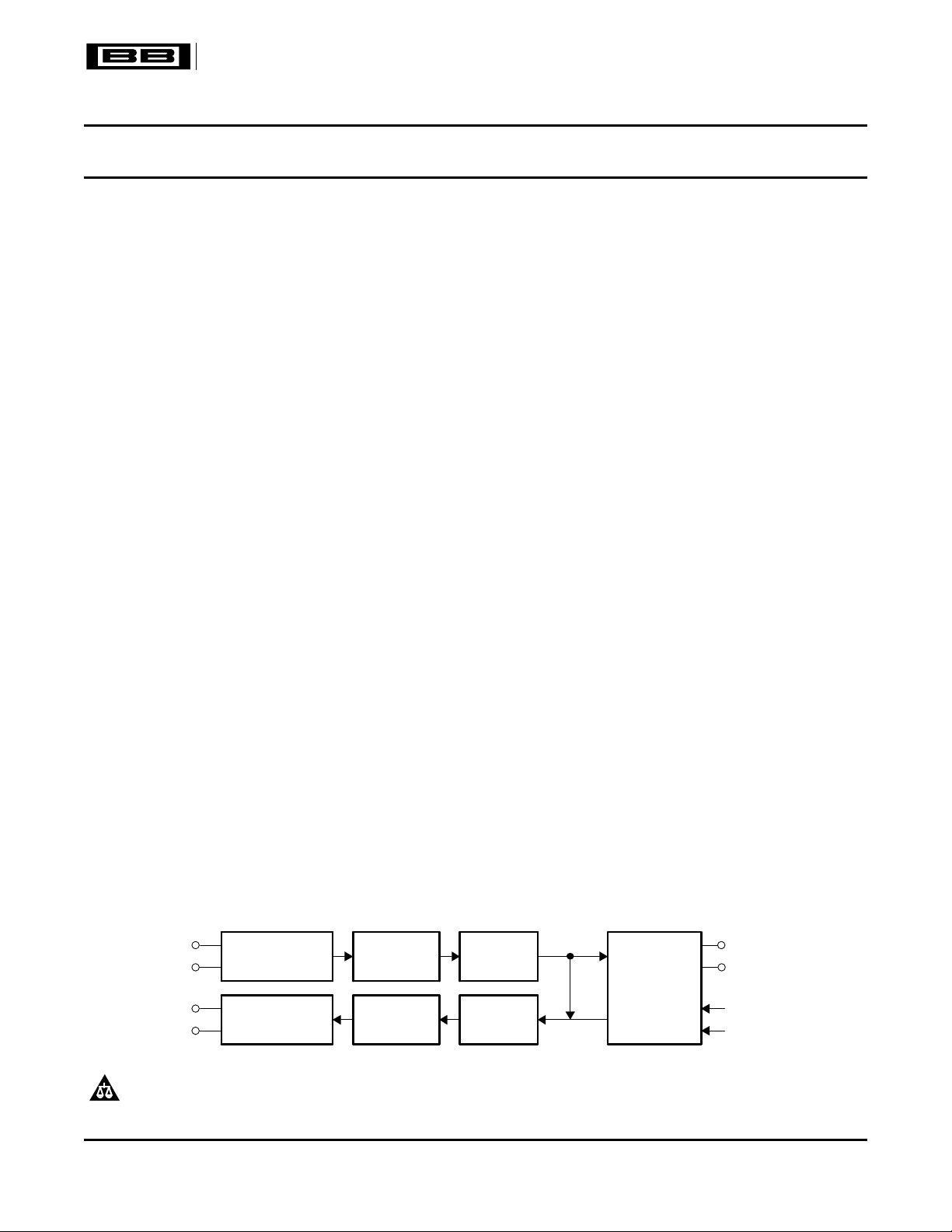
Lch In
Rch In
Analog Front-End
Delta-Sigma
Modulator
Digital
Decimation
Filter
Serial Interface
and
Mode Control
Digital Out
Mode Control
System Clock
B0006-03
Digital In
Digital
Interpolation
Filter
Lch Out
Rch Out
Low-Pass Filter
and
Output Buffer
Multilevel
Delta-Sigma
Modulator
18-BIT STEREO AUDIO CODEC, SINGLE-ENDED ANALOG INPUT/OUTPUT
PCM3000
PCM3001
SBAS055A – OCTOBER 2000 – REVISED OCTOBER 2004
FEATURES
• Monolithic 18-Bit ∆ Σ ADC and DAC
• Single 5-V Power Supply
• Small Package: SSOP-28
• 16- or 18-Bit Input/Output Data
• Accepts Seven Alternate Formats
• Stereo ADC:
– Single-Ended Voltage Input
– 64 × Oversampling Digital Filter
• Pass-Band Ripple: ± 0.05 dB
• Stop-Band Attenuation: –65 dB
– High Performance:
• THD+N: –88 dB
APPLICATIONS
• Sampling Keyboards
• Digital Mixers
• Mini-Disk Recorders
• Hard-Disk Recorders
• Karaoke Systems
• DSP-Based Car Stereo
• DAT Recorders
• Video Conferencing
• SNR: 94 dB
• Dynamic Range: 94 dB
DESCRIPTION
– Digital High-Pass Filter The PCM3000/3001 is a low-cost, single-chip stereo
• Stereo DAC
– Single-Ended Voltage Outut
– Analog Low-Pass Filter
– 8 × Oversampling Digital Filter
audio codec (analog-to-digital and digital-to-analog
converter) with single-ended analog voltage input and
output.
Both ADCs and DACs employ delta-sigma modulation with 64-times oversampling. The ADCs include
• Pass-Band Ripple: ± 0.17 dB a digital decimation filter and the DACs include an
• Stop-Band Attenuation: 35 dB
– High Performance:
• THD+N: –90 dB
• SNR: 98 dB
• Dynamic Range: 97 dB
• Special Features (PCM3000)
– Digital De-Emphasis
– Digital Attenuation (256 Steps)
– Soft Mute
8-times oversampling digital interpolation filter. The
DACs also include digital attenuation, de-emphasis,
infinite zero detection and soft mute to form a
complete subsystem. The PCM3000/3001 operates
with left-justified, right-justified, I2S or DSP data
formats.
The PCM3000 can be programmed with a three-wire
serial interface for special features and data formats.
The PCM3001 can be pin-programmed for data
formats.
The PCM3000 and PCM3001 are fabricated using a
– Digital Loopback highly advanced CMOS process and are available in
• Sample Rate: 4 kHz to 48 kHz
• System Clock: 256 fs, 384 fs, 512 f
s
a small 28-pin SSOP package. The PCM3000/3001
are suitable for a wide variety of cost-sensitive
consumer applications where good performance is
required.
Please be aware that an important notice concerning availability, standard warranty, and use in critical applications of Texas
Instruments semiconductor products and disclaimers thereto appears at the end of this data sheet.
System Two, Audio Precision are trademarks of Audio Precision, Inc.
All other trademarks are the property of their respective owners.
PRODUCTION DATA information is current as of publication date.
Products conform to specifications per the terms of the Texas
Instruments standard warranty. Production processing does not
necessarily include testing of all parameters.
Copyright © 2000–2004, Texas Instruments Incorporated
www.ti.com
PCM3000
PCM3001
SBAS055A – OCTOBER 2000 – REVISED OCTOBER 2004
This integrated circuit can be damaged by ESD. Texas Instruments recommends that all integrated
circuits be handled with appropriate precautions. Failure to observe proper handling and installation
procedures can cause damage.
ESD damage can range from subtle performance degradation to complete device failure. Precision
integrated circuits may be more susceptible to damage because very small parametric changes could
cause the device not to meet its published specifications.
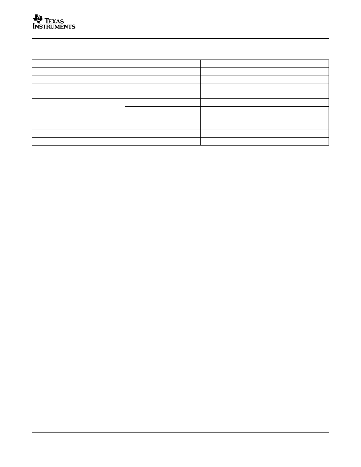
ELECTRICAL CHARACTERISTICS
All specifications at TA= 25 ° C, V
otherwise noted
PARAMETER TEST CONDITIONS MIN TYP MAX UNIT
DIGITAL INPUT/OUTPUT
Input Logic
(1)
V
IH
(1)
V
IL
(2)
I
IN
(3)
I
IN
(4)
V
IH
(4)
V
IL
(4)
I
IN
Output Logic
(5)
V
OH
(5)
V
OL
(6)
V
OH
(6)
V
OL
Clock Frequency
f
S
ADC CHARACTERISTICS
Resolution 18 Bits
DC Accuracy
(1) Pins 16, 17, 18, 22, 25, 26, 27, 28: LRCIN, BCKIN, DIN, CLKIO, MC/FMT2, MD/FMT1, ML/FMT0, RSTB
(2) Pins 16, 17, 18, 22: LRCIN, BCKIN, DIN, CLKIO (Schmitt-trigger input)
(3) Pins 25, 26, 27, 28: MC/FMT2, MD/FMT1, ML/FMT0, RSTB (Schmitt-trigger input, 70-k Ω internal pullup resistor)
(4) Pin 20: XTI
(5) Pins 19, 22: DOUT, CLKIO
(6) Pin 21: XTO
(7) Refer to Application Bulletin SBAA033 for information relating to operation at lower sampling frequencies.
(8) High-pass filter disabled (PCM3000 only) to measure dc offset
Input logic level VDC
Input logic current µ A
Input logic level
Input logic current ± 40 µ A
Output logic level
Output logic level
Sampling frequency 4
System clock frequency 384 f
Gain mismatch, channel-to-channel ± 1 ± 5
Gain error ± 2 ± 5
Gain drift ± 20 ppm of FSR/ ° C
Bipolar zero error High-pass filter off
Bipolar zero drift High-pass filter off
= V
DD
= 5 V, fS= 44.1 kHz, SYSCLK = 384 fS,CLKIO input, and 18-bit data, unless
CC
2
0.8
± 1
–120
0.64 V
DD
0.28 V
DD
I
= –1.6 mA 4.5
OUT
I
= 3.2 mA 0.5
OUT
I
= –3.2 mA 4.5
OUT
I
= 3.2 mA 0.5
OUT
256 f
512 f
(7)
S
S
S
(8)
(8)
1.024 11.2896 12.288
1.536 16.9344 18.432 MHz
2.048 22.5792 24.576
44.1 48 kHz
± 1.7 % of FSR
± 20 ppm of FSR/ ° C
VDC
VDC
% of FSR
2
www.ti.com
SBAS055A – OCTOBER 2000 – REVISED OCTOBER 2004
ELECTRICAL CHARACTERISTICS (continued)
All specifications at TA= 25 ° C, V
otherwise noted
PARAMETER TEST CONDITIONS MIN TYP MAX UNIT
Dynamic Performance
THD+N dB
Dynamic range f = 1 kHz, A-weighted 90 94 dB
Signal-to-noise ratio f = 1 kHz, A-weighted 90 94 dB
Channel separation 88 92 dB
Digital Filter Performance
Pass band 0.454 f
Stop band 0.583 f
Pass-band ripple ± 0.05 dB
Stop-band attenuation –65 dB
Delay time (latency) 17.4/f
Digital High-Pass Filter Response
Cutoff frequency –3 dB 0.019 f
ANALOG INPUT
Voltage range 0 dB (full scale) 2.9 Vp-p
Center voltage 2.1 VDC
Input impedance 15 k Ω
Antialiasing Filter
Cutoff frequency –3 dB, C
DAC CHARACTERISTICS
Resolution 18 Bits
DC Accuracy
Gain mismatch, channel-to-channel ± 1 ± 5 % of FSR
Gain error ± 1 ± 5 % of FSR
Gain drift ± 20 ppm of FSR/ ° C
Bipolar zero error ± 1 % of FSR
Bipolar zero drift ± 20 ppm of FSR/ ° C
Dynamic Performance
THD+N dB
Dynamic range EIAJ A-weighted 90 97 dB
Signal-to-noise ratio (idle channel) EIAJ A-weighted 92 98 dB
Channel separation 90 95 dB
Digital Filter Performance
Pass band 0.445 f
Stop band 0.555 f
Pass-band ripple ± 0.17 dB
Stop-band attenuation –35 dB
Delay time 11.1/f
(9)
(9)
= V
DD
= 5 V, fS= 44.1 kHz, SYSCLK = 384 fS,CLKIO input, and 18-bit data, unless
CC
f = 1 kHz, VIN= –0.5 dB –88 –80
f = 1 kHz, VIN= –60 dB –31
S
S
S
S
= 470 pF 170 kHz
EXT
V
= 0 dB (full scale) –90 –80
OUT
V
= –60 dB –34
OUT
S
S
S
PCM3000
PCM3001
Hz
Hz
s
mHz
Hz
Hz
s
(9) fIN= 1 kHz, using the System Two™ audio measurement system by Audio Precision™, rms mode with 20-kHz LPF, 400-Hz HPF
used for performance calculation or measurement.
3
www.ti.com
PCM3000
PCM3001
SBAS055A – OCTOBER 2000 – REVISED OCTOBER 2004
ELECTRICAL CHARACTERISTICS (continued)
All specifications at TA= 25 ° C, V
otherwise noted
PARAMETER TEST CONDITIONS MIN TYP MAX UNIT
Analog Output
Voltage range 0.62 V
Center voltage 0.5 V
Load impedance AC load 5 k Ω
Analog Low-Pass Filter
Frequency response f = 20 kHz –0.16 dB
POWER SUPPLY REQUIREMENTS
V
CC
V
DD
ICC, I
DD
TEMPERATURE RANGE
T
A
T
stg
θ
JA
Voltage range
(10)
Supply current V
Power dissipation V
Operation –25 85 ° C
Storage –55 125 ° C
Thermal resistance 100 ° C/W
= V
DD
= 5 V, fS= 44.1 kHz, SYSCLK = 384 fS,CLKIO input, and 18-bit data, unless
CC
CC
CC
4.5 5 5.5 VDC
4.5 5 5.5 VDC
= V
CC
CC
= 5 V 32 50 mA
DD
= V
= 5 V 160 250 mW
DD
Vp-p
VDC
(10) With no load on XTO and CLKIO
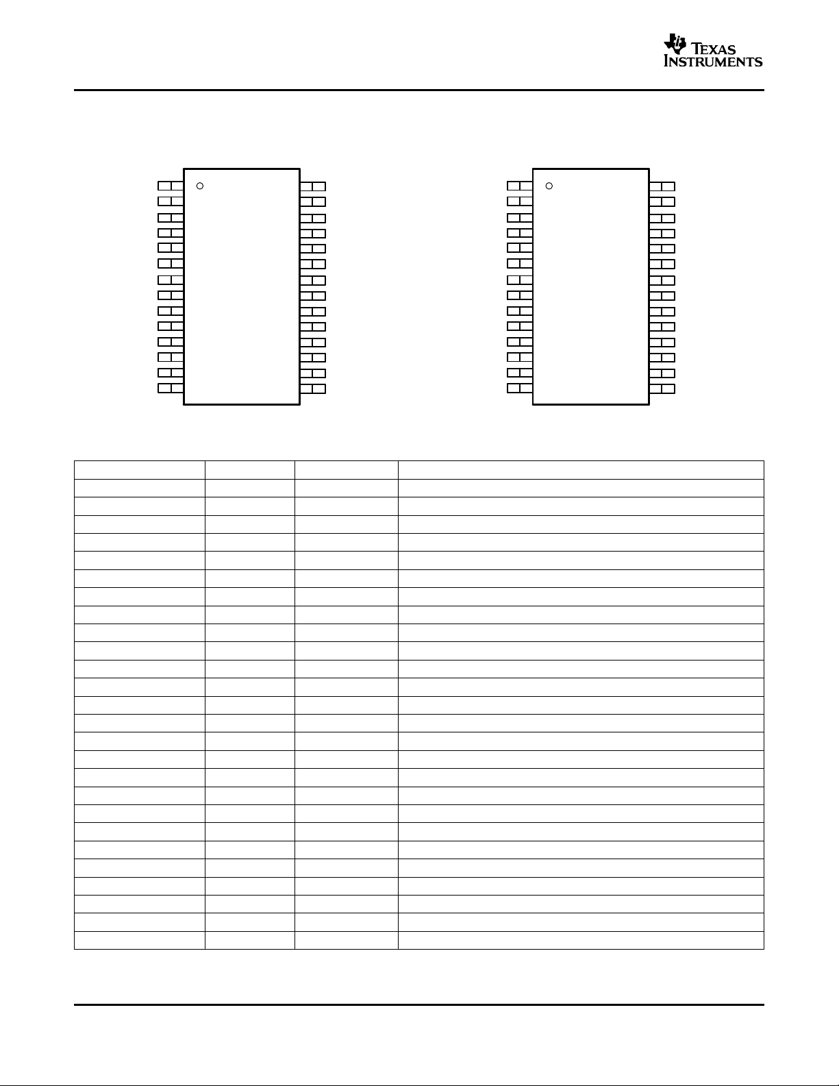
PACKAGE/ORDERING INFORMATION
PRODUCT PACKAGE QUANTITY
PCM3000E PCM3000E
28-pin SSOP DB
PCM3001E PCM3001E
PACKAGE PACKAGE ORDERING TRANSPORT
CODE MARKING NUMBER MEDIA
PCM3000E Rails 47
PCM3000E/2K Tape and reel 2000
PCM3001E Rails 47
PCM3001E/2K Tape and reel 2000
ABSOLUTE MAXIMUM RATINGS
over operating free-air temperature range (unless otherwise noted)
Supply voltage: VDD, VCC1, VCC2 –0.3 V to 6.5 V
Supply voltage differences ± 0.1 V
GND voltage differences ± 0.1 V
Digital input voltage –0.3 to V
Analog input voltage –0.3 to VCC1, VCC2 + 0.3 V, < 6.5 V
Power dissipation 300 mW
Input current (any pins except supplies) ± 10 mA
Operating temperature –25 ° C to 85 ° C
Storage temperature –55 ° C to 125 ° C
Lead temperature, soldering 260 ° C, 5 s
Package temperature (IR reflow, peak) 235 ° C
+ 0.3 V, < 6.5 V
DD
4
www.ti.com
SBAS055A – OCTOBER 2000 – REVISED OCTOBER 2004
RECOMMENDED OPERATING CONDITIONS
over operating free-air temperature range (unless otherwise noted)
MIN NOM MAX UNIT
Analog supply voltage, VCC1, VCC2 4.5 5 5.5 VDC
Digital supply voltage, V
Analog input voltage, full scale (–0 dB) 2.9 Vp-p
Digital input logic family TTL
Digital input clock frequency
Analog output load resistance 5 k Ω
Analog output load capacitance 50 pF
Digital output load capacitance 10 pF
Operating free-air temperature, T
DD
System clock 8.192 24.576 MHz
Sampling clock 32 48 kHz
A
4.5 5 5.5 VDC
–25 85 ° C
PCM3000
PCM3001
5
www.ti.com
1
2
3
4
5
6
7
8
9
10
11
12
13
14
28
27
26
25
24
23
22
21
20
19
18
17
16
15
VINL
VCC1
AGND1
V
REF
L
V
REF
R
VINR
CINPR
CINNR
CINNL
CINPL
VCOM
V
OUT
R
AGND2
VCC2
RSTB
ML
MD
MC
DGND
V
DD
CLKIO
XTO
XTI
DOUT
DIN
BCKIN
LRCIN
V
OUT
L
PCM3000
(TOP VIEW)
P0007-01
1
2
3
4
5
6
7
8
9
10
11
12
13
14
28
27
26
25
24
23
22
21
20
19
18
17
16
15
VINL
VCC1
AGND1
V
REF
L
V
REF
R
VINR
CINPR
CINNR
CINNL
CINPL
VCOM
V
OUT
R
AGND2
VCC2
RSTB
FMT0
FMT1
FMT2
DGND
V
DD
CLKIO
XTO
XTI
DOUT
DIN
BCKIN
LRCIN
V
OUT
L
PCM3001
(TOP VIEW)
PCM3000
PCM3001
SBAS055A – OCTOBER 2000 – REVISED OCTOBER 2004
PIN CONFIGURATION—PCM3000/3001
NAME PIN I/O DESCRIPTION
AGND1 3 – ADC analog ground
AGND2 13 – DAC analog ground
BCKIN 17 I Bit clock input
CINNL 9 – ADC antialias filter capacitor (–), Lch
CINNR 8 – ADC antialias filter capacitor (–), Rch
CINPL 10 – ADC antialias filter capacitor (+), Lch
CINPR 7 – ADC antialias filter capacitor (+), Rch
CLKIO 22 I/O Buffered oscillator output or external clock input
DGND 24 – Digital ground
DIN 18 I Data input
DOUT 19 O Data output
LRCIN 16 I Sample rate clock input (fS)
MC 25 I Serial mode control, bit clock
MD 26 I Serial mode control, data
ML 27 I Serial mode control, strobe pulse
RSTB 28 I Reset, active-low
V
CC
V
CC
V
DD
VCOM 11 – DAC output common
(1) Schmitt-trigger input
(2) With 70-k Ω typical internal pullup resistor
6
VINL 1 I ADC analog input, Lch
VINR 6 I ADC analog input, Rch
V
OUT
V
OUT
V
REF
V
REF
PIN ASSIGNMENTS—PCM3000
(1)
(1)
1 2 – ADC analog power supply
2 14 – DAC analog power supply
23 – Digital power supply
L 15 O DAC analog output, Lch
R 12 O DAC analog output, Rch
L 4 – ADC input reference, Lch
R 5 – ADC input reference, Rch
(1)
(1)
(1) (2)
www.ti.com
NAME PIN I/O DESCRIPTION
XTI 20 I Oscillator input
XTO 21 O Oscillator output
NAME PIN I/O DESCRIPTION
AGND1 3 – ADC analog ground
AGND2 13 – DAC analog ground
BCKIN 17 I Bit clock input
CINNL 9 – ADC antialias filter capacitor (–), Lch
CINNR 8 – ADC antialias filter capacitor (–), Rch
CINPL 10 – ADC antialias filter capacitor (+), Lch
CINPR 7 – ADC antialias filter capacitor (+), Rch
CLKIO 22 I/O Buffered oscillator output or external clock input
DGND 24 – Digital ground
DIN 18 I Data input
DOUT 19 O Data output
FMT0 27 I Audio data format control 0
FMT1 26 I Audio data format control 1
FMT2 25 I Audio data format control 2
LRCIN 16 I Sample rate clock input (fS)
RSTB 28 I Reset, active-low
V
1 2 – ADC analog power supply
CC
V
2 14 – DAC analog power supply
CC
V
DD
VCOM 11 – DAC output common
VINL 1 I ADC analog input, Lch
VINR 6 I ADC analog input, Rch
V
L 15 O DAC analog output, Lch
OUT
V
R 12 O DAC analog output, Rch
OUT
V
L 4 – ADC input reference, Lch
REF
V
R 5 – ADC input reference, Rch
REF
XTI 20 I Oscillator input
XTO 21 O Oscillator output
(1) Schmitt-trigger input
(2) With 70-k Ω typical internal pullup resistor
PCM3000
PCM3001
SBAS055A – OCTOBER 2000 – REVISED OCTOBER 2004
PIN ASSIGNMENTS—PCM3000 (continued)
PIN ASSIGNMENTS—PCM3001
(1)
(1)
(1)
(1) (2)
(1) (2)
(1) (2)
(1)
(1) (2)
23 – Digital power supply
7
www.ti.com
0.002
0.004
0.006
0.008
0.010
−25 0 25 50 75 100
TA − Free-Air Temperature − °C
THD+N − Total Harm. Dist. + Noise at FS − %
FS
4
3
2
0
1
−60 dB
G001
THD+N − Total Harm. Dist. + Noise at −60 dB − %
0.002
0.004
0.006
0.008
0.010
4.25 4.50 4.75 5.00 5.25 5.50 5.75
VCC − Supply Voltage − V
THD+N − Total Harm. Dist. + Noise at FS − %
4
3
2
0
1
THD+N − Total Harm. Dist. + Noise at −60 dB − %
G002
−60 dB
FS
90
92
94
96
98
4.25 4.50 4.75 5.00 5.25 5.50 5.75
VCC − Supply Voltage − V
Dynamic Range − dB
98
96
94
90
92
SNR − Signal-to-Noise Ratio − dB
G004
Dynamic Range
SNR
0.002
0.004
0.006
0.008
0.010
System Clock
THD+N − Total Harm. Dist. + Noise at FS − %
4
3
2
0
1
G003
THD+N − Total Harm. Dist. + Noise at −60 dB − %
512 f
S
256 f
S
384 f
S
44.1 kHz
FS
−60 dB
48 kHz
48 kHz
44.1 kHz
PCM3000
PCM3001
SBAS055A – OCTOBER 2000 – REVISED OCTOBER 2004
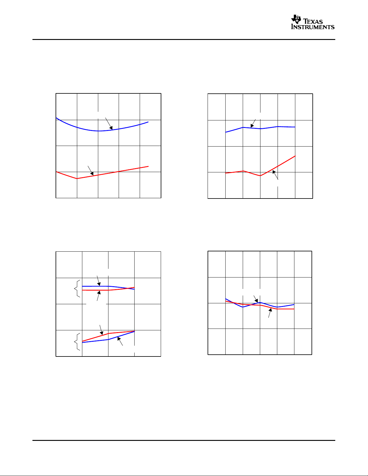
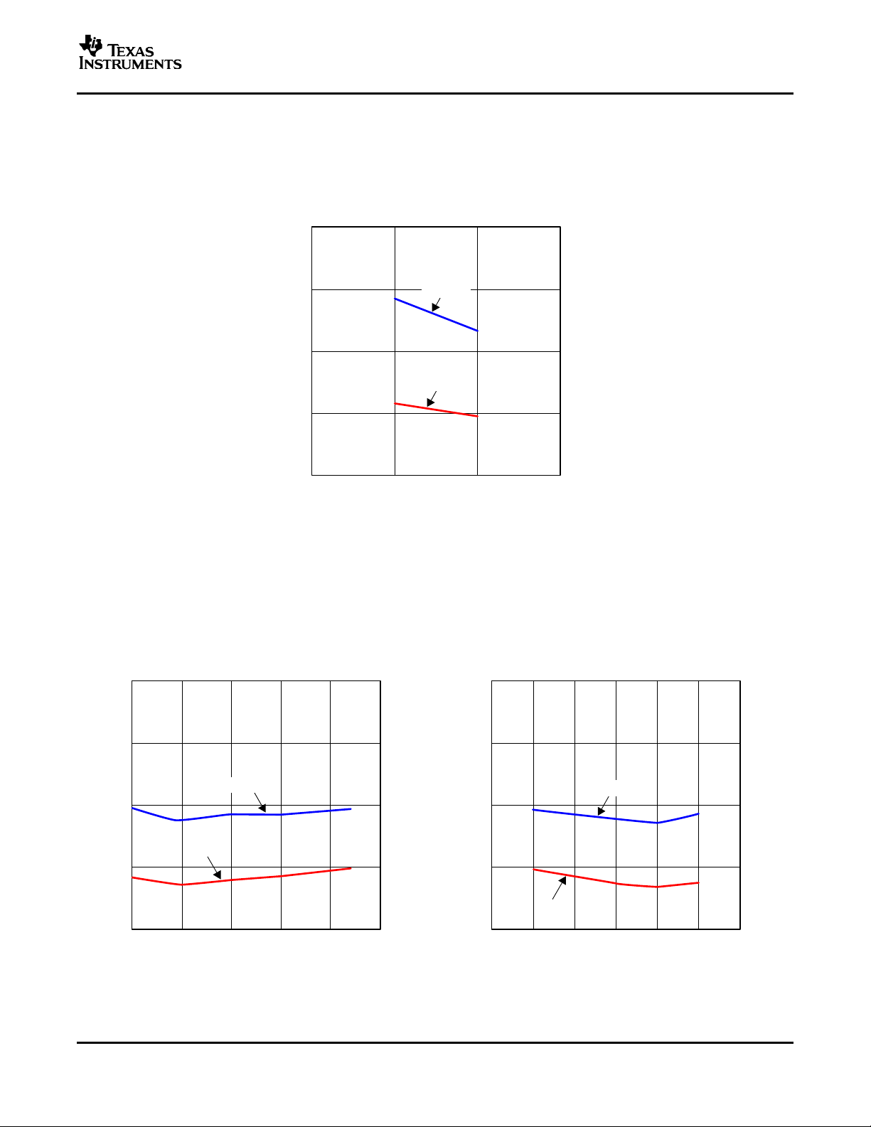
TYPICAL PERFORMANCE CURVES OF ADC SECTION
All specifications at TA= 25 ° C, V
TEMPERATURE POWER SUPPLY
= V
CC
THD+N THD+N
vs vs
= 5 V, fIN= 1 kHz, fS= 44.1 kHz, 18-bit data, V
DD
unless otherwise noted
= 2.9 Vp-p, and SYSCLK = 384 fS,
IN
Figure 1. Figure 2.
THD+N SNR AND DYNAMIC RANGE
vs vs
SYSTEM CLOCK AND SAMPLING FREQUENCY POWER SUPPLY
Figure 3. Figure 4.
8
www.ti.com
0.002
0.004
0.006
0.008
0.010
Resolution
THD+N − Total Harm. Dist. + Noise at FS − %
4
3
2
0
1
G005
THD+N − Total Harm. Dist. + Noise at −60 dB − %
−60 dB
18-Bit16-Bit
FS
0.002
0.004
0.006
0.008
0.010
−25 0 25 50 75 100
TA − Free-Air Temperature − °C
THD+N − Total Harm. Dist. + Noise at FS − %
FS
4
3
2
0
1
G006
THD+N − Total Harm. Dist. + Noise at −60 dB − %
−60 dB
0.002
0.004
0.006
0.008
0.010
4.25 4.50 4.75 5.00 5.25 5.50 5.75
VCC − Supply Voltage − V
THD+N − Total Harm. Dist. + Noise at FS − %
4
3
2
0
1
THD+N − Total Harm. Dist. + Noise at −60 dB − %
G007
−60 dB
FS
TYPICAL PERFORMANCE CURVES OF ADC SECTION (continued)
All specifications at TA= 25 ° C, V
unless otherwise noted
= V
CC
= 5 V, fIN= 1 kHz, fS= 44.1 kHz, 18-bit data, V
DD
OUTPUT DATA RESOLUTION
PCM3000
PCM3001
SBAS055A – OCTOBER 2000 – REVISED OCTOBER 2004
= 2.9 Vp-p, and SYSCLK = 384 fS,
IN
THD+N
vs
TYPICAL PERFORMANCE CURVES OF DAC SECTION
All specifications at TA= 25 ° C, V
THD+N THD+N
TEMPERATURE POWER SUPPLY
Figure 5.
= V
CC
= 5 V, fIN= 1 kHz, fS= 44.1 kHz, 18-bit data, and SYSCLK = 384 fS, unless
DD
otherwise noted
vs vs
Figure 6. Figure 7.
9
www.ti.com
92
94
96
98
100
4.25 4.50 4.75 5.00 5.25 5.50 5.75
VCC − Supply Voltage − V
Dynamic Range − dB
100
98
96
92
94
SNR − Signal-to-Noise Ratio − dB
G009
Dynamic Range
SNR
0.002
0.004
0.006
0.008
0.010
System Clock
THD+N − Total Harm. Dist. + Noise at FS − %
4
3
2
0
1
G008
THD+N − Total Harm. Dist. + Noise at −60 dB − %
512 f
S
256 f
S
384 f
S
FS
−60 dB
48 kHz
48 kHz
44.1 kHz
44.1 kHz
0.002
0.004
0.006
0.008
0.010
Resolution
THD+N − Total Harm. Dist. + Noise at FS − %
4
3
2
0
1
G010
THD+N − Total Harm. Dist. + Noise at −60 dB − %
−60 dB
18-Bit16-Bit
FS
PCM3000
PCM3001
SBAS055A – OCTOBER 2000 – REVISED OCTOBER 2004
TYPICAL PERFORMANCE CURVES OF DAC SECTION (continued)
All specifications at TA= 25 ° C, V
otherwise noted
SYSTEM CLOCK AND SAMPLING FREQUENCY POWER SUPPLY
= V
CC
= 5 V, fIN= 1 kHz, fS= 44.1 kHz, 18-bit data, and SYSCLK = 384 fS, unless
DD
THD+N SNR AND DYNAMIC RANGE
vs vs
Figure 8. Figure 9.
THD+N
vs
INPUT DATA RESOLUTION
Figure 10.
10
www.ti.com
DECIMATION FILTER
Normalized Frequency [× fS Hz]
−200
−150
−100
−50
0
0 8 16 24 32
Amplitude − dB
G011
Normalized Frequency [× fS Hz]
−100
−80
−60
−40
−20
0
0.0 0.2 0.4 0.6 0.8 1.0
Amplitude − dB
G012
Normalized Frequency [× fS Hz]
−1.0
−0.8
−0.6
−0.4
−0.2
0.0
0.2
0.0 0.1 0.2 0.3 0.4 0.5
Amplitude − dB
G013
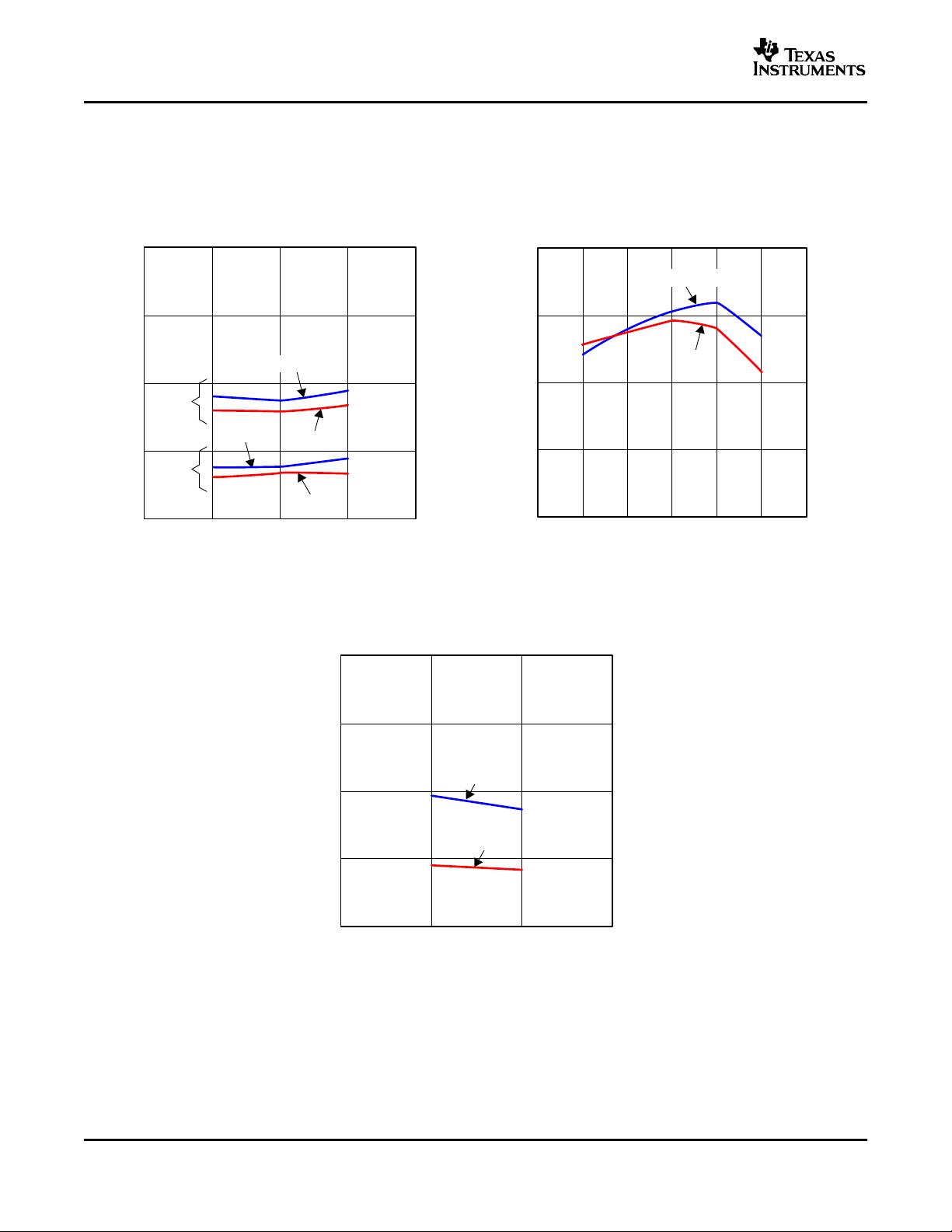
TYPICAL PERFORMANCE CURVES OF INTERNAL FILTERS (ADCs)
All specifications at TA= 25 ° C, V
OVERALL CHARACTERISTICS STOP-BAND ATTENUATION CHARACTERISTICS
= V
CC
= 5 V, and SYSCLK = 384 fS, unless otherwise noted
DD
PCM3000
PCM3001
SBAS055A – OCTOBER 2000 – REVISED OCTOBER 2004
Figure 11. Figure 12.
PASS-BAND RIPPLE CHARACTERISTICS
Figure 13.
11
www.ti.com
Normalized Frequency [× fS/1000 Hz]
−1.0
−0.8
−0.6
−0.4
−0.2
0.0
0.2
0 1 2 3 4
Amplitude − dB
G014
−1.0
−0.8
−0.6
−0.4
−0.2
0.0
0.2
f − Frequency − Hz
Amplitude − dB
1 10 100 100k1k 10k
G015
470 pF
1000 pF
−50
−40
−30
−20
−10
0
f − Frequency − Hz
Amplitude − dB
1 10 100 10M1k 10k
G016
100k 1M
470 pF
1000 pF
PCM3000
PCM3001
SBAS055A – OCTOBER 2000 – REVISED OCTOBER 2004
TYPICAL PERFORMANCE CURVES OF INTERNAL FILTERS (ADCs) (continued)
All specifications at TA= 25 ° C, V
HIGH-PASS FILTER
= V
CC
= 5 V, and SYSCLK = 384 fS, unless otherwise noted
DD
HIGH-PASS FILTER RESPONSE
ANTIALIASING FILTER
Figure 14.
ANTIALIASING FILTER PASS-BAND ANTIALIASING FILTER OVERALL
FREQUENCY RESPONSE (C
= 470 pF, 1000 pF) FREQUENCY RESPONSE (C
EXT
= 470 pF, 1000 pF)
EXT
12
Figure 15. Figure 16.

www.ti.com
DIGITAL FILTER
−100
−80
−60
−40
−20
0
Level − dB
f − Frequency − Hz
0.4536 f
S
G017
0
1.3605 fS2.2675 f
S
4.0815 f
S
3.1745 f
S
−1.0
−0.8
−0.6
−0.4
−0.2
0.0
Level − dB
f − Frequency − Hz
0.1134 f
S
G018
0 0.2268 fS0.3402 fS0.4535 f
S
−12
−10
−8
−6
−4
−2
0
Level − dB
f − Frequency − Hz
5k
G019
0 25k10k 15k 20k
−0.6
−0.4
−0.2
0.0
0.2
0.4
0.6
Error − dB
f − Frequency − Hz
3628
G020
0 145127256 10884
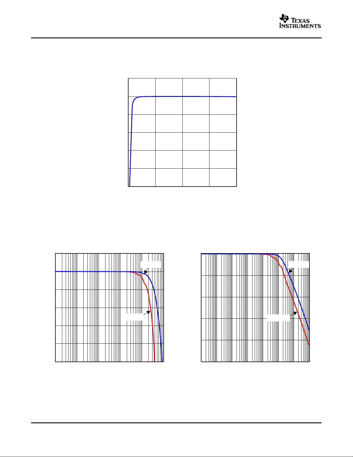
TYPICAL PERFORMANCE CURVES OF INTERNAL FILTERS (DACs)
All specifications at TA= 25 ° C, V
OVERALL FREQUENCY CHARACTERISTIC PASS-BAND RIPPLE CHARACTERISTIC
= V
CC
= 5 V, and SYSCLK = 384 fS, unless otherwise noted
DD
PCM3000
PCM3001
SBAS055A – OCTOBER 2000 – REVISED OCTOBER 2004
DE-EMPHASIS FILTER
DE-EMPHASIS FREQUENCY RESPONSE (32 kHz) DE-EMPHASIS ERROR (32 kHz)
13

www.ti.com
−12
−10
−8
−6
−4
−2
0
Level − dB
f − Frequency − Hz
5k
G021
0 25k10k 15k 20k
−0.6
−0.4
−0.2
0.0
0.2
0.4
0.6
Error − dB
f − Frequency − Hz
4999.8375
G022
0 19999.359999.675 14999.5125
−12
−10
−8
−6
−4
−2
0
Level − dB
f − Frequency − Hz
5k
G023
0 25k10k 15k 20k
−0.6
−0.4
−0.2
0.0
0.2
0.4
0.6
Error − dB
f − Frequency − Hz
5442
G024
0 2176810884 16326
PCM3000
PCM3001
SBAS055A – OCTOBER 2000 – REVISED OCTOBER 2004
TYPICAL PERFORMANCE CURVES OF INTERNAL FILTERS (DACs) (continued)
All specifications at TA= 25 ° C, V
DE-EMPHASIS FREQUENCY RESPONSE (44.1 kHz) DE-EMPHASIS ERROR (44.1 kHz)
= V
CC
= 5 V, and SYSCLK = 384 fS, unless otherwise noted
DD
DE-EMPHASIS FREQUENCY RESPONSE (48 kHz) DE-EMPHASIS ERROR (48 kHz)
14

www.ti.com
−60
−55
−50
−45
−40
−35
−30
−25
−20
−15
−10
−5
0
5
10
f − Frequency − Hz
Level − dB
10 100 10M1k 10k
G026
100k 1M
−1.0
−0.5
0.0
0.5
1.0
f − Frequency − Hz
Level − dB
20 100 24k1k 10k
G025
TYPICAL PERFORMANCE CURVES OF INTERNAL FILTERS (DACs) (continued)
All specifications at TA= 25 ° C, V
= V
CC
= 5 V, and SYSCLK = 384 fS, unless otherwise noted
DD
ANALOG LOW-PASS FILTER
PCM3000
PCM3001
SBAS055A – OCTOBER 2000 – REVISED OCTOBER 2004
INTERNAL ANALOG FILTER FREQUENCY RESPONSE INTERNAL ANALOG FILTER FREQUENCY RESPONSE
(20 Hz–24 kHz, EXPANDED SCALE) (10 Hz–10 MHz)
15

www.ti.com
MC(FMT2)
(1)
MD(FMT1)
(1)
Analog
Front-End
Circuit
LRCIN
VINL
Reference
V
REF
L
V
REF
R
VINR
Delta-Sigma
Modulator
Delta-Sigma
Modulator
Decimation
and
High-Pass Filter
Power Supply
Reset
Serial Data
Interface
DOUT
(+)
(−)
(−)
(+)
Mode
Control
Interface
Analog
Front-End
Circuit
Decimation
and
High-Pass Filter
ADC
BCKIN
DIN
Analog
Low-Pass
Filter
V
OUT
L
Multilevel
Delta-Sigma
Modulator
Interpolation
Filter
8× Oversampling
Analog
Low-Pass
Filter
V
OUT
R
Multilevel
Delta-Sigma
Modulator
Interpolation
Filter
8× Oversampling
DAC
ML(FMT0)
(1)
RSTB
Clock/OSC Manager
CLKIOAGND2 VCC2 AGND1 VCC1 DGND V
DD
B0004-05
CINNL
CINPL
CINNR
CINPR
VCOM
XTO XTI
Loop Control
PCM3000
PCM3001
SBAS055A – OCTOBER 2000 – REVISED OCTOBER 2004
Block Diagram
16

www.ti.com
15 kΩ
1 kΩ
470 pF
910
VINL
V
REF
L
CINPL CINNL
1
4
Delta-Sigma
Modulator
(+)
V
REF
+
2.2 µF
4.7 µF
+
+
−
(−)
+
−
1 kΩ
S0011-04
Figure 17. Analog Front-End (Single-Channel)
PCM3000
PCM3001
SBAS055A – OCTOBER 2000 – REVISED OCTOBER 2004
PCM AUDIO INTERFACE
The four-wire digital audio interface for the PCM3000/3001 is on LRCIN (pin 16), BCKIN (pin 17), DIN (pin 18),
and DOUT (pin 19). The PCM3000/3001 can operate with seven different data formats. For the PCM3000, these
formats are selected through program register 3 in the software mode. For the PCM3001, data formats are
selected by pin-strapping the three format pins. Figure 18 , Figure 19 , Figure 20 and Figure 21 illustrate the audio
data input/output format. Figure 22 shows the audio data input/output timing. The PCM3000/3001 can accept 32,
48, or 64 bit clocks (BCKIN) during one clock of LRCIN. Only formats 0, 2, and 6 can be selected when 32 bit
clocks/LRCIN are applied.
17

www.ti.com
DAC: 16-Bit, MSB-First, Right-Justified
FORMAT 0: FMT[2:0] = 000
LRCIN Right-ChannelLeft-Channel
BCKIN
DIN
MSB
LSB
MSB
LSB
321 16151416 321 161514
BCKIN
LRCIN
Right-ChannelLeft-Channel
DOUT 1
14 15 16321
MSB LSB MSB LSB
14 15 16321
ADC: 16-Bit, MSB-First, Left-Justified
LRCIN Right-ChannelLeft-Channel
BCKIN
DIN
MSB
LSB
MSB
LSB
16 17 18321 16 17 1832118
DAC: 18-Bit, MSB-First, Right-Justified
FORMAT 1: FMT[2:0] = 001
BCKIN
LRCIN
Right-ChannelLeft-Channel
DOUT 1
16 17 18321
MSB LSB MSB LSB
16 17 18321
ADC: 18-Bit, MSB-First, Left-Justified
T0016-07
PCM3000
PCM3001
SBAS055A – OCTOBER 2000 – REVISED OCTOBER 2004
Figure 18. Audio Data Input/Output Format (Formats 0 and 1)
18

www.ti.com
DAC: 16-Bit, MSB-First, Right-Justified
FORMAT 2: FMT[2:0] = 010
LRCIN Right-ChannelLeft-Channel
BCKIN
DIN
MSB
LSB
MSB
LSB
321 16151416 321 161514
ADC: 16-Bit, MSB-First, Right-Justified
LRCIN Right-ChannelLeft-Channel
BCKIN
DIN
MSB
LSB
MSB
LSB
16 17 18321 16 17 1832118
DAC: 18-Bit, MSB-First, Right-Justified
FORMAT 3: FMT[2:0] = 011
ADC: 18-Bit, MSB-First, Right-Justified
T0016-08
LRCIN
Right-ChannelLeft-Channel
BCKIN
DOUT
MSB
LSB
MSB
LSB
321 16151416 321 161514
LRCIN Right-ChannelLeft-Channel
BCKIN
DOUT
MSB
LSB
MSB
LSB
16 17 18321 16 17 1832118
PCM3000
PCM3001
SBAS055A – OCTOBER 2000 – REVISED OCTOBER 2004
Figure 19. Audio Data Input/Output Format (Formats 2 and 3)
19

www.ti.com
DAC: 18-Bit, MSB-First, Left-Justified
FORMAT 4: FMT[2:0] = 100
ADC: 18-Bit, MSB-First, Left-Justified
DAC: 18-Bit, MSB-First, I2S
FORMAT 5: FMT[2:0] = 101
T0016-09
BCKIN
LRCIN Right-ChannelLeft-Channel
DIN
1
16 17 18321
MSB LSB MSB LSB
16 17 18321
BCKIN
LRCIN
Right-ChannelLeft-Channel
DOUT 1
16 17 18321
MSB LSB MSB LSB
16 17 18321
LRCIN
Right-ChannelLeft-Channel
BCKIN
DIN
MSB LSB MSB LSB
16 17 18321 16 17 18321
LRCIN
Right-ChannelLeft-Channel
BCKIN
DOUT
MSB LSB MSB LSB
16 17 18321 16 17 18321
ADC: 18-Bit, MSB-First, I2S
PCM3000
PCM3001
SBAS055A – OCTOBER 2000 – REVISED OCTOBER 2004
Figure 20. Audio Data Input/Output Format (Formats 4 and 5)
20

www.ti.com
DAC: 16-Bit, MSB-First, DSP-Frame
FORMAT 6: FMT[2:0] = 110
LRCIN Right-ChannelLeft-Channel
BCKIN
DIN
MSB
LSB
MSB
LSB
321 16151416 321 161514
ADC: 16-Bit, MSB-First, DSP-Frame
T0016-10
1
LRCIN
Right-ChannelLeft-Channel
BCKIN
DOUT
MSB
LSB
MSB
LSB
321 16151416 321 161514 1
SBAS055A – OCTOBER 2000 – REVISED OCTOBER 2004
Figure 21. Audio Data Input/Output Format (Format 6)
PCM3000
PCM3001
21

www.ti.com
BCKIN
LRCIN
DIN
t
(BCH)
t
(BCL)
t
(LRP)
t
(LB)
t
(BCY)
1.4 V
t
(BL)
DOUT
t
(BDO)
t
(LDO)
0.5 V
DD
t
(DIS)
t
(DIH)
1.4 V
1.4 V
T0021−02
PCM3000
PCM3001
SBAS055A – OCTOBER 2000 – REVISED OCTOBER 2004
BCKIN pulse cycle time t
BCKIN pulse duration, HIGH t
BCKIN pulse duration, LOW t
BCKIN rising edge to LRCIN edge t
LRCIN edge to BCKIN rising edge t
LRCIN pulse duration t
DIN setup time t
DIN hold time t
DOUT delay time to BCKIN falling edge t
DOUT delay time to LRCIN edge t
Rising time of all signals t
Falling time of all signals t
300 ns (min)
(BCY)
120 ns (min)
(BCH)
120 ns (min)
(BCL)
40 ns (min)
(BL)
40 ns (min)
(LB)
t
(LRP)
(DIS)
(DIH)
(BDO)
(LDO)
(RISE)
(FALL)
(min)
(BCY)
40 ns (min)
40 ns (min)
40 ns (max)
40 ns (max)
20 ns (max)
20 ns (max
Figure 22. Audio Data Input/Output Timing
SYSTEM CLOCK
The system clock for the PCM3000/3001 must be either 256 fS, 384 fS, or 512 fS, where fSis the audio sampling
frequency. The system clock can be either a crystal oscillator placed between XTI (pin 20) and XTO (pin 21), or
an external clock input. If an external clock is used, the clock is provided to either XTI or CLKIO (pin 22), and
XTO is open. The PCM3000/3001 has an XTI clock detection circuit which senses if an XTI clock is operating.
When the external clock is delivered to XTI, CLKIO is a buffered output of XTI. When XTI is connected to
ground, the external clock must be tied to CLKIO. For best performance, the external-clock-input-2 circuit in
Figure 23 is recommended.
The PCM3000/3001 also has a system-clock detection circuit which automatically senses if the system clock is
operating at 256 fS, 384 fS, or 512 fS. When a 384-f
256 fSautomatically. The 256-f
clock is used to operate the digital filters and the modulators.
S
Table 1 lists the relationship of typical sampling frequencies and system clock frequencies, and Figure 23 and
Figure 24 illustrate the typical system clock connections and external system clock timing.
or 512-f
S
system clock is used, the clock is divided into
S
22

www.ti.com
CLKIO
Clock Divider
S0017−01
R
256-fS Internal System Clock
PCM3000/3001
XTI
XTO
Xtal
C
1
C
2
Crystal Resonator Connection (Xtal must be fundamental mode, parallel resonant)
CLKIO
Clock Divider
R
256-fS Internal System Clock
PCM3000/3001
XTI
XTO
External Clock
(CMOS I/F)
External Clock Input 1 : (XTO is open)
CLKIO
Clock Divider
R
256-fS Internal System Clock
PCM3000/3001
XTI
XTO
External Clock Input 2 : (XTO is open)
External Clock
(TTL I/F)
C1 = C2 = 10 to 33 pF
PCM3000
PCM3001
SBAS055A – OCTOBER 2000 – REVISED OCTOBER 2004
Figure 23. System Clock Connections
23

www.ti.com
t
(CLKIH)
XTI or CLKIO
1.4 V
3.2 V
t
(CLKIL)
T0005-06
XTI
0.8 V
2.0 V
CLKIO
1024 System Clock Periods
Reset Reset Removal
4.4 V
4.0 V
3.6 V
V
DD
Internal Reset
System Clock
(XTI or CLKIO)
T0014-04
3 Clocks Minimum
PCM3000
PCM3001
SBAS055A – OCTOBER 2000 – REVISED OCTOBER 2004
SAMPLING RATE FREQUENCY (kHz) SYSTEM CLOCK FREQUENCY (MHz)
32 8.1920 12.2880 16.3840
44.1 11.2896 16.9344 22.5792
48 12.2880 18.4320 24.5760
Table 1. System Clock Frequencies
256 f
S
384 f
S
512 f
S
System clock pulse duration, HIGH t
System clock pulse duration, LOW t
(CLKIH)
(CLKIL)
12 ns (min)
12 ns (min)
Figure 24. External System Clock Timing
POWER-ON RESET
The PCM3000/3001 has internal power-on reset circuitry. Power-on reset occurs when the system clock (XTI or
CLKIO) is active and V
cycles prior to V
DD
> 4 V. For the PCM3001, the system clock must complete a minimum of 3 complete
DD
> 4 V to ensure proper reset operation. The initialization sequence requires 1024 system
cycles for completion, as shown in Figure 25 . Figure 26 shows the state of the DAC and ADC outputs during and
after the reset sequence.
24
Figure 25. Internal Power-On Reset Timing

www.ti.com
T0019-03
Reset
Internal Reset
DAC V
OUT
32/f
S
Reset Removal or Power Down
(1)
Off
ADC DOUT
Zero Data Normal Data
(2)
VCOM
(0.5 VCC2)
4096/f
S
Zero Data
Ready/Operation
t
(RST)
Reset Removal
1024 System Clock Periods
RSTB
Internal Reset
System Clock
(XTI or CLKIO)
t
(RST)
= 40 ns (min)
Reset
T0015-04
RSTB Pulse Duration
SBAS055A – OCTOBER 2000 – REVISED OCTOBER 2004
(1) Power down is for PCM3000 only.
(2) The HPF transient response (exponentially attenuated signal from ± 1.5% dc with 200-ms time constant) appears
initially.
Figure 26. DAC Output and ADC Output for Reset and Power Down
PCM3000
PCM3001
EXTERNAL RESET
The PCM3000/3001 includes a reset input, RSTB (pin 28). As shown in Figure 27 , the external reset signal must
drive RSTB low for a minimum of 40 nanoseconds while the system clock is active in order to initiate the reset
sequence. Initialization starts on the rising edge of RSTB, and requires 1024 system clock cycles for completion.
Figure 26 shows the state of the DAC and ADC outputs during and after the reset sequence.
Figure 27. External Forced-Reset Timing
SYNCHRONIZATION WITH THE DIGITAL AUDIO SYSTEM
The PCM3000/3001 operates with LRCIN synchronized to the system clock. The codec does not require any
specific phase relationship between LRCIN and the system clock, but there must be synchronization of LRCIN
and the system clock. If the synchronization between the system clock and LRCIN changes more than 6 bit
clocks (BCKIN) during one sample (LRCIN) period because of phase jitter on LRCIN, internal operation of the
DAC stops within 1/f
, and the analog output is forced to bipolar zero (V
S
resynchronized to LRCIN. Internal operation of the ADC also stops within 1/f
set to bipolar zero until resynchronization occurs. If LRCIN is synchronized within 5 or fewer bit clocks to the
system clock, operation remains normal.
Figure 28 illustrates the effects on the output when synchronization is lost. Before the outputs are forced to
bipolar zero (<1/f
between normal data and undefined states, the output has discontinuities, which cause output noise.
seconds), the outputs are not defined and some noise may occur. During the transitions
S
2/2) until the system clock is
CC
, and the digital output codes are
S
25

www.ti.com
Within 1/f
S
Normal Data
VCOM
(0.5 VCC2)
Undefined
Data
Normal Data
SynchronousAsynchronousSynchronous
Resynchronization
Synchronization Lost
DAC V
OUT
State of Synchronization
T0020-04
Normal Data
(1)
Zero DataNormal Data
ADC DOUT
Undefined
Data
32/f
S
Undefined
Data
22.2/f
S
B8
B15
ML
MC
MD
B9B10B11B12B13B14 B0
B7
B1B2B3B4B5B6
T0023-01
PCM3000
PCM3001
SBAS055A – OCTOBER 2000 – REVISED OCTOBER 2004
(1) The HPF transient response (exponentially attenuated signal from ± 1.5% dc with 200-ms time constant) appears
initially.
Figure 28. DAC Output and ADC Output For Loss of Synchronization
OPERATIONAL CONTROL
The PCM3000 can be controlled in the software mode with a three-wire serial interface on MC (pin 25),
MD (pin 26), and ML (pin 27). Table 2 indicates selectable functions, and Figure 29 and Figure 30 illustrate
control data input format and timing. The PCM3001 only allows for control of data format.
Table 2. Selectable Functions
FUNCTION ADC/DAC DEFAULT (PCM3000)
Audio data format (7 selectable formats) ADC/DAC DAC: 16-bit, MSB-first, right-justified
ADC: 16-bit, MSB-first, left-justified
LRCIN polarity ADC/DAC Left/right = high/low
Loopback control ADC/DAC OFF
Left-channel attenuation DAC 0 dB
Right-channel attenuation DAC 0 dB
Attenuation control DAC Left channel and right channel = individual control
Infinite zero detection DAC OFF
DAC output control DAC Output enabled
Soft mute control DAC OFF
De-emphasis (OFF, 32 kHz, 44.1 kHz, 48 kHz) DAC OFF
Power-down control ADC OFF
High-pass filter operation ADC ON
26
Figure 29. Control Data Input Format

www.ti.com
t
(MCH)
ML
LSB
t
(MCL)
t
(MHH)
t
(MCY)
t
(MDH)
t
(MDS)
MC
MD
t
(MLS)
t
(MLL)
t
(MLH)
T0024-01
1.4 V
1.4 V
1.4 V
PCM3000
PCM3001
SBAS055A – OCTOBER 2000 – REVISED OCTOBER 2004
MC pulse cycle time t
MC pulse duration, LOW t
MC pulse duration, HIGH t
MD setup time t
MD hold time t
ML low-level time t
ML high-level time t
ML setup time
ML hold time
(2)
(3)
(MCY)
(MCL)
(MCH)
(MDS)
(MDH)
(MLL)
(MHH)
t
(MLS)
t
(MLH)
SYSCLK (period): 1/256 fSor 1/384 fSor 1/512 f
S
100 ns (min)
40 ns (min)
40 ns (min)
40 ns (min)
40 ns (min)
40 ns + 1 SYSCLK
40 ns + 1 SYSCLK
(1)
(min)
(1)
(min)
40 ns (min)
40 ns (min)
(1) SYSCK: system clock cycle
(2) ML rising edge to the next MC rising edge
(3) MC rising edge for LSB-to-ML rising edge
Figure 30. Control Data Input Timing
MAPPING OF PROGRAM REGISTERS
B15 B14 B13 B12 B11 B10 B9 B8 B7 B6 B5 B4 B3 B2 B1 B0
REGISTER 0 res res res res res A1 A0 LDL AL7 AL6 AL5 AL4 AL3 AL2 AL1 AL0
REGISTER 1 res res res res res A1 A0 LDR AR7 AR6 AR5 AR4 AR3 AR2 AR1 AR0
REGISTER 2 res res res res res A1 A0 PDWN BYPS res ATC IZD OUT DEM1 DEM0 MUT
REGISTER 3 res res res res res A1 A0 res res res LOP FMT2 FMT1 FMT0 LRP res
NOTE: res indicates a reserved bit, which should be set to 0.
PROGRAM REGISTER (PCM3000)
The software mode allows the user to control special functions. The PCM3000 special functions are controlled
using four program registers which are each 16 bits long. There are four distinct registers, with bits 9 and 10
determining which register is in use. Table 3 describes the functions of the four registers.
27

www.ti.com
PCM3000
PCM3001
SBAS055A – OCTOBER 2000 – REVISED OCTOBER 2004
REGISTER NAME REGISTER BIT(S) BIT NAME DESCRIPTION
Register 0 15–11 res Reserved, should be set to 0
Register 1 15–11 res Reserved, should be set to 0
Register 2 15–11 res Reserved, should be set to 0
Register 3 15–11 res Reserved, should be set to 0
Table 3. Functions of the Registers
10–9 A[1:0] Register address 00
8 LDL DAC attenuation data load control for
Lch
7–0 AL[7:0] DAC attenuation data for Lch
10–9 A[1:0] Register address 01
8 LDR DAC attenuation data load control for
Rch
7–0 AR[7:0] DAC attenuation data for Rch
10–9 A[1:0] Register address 10
8 PDWN ADC power-down control
7 BYPS ADC high-pass filter bypass control
6 res Reserved, should be set to 0
5 ATC DAC attenuation data mode control
4 IZD DAC infinite zero detection circuit control
3 OUT DAC output enable control
2–1 DEM[1:0] DAC de-emphasis control
0 MUT DAC Lch and Rch soft mute control
10–9 A[1:0] Register address 11
8–6 res Reserved, should be set to 0
5 LOP ADC/DAC analog loopback control
4–2 FMT[2:0] ADC/DAC audio data format selection
1 LRP ADC/DAC polarity of LR-clock selection
0 res Reserved, should be set to 0
PROGRAM REGISTER 0
res: Bits 15:11 – Reserved
These bits are reserved and should be set to 0.
A[1:0]: Bits 10:9 – Register Address
These bits definte the address for REGISTER 0:
A1 A0
0 0 Register 0
LDL: Bit 8 – DAC Attenuation Data Load Control for Left Channel
This bit is used to simultaneously set the analog outputs of the left and right channels. The output
level is controlled by AL[7:0] attenuation data when this bit is set to 1. When set to 0, the new
attenuation data is stored into a register, and the output level remains at the previous attenuation
level. The LDR bit in REGISTER 1 has the equivalent function as LDL. When either LDL or LDR is
set to 1, the output levels of the left and right channels are simultaneously controlled.
28

www.ti.com
SBAS055A – OCTOBER 2000 – REVISED OCTOBER 2004
AL[7:0]: Bits 7:0 – DAC Attenuation Data for Left Channel
AL7 and AL0 are the MSB and LSB, respectively. The attenuation level (ATT) is given by
ATT = 20 × log
AL[7:0] ATTENUATION LEVEL
00h – ∞ dB (mute)
01h –48.16 dB
: :
FEh –0.07 dB
FFh 0 dB (default)
(AL[7:0]/256) (dB), except AL[7:0] = FFh
10
PROGRAM REGISTER 1
res: Bits 15:11 – Reserved
These bits are reserved and should be set to 0.
A[1:0]: Bits 10:9 – Register Address
These bits definte the address for REGISTER 1.
A1 A0
0 1 Register 1
PCM3000
PCM3001
LDR: Bit 8 – DAC Attenuation Data Load Control for Right Channel
This bit is used to simultaneously set the analog outputs of the left and right channels. The output
level is controlled by AR[7:0] attenuation data when this bit is set to 1. When set to 0, the new
attenuation data is stored into a register, and the output level remains at the previous attenuation
level. The LDL bit in REGISTER 0 has the equivalent function as LDR. When either LDL or LDR is
set to 1, the output levels of the left and right channels are simultaneously controlled.
AR[7:0]: Bits 7:0 – DAC Attenuation Data for Right Channel
AR7 and AR0 are the MSB and LSB, respectively. The attenuation level (ATT) is given by
ATT = 20 × log
AR[7:0] ATTENUATION LEVEL
00h – ∞ dB (mute)
01h –48.16 dB
: :
FEh –0.07 dB
FFh 0 dB (default)
(AR[7:0]/256) (dB), except AR[7:0] = FFh
10
PROGRAM REGISTER 2
res: Bits 15:11 – Reserved
These bits are reserved and should be set to 0.
A[1:0]: Bits 10:9 – Register Address
These bits define the address for REGISTER 2:
A1 A0
1 0 Register 2
29

www.ti.com
PCM3000
PCM3001
SBAS055A – OCTOBER 2000 – REVISED OCTOBER 2004
PDWN: Bit 8 – ADC Power-Down Control
This bit places the ADC section in a power-down mode, forcing the output data to all zeroes. This has no effect
on the DAC section or the contents of the mode registers.
PDWN
0 Power-down mode disabled (default)
1 Power-down mode enabled
BYPS: Bit 7 – ADC High-Pass Filter Bypass Control
This bit enables or disables the high-pass filter for the ADC.
BYPS
0 High-pass filter enabled (default)
1 High-pass filter disabled (bypassed)
res: Bit 6 – Reserved
This bit is reserved and should be set to 0.
ATC: Bit 5 – DAC Attenuation Data Mode Control
When set to 1, the REGISTER 0 attenuation data is used for both DAC channels. In this case, the REGISTER 1
attenuation data is ignored.
ATC
0 Individual channel attenuation data control (default)
1 Common channel attenuation data control
IZD: Bit 4 – DAC Infinite Zero Detection Circuit Control
This bit enables the infinite zero detection circuit in the PCM3000. When enabled, this circuit disconnects the
analog output amplifier from the delta-sigma DAC when the input is continuously zero for 65,536 consecutive
cycles of BCKIN.
IZD
0 Infinite zero detection disabled (default)
1 Infinite zero detection enabled
OUT: Bit 3 – DAC Output Enable Control
When set to 1, the outputs are forced to V
/2 (bipolar zero). In this case, all registers in the PCM3000 hold the
CC
present data. Therefore, when set to 0, the outputs return to the previous programmed state.
OUT
0 DAC outputs enabled (default normal operation)
1 DAC outputs disabled (forced to BPZ)
DEM[1:0]: Bits 2:1 – DAC De-Emphasis Control
These bits select the de-emphasis mode as shown.
DEM1 DEM0
0 0 De-emphasis OFF (default)
0 1 De-emphasis 48 kHz ON
1 0 De-emphasis 44.1 kHz ON
1 1 De-emphasis 32 kHz ON
30

www.ti.com
PCM3000
PCM3001
SBAS055A – OCTOBER 2000 – REVISED OCTOBER 2004
MUT: Bit 0 – DAC Soft Mute Control
When set to 1, both left- and right-channel DAC outputs are muted at the same time. This muting is done by
attenuating the data in the digital filter, so that there is no audible click noise when soft mute is turned on.
MUT
0 Mute disabled (default)
1 Mute enabled
PROGRAM REGISTER 3
res: Bits 15:11 – Reserved
These bits are reserved and should be set to 0.
A[1:0]: Bits 10:9 – Register Address
These bits define the address for REGISTER 3.
A1 A0
1 1 Register 3
res: Bits 8:6 – Reserved
These bits are reserved and should be set to 0.
LOP: Bit 5 – ADC to DAC Loopback Control
When this bit is set to 1, the ADC audio data is sent directly to the DAC. The data format defaults to I2S; DOUT
is still available in loopback mode.
LOP
0 Loopback disabled (default)
1 Loopback enabled
FMT[2:0]: Bits 4:2 – Audio Data Format Select
These bits determine the input and output audio data formats. (default: FMT[2:0] = 000
FM2 FMT1 FMT0 DAC DATA FORMAT ADC DATA FORMAT
0 0 0 16-bit, MSB-first, right-justified 16-bit, MSB-first, left-justified
0 0 1 18-bit, MSB-first, right-justified 18-bit, MSB-first, left-justified
0 1 0 16-bit, MSB-first, right-justified 16-bit, MSB-first, right-justified
0 1 1 18-bit, MSB-first, right-justified 18-bit, MSB-first, right-justified
1 0 0 16-/18-bit, MSB-first, left-justified 18-bit, MSB-first, left-justified
1 0 1 16-/18-bit, MSB-first, I2S 18-bit, MSB-first, I2S
1 1 0 16-bit, MSB-first, DSP-frame 16-bit, MSB-first, DSP-frame
1 1 1 Reserved Reserved
)
b
LRP: Bit 1 – ADC-to-DAC LRCK Polarity Select
Polarity of LRCIN applies only to formats 0 through 4.
LOP
0 Left channel is H, right channel is L (default).
1 Left channel is L, right channel is H.
res: Bit 0 – Reserved
This bit is reserved and should be set to 0.
PCM3001 DATA FORMAT CONTROL
The input and output data formats are controlled by pins 27 (FMT0), 26 (FMT1), and 25 (FMT2). Set these pins
to the same values shown for the bit-mapped PCM3000 controls in program register 3.
31

www.ti.com
1
st
SW-CAP
Integrator
Analog
In
X(z) +
−
+
−
2
nd
SW-CAP
Integrator
3
rd
SW-CAP
Integrator
+
−
4
th
SW-CAP
Integrator
+
+
+
+
+
+
+
+
5
th
SW-CAP
Integrator
Digital
Out
Y(z)
Comparator
Qn(z)
H(z)
1-Bit
DAC
STF(z) = H(z) / [1 + H(z)]
NTF(z) = 1 / [1 + H(z)]
Y(z) = STF(z) * X(z) + NTF(z) * Qn(z)
Signal Transfer Function
Noise Transfer Function
B0005-01
PCM3000
PCM3001
SBAS055A – OCTOBER 2000 – REVISED OCTOBER 2004
THEORY OF OPERATION
ADC SECTION
The PCM3000/3001 ADC consists of a band-gap reference, a stereo single-to-differential converter, a fully
differential 5th-order delta-sigma modulator, a decimation filter (including digital high pass), and a serial interface
circuit. The block diagram in this data sheet illustrates the architecture of the ADC section. Figure 17 shows the
single-to-differential converter, and Figure 31 illustrates the architecture of the 5th-order delta-sigma modulator
and transfer functions.
An internal high-precision reference with two external capacitors provides all reference voltages required by the
ADC, which defines the full scale range for the converter. The internal single-to-differential voltage converter
saves the space and extra parts needed for external circuitry which is required by many delta-sigma converters.
The internal full-differential signal processing architecture provides a wide dynamic range and excellent power
supply rejection performance.
The input signal is sampled at a 64 × oversampling rate, eliminating the need for a sample-and-hold circuit, and
simplifying antialias filtering requirements. The 5th-order delta-sigma noise shaper consists of five integrators
which use a switched-capacitor topology, a comparator, and a feedback loop consisting of a one-bit DAC. The
delta-sigma modulator shapes the quantization noise, shifting it out of the audio band in the frequency domain.
The high order of the modulator enables it to randomize the modulator outputs, reducing idle tone levels.
The 64-f
which also acts as a low-pass filter to remove the shaped quantization noise. The dc components are removed
by a high-pass filter function contained within the decimation filter.
1-bit data stream from the modulator is converted to 1-f
S
, 18-bit data words by the decimation filter,
S
Figure 31. Simplified Fifth-Order Delta-Sigma Modulator
DAC SECTION
The delta-sigma DAC section of the PCM3000/3001 is based on a 5-level amplitude quantizer and a 3rd-order
noise shaper. This section converts the oversampled input data to a 5-level delta-sigma format. A block diagram
of the 5-level delta-sigma modulator is shown in Figure 32 . This 5-level delta-sigma modulator has the advantage
of improved stability and reduced clock-jitter sensitivity over the typical one-bit (2-level) delta-sigma modulator.
The combined oversampling rate of the delta-sigma modulator and the internal 8 × interpolation filter is 64 fSfor a
256-f
system clock. The theoretical quantization noise performance of the 5-level delta-sigma modulator is
S
shown in Figure 33 .
32

www.ti.com
+
+
−
Z
−1
+ +
+
+
−
Z
−1
In
8 f
S
18-Bit
Out
64 f
S
+
+
Z
−1
B0008-02
+
5-Level Quantizer
0
1
2
3
4
f − Frequency − kHz
−150
−140
−130
−120
−110
−100
−90
−80
−70
−60
−50
−40
−30
−20
−10
0
0 5 10 15 20 25 30
Gain − dB
G027
PCM3000
PCM3001
SBAS055A – OCTOBER 2000 – REVISED OCTOBER 2004
Figure 32. 5-Level ∆ Σ Modulator Block Diagram
Figure 33. Quantization Noise Spectrum
33

www.ti.com
1
2
3
4
5
6
7
8
9
10
11
12
13
14
28
27
26
25
24
23
22
21
20
19
18
17
16
15
470 pF
470 pF
+
4.7 µF
4.7 µF
+
2.2 µF
(2)
+
2.2 µF
(2)
+
10 to 33 pF
4.7 µF
+
Register Control
Interface
Reference
Bias
Analog
Front-End
Decimation
Filter
Interpolation
Filter
LPF and
Buffer
Digital
Audio
Interface
CLK/OSC
Manager
Delta-Sigma
Delta-Sigma
Post
Low-Pass
Filter
(1)
(1)
(1)
Serial
Control
or
Format
Control
Digital
Audio
Data
Reset
Line In Left-Channel
+5V
Line In Right-Channel
Line Out Right-Channel
Line Out Left-Channel
S0018-01
Post
Low-Pass
Filter
Analog
Front-End
LPF and
Buffer
PCM3000
PCM3001
SBAS055A – OCTOBER 2000 – REVISED OCTOBER 2004
APPLICATION INFORMATION
APPLICATION AND LAYOUT CONSIDERATIONS
TYPICAL CONNECTION
A typical connection diagram for the PCM3000/3001 is shown in Figure 34 .
POWER SUPPLY BYPASSING
The digital and analog power-supply lines to the PCM3000/3001 should be bypassed to the corresponding
ground pins with both 0.1- µ F ceramic and 10- µ F tantalum capacitors as close to the device pins as possible to
maximize the performance of the ADC and DAC. Although the PCM3000/3001 has three power supply lines to
optimize dynamic performance, the use of one common power supply is generally recommended to avoid
unexpected latch-up or pop noise due to power-supply sequencing problems. If separate power supplies are
used, back-to-back diodes between the two power sources near the device are recommended to avoid latch-up
problems.
34
(1) Bypass capacitor = 0.1 µ F and 10 µ F.
(2) The input capacitor affects the pole of the HPF. Example: 2.2 µ F sets the cutoff frequency to 4.8 Hz, with a 66-ms
time constant.
Figure 34. Typical Connection Diagram for PCM3000/3001

www.ti.com
PCM3000
PCM3001
SBAS055A – OCTOBER 2000 – REVISED OCTOBER 2004
APPLICATION INFORMATION (continued)
GROUNDING
In order to optimize dynamic performance of the PCM3000/3001, the analog and digital grounds are not
internally connected. PCM3000/3001 performance is optimized with a single ground plane for all returns. It is
recommended to tie all PCM3000/3001 ground pins to the analog ground plane using low-impedance
connections. The PCM3000/3001 should reside entirely over this plane to avoid coupling high-frequency digital
switching noise into the analog ground plane.
VOLTAGE INPUTS
A tantalum or aluminum electrolytic capacitor, between 2.2 µ F and 10 µ F, is recommended as an ac-coupling
capacitor at the inputs. Combined with the 15-k Ω characteristic input impedance, a 2.2- µ F coupling capacitor
establishes a 4.8-Hz cutoff frequency for blocking dc. The input voltage range can be increased by adding a
series resistor on the analog input line. This series resistor, when combined with the 15-k Ω input impedance,
creates a voltage divider and enables larger input ranges.
V
INPUTS
REF
A 4.7- µ F to 10- µ F tantalum capacitor is recommended between V
impedance for the ADC references. These capacitors should be located as close as possible to the reference
pins to reduce dynamic errors on the ADC reference.
L, V
REF
R, and AGND1 to ensure low source
REF
C
P AND C
IN
A 470-pF to 1000-pF film or NPO ceramic capacitor is recommended between C
between C
capacitors should be located as close as possible to the C
N INPUTS
IN
PR and C
IN
PL and C
NR to create an antialias filter that has a 170-kHz to 80-kHz cutoff frequency. These
IN
P and C
IN
N pins to avoid introducing undesirable
IN
IN
NL, and also
IN
noise or dynamic errors into the delta-sigma modulator.
VCOM INPUT
A 4.7- µ F to 10- µ F tantalum capacitor is recommended between VCOM and AGND2 to ensure low source
impedance of the DAC output common. This capacitor should located as close as possible to the VCOM pin to
reduce dynamic errors on the DAC common.
SYSTEM CLOCK
The quality of the system clock can influence the dynamic performance of both the ADC and DAC in the
PCM3000/3001. The duty cycle, jitter, and threshold voltage at the system clock input pin should be carefully
managed. When power is supplied to the part, the system clock, bit clock (BCKIN), and word clock (LCRIN) must
also be supplied simultaneously. Failure to supply the audio clocks results in a power dissipation increase of up
to three times normal dissipation and may degrade long-term reliability if the maximum power dissipation limit is
exceeded.
RSTB CONTROL
If capacitors greater than 4.7 µ F are used on V
corresponding to the V
, VCOM response is required.
REF
and VCOM, an external reset control with delay time
REF
35

PACKAGE OPTION ADDENDUM
www.ti.com
18-Jul-2006
PACKAGING INFORMATION
Orderable Device Status
(1)
Package
Type
Package
Drawing
Pins Package
Qty
Eco Plan
PCM3000E ACTIVE SSOP DB 28 47 Green (RoHS &
no Sb/Br)
PCM3000E/2K ACTIVE SSOP DB 28 2000 Green (RoHS &
no Sb/Br)
PCM3000E/2KG4 ACTIVE SSOP DB 28 2000 Green (RoHS &
no Sb/Br)
PCM3000EG4 ACTIVE SSOP DB 28 47 Green (RoHS &
no Sb/Br)
PCM3001E ACTIVE SSOP DB 28 47 Green (RoHS &
no Sb/Br)
PCM3001E/2K ACTIVE SSOP DB 28 2000 Green (RoHS &
no Sb/Br)
PCM3001E/2KG4 ACTIVE SSOP DB 28 2000 Green (RoHS &
no Sb/Br)
PCM3001EG/2K ACTIVE Pb-Free
PCM3001EG4 ACTIVE SSOP DB 28 47 Green (RoHS &
no Sb/Br)
(1)
The marketing status values are defined as follows:
ACTIVE: Product device recommended for new designs.
LIFEBUY: TI has announced that the device will be discontinued, and a lifetime-buy period is in effect.
NRND: Not recommended for new designs. Device is in production to support existing customers, but TI does not recommend using this part in
a new design.
PREVIEW: Device has been announced but is not in production. Samples may or may not be available.
OBSOLETE: TI has discontinued the production of the device.
(RoHS)
(2)
Lead/Ball Finish MSL Peak Temp
CU NIPDAU Level-1-260C-UNLIM
CU NIPDAU Level-1-260C-UNLIM
CU NIPDAU Level-1-260C-UNLIM
CU NIPDAU Level-1-260C-UNLIM
CU NIPDAU Level-1-260C-UNLIM
CU NIPDAU Level-1-260C-UNLIM
CU NIPDAU Level-1-260C-UNLIM
CU SNBI Level-1-260C-UNLIM
CU NIPDAU Level-1-260C-UNLIM
(3)
(2)
Eco Plan - The planned eco-friendly classification: Pb-Free (RoHS), Pb-Free (RoHS Exempt), or Green (RoHS & no Sb/Br) - please check
http://www.ti.com/productcontent for the latest availability information and additional product content details.
TBD: The Pb-Free/Green conversion plan has not been defined.
Pb-Free (RoHS): TI's terms "Lead-Free" or "Pb-Free" mean semiconductor products that are compatible with the current RoHS requirements
for all 6 substances, including the requirement that lead not exceed 0.1% by weight in homogeneous materials. Where designed to be soldered
at high temperatures, TI Pb-Free products are suitable for use in specified lead-free processes.
Pb-Free (RoHS Exempt): This component has a RoHS exemption for either 1) lead-based flip-chip solder bumps used between the die and
package, or 2) lead-based die adhesive used between the die and leadframe. The component is otherwise considered Pb-Free (RoHS
compatible) as defined above.
Green (RoHS & no Sb/Br): TI defines "Green" to mean Pb-Free (RoHS compatible), and free of Bromine (Br) and Antimony (Sb) based flame
retardants (Br or Sb do not exceed 0.1% by weight in homogeneous material)
(3)
MSL, Peak Temp. -- The Moisture Sensitivity Level rating according to the JEDEC industry standard classifications, and peak solder
temperature.
Important Information and Disclaimer:The information provided on this page represents TI's knowledge and belief as of the date that it is
provided. TI bases its knowledge and belief on information provided by third parties, and makes no representation or warranty as to the
accuracy of such information. Efforts are underway to better integrate information from third parties. TI has taken and continues to take
reasonable steps to provide representative and accurate information but may not have conducted destructive testing or chemical analysis on
incoming materials and chemicals. TI and TI suppliers consider certain information to be proprietary, and thus CAS numbers and other limited
information may not be available for release.
In no event shall TI's liability arising out of such information exceed the total purchase price of the TI part(s) at issue in this document sold by TI
to Customer on an annual basis.
Addendum-Page 1

MECHANICAL DATA
MSSO002E – JANUARY 1995 – REVISED DECEMBER 2001
DB (R-PDSO-G**) PLASTIC SMALL-OUTLINE
28 PINS SHOWN
0,65
28
1
2,00 MAX
0,38
0,22
15
14
A
0,05 MIN
0,15
5,60
5,00
M
8,20
7,40
Seating Plane
0,10
0,25
0,09
0°–ā8°
Gage Plane
0,25
0,95
0,55
PINS **
DIM
A MAX
A MIN
NOTES: A. All linear dimensions are in millimeters.
B. This drawing is subject to change without notice.
C. Body dimensions do not include mold flash or protrusion not to exceed 0,15.
D. Falls within JEDEC MO-150
14
6,50
6,50
5,905,90
2016
7,50
6,90
24
8,50
28
10,50
9,907,90
30
10,50
9,90
38
12,90
12,30
4040065 /E 12/01
POST OFFICE BOX 655303 • DALLAS, TEXAS 75265

IMPORTANT NOTICE
Texas Instruments Incorporated and its subsidiaries (TI) reserve the right to make corrections, modifications, enhancements, improvements,
and other changes to its products and services at any time and to discontinue any product or service without notice. Customers should
obtain the latest relevant information before placing orders and should verify that such information is current and complete. All products are
sold subject to TI’s terms and conditions of sale supplied at the time of order acknowledgment.
TI warrants performance of its hardware products to the specifications applicable at the time of sale in accordance with TI’s standard
warranty. Testing and other quality control techniques are used to the extent TI deems necessary to support this warranty. Except where
mandated by government requirements, testing of all parameters of each product is not necessarily performed.
TI assumes no liability for applications assistance or customer product design. Customers are responsible for their products and
applications using TI components. To minimize the risks associated with customer products and applications, customers should provide
adequate design and operating safeguards.
TI does not warrant or represent that any license, either express or implied, is granted under any TI patent right, copyright, mask work right,
or other TI intellectual property right relating to any combination, machine, or process in which TI products or services are used. Information
published by TI regarding third-party products or services does not constitute a license from TI to use such products or services or a
warranty or endorsement thereof. Use of such information may require a license from a third party under the patents or other intellectual
property of the third party, or a license from TI under the patents or other intellectual property of TI.
Reproduction of TI information in TI data books or data sheets is permissible only if reproduction is without alteration and is accompanied
by all associated warranties, conditions, limitations, and notices. Reproduction of this information with alteration is an unfair and deceptive
business practice. TI is not responsible or liable for such altered documentation. Information of third parties may be subject to additional
restrictions.
Resale of TI products or services with statements different from or beyond the parameters stated by TI for that product or service voids all
express and any implied warranties for the associated TI product or service and is an unfair and deceptive business practice. TI is not
responsible or liable for any such statements.
TI products are not authorized for use in safety-critical applications (such as life support) where a failure of the TI product would reasonably
be expected to cause severe personal injury or death, unless officers of the parties have executed an agreement specifically governing
such use. Buyers represent that they have all necessary expertise in the safety and regulatory ramifications of their applications, and
acknowledge and agree that they are solely responsible for all legal, regulatory and safety-related requirements concerning their products
and any use of TI products in such safety-critical applications, notwithstanding any applications-related information or support that may be
provided by TI. Further, Buyers must fully indemnify TI and its representatives against any damages arising out of the use of TI products in
such safety-critical applications.
TI products are neither designed nor intended for use in military/aerospace applications or environments unless the TI products are
specifically designated by TI as military-grade or "enhanced plastic." Only products designated by TI as military-grade meet military
specifications. Buyers acknowledge and agree that any such use of TI products which TI has not designated as military-grade is solely at
the Buyer's risk, and that they are solely responsible for compliance with all legal and regulatory requirements in connection with such use.
TI products are neither designed nor intended for use in automotive applications or environments unless the specific TI products are
designated by TI as compliant with ISO/TS 16949 requirements. Buyers acknowledge and agree that, if they use any non-designated
products in automotive applications, TI will not be responsible for any failure to meet such requirements.
Following are URLs where you can obtain information on other Texas Instruments products and application solutions:
Products Applications
Amplifiers amplifier.ti.com Audio www.ti.com/audio
Data Converters dataconverter.ti.com Automotive www.ti.com/automotive
DSP dsp.ti.com Broadband www.ti.com/broadband
Clocks and Timers www.ti.com/clocks Digital Control www.ti.com/digitalcontrol
Interface interface.ti.com Medical www.ti.com/medical
Logic logic.ti.com Military www.ti.com/military
Power Mgmt power.ti.com Optical Networking www.ti.com/opticalnetwork
Microcontrollers microcontroller.ti.com Security www.ti.com/security
RFID www.ti-rfid.com Telephony www.ti.com/telephony
RF/IF and ZigBee® Solutions www.ti.com/lprf Video & Imaging www.ti.com/video
Mailing Address: Texas Instruments, Post Office Box 655303, Dallas, Texas 75265
Copyright © 2008, Texas Instruments Incorporated
Wireless www.ti.com/wireless
 Loading...