


查询PCI2050A供应商
D
Two 32-Bit, 66-MHz PCI Buses
D
Configurable for PCI Power Management
Interface Specification
D
Provides CompactPCI Hot-Swap
Functionality
D
3.3-V Core Logic With Universal PCI
Interfaces Compatible With 3.3-V and 5-V
PCI Signaling Environments
D
Provides Internal Two-Tier Arbitration for
up to Nine Secondary Bus Masters and
Supports an External Secondary Bus
Arbiter
D
Burst Data Transfers With Pipeline
Architecture to Maximize Data Throughput
in Both Directions
D
Independent Read and Write Buffers for
Each Direction
description
PCI-to-PCI BRIDGE
SCPS067 – MA Y 2001
D
Up to Three Delayed Transactions in Both
Directions
D
Provides 10 Secondary PCI Clock Outputs
D
Predictable Latency per PCI Local Bus
Specification
D
Propagates Bus Locking
D
Supports Write Combining for Enhanced
Data Throughput
D
Supports Frame-to-Frame Delay of Only
Four PCI Clocks From One Bus to Another
D
Secondary Bus is Driven Low During Reset
D
Provides VGA/Palette Memory and I/O, and
Subtractive Decoding Options
D
Advanced Submicron, Low-Power CMOS
Technology
D
Packaged in 208-Terminal QFP
PCI2050A
This data sheet for PCI2050A lists only enhancements to PCI2050 and must be used in conjunction with
PCI2050, PCI-to-PCI bridge, data manual (Literature number SCPS053A)
The T exas Instruments PCI2050A PCI-to-PCI bridge provides a high performance connection path between two
peripheral component interconnect (PCI) buses operating at a maximum bus frequency of 66-MHz.
Transactions occur between masters on one and targets on another PCI bus, and the PCI2050A allows bridged
transactions to occur concurrently on both buses. The bridge supports burst mode transfers to maximize data
throughput, and the two bus traffic paths through the bridge act independently.
The PCI2050A bridge is compliant with the PCI local bus specification, and can be used to overcome the
electrical loading limits of 10 devices per PCI bus and one PCI device per extension slot by creating hierarchical
buses. The PCI2050A provides two-tier internal arbitration for up to nine secondary bus masters and may be
implemented with an external bus arbiter.
The CompactPCI hot-swap extended PCI capability makes the PCI2050A an ideal solution for multifunction
compact PCI cards and adapting single function cards to hot-swap compliance.
The PCI2050A bridge is compliant with PCI-to-PCI bridge specification 1.1. The PCI2050A provides compliance
for PCI Power Management 1.0 and 1.1. The PCI2050A has been designed to lead the industry in power
consumption and data throughput. An advanced CMOS process achieves low system power consumption while
operating at PCI clock rates up to 66-MHz.
Please be aware that an important notice concerning availability, standard warranty, and use in critical applications of
Texas Instruments semiconductor products and disclaimers thereto appears at the end of this data sheet.
CompactPCI is a trademark of PICMG-PCI Industrial Computer Manufacturers Group, Inc.
All other trademarks are the property of their respective owners.
PRODUCTION DATA information is current as of publication date.
Products conform to specifications per the terms of Texas Instruments
standard warranty. Production processing does not necessarily include
testing of all parameters.
POST OFFICE BOX 655303 • DALLAS, TEXAS 75265
Copyright 2001, Texas Instruments Incorporated
1
PCI2050A
PCI-to-PCI BRIDGE
SCPS067 – MAY 2001
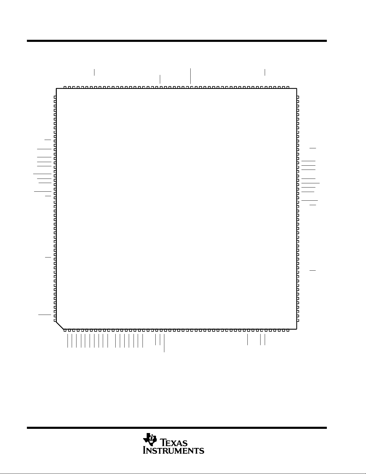
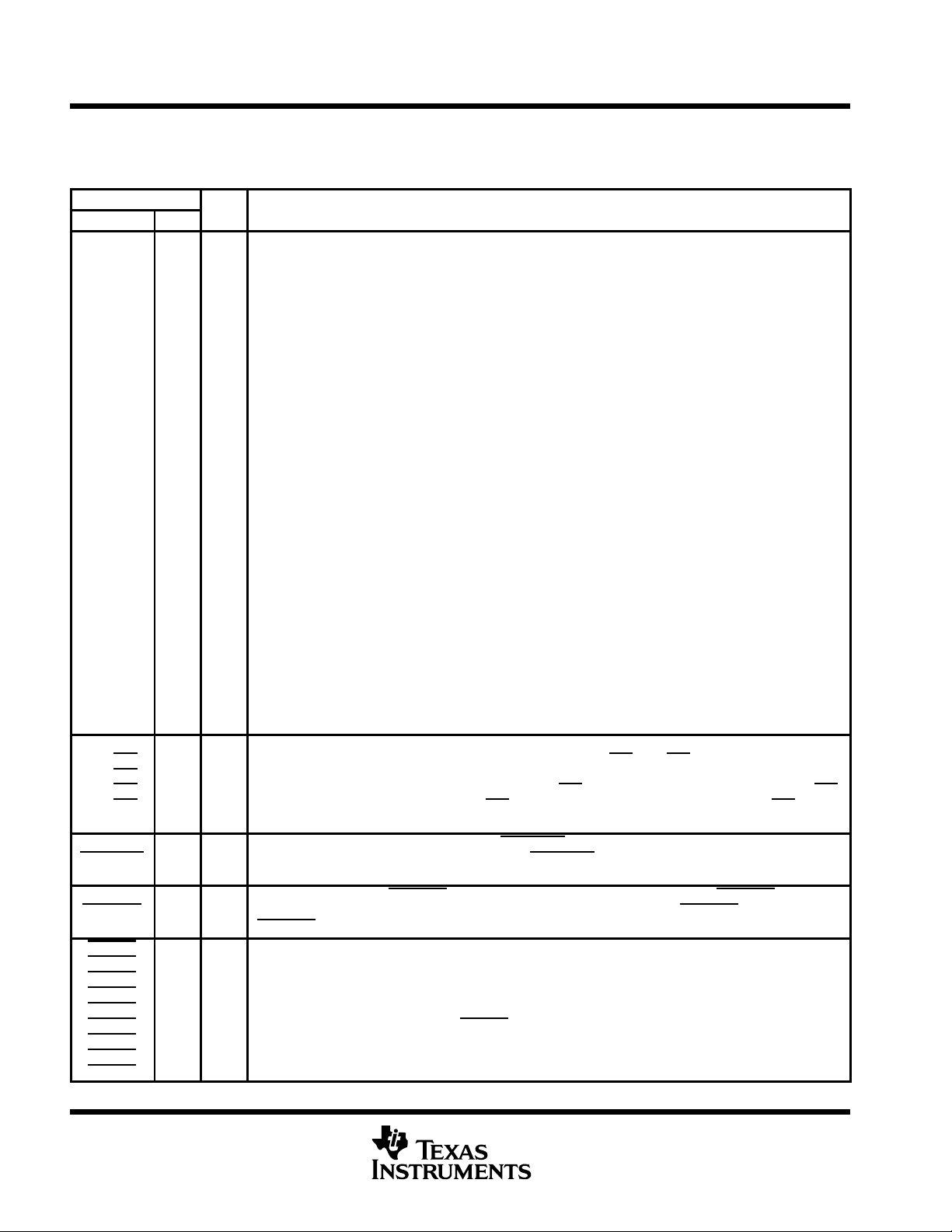
PDV LOW-PROFILE QUAD FLAT PACKAGE
TOP VIEW
V
CC
GND
S_AD11
GND
S_AD12
S_AD13
V
CC
S_AD14
S_AD15
GND
S_C/BE1
S_PAR
S_SERR
V
CC
S_PERR
S_LOCK
S_STOP
GND
S_DEVSEL
S_TRDY
S_IRDY
V
CC
S_FRAME
S_C/BE2
GND
S_AD16
S_AD17
V
CC
S_AD18
S_AD19
GND
S_AD20
S_AD21
V
CC
S_AD22
S_AD23
GND
S_C/BE3
S_AD24
V
CC
S_AD25
S_AD26
GND
S_AD27
S_AD28
V
CC
S_AD29
S_AD30
GND
S_AD31
S_REQ0
V
CC
CONFIG66
MSK_IN
HSENUM
126
125
127
CCP
P_V
124
GND
123
P_AD1
P_AD0
122
121
CC
V
120
P_AD2
P_AD3
118
119
GND
117
P_AD4
P_AD5
116
115
CC
V
114
P_AD6
P_AD7
112
113
CCP
GND
148
S_AD7
S_AD6
146
147
V
145
CC
S_AD4
S_AD5
144
143
CC
V
S_M66ENA
S_AD10
S_AD9
S_C/BE0
154
153
152
151
S_AD8
150
149
MS0
155
214365871091211141316151817201922212423262528273029323134333635383740394241444346454847504952
157
158
159
160
161
162
163
164
165
166
167
168
169
170
171
172
173
174
175
176
177
178
179
180
181
182
183
184
185
186
187
188
189
190
191
192
193
194
195
196
197
198
199
200
201
202
203
204
205
206
207
208
GND
156
GND
142
S_AD2
S_AD3
140
141
CC
V
139
S_AD0
S_AD1
138
137
GND
136
S_V
135
TMS
TCK
TRST
132
134
133
PCI2050A
CC
V
131
TDO
130
TDI
129
HSLED
128
GND
P_C/BE0
111
110
CC
V
P_AD8
108
109
P_AD9
MS1
107
51 106
CC
V
105
104
103
102
101
100
99
98
97
96
95
94
93
92
91
90
89
88
87
86
85
84
83
82
81
80
79
78
77
76
75
74
73
72
71
70
69
68
67
66
65
64
63
62
61
60
59
58
57
56
55
54
53
GND
V
CC
P_M66ENA
P_AD10
GND
P_AD11
P_AD12
V
CC
P_AD13
P_AD14
GND
P_AD15
P_C/BE1
V
CC
P_PAR
P_SERR
P_PERR
P_LOCK
GND
P_STOP
P_DEVSEL
P_TRDY
P_IRDY
V
CC
P_FRAME
P_C/BE2
GND
P_AD16
P_AD17
V
CC
P_AD18
P_AD19
GND
P_AD20
P_AD21
V
CC
P_AD22
P_AD23
GND
P_IDSEL
P_C/BE3
P_AD24
V
CC
P_AD25
P_AD26
GND
P_AD27
P_AD28
V
CC
P_AD29
GND
V
CC
CC
V
S_REQ2
S_REQ3
S_REQ4
S_REQ6
S_REQ5
S_REQ1
2
S_GNT0
S_REQ7
S_REQ8
GND
S_GNT1
S_GNT2
S_GNT3
S_GNT4
POST OFFICE BOX 655303 • DALLAS, TEXAS 75265
S_GNT5
S_GNT6
S_GNT7
GND
S_CLK
S_GNT8
V
GPIO2
S_RST
S_CFN
GP103/HSSWITCH
CC
GPIO0
GPIO1
S_CLKOUT0
GND
S_CLKOUT1
S_CLKOUT2
S_CLKOUT3
CC
V
S_CLKOUT4
GND
S_CLKOUT6
S_CLKOUT5
S_CLKOUT7
CC
V
S_CLKOUT8
S_CLKOUT9
P_RST
BPCCE
P_CLK
P_GNT
P_REQ
GND
P_AD31
CC
V
P_AD30
GND
primary PCI system terminals
I/O
DESCRIPTION
I/O
DESCRIPTION
TERMINAL
NAME NO.
P_CLK 45 I
P_RST
43 I
Primary PCI bus clock. P_CLK provides timing for all transactions on the primary PCI bus. All primary PCI signals
are sampled at rising edge of P_CLK.
PCI reset. When the primary PCI bus reset is asserted, P_RST causes the bridge to put all output buffers in a
high-impedance state and reset all internal registers. When asserted, the device is completely nonfunctional.
During P_RST
, the secondary interface is driven low. After P_RST is deasserted, the bridge is in its default state.
primary PCI address and data terminals
TERMINAL
NAME NO.
P_AD31
P_AD30
P_AD29
P_AD28
P_AD27
P_AD26
P_AD25
P_AD24
P_AD23
P_AD22
P_AD21
P_AD20
P_AD19
P_AD18
P_AD17
P_AD16
P_AD15
P_AD14
P_AD13
P_AD12
P_AD11
P_AD10
P_AD9
P_AD8
P_AD7
P_AD6
P_AD5
P_AD4
P_AD3
P_AD2
P_AD1
P_AD0
P_C/BE3
P_C/BE2
P_C/BE1
P_C/BE0
49
50
55
57
58
60
61
63
67
68
70
71
73
74
76
77
93
95
96
98
99
101
107
109
112
113
115
116
118
119
121
122
64
79
92
110
Primary address/data bus. These signals make up the multiplexed PCI address and data bus on the primary
interface. During the address phase of a primary bus PCI cycle, P_AD31–P_AD0 contain a 32-bit address
I/O
or other destination information. During the data phase, P_AD31–P_AD0 contain data.
Primary bus commands and byte enables. These signals are multiplexed on the same PCI terminals. During
the address phase of a primary bus PCI cycle, P_C/BE3
phase, this 4-bit bus is used as byte enables. The byte enables determine which byte paths of the full 32-bit
I/O
data bus carry meaningful data. P_C/BE0 applies to byte 0 (P_AD7–P_AD0), P_C/BE1 applies to byte 1
(P_AD15–P_AD8), P_C/BE2
(P_AD31–P_AD24).
PCI2050A
PCI-to-PCI BRIDGE
SCPS067 – MAY 2001
Terminal Functions
–P_C/BE0 define the bus command. During the data
applies to byte 2 (P_AD23–P_AD16), and P_C/BE3 applies to byte 3
POST OFFICE BOX 655303 • DALLAS, TEXAS 75265
3
PCI2050A
I/O
DESCRIPTION
PCI-to-PCI BRIDGE
SCPS067 – MAY 2001
Terminal Functions (Continued)
primary PCI interface control terminals
TERMINAL
NAME NO.
Primary device select. The bridge asserts P_DEVSEL to claim a PCI cycle as the target device. As a PCI
P_DEVSEL 84 I/O
P_FRAME
P_GNT
P_IDSEL 65 I
P_IRDY 82 I/O
P_LOCK 87 I/O Primary PCI bus lock. P_LOCK is used to lock the primary bus and gain exclusive access as a bus master .
P_PAR 90 I/O
P_PERR
P_REQ 47 O Primary PCI bus request. Asserted by the bridge to request access to the primary PCI bus as a master.
P_SERR 89 O
P_STOP 85 I/O
P_TRDY 83 I/O
80 I/O
46 I
88 I/O
master on the primary bus, the bridge monitors P_DEVSEL
before time-out occurs, then the bridge terminates the cycle with a master abort.
Primary cycle frame. P_FRAME is driven by the master of a primary bus cycle. P_FRAME is asserted to
indicate that a bus transaction is beginning, and data transfers continue while this signal is asserted. When
P_FRAME is deasserted, the primary bus transaction is in the final data phase.
Primary bus grant to bridge. P_GNT is driven by the primary PCI bus arbiter to grant the bridge access to the
primary PCI bus after the current data transaction has completed. P_GNT
bus request, depending on the primary bus arbitration algorithm.
Primary initialization device select. P_IDSEL selects the bridge during configuration space accesses.
P_IDSEL can be connected to one of the upper 24 PCI address lines on the primary PCI bus.
Note: There is no IDSEL signal interfacing the secondary PCI bus; thus, the entire configuration space of the
bridge can only be accessed from the primary bus.
Primary initiator ready. P_IRDY indicates ability of the primary bus master to complete the current data phase
of the transaction. A data phase is completed on a rising edge of P_CLK where both P_IRDY
are asserted. Until P_IRDY and P_TRDY are both sampled asserted, wait states are inserted.
Primary parity. In all primary bus read and write cycles, the bridge calculates even parity across the P_AD
and P_C/BE
one-P_CLK delay . As a target during PCI read cycles, the calculated parity is compared to the parity indicator
of the master; a miscompare can result in a parity error assertion (P_PERR).
Primary parity error indicator. P_PERR is driven by a primary bus PCI device to indicate that calculated parity
does not match P_PAR when P_PERR
Primary system error. Output pulsed from the bridge when enabled through the command register (PCI offset
04h). indicating a system error has occurred. The bridge needs not be the target of the primary PCI cycle to
assert this signal. When bit 6 is enabled in the bridge control register (PCI offset 3Eh), this signal also pulses,
indicating that a system error has occurred on one of the subordinate buses downstream from the bridge.
Primary cycle stop signal. This signal is driven by a PCI target to request that the master stop the current
primary bus transaction. This signal is used for target disconnects and is commonly asserted by target devices
which do not support burst data transfers.
Primary target ready. P_TRDY indicates the ability of the primary bus target to complete the current data
phase of the transaction. A data phase is completed upon a rising edge of P_CLK where both P_IRDY
P_TRDY
buses. As a bus master during PCI write cycles, the bridge outputs this parity indicator with a
is enabled through bit 6 of the command register (PCI offset 04h).
are asserted. Until both P_IRDY and P_TRDY are asserted, wait states are inserted.
until a target responds. If no target responds
may or may not follow a primary
and P_TRDY
and
4
POST OFFICE BOX 655303 • DALLAS, TEXAS 75265
secondary PCI system terminals
I/O
DESCRIPTION
TERMINAL
NAME NO.
S_CLKOUT9
S_CLKOUT8
S_CLKOUT7
S_CLKOUT6
S_CLKOUT5
S_CLKOUT4
S_CLKOUT3
S_CLKOUT2
S_CLKOUT1
S_CLKOUT0
S_CLK
S_CFN 23 I
S_RST 22 O
42
41
39
38
36
35
33
32
30
29
21 I Secondary PCI bus clock input. This input synchronizes the PCI2050 to the secondary bus clocks.
Secondary PCI bus clocks. Provide timing for all transactions on the secondary PCI bus. Each secondary
O
bus device samples all secondary PCI signals at the rising edge of its corresponding S_CLKOUT input.
Secondary external arbiter enable. When this signal is high, the secondary external arbiter is enabled. When
the external arbiter is enabled, the PCI2050 S_REQ0
to the bridge and S_GNT0
secondary bus.
Secondary PCI reset. S_RST is a logical OR of P_RST and the state of the secondary bus reset bit (bit 6)
of the bridge control register (PCI offset 3Eh). S_RST
secondary interface CLK signal.
PCI2050A
PCI-to-PCI BRIDGE
SCPS067 – MAY 2001
Terminal Functions (Continued)
terminal is reconfigured as a secondary bus grant input
is reconfigured as a secondary bus master request to the external arbiter on the
is asynchronous with respect to the state of the
POST OFFICE BOX 655303 • DALLAS, TEXAS 75265
5
PCI2050A
I/O
DESCRIPTION
PCI-to-PCI BRIDGE
SCPS067 – MAY 2001
Terminal Functions (Continued)
secondary PCI address and data terminals
TERMINAL
NAME NO.
S_AD31
S_AD30
S_AD29
S_AD28
S_AD27
S_AD26
S_AD25
S_AD24
S_AD23
S_AD22
S_AD21
S_AD20
S_AD19
S_AD18
S_AD17
S_AD16
S_AD15
S_AD14
S_AD13
S_AD12
S_AD11
S_AD10
S_AD9
S_AD8
S_AD7
S_AD6
S_AD5
S_AD4
S_AD3
S_AD2
S_AD1
S_AD0
S_C/BE3
S_C/BE2
S_C/BE1
S_C/BE0
S_DEVSEL 175 I/O
S_FRAME 179 I/O
S_GNT8
S_GNT7
S_GNT6
S_GNT5
S_GNT4
S_GNT3
S_GNT2
S_GNT1
S_GNT0
206
204
203
201
200
198
197
195
192
191
189
188
186
185
183
182
165
164
162
161
159
154
152
150
147
146
144
143
141
140
138
137
194
180
167
149
19
18
17
16
15
14
13
11
10
Secondary address/data bus. These signals make up the multiplexed PCI address and data bus on the
secondary interface. During the address phase of a secondary bus PCI cycle, S_AD31–S_AD0 contain a
I/O
32-bit address or other destination information. During the data phase, S_AD31–S_AD0 contain data.
Secondary bus commands and byte enables. These signals are multiplexed on the same PCI terminals.
During the address phase of a secondary bus PCI cycle, S_C/BE3
During the data phase, this 4-bit bus is used as byte enables. The byte enables determine which byte paths
I/O
of the full 32-bit data bus carry meaningful data. S_C/BE0 applies to byte 0 (S_AD7–S_AD0), S_C/BE1
applies to byte 1 (S_AD15–S_AD8), S_C/BE2 applies to byte 2 (S_AD23–S_AD16), and S_C/BE3 applies
to byte 3 (S_AD31–S_AD24).
Secondary device select. The bridge asserts S_DEVSEL to claim a PCI cycle as the target device. As a PCI
master on the secondary bus, the bridge monitors S_DEVSEL
before time-out occurs, then the bridge terminates the cycle with a master abort.
Secondary cycle frame. S_FRAME is driven by the master of a secondary bus cycle. S_FRAME is asserted
to indicate that a bus transaction is beginning and data transfers continue while S_FRAME
S_FRAME
Secondary bus grant to the bridge. The bridge provides internal arbitration and these signals are used to grant
potential secondary PCI bus masters access to the bus. Ten potential masters (including the bridge) can be
located on the secondary PCI bus.
O
When the internal arbiter is disabled, S_GNT0
for the bridge.
is deasserted, the secondary bus transaction is in the final data phase.
–S_C/BE0 define the bus command.
until a target responds. If no target responds
is asserted. When
is reconfigured as an external secondary bus request signal
6
POST OFFICE BOX 655303 • DALLAS, TEXAS 75265

PCI2050A
I/O
DESCRIPTION
PCI-to-PCI BRIDGE
SCPS067 – MAY 2001
Terminal Functions (Continued)
secondary PCI interface control terminals
TERMINAL
NAME NO.
Secondary initiator ready. S_IRDY indicates the ability of the secondary bus master to complete the current
S_IRDY 177 I/O
S_LOCK 172 I/O Secondary PCI bus lock. S_LOCK is used to lock the secondary bus and gain exclusive access as a master .
S_PAR 168 I/O
S_PERR
S_REQ8
S_REQ7
S_REQ6
S_REQ5
S_REQ4
S_REQ3
S_REQ2
S_REQ1
S_REQ0
S_SERR
S_STOP 173 I/O
S_TRDY 176 I/O
171 I/O
9
8
7
6
5
4
3
2
207
169 I
data phase of the transaction. A data phase is completed on a rising edge of S_CLK where both S_IRDY
S_TRDY
Secondary parity. In all secondary bus read and write cycles, the bridge calculates even parity across the S_AD
and S_C/BE
one-S_CLK delay. As a target during PCI read cycles, the calculated parity is compared to the master parity
indicator. A miscompare can result in a parity error assertion (S_PERR).
Secondary parity error indicator. S_PERR is driven by a secondary bus PCI device to indicate that calculated
parity does not match S_PAR when enabled through the command register (PCI offset 04h).
Secondary PCI bus request signals. The bridge provides internal arbitration, and these signals are used as
inputs from secondary PCI bus masters requesting the bus. Ten potential masters (including the bridge) can
be located on the secondary PCI bus.
I
When the internal arbiter is disabled, the S_REQ0
for the bridge.
Secondary system error. S_SERR is passed through the primary interface by the bridge if enabled through the
bridge control register (PCI offset 3Eh). S_SERR
Secondary cycle stop signal. S_STOP is driven by a PCI target to request that the master stop the current
secondary bus transaction. S_STOP
that do not support burst data transfers.
Secondary target ready. S_TRDY indicates the ability of the secondary bus target to complete the current data
phase of the transaction. A data phase is completed on a rising edge of S_CLK where both S_IRDY
S_TRDY
are asserted; until S_IRDY and S_TRDY are asserted, wait states are inserted.
buses. As a master during PCI write cycles, the bridge outputs this parity indicator with a
signal is reconfigured as an external secondary bus grant
is never asserted by the bridge.
is used for target disconnects and is commonly asserted by target devices
are asserted; until S_IRDY and S_TRDY are asserted, wait states are inserted.
and
and
POST OFFICE BOX 655303 • DALLAS, TEXAS 75265
7

PCI2050A
I/O
DESCRIPTION
I/O
DESCRIPTION
PCI-to-PCI BRIDGE
SCPS067 – MAY 2001
miscellaneous terminals
TERMINAL
NAME NO.
Bus/power clock control management terminal. When signal BPCCE is tied high, and when the
BPCCE 44 I
GPIO3/HSSWITCH
GPIO2
GPIO1
GPIO0
HSENUM 127 O Hot–swap ENUM
HSLED 128 O Hot-swap LED output
MS0
MS1
P_M66ENA 102 I
CONFIG66 125 I
S_M66ENA 153 I/O
24
25
27
28
155 I Mode select 0
106 I Mode select 1
PCI2050 is placed in the D3 power state, it enables the PCI2050 to place the secondary bus in the
B2 power state. The PCI2050 disables the secondary clocks and drives them to 0. When tied low,
placing the PCI2050 in the D3 power state has no effect on the secondary bus clocks.
General-purpose I/O terminals
GPIO3 is HSSWITCH
I
HSSWITCH
Primary interface 66 MHz enable. This input-only signal pin is used to designate the primary interface
bus speed. This signal should be pulled low for 33 MHz operation on the primary bus. In this case
S_M66ENA signal will be driven low by the PCI2050A, forcing the secondary bus to run at 33 MHz.
For 66-MHz operation, this signal should be pulled high.
Configure 66 MHz operation. This input-only pin is used to specify if PCI2050A is capable of running
at 66 MHz. If this terminal is tied high, then device can be run at 66 MHz. If this pin is tied low, then
PCI2050A can only function under the 33 MHz PCI specification.
Secondary 66-MHz enable terminal. This signal is used to designate the secondary bus speed. If the
P_M66ENA is driven low, then this signal is driven low by the PCI2050A forcing secondary bus to run
at 33 MHz. If the primary bus is running at 66 MHz (P_M66ENA is high), then S_M66ENA is an input
and should be externally pulled high for the secondary bus to operate at 66 MHz or pulled low for
secondary bus to operate at 33 MHz. Note that S_M66ENA is an open drained output.
Terminal Functions (Continued)
in cPCI mode.
provides the status of the ejector handle switch to the cPCI logic.
JTAG interface terminals
TERMINAL
NAME NO.
TCK 133 I JTAG boundary-scan clock. TCK is the clock controlling the JTAG logic.
TDI 129 I
TDO 130 O
TMS 132 I JTAG test mode select. TMS causes state transitions in the test access port controller.
TRST 134 I
JTAG serial data in. TDI is the serial input through which JTAG instructions and test data enter the JTAG
interface. The new data on TDI is sampled on the rising edge of TCK.
JTAG serial data out. TDO is the serial output through which test instructions and data from the test logic
leave the PCI2050.
JTAG T AP reset. When TRST is asserted low, the T AP controller is asynchronously forced to enter a reset
state and initialize the test logic.
8
POST OFFICE BOX 655303 • DALLAS, TEXAS 75265

power supply terminals
DESCRIPTION
TERMINAL
NAME NO.
12, 20, 31, 37, 48, 52, 54,
59, 66, 72, 78, 86, 94, 100,
104, 111, 117, 123, 136,
142, 148, 156, 158, 160,
166, 174, 181, 187, 193,
199, 205
1, 26, 34, 40, 51, 53, 56, 62,
69, 75, 81, 91, 97, 103, 105,
108, 114, 120, 131, 139,
145, 151, 157, 163, 170,
178, 184, 190, 196, 202,
208
124
135
P_V
S_V
GND
V
CC
CCP
CCP
Terminal Functions (Continued)
Device ground terminals
Power-supply terminal for core logic (3.3 V)
Primary bus-signaling environment supply. P_V
I/O signals.
Secondary bus-signaling environment supply. S_V
bus I/O signals.
CCP
PCI2050A
PCI-to-PCI BRIDGE
SCPS067 – MAY 2001
is used in protection circuitry on primary bus
is used in protection circuitry on secondary
CCP
detailed description
The PCI2050 is a bridge between two PCI buses and is compliant with both the PCI local bus specification and
the PCI-to-PCI bridge specification. The bridge supports two 32-bit PCI buses operating at a maximum of 66
MHz. The primary and secondary buses operate independently in either 3.3-V or 5-V signaling environment.
The core logic of the bridge, however, is powered at 3.3 V to reduce power consumption.
Host software interacts with the bridge through internal registers. These registers provide the standard PCI
status and control for both the primary and secondary buses. Many vendor-specific features that exist in the
TI extension register set are included in the bridge. The PCI configuration header of the bridge is only accessible
from the primary PCI interface.
The bridge provides internal arbitration for the nine possible bus masters, and provides each with a dedicated
active low request/grant pair (REQ
bridge defaulting to the highest priority tier. The PCI2050A also supports external arbitration.
Upon system power up, power-on self test (POST) software configures the bridge according to the devices that
exist on subordinate buses, and enables performance-enhancing features of the PCI2050. In a typical system,
this is the only communication with the bridge internal register set.
write combining
PCI2050A supports write combining for upstream and downstream transactions. This feature is used to
combine separate sequential memory write transactions into a single burst transactions. This feature can only
be used if the address of the next memory write transaction is the next sequential address after the address
of the last double word of the previous memory transaction. For example if the current memory transaction ends
at address X and next memory transaction starts at address X+1, then PCI2050A combines both transactions
into a single transaction.
/GNT). The arbiter features a two-tier rotational scheme with the PCI2050A
The write combining feature of PCI2050A is enabled by default on power on reset. It can also be disabled by
setting bit 0 of the TI diagnostics register at offset F0h to 1.
POST OFFICE BOX 655303 • DALLAS, TEXAS 75265
9

PCI2050A
PCI-to-PCI BRIDGE
SCPS067 – MAY 2001
detailed description (continued)
66-MHz operation
PCI2050A supports two 32-bit PCI buses operating at a maximum frequency of 66-MHz. The 66-MHz clocking
requires three terminals P_M66ENA, S_M66ENA and CONFIG66. To enable 66 MHz operation, the signal
CONFIG66 must be tied high on the board. This sets the 66 MHz capable bit in the primary and secondary status
register. The P_M66ENA and S_M66ENA must not be pulled high unless CONFIG66 is also high.
The signals P_ M66ENA and S_ M66ENA indicate whether the primary or secondary interfaces are working
at 66 MHz. This information is needed to control the frequency of the secondary bus. Note that PCI local bus
specification 2.2 restricts clock frequency changes above 33 MHz to during reset only.
The following frequency combinations are supported on the primary and secondary buses in PCI2050A:
D
66 MHz primary bus, 66 MHz secondary bus
D
66 MHz primary bus, 33 MHz secondary bus
D
33 MHz primary bus, 33 MHz secondary bus
The PCI2050A does not support 33-MHz primary/66-MHz secondary bus operation. If CONFIG66 is high and
P_M66ENA is low , the PCI2050A pulls down S_M66ENA to indicate that secondary bus is running at 33 MHz.
The 2050A generates the clock signals S_CLKOUT[9:0] for the secondary bus devices and its own interface.
It divides the P_CLK by two to generate the secondary clock outputs whenever the primary bus is running at
66 MHz and secondary bus is running at 33 MHz. The bridge detects this condition by polling P_M66ENA and
S_M66ENA.
10
POST OFFICE BOX 655303 • DALLAS, TEXAS 75265

PCI2050A
PCI-to-PCI BRIDGE
SCPS067 – MAY 2001
bridge configuration header
The bridge configuration header for PCI2050A is exactly the same as the bridge configuration header for PCI2050
except for the following registers.
The PCI2050A bridge is a single-function PCI device. The configuration header is in compliance with the PCI-to-PCI
Bridge Specification 1.1. Table 1 shows the PCI configuration header, which includes the predefined portion of the
bridge configuration space. The PCI configuration offset is shown in the right column under the OFFSET heading.
Table 1. Bridge Configuration Header
REGISTER NAME OFFSET
Device ID Vendor ID 00h
Status Command 04h
Class code Revision ID 08h
BIST Header type Primary latency timer Cache line size 0Ch
Base address 0 10h
Base address 1 14h
Secondary bus latency timer Subordinate bus number Secondary bus number Primary bus number 18h
Secondary status I/O limit I/O base 1Ch
Memory limit Memory base 20h
Prefetchable memory limit Prefetchable memory base 24h
Prefetchable base upper 32 bits 28h
Prefetchable limit upper 32 bits 2Ch
I/O limit upper 16 bits I/O base upper 16 bits 30h
Reserved Capability pointer 34h
Expansion ROM base address 38h
Bridge control Interrupt pin Interrupt line 3Ch
Arbiter control Extended diagnostic Chip control 40h
Reserved 44h–60h
GPIO input data GPIO output enable GPIO output data P_SERR event disable 64h
Reserved P_SERR status Secondary clock control 68h
Reserved 6Ch–D8h
Power management capabilities PM next item pointer PM capability ID DCh
Data PMCSR bridge support Power management control/status E0h
Reserved Hot swap control status HS next item pointer HS capability ID E4h
Reserved E8h–EFh
Reserved Diagnostics F0
Reserved F4–FF
POST OFFICE BOX 655303 • DALLAS, TEXAS 75265
11

PCI2050A
PCI-to-PCI BRIDGE
SCPS067 – MAY 2001
bridge configuration header (continued)
status register
The bit 5 in status register is hardwired to 0 in PCI2050. However, in PCI2050A it indicates whether the primary
PCI interface is 66-MHz capable or not.
Bit 15 14 13 12 11 10 9 8 7 6 5 4 3 2 1 0
Name Status
Type R/W R/W R/W R/W R/W R R R/W R R R R R R R R
Default 0 0 0 0 0 0 1 0 1 0 0 1 0 0 0 0
Register: Status
Type: Read-only, read/write (see individual bit descriptions)
Offset: 06h
Default: 0290h
Table 2. Status Register
BIT TYPE FUNCTION
15-6
4-0
Same as
PCI2050
5 R
Same as
PCI2050
Same as PCI2050.
66-MHz capable. Bit 5 indicates whether the primary interface is 66 MHz capable. It reads as 0 when CONFIG66 is tied
low to indicate that PCI2050A is not 66-MHz capable and reads as 1 when CONFIG66 is tied high to indicate that the
primary bus is 66-MHz capable.
Same as PCI2050.
revision ID register
The revision ID register indicates the silicon version of PCI2050A.
Bit 7 6 5 4 3 2 1 0
Name Revision ID
Type R R R R R R R R
Default 0 0 0 0 0 0 0 1
Register: Revision ID
Type: Read-only
Offset: 08h
Default: 01h
12
POST OFFICE BOX 655303 • DALLAS, TEXAS 75265

PCI-to-PCI BRIDGE
SCPS067 – MAY 2001
bridge configuration header (continued)
secondary status register
The bit 5 in the status register is hardwired to 0 in PCI2050. However, in PCI2050A it indicates whether the
primary PCI interface is 66-MHz capable.
Bit 15 14 13 12 11 10 9 8 7 6 5 4 3 2 1 0
Name Secondary Status
Type R/W R/W R/W R/W R/W R R R/W R R R R R R R R
Default 0 0 0 0 0 0 1 0 0 0 0 0 0 0 0 0
Register: Secondary Status
Type: Read-only, read/write (see individual bit descriptions)
Offset: IEh
Default: 0200
Table 3. Status Register
BIT TYPE FUNCTION
15-6
5 R
4-0
Same as
PCI2050
Same as
PCI2050
Same as PCI2050.
66-MHz capable. Bit 5 indicates whether the primary interface is 66-MHz capable. It reads as 0 when CONFIG66 is tied
low to indicate that PCI2050A is not 66 MHz capable and reads as 1 when CONFIG66 is tied high to indicate that the
primary bus is 66-MHz capable.
Same as PCI2050.
PCI2050A
extension registers
The extension registers for PCI2050A are exactly the same as the extension registers for PCI2050 except for
the following registers.
diagnostics register
The register is used to enable or disable posted write combing of PCI2050A.
Bit 15 14 13 12 11 10 9 8 7 6 5 4 3 2 1 0
Name TI Diagnostics
Type R R R R R R R R R R R R R R R R/W
Default 0 0 0 0 0 0 1 0 0 0 0 0 0 0 0 0
Register: TI Diagnostics
Type: Read-only, read/write (see individual bit descriptions)
Offset: F0h
Default: 0000h
Table 4. TI Diagnostics Register
BIT TYPE FUNCTION
15-6 R Reserved. Bit 15–1 return 0s when read.
Disable posted write combining.
0 R/W
0: Enable posted write combining (Default)
1: Disable posted write combining
POST OFFICE BOX 655303 • DALLAS, TEXAS 75265
13
PCI2050A
(3)
PCI-to-PCI BRIDGE
SCPS067 – MAY 2001
electrical data
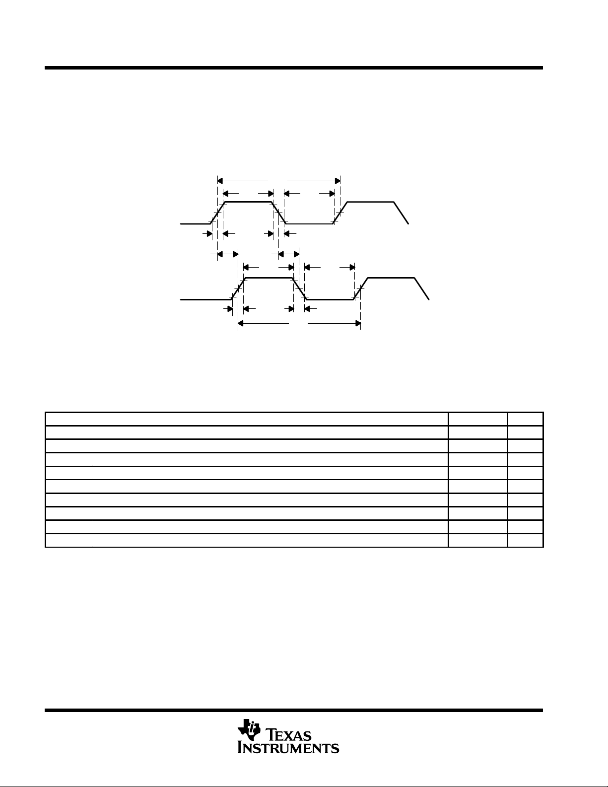
66-MHz PCI clock signal ac parameters
The ac specification consists of input requirements and output responses. The input requirements consists of
setup and hold times, pulse widths, and high and low times. Output responses are delays from clock to signal.
The ac specifications are defined are separately for each clock domain within the PCI2050A.
Figure 1 shows the ac parameters measurements for P_CLK and S_CLK signals.
t
c
P_CLK
S_CLK
t
t(1)
h
t
r
t
s
t
h
t
r
V
t(1)
V
t(2)
V
t(3)
t
r
t
s
V
V
t(2)
V
t(3)
t
r
t
l
t
l
t
c
NOTE: V
– 2.0 V for 5-V clocks; 0.5 VCC for 3.3-V clocks
t(1)
V
– 1.5 V for 5-V clocks; 0.4 VCC for 3.3-V clocks
t(2)
V
– 0.8 V for 5-V clocks; 0.3 VCC for 3.3-V clocks
t
Figure 1. PCI Clock Signal AC Parameter Measurements
66 MHz PCI clock signal ac parameters
t
c
t
(h)
t
(l)
t
(PSS)
t
d(SCLK)
t
r(SCLK)
t
f(SCLK)
t
d(skew)
t
sk
P_CLK, S_CLK cycle time 15 30 ns
P_CLK, S_CLK high time 6 ns
P_CLK, S_CLK low time 6 ns
P_CLK, S_CLK slew rate (0.2 Vcc to 0.6 Vcc) 1.5 4 V/ns
Delay from P_CLK to S_CLK 0 7 ns
P_CLK rising to S_CLK rising 0 7 ns
P_CLK falling to S_CLK falling 0 7 ns
S_CLK0 duty cycle skew from P_CLK duty cycle 0.750 ns
S_CLKx to SCLKy 0.500 ns
PARAMETER MIN MAX UNIT
14
POST OFFICE BOX 655303 • DALLAS, TEXAS 75265

electrical data (continued)
66-MHz PCI signal timing specifications
Figure 2 illustrates the PCI signal timing specification.
PCI2050A
PCI-to-PCI BRIDGE
SCPS067 – MAY 2001
CLK
Output
Input
NOTE: V
– 1.5 V for 5-V signals; 0.4 VCC for 3.3-V signals
test
66-MHz PCI signal timing
t
v(bus)
t
v(ptp)
t
on
t
off
t
su(bus)
t
su(ptp)
t
h
NOTES: 1. See Figure 2
CLK to signal valid delay - bused signals (see Notes 1, 2, and 3) 2 6 ns
CLK to signal valid delay – point to point (see Notes 1, 2, and 3) 2 6 ns
Float to active delay (see Notes 1, 2, and 3) 2 ns
Active to float delay (see Notes 1, 2, and 3) 14 ns
Input setup time to CLK– bused signal (see Notes 1, 2, and 3) 3 ns
Input setup time to CLK – point-to-point (see Notes 1, 2, and 3) 5 ns
Input signal hold time from CLK (see Notes 1 and 2) 0 ns
2. All primary interface signals are synchronized to P_CLK and all secondary interface signals are synchronized to S_CLK.
3. Bused signals are as follows:
P_AD, P_C/BE
S_C/BE
, P_PAR, P_PERR, P_SERR, P_FRAME, P_IRDY, P_TRDY, P_LOCK, P_DEVSEL, P_STOP, P_IDSEL, S_AD,
, S_PAR, S_PERR, S_SERR, S_FRAME, S_IRDY, S_TRDY, S_LOCK, S_DEVSEL, S_STOP
V
test
t
v
Valid
t
on
t
su
Valid
t
(inval)
t
off
t
h
Figure 2. PCI Signal Timing Measurement Conditions
PARAMETER MIN MAX UNIT
Point-to-point signals are as follows:
P_REQ
, S_REQx, P_GNT, S_GNTx
POST OFFICE BOX 655303 • DALLAS, TEXAS 75265
15

PCI2050A
PCI-to-PCI BRIDGE
SCPS067 – MAY 2001
MECHANICAL DATA
PDV (S-PQFP-G208) PLASTIC QUAD FLATPACK
157
208
156
1
105
52
104
53
0,27
0,17
0,50
0,08
M
0,13 NOM
Gage Plane
25,50 TYP
28,05
SQ
27,95
30,20
SQ
29,80
1,45
1,35
1,60 MAX
NOTES: A. All linear dimensions are in millimeters.
B. This drawing is subject to change without notice.
C. Falls within JEDEC MS-026
0,05 MIN
0,25
0°-7°
0,75
0,45
Seating Plane
0,08
4087729/D 11/98
16
POST OFFICE BOX 655303 • DALLAS, TEXAS 75265

IMPORTANT NOTICE
T exas Instruments and its subsidiaries (TI) reserve the right to make changes to their products or to discontinue
any product or service without notice, and advise customers to obtain the latest version of relevant information
to verify, before placing orders, that information being relied on is current and complete. All products are sold
subject to the terms and conditions of sale supplied at the time of order acknowledgment, including those
pertaining to warranty, patent infringement, and limitation of liability.
TI warrants performance of its products to the specifications applicable at the time of sale in accordance with
TI’s standard warranty . T esting and other quality control techniques are utilized to the extent TI deems necessary
to support this warranty . Specific testing of all parameters of each device is not necessarily performed, except
those mandated by government requirements.
Customers are responsible for their applications using TI components.
In order to minimize risks associated with the customer’s applications, adequate design and operating
safeguards must be provided by the customer to minimize inherent or procedural hazards.
TI assumes no liability for applications assistance or customer product design. TI does not warrant or represent
that any license, either express or implied, is granted under any patent right, copyright, mask work right, or other
intellectual property right of TI covering or relating to any combination, machine, or process in which such
products or services might be or are used. TI’s publication of information regarding any third party’s products
or services does not constitute TI’s approval, license, warranty or endorsement thereof.
Reproduction of information in TI data books or data sheets is permissible only if reproduction is without
alteration and is accompanied by all associated warranties, conditions, limitations and notices. Representation
or reproduction of this information with alteration voids all warranties provided for an associated TI product or
service, is an unfair and deceptive business practice, and TI is not responsible nor liable for any such use.
Resale of TI’s products or services with
that product or service voids all express and any implied warranties for the associated TI product or service,
is an unfair and deceptive business practice, and TI is not responsible nor liable for any such use.
Also see: Standard T erms and Conditions of Sale for Semiconductor Products.
Copyright 2001, Texas Instruments Incorporated
statements different from or beyond the parameters
www.ti.com/sc/docs/stdterms.htm
Mailing Address:
Texas Instruments
Post Office Box 655303
Dallas, Texas 75265
stated by TI for
 Loading...