

Page 1

User's Guide
SLLU256–October 2016
ONET1131EC Evaluation Module
This document describes the main features and functionality of the evaluation module (EVM) board for the
devices.
The ONET1131EC is a 11.7-Gbps transceiver with an integrated limiting amplifier and a modulator driver.
The EVM can be used to evaluate the performance of the parts in conjunction with an electroabsorptive
modulated laser (EML) transmit optical subassembly (TOSA) and a receive optical subassembly (ROSA)
in standard XMD-compliant packages.
The EVM is controlled with a graphical user interface (GUI).
Throughout this document, the images shown may represent the ONET1130Ex. Those images are
representative of the boards and parts on the ONET1131EC.
spacer
Contents
1 Hardware and Equipment................................................................................................... 2
2 EVM Block Diagram ......................................................................................................... 2
3 EVM Connections............................................................................................................ 3
4 Measurement Setup......................................................................................................... 6
4.1 Open Loop Operation Without Fault Detection or Digital Monitoring ........................................ 8
4.2 Closed Loop Operation with Fault Detection and Digital Monitoring ....................................... 10
5 LED Indicators .............................................................................................................. 13
6 Typical Performance Results ............................................................................................. 13
7 Schematics and Bill of Materials ......................................................................................... 15
7.1 Schematics......................................................................................................... 15
7.2 Bill of Materials .................................................................................................... 18
1 ONET1131EC EVM Block Diagram....................................................................................... 2
2 ONET1131EC EVM Connections ......................................................................................... 3
3 TOSA and EML Connections for TEC Controller ....................................................................... 4
4 Main EVM Connections..................................................................................................... 5
5 Typical Setup................................................................................................................. 6
6 Low Level Register Interface Page........................................................................................ 7
7 Core Configuration Page ................................................................................................... 8
8 Transmitter Configuration Page ........................................................................................... 9
9 Core Configuration Page.................................................................................................. 10
10 Transmitter Configuration Page .......................................................................................... 11
11 Read Only Status Page ................................................................................................... 12
12 Unfiltered Transmitter Eye Diagram ..................................................................................... 13
13 Filtered Transmitter Eye Diagram........................................................................................ 14
14 Schematic (1 of 3).......................................................................................................... 15
15 Schematic (2 of 3).......................................................................................................... 16
16 Schematic (3 of 3).......................................................................................................... 17
SLLU256–October 2016
Submit Documentation Feedback
List of Figures
Copyright © 2016, Texas Instruments Incorporated
ONET1131EC Evaluation Module
1
Page 2
ONET1131EC
ROSA
EML TOSA
Thermistor
Out
TEC IN
-2.5-V Charge
Pump
I2C Control
EML
Bias IN
Current
Mirror
3.3 V IN
RXOUT
TXIN
Digital
Interface
2.5 V IN
Optical
RX IN
Optical
RX OUT
Copyright © 2016, Texas Instruments Incorporated
Hardware and Equipment
1 LED Indicators .............................................................................................................. 13
2 ONET1131EC EVM Bill of Materials..................................................................................... 18
1 Hardware and Equipment
The following hardware and equipment are required to evaluate the EVM:
1. A ONET1131EC EVM
2. An XMD-compliant EML TOSA
3. A USB Dongle
4. A USB cable with standard-A to mini-B connector
5. A PC with USB A port
6. RF cables with SMA connectors
7. An external thermoelectric controller
8. Single-mode fiber patch cords
9. Electrical cables with banana jack connections
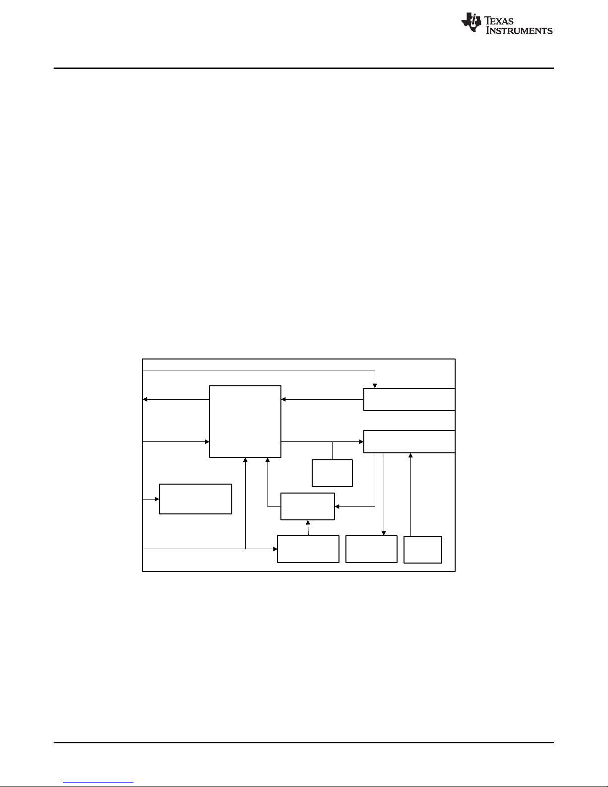
2 EVM Block Diagram
Figure 1 represents the block diagram of the ONET1131EC EVM. The board is designed to be powered
from a 2.5-V supply using cables with banana jacks.
www.ti.com
List of Tables
2
ONET1131EC Evaluation Module
Figure 1. ONET1131EC EVM Block Diagram
Copyright © 2016, Texas Instruments Incorporated
Submit Documentation Feedback
SLLU256–October 2016
Page 3
3.3-V
Power
Source for
ROSA
USB Dongle
Connector
Transmitter Inputs
Receiver Outputs
2.5-V Power
Source
www.ti.com
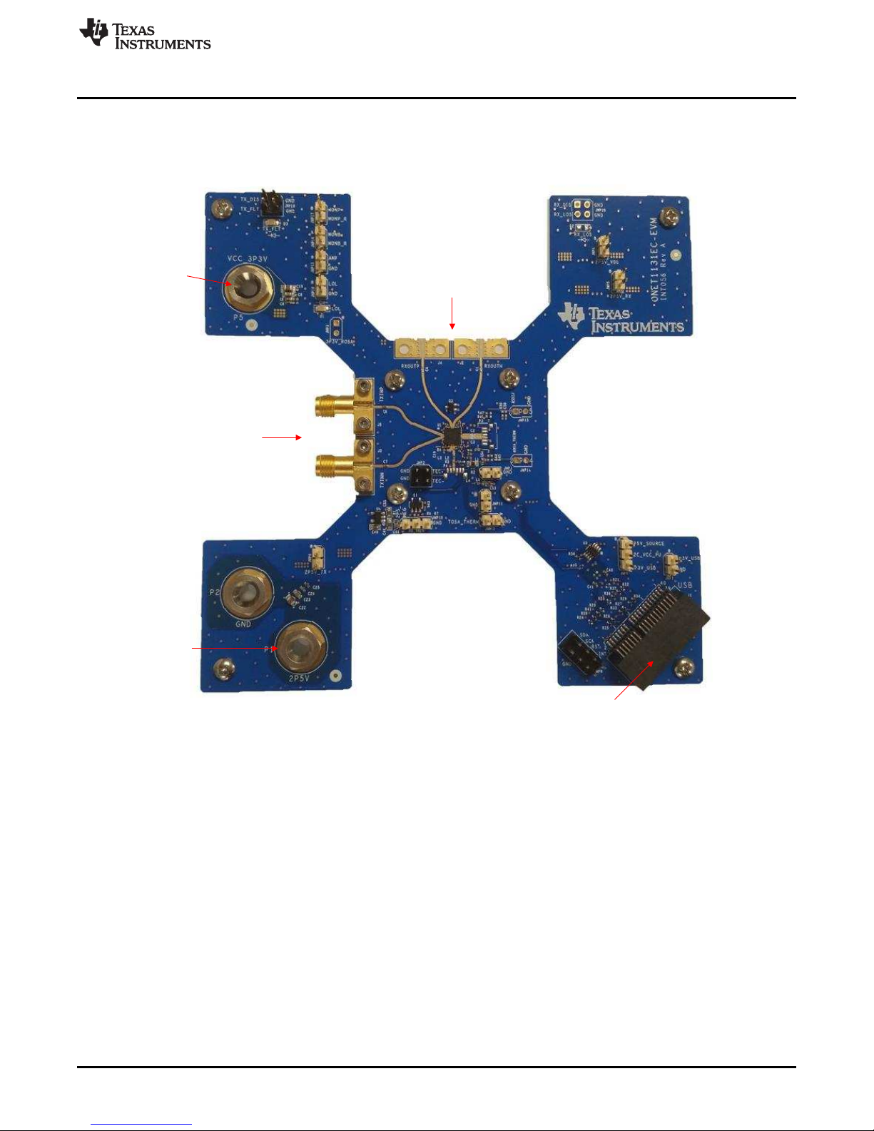
3 EVM Connections
Figure 2 shows the location of the major inputs and outputs on the EVM board.
EVM Connections
SLLU256–October 2016
Submit Documentation Feedback
Figure 2. ONET1131EC EVM Connections
Copyright © 2016, Texas Instruments Incorporated
ONET1131EC Evaluation Module
3
Page 4

TEC+
TOSA
Vea GND
Thermistor +
TECí
Thermistor í
Vea
EVM Connections
The customer must supply a ROSA and TOSA. In addition, connections for the EML bias voltage and TEC
controller are also required. Figure 3 shows the locations for the ROSA and TOSA, EML bias voltage,
TOSA thermistor, and the TEC+ and TEC– connections to the TEC controller.
www.ti.com
Figure 3. TOSA and EML Connections for TEC Controller
4
ONET1131EC Evaluation Module
Copyright © 2016, Texas Instruments Incorporated
Submit Documentation Feedback
SLLU256–October 2016
Page 5
www.ti.com
Figure 4 shows the main connections except those for the EML bias and TEC controller.
EVM Connections
ROSA and Receiver connections are not available on the ONET131EC-EVM.
SLLU256–October 2016
Submit Documentation Feedback
Figure 4. Main EVM Connections
Copyright © 2016, Texas Instruments Incorporated
ONET1131EC Evaluation Module
5
Page 6
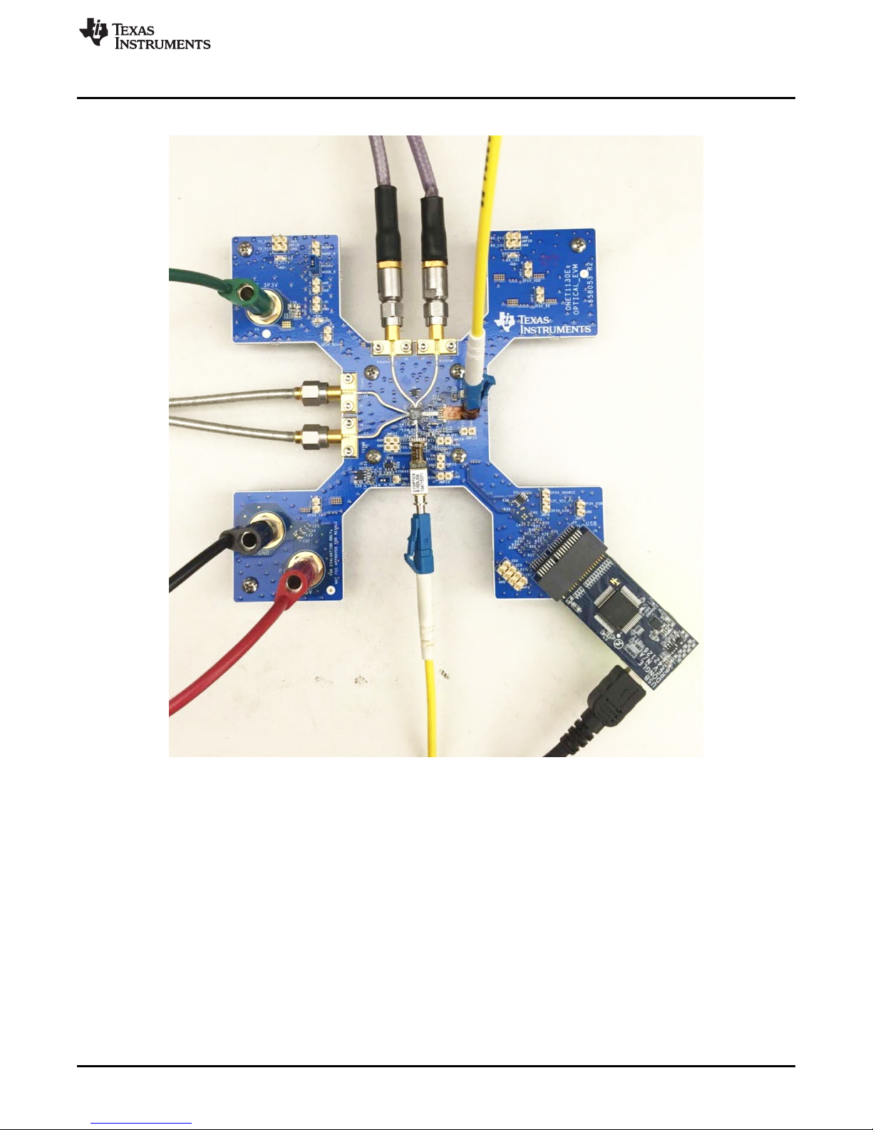
Measurement Setup
4 Measurement Setup
Follow this procedure to quickly set up to take measurements:
1. Install the ONET1130EC GUI onto the computer and follow the installation instructions.
2. Solder the TOSA onto the EVM.
3. Connect a differential data input signal source to the SMA connectors TXINP/TXINN through 50-Ω
matched impedance cables. Set the data rate between 9.8 Gbps and 11.7 Gbps. Set the amplitude
between 100 mVp-p differential and 1000 mVp-p differential.
4. Connect the USB dongle to the EVM and attach the interface cable from the USB port of the computer
to the mini-B USB port of the dongle.
5. Apply a 2.5-V supply to the +2.5-V banana jack and the supply ground to the GND banana jack.
6. Apply a negative bias voltage in the range of –0.4 V to –1.5 V for the EML to JMP28. The required
voltage is TOSA dependent.
7. Connect the TOSA thermistor at JMP24 to the TEC controller.
8. Connect the TEC+ and TEC– at JMP27 to the TEC controller.
9. Connect the TOSA to the optical input of a DCA through a single-mode fiber patch cord.
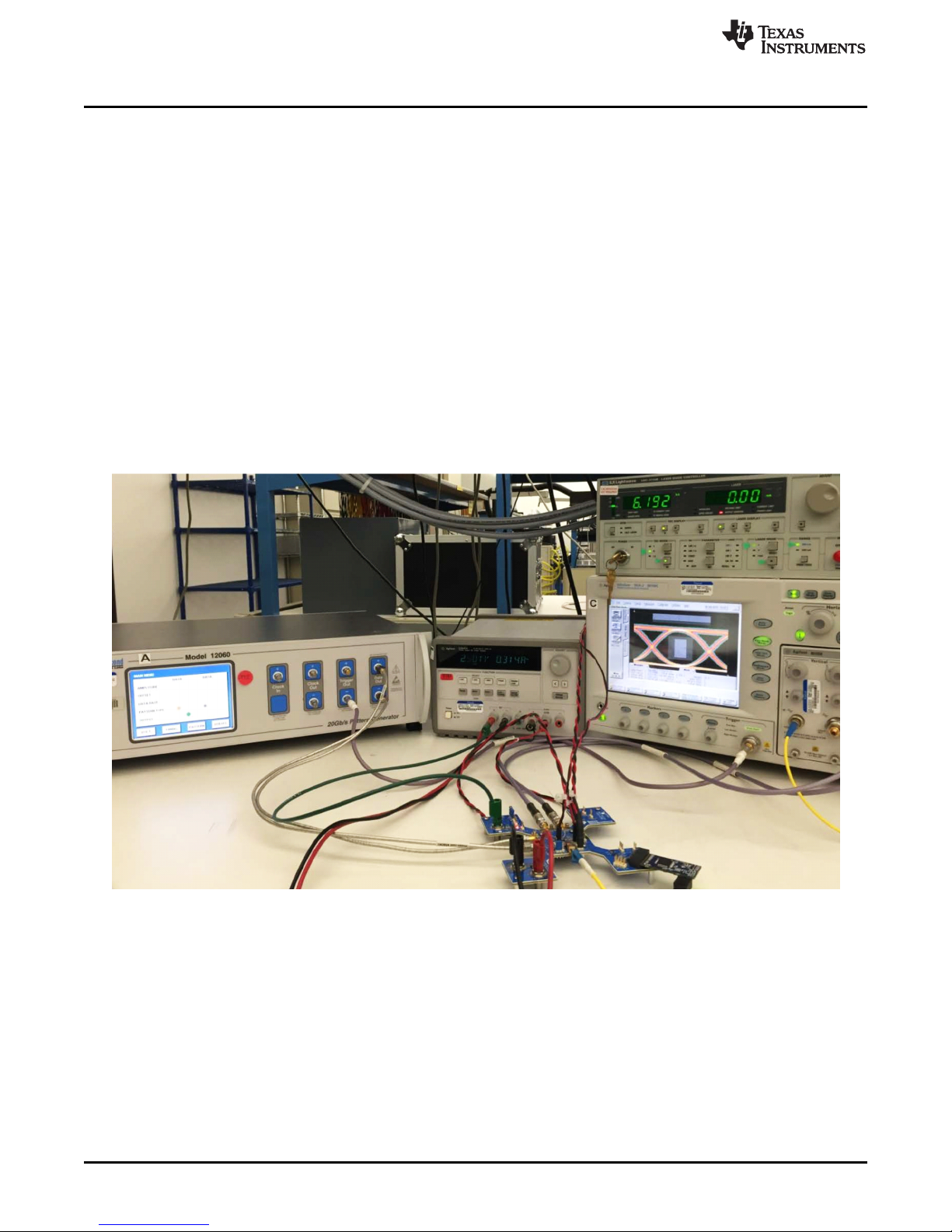
A typical setup is shown in Figure 5.
www.ti.com
6
ONET1131EC Evaluation Module
Figure 5. Typical Setup
Copyright © 2016, Texas Instruments Incorporated
Submit Documentation Feedback
SLLU256–October 2016
Page 7
www.ti.com
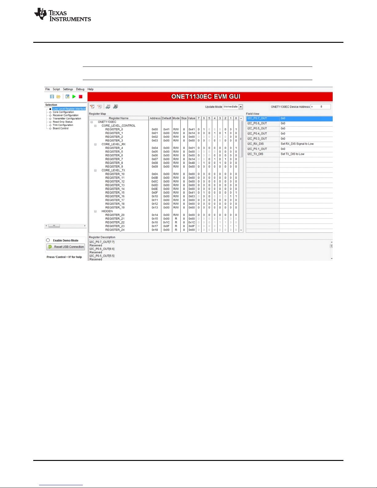
10. Run the GUI by clicking the ONET1130EC GUI shortcut icon on the desktop. The Low Level Register
Measurement Setup
Interface page appears (Figure 6).
NOTE: The ONET1130EC EVM GUI software works with the ONET1131EC EVM.
Figure 6. Low Level Register Interface Page
SLLU256–October 2016
Submit Documentation Feedback
Copyright © 2016, Texas Instruments Incorporated
ONET1131EC Evaluation Module
7
Page 8
Measurement Setup
4.1 Open Loop Operation Without Fault Detection or Digital Monitoring
The following steps are provided for open loop operation without fault detection or digital monitoring:
1. TI recommends initially operating the TOSA in open loop mode with fault detection disabled.
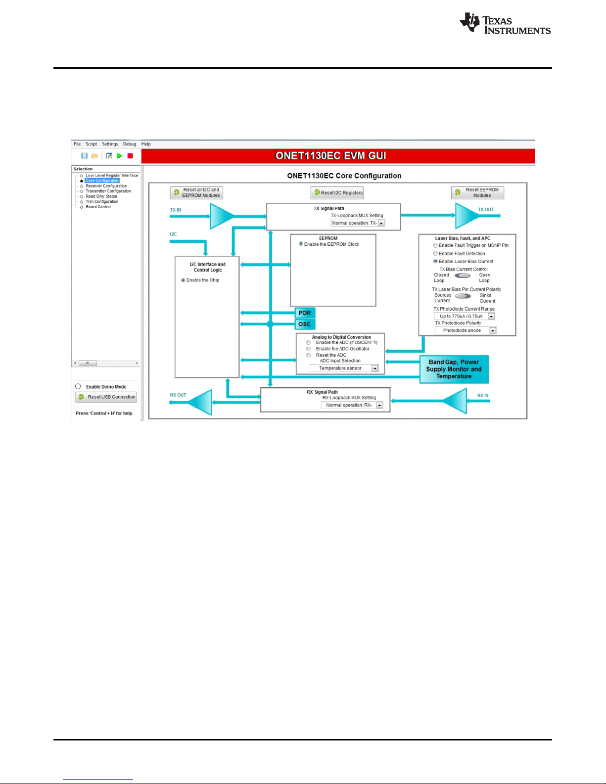
2. Go to the Core Configuration page as shown in Figure 7.
www.ti.com
Figure 7. Core Configuration Page
3. Set the TX Bias Current Control to Open Loop.
4. Enable the Laser Bias Current.
8
ONET1131EC Evaluation Module
Copyright © 2016, Texas Instruments Incorporated
Submit Documentation Feedback
SLLU256–October 2016
Page 9
www.ti.com
5. Go to the Transmitter Configuration page as shown in Figure 8.
Measurement Setup
Figure 8. Transmitter Configuration Page
6. Set TX Output Mode to Single Ended Mode (OUTP) using the pull-down box.
7. Set the desired TX Laser Bias Current with the slider.
8. Set the desired Transmitter Modulation Current with the slider.
9. Adjust the TX Cross Point with the slider.
10. If the transmitter modulation current is less than approximately 0xC0, then TI recommends using the
slow edge speed mode as selected with the TX edge speed selection bit. However, the need for using
this mode is TOSA dependent.
SLLU256–October 2016
Submit Documentation Feedback
Copyright © 2016, Texas Instruments Incorporated
ONET1131EC Evaluation Module
9
Page 10

Measurement Setup
4.2 Closed Loop Operation with Fault Detection and Digital Monitoring
The following steps are provided for closed loop operation with fault detection and digital monitoring:
1. To configure the part for automatic power control with digital monitoring and fault detection, place a
jumper between pins 1 and 2 of JMP26 to supply –2.5 V to the photodiode current mirror.
2. Go to the Core Configuration page as shown in Figure 9.
www.ti.com
Figure 9. Core Configuration Page
3. Disable the laser bias current to prevent a fault from occurring when the Fault Detection is enabled.
4. Select Enable Fault Detection and Enable the Fault Trigger on MONP Pin.
5. Set the TX Bias Current Control to Closed Loop and initially use the default 770-µA TX Photodiode
Current Range.
6. Enable the laser bias current.
7. In the Analog to Digital Conversion box, enable the ADC and ADC oscillator and select the desired
parameter to be monitored using the drop-down box.
10
ONET1131EC Evaluation Module
Copyright © 2016, Texas Instruments Incorporated
Submit Documentation Feedback
SLLU256–October 2016
Page 11

www.ti.com
8. Go to the Transmitter Configuration page as shown in Figure 10.
Measurement Setup
Figure 10. Transmitter Configuration Page
9. In the Monitor Fault Threshold box, set the Bias Current and Power sliders to their maximum value.
10. Set Digital Bias Current and Digital Photodiode Current Monitor in the Monitor Fault Threshold box.
11. Set the TX Output Mode to Single Ended Mode (OUTP).
12. Set the desired TX Laser Bias Current, Transmitter Modulation Current, and TX Cross Point (TX Eye
Cross-Point Adjust.
13. In the Monitor Fault Threshold box, reduce the Bias Current fault threshold slider until a fault occurs.
Increase the Bias Current fault threshold level at least by a value of 16.
14. Go to the Core Configuration page and toggle the Enable Laser Bias Current bit. This disables the
fault and restores the transmitter output.
15. In the Monitor Fault Threshold box, reduce the Power fault threshold slider until a fault occurs.
Increase the Power fault threshold level at least by a value of 16.
16. Go to the Core Configuration page and toggle the Enable Laser Bias Current bit. This disables the
fault and restores the transmitter output.
SLLU256–October 2016
Submit Documentation Feedback
Copyright © 2016, Texas Instruments Incorporated
ONET1131EC Evaluation Module
11
Page 12

Measurement Setup
17. To read the value from the ADC, go to the Read Only Status page as shown in Figure 11.
www.ti.com
Figure 11. Read Only Status Page
18. Click the Refresh button and read the value of the Output Representation of the ADC Input Source.
12
ONET1131EC Evaluation Module
Copyright © 2016, Texas Instruments Incorporated
Submit Documentation Feedback
SLLU256–October 2016
Page 13

www.ti.com
5 LED Indicators
Table 1 shows the meaning of the 2 LEDs on the EVM.
LED LED Color Default State Indication When On
D1 Red On The transmit CDR or the receive CDR has indicated Loss of Lock (LOL).
6 Typical Performance Results
A typical set of conditions for operating the EVM are as follows:
• 10.71 Gbps, PRBS31 Pattern
• Transmitter Single-Ended Mode of Operation
• TOSA Temperature = 37°C
• Vea = –0.65 V
• Laser Bias Current = 0xF0 (approximately 53 mA)
• Transmitter Modulation Current = 0xB0
• Transmitter Cross Point = 0xB0
• TX and RX CDRs Enabled
A typical unfiltered eye diagram is shown in Figure 12.
LED Indicators
Table 1. LED Indicators
Figure 12. Unfiltered Transmitter Eye Diagram
SLLU256–October 2016
Submit Documentation Feedback
Copyright © 2016, Texas Instruments Incorporated
ONET1131EC Evaluation Module
13
Page 14

Typical Performance Results
A typical filtered eye diagram is shown in Figure 13.
www.ti.com
Figure 13. Filtered Transmitter Eye Diagram
14
ONET1131EC Evaluation Module
Copyright © 2016, Texas Instruments Incorporated
Submit Documentation Feedback
SLLU256–October 2016
Page 15

2P5V _RX
2P5V _TX
SPLIT PLANES AND BULK DECOUPLING
3P3V _ROSA_PWR
VCC
2.5V
GND
POWER AND LOCAL DECOUPLING
Note: Isolate the VCC Nets on
either side of the Header
Pins. Connect them only
through a Wide Trace directly
between the pins on the Bottom
Layer of the Board.
2P5V _VDD
2.5V EXTERNAL INPUT
3.3V EXTERNAL INPUT
VCC
3.3V
- DNI
- DNI
2P5V_INV
VINV_C1+
VINV_C1-
2P5V_SOURCE
2P5V_SOURCE
2P5V_SOURCE
2P5V_RX
2P5V_TX
2P5V_RX
2P5V_TX
2P5V_VDD 2P5V_VDD
2P5V_TX
2P5V_RX
2P5V_SOURCE
2P5V_VDD
2P5V_SOURCE 2P5V_NEG
3P3V_SOURCE
3P3V_ROSA
3P3V_SOURCE
C24
1uF
L13
C33
100pF
C55
1uF
L11
C30
10uF
C25
0.1uF
C34
10uF
C14
0.1uF
P5
Banana-Jack
1
C6
0.1uF
R1 50
C8
1uF
C13
0.1uF
U1F
ONET1131Ex
VCC_TX1
11
VCC_TX2
14
C9
10uF
C21
0.1uF
L10
C20 DNI - 100pF
C19DNI - 0.1uF
L16
U1K
ONET1131Ex
VDD
15
C46
0.1uF
L8 JMP6
2 Pin Header
1 2
C31
1uF
C12
0.1uF
C15
22uF
C26
10uF
P1
Banana-Jack
1
JMP3
DNI - 2 Pin Header
1 2
C48
1uF
C22
22uF
C32
0.1uF
C23
10uF
L14
C37
100pF
C36
0.1uF
L15
C11
0.1uF
U1E
ONET1131Ex
VCC_RX1
27
VCC_RX2
30
C17DNI - 10uF
JMP4
2 Pin Header
1 2
JMP5
2 Pin Header
1 2
C18DNI - 1uF
C28
0.1uF
P2
Banana-Jack
1
TPS60400
U4
IN
2
OUT
1
GND
4
C1-3C1+
5
L6
C29
100pF
C27
1uF
U1G
ONET1131Ex
GND1
3
GND2
6
GND3
19
GND4
22
GND_PAD
33
C35
1uF
C49 1uF
Copyright © 2016, Texas Instruments Incorporated
www.ti.com
Schematics and Bill of Materials
15
SLLU256– October 2016
Submit Documentation Feedback
Copyright © 2016, Texas Instruments Incorporated
ONET1131EC Evaluation Module
7 Schematics and Bill of Materials
This section contains the EVM schematics and BOM.
7.1 Schematics
Figure 14, Figure 15, and Figure 16 illustrate the EVM schematics.
Figure 14. Schematic (1 of 3)
Page 16

OFFSET VOLTAGE
0201
0201
0402
0402
TXINP_SMA
TXINP
TXINN
TXINN_SMA
RXINN
RXINP
TXOUTP
RXOUTN_SMA
RXOUTP_SMA
RXOUTP
RXOUTN
VPD_IN
LD_ANODE
LD_ANODE_BT
PD_ANODE
MOD_ANODE
THERMISTOR
MOD_AN_OFFSET
TEC-
TEC+
BIAS
ROSA_PIN8
PD_ANODE_CM_E
PD_CM_E
PD_VNEG
PD
PD_CM_C
TXOUTN
ROSA_THERMISTOR
ROSA_PIN1
VPD
RXINP_ROSA
RXINN_ROSA
TXOUTP_BT
TXOUTP_BTV
MOD_AN_BT
MOD_AN_BTV
3P3V_ROSA
2P5V_NEG
2P5V_TX
2P5V_TX
R2
475
R50
DNI - 10K
DMC20201
Q1
C2
4B2C15
E2
3
E1
1
C50DNI - 0.1uF
R48
DNI - 0
JMP12
2 Pin Header
1 2
U1M
ONET1131Ex
BIAS
10
PD
7
R49 DNI_0
R6
100
L5
R3
475
C16
0.1uF
C54
0.1uF
L3
C2 DNI- 0.1uF
C51
DNI - 2.2uF
R43
0
JMP14
DNI - 2 Pin Header
1
2
L12
L9
U1A
ONET1131Ex
TXINP
4
TXINN
5
J2
DNI -sma_edge
U1B
ONET1131Ex
TXOUTN
12
TXOUTP
13
C10 0.1uFC7 0.1uF
R4
50
C1 DNI- 0.1uF
JMP15
DNI - 2 Pin Header
1
2
J3
sma_edge
JMP2
Header 2x2
132
4
R45
DNI_0
L4
L1
R47 DNI_0
C3 DNI- 0.1uF
L2
R7
100
C52
DNI - 0.1uF
EML_TOSA
P4
LD ANODE
7
PD ANODE
6
GND
5
MOD ANODE
4
GND1
3
TEC(+)
2
THERMISTOR
8
TEC(-)
1
C5 0.1uF
U1C
ONET1131Ex
RXINN
21
RXINP
20
U1D
ONET1131Ex
RXOUTN
28
RXOUTP
29
C53
0.1uF
JMP10
3 Pin Header
1
2
3
R8
475
J5
sma_edge
R5
475
ROSA
P3
VPD
7
GND2
6
DATA_N
5
DATA_P
4
GND1
3
VCC
2
GND3
8
GND
1
L7
J4
DNI -sma_edge
R46 DNI- 0
R44
DNI - 0
JMP11
2 Pin Header
1
2
C4 DNI- 0.1uF
JMP1
2 Pin Header
1
2
Copyright © 2016, Texas Instruments Incorporated
Schematics and Bill of Materials
www.ti.com
16
SLLU256– October 2016
Submit Documentation Feedback
Copyright © 2016, Texas Instruments Incorporated
ONET1131EC Evaluation Module
Figure 15. Schematic (2 of 3)
Page 17

Note: 5V_USB is not used on
this board and may show as an
open net in a DRC Check.
USB INTERFACE
I2C Monitor or External Input
I2C Pullup
Resistors already
pulled to the USB
3.3V, On-Board
resistors are
backup
DIGITAL AND I2C CONTROL
Place Q8 on the TOP side
of the board underneath
the socket as close to the
DUT as possible.
Place Q9 on the BOTTOM side
of the board underneath the
socket as close to the DUT as
possible.
Place U<x> away from
the DUT near U<x>.
I2C Device Address = 1001100
0x98 with Write Bit
0x99 with Read Bit
TEMP SENSOR
Resistors allow the I2C
to GPIO device to be
disconnected from the
ONET1131EC signals
Note: Place Loop
Filter Caps as
close to the
device pins as
possible.
ANALOG CONTROL
TX_DIS
I2C_TX_DIS
USB_I2C_SCK
USB_I2C_SDA
EXT_I2C_RESET
EXT_I2C_INT
I2C_GPIO_SDA
SDA
SCK
I2C_GPIO_SCL
USB_I2C_INT
USB_I2C_RESET
EXT_I2C_SDA
EXT_I2C_SCK
I2C_RESET
I2C_INT
I2C_ADDR
TX_FLT_L
TX_FLT_G
TX_FLT_D
I2C_RX_DIS
I2C_TX_FLT
RX_DIS
TMP_SCK
TMP_SDA
TMP_DX1
TMP_DX2
RX_LOS_L
RX_LOS_G
RX_LOS_D
TMP_DX3
TMP_DX4
RX_LOS
LOL_L
LOL_G
LOL_D
LOL
I2C_RX_LOS
I2C_LOL
TX_FLT
I2C_VCC_PU
AMP
RX_LF
TX_LF
COMP
MONP
MONB
MONP_R
MONB_R
3P3V_USB
3P3V_USB
5V_USB3P3V_USB
3P3V_USB
2P5V_SOURCE
2P5V_SOURCE
2P5V_SOURCE
2P5V_VDD
2P5V_SOURCE
3P3V_USB
2P5V_SOURCE
3P3V_USB
JMP18
2 Pin Header
1 2
R32 DNI - 0
R41
0
U2
TCA6408A_RGT
/INT
11
VCCI
15
/RESET
1
VCCP
14
GND
6
ADDR
16
SCL
12
SDA
13
P00
2
P01
3
P02
4
P03
5
P04
7
P05
8
P06
9
P07
10
GND_PP
17
JMP13
1
2
R24
DNI_10K
D2
DNI - RED
2
1
R14 0
Q3 MMSTA55
3 2
1
JMP9
Header 4x2
1
3
5
7
2
4
6
8
R40 DNI - 0
C39
1uF
R13 DNI - 0
C44
2200pF
C40
0.1uF
R21
DNI_4.99K
Q2 MMSTA55
3 2
1
JMP20
DNI - Header 2x2
132
4
R15 10K
U1L
ONET1131Ex
MONB
2
MONP
8
COMP
23
R33
0
R26 0
Q5
FDV301N
G
S
D
R51
4.99K
R37
0
R22
DNI_10K
R9
250
D3
RED
2
1
R39
0
R27 0
R31 0
R18 10K
R30 0
U1I
ONET1131Ex
RX_LOS
24
LOL/NC
1
RX_DIS
26
TX_DIS
32
TX_FLT
31
R16 DNI - 10K
R23
DNI_10K
J1A
MEC1-120-02-F-D-A Connector
1
1
3
3
5
5
7
7
9
9
11
11
13
13
17
17
19
19
21
21
23
23
25
25
27
27
29
29
31
31
33
33
35
35
37
37
39
39
C41
0.1uF
C43
0.1uF
R28
4.99K
Q4
FDV301N
G
S
D
Q6
DNI - FDV301N
G
S
D
C42
0.1uF
R350R36
0
JMP19
Header 2x2
132
4
C38
10uF
R11 250
R10
DNI - 250
JMP17
1
2
C47
0.01uF
R42 0
U1J
ONET1131Ex
RX_LF/NC
25
TX_LF/NC
9
AMP
16
R17 DNI - 10K
C45
DNI - 2200pF
R52
750
D1 RED
2
1
JMP16
1
2
R25 0
U1H
ONET1131Ex
SCK
18
SDA
17
R34
0
R38
0
R12 0
R20
DNI_10K
R29 0
U3
TMP422
DX1
1
DX2
2
DX3
3
DX44GND
5
SDA
6
SCL
7
VCC
8
R19 10K
JMP8
123
JMP7
2 Pin Header
1
2
J1B
MEC1-120-02-F-D-A Connector
2
2
4
4
6
6
8
8
10
10
12
12
14
14
18
18
20
20
22
22
24
24
26
26
28
28
30
30
32
32
34
34
36
36
38
38
40
40
Copyright © 2016, Texas Instruments Incorporated
www.ti.com
Schematics and Bill of Materials
17
SLLU256– October 2016
Submit Documentation Feedback
Copyright © 2016, Texas Instruments Incorporated
ONET1131EC Evaluation Module
Figure 16. Schematic (3 of 3)
Page 18

Schematics and Bill of Materials
www.ti.com
18
SLLU256– October 2016
Submit Documentation Feedback
Copyright © 2016, Texas Instruments Incorporated
ONET1131EC Evaluation Module
7.2 Bill of Materials
Table 2 lists the ONET1131EC EVM BOM.
Table 2. ONET1131EC EVM Bill of Materials
Item Qty Reference Value Part Number Manufacturer PCB Footprint Notes
1 1 C44 2200pF GRM033R61A222KA01D MurataElectronics North America 0201 2200pF 10V Ceramic Capacitor X5R 0201 (0603 Metric) 0.024" L x 0.012" W (0.60mm
x 0.30mm)
2 0 C45 DNI - 2200pF GRM033R61A222KA01D MurataElectronics North America 0201 2200pF 10V Ceramic Capacitor X5R 0201 (0603 Metric) 0.024" L x 0.012" W (0.60mm
x 0.30mm)
3 1 C47 0.01uF GRM033R71A103KA01D Murata Electronics North America 0201 10000pF 10V Ceramic Capacitor X7R 0201 (0603 Metric) 0.024" L x 0.012" W (0.60mm
x 0.30mm)
4 5 C11, C12, C13, C14,
C21
0.1uF GRM033R61A104KE15D MurataElectronics North America 0201 0.10µF 10V Ceramic Capacitor X5R 0201 (0603 Metric) 0.024" L x 0.012" W (0.60mm x
0.30mm))
5 3 C29, C33, C37 100pF 885012205001 Wurth Electronics Inc 0402 100pF 10V Ceramic Capacitor X7R 0402 (1005 Metric) 0.039" L x 0.020" W (1.00mm x
0.50mm)
6 0 C20 DNI - 100pF 885012205001 Wurth Electronics Inc 0402 100pF 10V Ceramic Capacitor X7R 0402 (1005 Metric) 0.039" L x 0.020" W (1.00mm x
0.50mm)
7 3 C5, C7, C10 0.1uF GRM155R71C104KA88J Murata Electronics North America 0402 0.10µF 16V Ceramic Capacitor X7R 0402 (1005 Metric) 0.039" L x 0.020" W (1.00mm x
0.50mm)
8 0 C1, C2, C3, C4, DNI- 0.1uF GRM155R71C104KA88J Murata Electronics North America 0402 0.10µF 16V Ceramic Capacitor X7R 0402 (1005 Metric) 0.039" L x 0.020" W (1.00mm x
0.50mm)
9 13 C16, C25, C28, C32,
C36, C40, C41, C42,
C43, C53, C54, C46,
C6
0.1uF GRM155R71C104KA88J Murata Electronics North America 0402 0.10µF 16V Ceramic Capacitor X7R 0402 (1005 Metric) 0.039" L x 0.020" W (1.00mm x
0.50mm)
10 0 C19, C50, C52, DNI - 0.1uF GRM155R71C104KA88J Murata Electronics North America 0402 0.10µF 16V Ceramic Capacitor X7R 0402 (1005 Metric) 0.039" L x 0.020" W (1.00mm x
0.50mm)
11 6 C24, C27, C31, C35,
C39, C8
1uF GRM155R61A105KE15D MurataElectronics North America 0402 1µF 10V Ceramic Capacitor X5R 0402 (1005 Metric) 0.039" L x 0.020" W (1.00mm x
0.50mm)
12 0 C18 DNI - 1uF GRM155R61A105KE15D MurataElectronics North America 0402 1µF 10V Ceramic Capacitor X5R 0402 (1005 Metric) 0.039" L x 0.020" W (1.00mm x
0.50mm)
13 0 C51 DNI - 2.2uF C0402C225M8PACTU Kemet 0402 2.2µF 10V Ceramic Capacitor X5R 0402 (1005 Metric) 0.039" L x 0.020" W (1.00mm x
0.50mm)
14 3 C55, C49, C48 1uF GRM188R61A105KA61D MurataElectronics North America 0603 1µF 10V Ceramic Capacitor X5R 0603 (1608 Metric) 0.063" L x 0.031" W (1.60mm x
0.80mm)
15 7 C23, C26, C30, C34,
C38, C9
10uF GRM188C81A106MA73D Murata Electronics North America 0603 10µF 10V Ceramic Capacitor X6S 0603 (1608 Metric) 0.063" L x 0.031" W (1.60mm x
0.80mm)
16 0 C17 DNI - 10uF GRM188C81A106MA73D Murata Electronics North America 0603 10µF 10V Ceramic Capacitor X6S 0603 (1608 Metric) 0.063" L x 0.031" W (1.60mm x
0.80mm)
17 2 C22, C15 22uF GRM21BR61A226ME51L Murata Electronics North America 0805 22µF 10V Ceramic Capacitor X5R 0805 (2012 Metric) 0.079" L x 0.049" W (2.00mm x
1.25mm)
18 4 R5, R8, R3, R2 475 ERJ-1GEF4750C Panasonic Electronic Components 0201 RES SMD 475 OHM 1% 1/20W 0201
19 18 R12,R14, R25, R26,
R27, R29, R30, R31,
R33, R34, R35, R36,
R37, R38, R39, R41,
R42, R43
0 RC0402JR-070RL Yageo 0402 RES SMD 0.0OHM JUMPER 1/16W 0402
20 0 R13, R32, R40, R48,
R46, R44
DNI - 0 RC0402JR-070RL Yageo 0402 RES SMD 0.0OHM JUMPER 1/16W 0402
21 0 R49, R47, R45 DNI_0 Any (1% Tolerance) Any 0402
22 2 R4, R1 50 504L50R0FTNCFT American Technical Ceramics 0402 RES SMD 50 OHM 1% 1/8W 0402
Page 19

www.ti.com
Schematics and Bill of Materials
19
SLLU256– October 2016
Submit Documentation Feedback
Copyright © 2016, Texas Instruments Incorporated
ONET1131EC Evaluation Module
Table 2. ONET1131EC EVM Bill of Materials (continued)
Item Qty Reference Value Part Number Manufacturer PCB Footprint Notes
23 2 R7, R6 100 RC0402FR-07100RL Yageo 0402 RES SMD 100 OHM 1% 1/16W 0402
24 3 R9, R11 249 RC0402FR-07249RL Yageo 0402 RES SMD 249 OHM 1% 1/16W 0402
25 0 R10 DNI - 249 RC0402FR-07249RL Yageo 0402 RES SMD 249 OHM 1% 1/16W 0402
26 1 R28 4.99K ERJ-2RKF4991X Panasonic Electronic Components 0402 RES SMD 4.99K OHM 1% 1/10W 0402
27 0 R21 DNI_4.99K Any (1% Tolerance) Any 0402
28 6 R15, R18, R19 10K RC0402JR-0710KL Yageo 0402 RES SMD 10K OHM 5% 1/16W 0402
29 0 R16, R17, R50 DNI - 10K RC0402JR-0710KL Yageo 0402 RES SMD 10K OHM 5% 1/16W 0402
30 0 R20, R22, R23, R24 DNI_10K Any (1% Tolerance) Any 0402
31 1 R52 750 RC0805JR-07750RL Yageo 0805 RES SMD 750 OHM 5% 1/8W 0805
32 1 R51 4.99K ERJ-6ENF4991V Panasonic Electronic Components 0805 RES SMD 4.99K OHM 1% 1/8W 0805
33 3 D1, D3 RED HSMS-C170 Avago Technologies Us Inc LED_SM_HSMB_C170 Red 626nm LED Indication Discrete 2.1V Diffused White Lens 0805 (2012 Metric)
34 0 D2 DNI - RED HSMS-C170 Avago Technologies Us Inc LED_SM_HSMB_C170 Red 626nm LED Indication Discrete 2.1V Diffused White Lens 0805 (2012 Metric)
35 11 JMP4,JMP5, JMP6,
JMP7, JMP13,
JMP16, JMP17,
JMP18, JMP12,
JMP11, JMP1
0.1" Header (1x2) TSW-150-08-G-S Samtec HDR_THVT_1x2_100 50 Positions Header, Unshrouded Connector 0.100" (2.54mm) Through Hole Gold
36 0 JMP3, JMP15,
JMP14,
DNI - 0.1" Header
(1x2)
TSW-150-08-G-S Samtec HDR_THVT_1x2_100 50 Positions Header, Unshrouded Connector 0.100" (2.54mm) Through Hole Gold
37 2 JMP8, JMP10 0.1" Header (1x3) TSW-150-08-G-S Samtec HDR_THVT_1X3_100 50 Positions Header, Unshrouded Connector 0.100" (2.54mm) Through Hole Gold
38 2 JMP19, JMP2 0.1x0.1" Header (2x2) 67997-404HLF Amphenol HDR_THVT_2x2_100 4 Positions Header, Unshrouded Connector 0.100" (2.54mm) Through Hole Tin
39 0 JMP20 DNI - 0.1x0.1" Header
(2x2)
67997-404HLF Amphenol HDR_THVT_2x2_100 4 Positions Header, Unshrouded Connector 0.100" (2.54mm) Through Hole Tin
40 1 JMP9 0.1x0.1" Header (2x4) TSW-150-08-G-S Samtec HDR_THVT_2X4_100 50 Positions Header, Unshrouded Connector 0.100" (2.54mm) Through Hole Gold
41 2 J5, J3 Edge Launch SMA 32K243-40ML5 Rosenberger CON_02K243-40M RF Connectors / Coaxial Connectors R/A Jack PCB
42 0 J2, J4, DNI - Edge Launch
SMA
32K243-40ML5 Rosenberger CON_02K243-40M RF Connectors / Coaxial Connectors R/A Jack PCB
43 1 J1 MEC1-120-02-F-D-A
Connector
MEC1-120-02-F-D-RA1-SL Samtec CON_SMRT_MEC1_4
0_F
CONN EDGE CARD DL 40POS SMD
44 2 L12, L1 Inductor 47uH, 35mA GLFR1608T470M-LR Taiyo Yuden 0603 47µH Shielded Wirewound Inductor 100mA 2.3 Ohm 0603 (1608 Metric)
45 3 L9, L5, L2 Ferrite Bead 1.8kohm,
200mA
BLM15HD182SN1D Murata 0402_2020MIL 1.8kOhm Impedance Ferrite Bead 0402 (1005 Metric) Surface Mount Signal Line
200mA 1 Lines 2.2 Ohm Max DCR -55°C ~ 125°C
46 3 L7, L4, L3 Ferrite Bead 1000ohm,
125mA
BLM03HG102SN1D MuRata 0201 1 kOhm Impedance Ferrite Bead 0201 (0603 Metric) Surface Mount 125mA 1 Lines 2.6
Ohm Max DCR -55°C ~ 125°C
47 3 L15, L11, L8 CIC10P330 CIC10P330 Samsung 0603 33 Ohm Impedance Ferrite Bead 0603 (1608 Metric) Surface Mount Power Line 3A 1
Lines 25 mOhm Max DCR -55°C ~ 125°C
48 0 L13 DNI - CIC10P330 CIC10P330 Samsung 0603 33 Ohm Impedance Ferrite Bead 0603 (1608 Metric) Surface Mount Power Line 3A 1
Lines 25 mOhm Max DCR -55°C ~ 125°C
49 4 L16, L10, L6 DNI_CIC10P330 CIC10P330 Samsung 0603 33 Ohm Impedance Ferrite Bead 0603 (1608 Metric) Surface Mount Power Line 3A 1
Lines 25 mOhm Max DCR -55°C ~ 125°C
50 0 L14, DNI_CIC10P330 CIC10P330 Samsung 0603 33 Ohm Impedance Ferrite Bead 0603 (1608 Metric) Surface Mount Power Line 3A 1
Lines 25 mOhm Max DCR -55°C ~ 125°C
51 3 P1, P2, P5 Solderless Banana
Jack
108-0740-001 Emerson Network Power JACK_THVT_BANANA
_500dia
Banana Jack Connector Standard Banana Threaded, External (Nut)
52 0 P3 DNI_ROSA DNI DNI MSA_XMD_ROSA_INVNote: TI will assemble the ROSA
Page 20

Schematics and Bill of Materials
www.ti.com
20
SLLU256– October 2016
Submit Documentation Feedback
Copyright © 2016, Texas Instruments Incorporated
ONET1131EC Evaluation Module
Table 2. ONET1131EC EVM Bill of Materials (continued)
Item Qty Reference Value Part Number Manufacturer PCB Footprint Notes
53 0 P4 DNI_EML_TOSA DNI DNI 162X_TOSA Note: TI will assemble the TOSA
54 3 Q5, Q4 FDV301N FDV301N Fairchild SOT23_3 MOSFET N-CH 25V 220MA SOT-23
55 0 Q6, DNI - FDV301N FDV301N Fairchild SOT23_3 MOSFET N-CH 25V 220MA SOT-23
56 2 Q3, Q2 MMSTA55 MMSTA55-7-F Diodes Inc. SOT_323-3 TRANS PNP 60V 0.5A SC70-3
57 1 Q1 DMC20201 DMC20201 Panasonic SOT23_5 TRANS 2NPN 50V 0.1A MINI5
58 1 U1 ONET1131Ex ONET1131ECRSMT Texas Instruments ONET1130Ex_QFN32 Note: TI will supply
59 1 U2 TCA6408A_RGT TCA6408ARGTR Texas Instruments QFN_16_3MSQ IC I/O EXPANDER I2C 8B 16QFN
60 1 U3 TMP422 TMP422AIDCNT Texas Instruments DCN_SOT23-8 SENSORTEMPERATURE SMBUS SOT23-8
61 1 U4 TPS60400 TPS60400DBVT Texas Instruments SOT23-5 Charge Pump Switching Regulator IC Positive or Negative Fixed -Vin, 2Vin, Vin/2 1
Output 60mA SC-74A, SOT-753
62 8 Standoff Round Threaded 0.5" 2204 Keystone Electronics ROUND SPACER #4 NYLON 1/2"
63 8 Screws Round 4-40/0.25" PMSSS 440 0025 PH Building Fasteners PMSSS 440 0025 PH
64 1 PCB ONET1131EC-EVM INT056 ANY PCB boards
Page 21

STANDARD TERMS AND CONDITIONS FOR EVALUATION MODULES
1. Delivery: TI delivers TI evaluation boards, kits, or modules, including any accompanying demonstration software, components, or
documentation (collectively, an “EVM” or “EVMs”) to the User (“User”) in accordance with the terms and conditions set forth herein.
Acceptance of the EVM is expressly subject to the following terms and conditions.
1.1 EVMs are intended solely for product or software developers for use in a research and development setting to facilitate feasibility
evaluation, experimentation, or scientific analysis of TI semiconductors products. EVMs have no direct function and are not
finished products. EVMs shall not be directly or indirectly assembled as a part or subassembly in any finished product. For
clarification, any software or software tools provided with the EVM (“Software”) shall not be subject to the terms and conditions
set forth herein but rather shall be subject to the applicable terms and conditions that accompany such Software
1.2 EVMs are not intended for consumer or household use. EVMs may not be sold, sublicensed, leased, rented, loaned, assigned,
or otherwise distributed for commercial purposes by Users, in whole or in part, or used in any finished product or production
system.
2 Limited Warranty and Related Remedies/Disclaimers:
2.1 These terms and conditions do not apply to Software. The warranty, if any, for Software is covered in the applicable Software
License Agreement.
2.2 TI warrants that the TI EVM will conform to TI's published specifications for ninety (90) days after the date TI delivers such EVM
to User. Notwithstanding the foregoing, TI shall not be liable for any defects that are caused by neglect, misuse or mistreatment
by an entity other than TI, including improper installation or testing, or for any EVMs that have been altered or modified in any
way by an entity other than TI. Moreover, TI shall not be liable for any defects that result from User's design, specifications or
instructions for such EVMs. Testing and other quality control techniques are used to the extent TI deems necessary or as
mandated by government requirements. TI does not test all parameters of each EVM.
2.3 If any EVM fails to conform to the warranty set forth above, TI's sole liability shall be at its option to repair or replace such EVM,
or credit User's account for such EVM. TI's liability under this warranty shall be limited to EVMs that are returned during the
warranty period to the address designated by TI and that are determined by TI not to conform to such warranty. If TI elects to
repair or replace such EVM, TI shall have a reasonable time to repair such EVM or provide replacements. Repaired EVMs shall
be warranted for the remainder of the original warranty period. Replaced EVMs shall be warranted for a new full ninety (90) day
warranty period.
3 Regulatory Notices:
3.1 United States
3.1.1 Notice applicable to EVMs not FCC-Approved:
This kit is designed to allow product developers to evaluate electronic components, circuitry, or software associated with the kit
to determine whether to incorporate such items in a finished product and software developers to write software applications for
use with the end product. This kit is not a finished product and when assembled may not be resold or otherwise marketed unless
all required FCC equipment authorizations are first obtained. Operation is subject to the condition that this product not cause
harmful interference to licensed radio stations and that this product accept harmful interference. Unless the assembled kit is
designed to operate under part 15, part 18 or part 95 of this chapter, the operator of the kit must operate under the authority of
an FCC license holder or must secure an experimental authorization under part 5 of this chapter.
3.1.2 For EVMs annotated as FCC – FEDERAL COMMUNICATIONS COMMISSION Part 15 Compliant:
CAUTION
This device complies with part 15 of the FCC Rules. Operation is subject to the following two conditions: (1) This device may not
cause harmful interference, and (2) this device must accept any interference received, including interference that may cause
undesired operation.
Changes or modifications not expressly approved by the party responsible for compliance could void the user's authority to
operate the equipment.
FCC Interference Statement for Class A EVM devices
NOTE: This equipment has been tested and found to comply with the limits for a Class A digital device, pursuant to part 15 of
the FCC Rules. These limits are designed to provide reasonable protection against harmful interference when the equipment is
operated in a commercial environment. This equipment generates, uses, and can radiate radio frequency energy and, if not
installed and used in accordance with the instruction manual, may cause harmful interference to radio communications.
Operation of this equipment in a residential area is likely to cause harmful interference in which case the user will be required to
correct the interference at his own expense.
SPACER
SPACER
SPACER
SPACER
SPACER
SPACER
SPACER
SPACER
Page 22

FCC Interference Statement for Class B EVM devices
NOTE: This equipment has been tested and found to comply with the limits for a Class B digital device, pursuant to part 15 of
the FCC Rules. These limits are designed to provide reasonable protection against harmful interference in a residential
installation. This equipment generates, uses and can radiate radio frequency energy and, if not installed and used in accordance
with the instructions, may cause harmful interference to radio communications. However, there is no guarantee that interference
will not occur in a particular installation. If this equipment does cause harmful interference to radio or television reception, which
can be determined by turning the equipment off and on, the user is encouraged to try to correct the interference by one or more
of the following measures:
• Reorient or relocate the receiving antenna.
• Increase the separation between the equipment and receiver.
• Connect the equipment into an outlet on a circuit different from that to which the receiver is connected.
• Consult the dealer or an experienced radio/TV technician for help.
3.2 Canada
3.2.1 For EVMs issued with an Industry Canada Certificate of Conformance to RSS-210
Concerning EVMs Including Radio Transmitters:
This device complies with Industry Canada license-exempt RSS standard(s). Operation is subject to the following two conditions:
(1) this device may not cause interference, and (2) this device must accept any interference, including interference that may
cause undesired operation of the device.
Concernant les EVMs avec appareils radio:
Le présent appareil est conforme aux CNR d'Industrie Canada applicables aux appareils radio exempts de licence. L'exploitation
est autorisée aux deux conditions suivantes: (1) l'appareil ne doit pas produire de brouillage, et (2) l'utilisateur de l'appareil doit
accepter tout brouillage radioélectrique subi, même si le brouillage est susceptible d'en compromettre le fonctionnement.
Concerning EVMs Including Detachable Antennas:
Under Industry Canada regulations, this radio transmitter may only operate using an antenna of a type and maximum (or lesser)
gain approved for the transmitter by Industry Canada. To reduce potential radio interference to other users, the antenna type
and its gain should be so chosen that the equivalent isotropically radiated power (e.i.r.p.) is not more than that necessary for
successful communication. This radio transmitter has been approved by Industry Canada to operate with the antenna types
listed in the user guide with the maximum permissible gain and required antenna impedance for each antenna type indicated.
Antenna types not included in this list, having a gain greater than the maximum gain indicated for that type, are strictly prohibited
for use with this device.
Concernant les EVMs avec antennes détachables
Conformément à la réglementation d'Industrie Canada, le présent émetteur radio peut fonctionner avec une antenne d'un type et
d'un gain maximal (ou inférieur) approuvé pour l'émetteur par Industrie Canada. Dans le but de réduire les risques de brouillage
radioélectrique à l'intention des autres utilisateurs, il faut choisir le type d'antenne et son gain de sorte que la puissance isotrope
rayonnée équivalente (p.i.r.e.) ne dépasse pas l'intensité nécessaire à l'établissement d'une communication satisfaisante. Le
présent émetteur radio a été approuvé par Industrie Canada pour fonctionner avec les types d'antenne énumérés dans le
manuel d’usage et ayant un gain admissible maximal et l'impédance requise pour chaque type d'antenne. Les types d'antenne
non inclus dans cette liste, ou dont le gain est supérieur au gain maximal indiqué, sont strictement interdits pour l'exploitation de
l'émetteur
3.3 Japan
3.3.1 Notice for EVMs delivered in Japan: Please see http://www.tij.co.jp/lsds/ti_ja/general/eStore/notice_01.page 日本国内に
輸入される評価用キット、ボードについては、次のところをご覧ください。
http://www.tij.co.jp/lsds/ti_ja/general/eStore/notice_01.page
3.3.2 Notice for Users of EVMs Considered “Radio Frequency Products” in Japan: EVMs entering Japan may not be certified
by TI as conforming to Technical Regulations of Radio Law of Japan.
If User uses EVMs in Japan, not certified to Technical Regulations of Radio Law of Japan, User is required by Radio Law of
Japan to follow the instructions below with respect to EVMs:
1. Use EVMs in a shielded room or any other test facility as defined in the notification #173 issued by Ministry of Internal
Affairs and Communications on March 28, 2006, based on Sub-section 1.1 of Article 6 of the Ministry’s Rule for
Enforcement of Radio Law of Japan,
2. Use EVMs only after User obtains the license of Test Radio Station as provided in Radio Law of Japan with respect to
EVMs, or
3. Use of EVMs only after User obtains the Technical Regulations Conformity Certification as provided in Radio Law of Japan
with respect to EVMs. Also, do not transfer EVMs, unless User gives the same notice above to the transferee. Please note
that if User does not follow the instructions above, User will be subject to penalties of Radio Law of Japan.
SPACER
SPACER
SPACER
SPACER
SPACER
Page 23

【無線電波を送信する製品の開発キットをお使いになる際の注意事項】 開発キットの中には技術基準適合証明を受けて
いないものがあります。 技術適合証明を受けていないもののご使用に際しては、電波法遵守のため、以下のいずれかの
措置を取っていただく必要がありますのでご注意ください。
1. 電波法施行規則第6条第1項第1号に基づく平成18年3月28日総務省告示第173号で定められた電波暗室等の試験設備でご使用
いただく。
2. 実験局の免許を取得後ご使用いただく。
3. 技術基準適合証明を取得後ご使用いただく。
なお、本製品は、上記の「ご使用にあたっての注意」を譲渡先、移転先に通知しない限り、譲渡、移転できないものとします。
上記を遵守頂けない場合は、電波法の罰則が適用される可能性があることをご留意ください。 日本テキサス・イ
ンスツルメンツ株式会社
東京都新宿区西新宿6丁目24番1号
西新宿三井ビル
3.3.3 Notice for EVMs for Power Line Communication: Please see http://www.tij.co.jp/lsds/ti_ja/general/eStore/notice_02.page
電力線搬送波通信についての開発キットをお使いになる際の注意事項については、次のところをご覧くださ
い。http://www.tij.co.jp/lsds/ti_ja/general/eStore/notice_02.page
SPACER
4 EVM Use Restrictions and Warnings:
4.1 EVMS ARE NOT FOR USE IN FUNCTIONAL SAFETY AND/OR SAFETY CRITICAL EVALUATIONS, INCLUDING BUT NOT
LIMITED TO EVALUATIONS OF LIFE SUPPORT APPLICATIONS.
4.2 User must read and apply the user guide and other available documentation provided by TI regarding the EVM prior to handling
or using the EVM, including without limitation any warning or restriction notices. The notices contain important safety information
related to, for example, temperatures and voltages.
4.3 Safety-Related Warnings and Restrictions:
4.3.1 User shall operate the EVM within TI’s recommended specifications and environmental considerations stated in the user
guide, other available documentation provided by TI, and any other applicable requirements and employ reasonable and
customary safeguards. Exceeding the specified performance ratings and specifications (including but not limited to input
and output voltage, current, power, and environmental ranges) for the EVM may cause personal injury or death, or
property damage. If there are questions concerning performance ratings and specifications, User should contact a TI
field representative prior to connecting interface electronics including input power and intended loads. Any loads applied
outside of the specified output range may also result in unintended and/or inaccurate operation and/or possible
permanent damage to the EVM and/or interface electronics. Please consult the EVM user guide prior to connecting any
load to the EVM output. If there is uncertainty as to the load specification, please contact a TI field representative.
During normal operation, even with the inputs and outputs kept within the specified allowable ranges, some circuit
components may have elevated case temperatures. These components include but are not limited to linear regulators,
switching transistors, pass transistors, current sense resistors, and heat sinks, which can be identified using the
information in the associated documentation. When working with the EVM, please be aware that the EVM may become
very warm.
4.3.2 EVMs are intended solely for use by technically qualified, professional electronics experts who are familiar with the
dangers and application risks associated with handling electrical mechanical components, systems, and subsystems.
User assumes all responsibility and liability for proper and safe handling and use of the EVM by User or its employees,
affiliates, contractors or designees. User assumes all responsibility and liability to ensure that any interfaces (electronic
and/or mechanical) between the EVM and any human body are designed with suitable isolation and means to safely
limit accessible leakage currents to minimize the risk of electrical shock hazard. User assumes all responsibility and
liability for any improper or unsafe handling or use of the EVM by User or its employees, affiliates, contractors or
designees.
4.4 User assumes all responsibility and liability to determine whether the EVM is subject to any applicable international, federal,
state, or local laws and regulations related to User’s handling and use of the EVM and, if applicable, User assumes all
responsibility and liability for compliance in all respects with such laws and regulations. User assumes all responsibility and
liability for proper disposal and recycling of the EVM consistent with all applicable international, federal, state, and local
requirements.
5. Accuracy of Information: To the extent TI provides information on the availability and function of EVMs, TI attempts to be as accurate
as possible. However, TI does not warrant the accuracy of EVM descriptions, EVM availability or other information on its websites as
accurate, complete, reliable, current, or error-free.
SPACER
SPACER
SPACER
SPACER
SPACER
SPACER
Page 24

SPACER
6. Disclaimers:
6.1 EXCEPT AS SET FORTH ABOVE, EVMS AND ANY WRITTEN DESIGN MATERIALS PROVIDED WITH THE EVM (AND THE
DESIGN OF THE EVM ITSELF) ARE PROVIDED "AS IS" AND "WITH ALL FAULTS." TI DISCLAIMS ALL OTHER
WARRANTIES, EXPRESS OR IMPLIED, REGARDING SUCH ITEMS, INCLUDING BUT NOT LIMITED TO ANY IMPLIED
WARRANTIES OF MERCHANTABILITY OR FITNESS FOR A PARTICULAR PURPOSE OR NON-INFRINGEMENT OF ANY
THIRD PARTY PATENTS, COPYRIGHTS, TRADE SECRETS OR OTHER INTELLECTUAL PROPERTY RIGHTS.
6.2 EXCEPT FOR THE LIMITED RIGHT TO USE THE EVM SET FORTH HEREIN, NOTHING IN THESE TERMS AND
CONDITIONS SHALL BE CONSTRUED AS GRANTING OR CONFERRING ANY RIGHTS BY LICENSE, PATENT, OR ANY
OTHER INDUSTRIAL OR INTELLECTUAL PROPERTY RIGHT OF TI, ITS SUPPLIERS/LICENSORS OR ANY OTHER THIRD
PARTY, TO USE THE EVM IN ANY FINISHED END-USER OR READY-TO-USE FINAL PRODUCT, OR FOR ANY
INVENTION, DISCOVERY OR IMPROVEMENT MADE, CONCEIVED OR ACQUIRED PRIOR TO OR AFTER DELIVERY OF
THE EVM.
7. USER'S INDEMNITY OBLIGATIONS AND REPRESENTATIONS. USER WILL DEFEND, INDEMNIFY AND HOLD TI, ITS
LICENSORS AND THEIR REPRESENTATIVES HARMLESS FROM AND AGAINST ANY AND ALL CLAIMS, DAMAGES, LOSSES,
EXPENSES, COSTS AND LIABILITIES (COLLECTIVELY, "CLAIMS") ARISING OUT OF OR IN CONNECTION WITH ANY
HANDLING OR USE OF THE EVM THAT IS NOT IN ACCORDANCE WITH THESE TERMS AND CONDITIONS. THIS OBLIGATION
SHALL APPLY WHETHER CLAIMS ARISE UNDER STATUTE, REGULATION, OR THE LAW OF TORT, CONTRACT OR ANY
OTHER LEGAL THEORY, AND EVEN IF THE EVM FAILS TO PERFORM AS DESCRIBED OR EXPECTED.
8. Limitations on Damages and Liability:
8.1 General Limitations. IN NO EVENT SHALL TI BE LIABLE FOR ANY SPECIAL, COLLATERAL, INDIRECT, PUNITIVE,
INCIDENTAL, CONSEQUENTIAL, OR EXEMPLARY DAMAGES IN CONNECTION WITH OR ARISING OUT OF THESE
TERMS ANDCONDITIONS OR THE USE OF THE EVMS PROVIDED HEREUNDER, REGARDLESS OF WHETHER TI HAS
BEEN ADVISED OF THE POSSIBILITY OF SUCH DAMAGES. EXCLUDED DAMAGES INCLUDE, BUT ARE NOT LIMITED
TO, COST OF REMOVAL OR REINSTALLATION, ANCILLARY COSTS TO THE PROCUREMENT OF SUBSTITUTE GOODS
OR SERVICES, RETESTING, OUTSIDE COMPUTER TIME, LABOR COSTS, LOSS OF GOODWILL, LOSS OF PROFITS,
LOSS OF SAVINGS, LOSS OF USE, LOSS OF DATA, OR BUSINESS INTERRUPTION. NO CLAIM, SUIT OR ACTION SHALL
BE BROUGHT AGAINST TI MORE THAN ONE YEAR AFTER THE RELATED CAUSE OF ACTION HAS OCCURRED.
8.2 Specific Limitations. IN NO EVENT SHALL TI'S AGGREGATE LIABILITY FROM ANY WARRANTY OR OTHER OBLIGATION
ARISING OUT OF OR IN CONNECTION WITH THESE TERMS AND CONDITIONS, OR ANY USE OF ANY TI EVM
PROVIDED HEREUNDER, EXCEED THE TOTAL AMOUNT PAID TO TI FOR THE PARTICULAR UNITS SOLD UNDER
THESE TERMS AND CONDITIONS WITH RESPECT TO WHICH LOSSES OR DAMAGES ARE CLAIMED. THE EXISTENCE
OF MORE THAN ONE CLAIM AGAINST THE PARTICULAR UNITS SOLD TO USER UNDER THESE TERMS AND
CONDITIONS SHALL NOT ENLARGE OR EXTEND THIS LIMIT.
9. Return Policy. Except as otherwise provided, TI does not offer any refunds, returns, or exchanges. Furthermore, no return of EVM(s)
will be accepted if the package has been opened and no return of the EVM(s) will be accepted if they are damaged or otherwise not in
a resalable condition. If User feels it has been incorrectly charged for the EVM(s) it ordered or that delivery violates the applicable
order, User should contact TI. All refunds will be made in full within thirty (30) working days from the return of the components(s),
excluding any postage or packaging costs.
10. Governing Law: These terms and conditions shall be governed by and interpreted in accordance with the laws of the State of Texas,
without reference to conflict-of-laws principles. User agrees that non-exclusive jurisdiction for any dispute arising out of or relating to
these terms and conditions lies within courts located in the State of Texas and consents to venue in Dallas County, Texas.
Notwithstanding the foregoing, any judgment may be enforced in any United States or foreign court, and TI may seek injunctive relief
in any United States or foreign court.
Mailing Address: Texas Instruments, Post Office Box 655303, Dallas, Texas 75265
spacer
Copyright © 2015, Texas Instruments Incorporated
Page 25

STANDARD TERMS FOR EVALUATION MODULES
1. Delivery: TI delivers TI evaluation boards, kits, or modules, including any accompanying demonstration software, components, and/or
documentation which may be provided together or separately (collectively, an “EVM” or “EVMs”) to the User (“User”) in accordance
with the terms set forth herein. User's acceptance of the EVM is expressly subject to the following terms.
1.1 EVMs are intended solely for product or software developers for use in a research and development setting to facilitate feasibility
evaluation, experimentation, or scientific analysis of TI semiconductors products. EVMs have no direct function and are not
finished products. EVMs shall not be directly or indirectly assembled as a part or subassembly in any finished product. For
clarification, any software or software tools provided with the EVM (“Software”) shall not be subject to the terms and conditions
set forth herein but rather shall be subject to the applicable terms that accompany such Software
1.2 EVMs are not intended for consumer or household use. EVMs may not be sold, sublicensed, leased, rented, loaned, assigned,
or otherwise distributed for commercial purposes by Users, in whole or in part, or used in any finished product or production
system.
2 Limited Warranty and Related Remedies/Disclaimers:
2.1 These terms do not apply to Software. The warranty, if any, for Software is covered in the applicable Software License
Agreement.
2.2 TI warrants that the TI EVM will conform to TI's published specifications for ninety (90) days after the date TI delivers such EVM
to User. Notwithstanding the foregoing, TI shall not be liable for a nonconforming EVM if (a) the nonconformity was caused by
neglect, misuse or mistreatment by an entity other than TI, including improper installation or testing, or for any EVMs that have
been altered or modified in any way by an entity other than TI, (b) the nonconformity resulted from User's design, specifications
or instructions for such EVMs or improper system design, or (c) User has not paid on time. Testing and other quality control
techniques are used to the extent TI deems necessary. TI does not test all parameters of each EVM.
User's claims against TI under this Section 2 are void if User fails to notify TI of any apparent defects in the EVMs within ten (10)
business days after delivery, or of any hidden defects with ten (10) business days after the defect has been detected.
2.3 TI's sole liability shall be at its option to repair or replace EVMs that fail to conform to the warranty set forth above, or credit
User's account for such EVM. TI's liability under this warranty shall be limited to EVMs that are returned during the warranty
period to the address designated by TI and that are determined by TI not to conform to such warranty. If TI elects to repair or
replace such EVM, TI shall have a reasonable time to repair such EVM or provide replacements. Repaired EVMs shall be
warranted for the remainder of the original warranty period. Replaced EVMs shall be warranted for a new full ninety (90) day
warranty period.
3 Regulatory Notices:
3.1 United States
3.1.1 Notice applicable to EVMs not FCC-Approved:
FCC NOTICE: This kit is designed to allow product developers to evaluate electronic components, circuitry, or software
associated with the kit to determine whether to incorporate such items in a finished product and software developers to write
software applications for use with the end product. This kit is not a finished product and when assembled may not be resold or
otherwise marketed unless all required FCC equipment authorizations are first obtained. Operation is subject to the condition
that this product not cause harmful interference to licensed radio stations and that this product accept harmful interference.
Unless the assembled kit is designed to operate under part 15, part 18 or part 95 of this chapter, the operator of the kit must
operate under the authority of an FCC license holder or must secure an experimental authorization under part 5 of this chapter.
3.1.2 For EVMs annotated as FCC – FEDERAL COMMUNICATIONS COMMISSION Part 15 Compliant:
CAUTION
This device complies with part 15 of the FCC Rules. Operation is subject to the following two conditions: (1) This device may not
cause harmful interference, and (2) this device must accept any interference received, including interference that may cause
undesired operation.
Changes or modifications not expressly approved by the party responsible for compliance could void the user's authority to
operate the equipment.
FCC Interference Statement for Class A EVM devices
NOTE: This equipment has been tested and found to comply with the limits for a Class A digital device, pursuant to part 15 of
the FCC Rules. These limits are designed to provide reasonable protection against harmful interference when the equipment is
operated in a commercial environment. This equipment generates, uses, and can radiate radio frequency energy and, if not
installed and used in accordance with the instruction manual, may cause harmful interference to radio communications.
Operation of this equipment in a residential area is likely to cause harmful interference in which case the user will be required to
correct the interference at his own expense.
Page 26

FCC Interference Statement for Class B EVM devices
NOTE: This equipment has been tested and found to comply with the limits for a Class B digital device, pursuant to part 15 of
the FCC Rules. These limits are designed to provide reasonable protection against harmful interference in a residential
installation. This equipment generates, uses and can radiate radio frequency energy and, if not installed and used in accordance
with the instructions, may cause harmful interference to radio communications. However, there is no guarantee that interference
will not occur in a particular installation. If this equipment does cause harmful interference to radio or television reception, which
can be determined by turning the equipment off and on, the user is encouraged to try to correct the interference by one or more
of the following measures:
• Reorient or relocate the receiving antenna.
• Increase the separation between the equipment and receiver.
• Connect the equipment into an outlet on a circuit different from that to which the receiver is connected.
• Consult the dealer or an experienced radio/TV technician for help.
3.2 Canada
3.2.1 For EVMs issued with an Industry Canada Certificate of Conformance to RSS-210 or RSS-247
Concerning EVMs Including Radio Transmitters:
This device complies with Industry Canada license-exempt RSSs. Operation is subject to the following two conditions:
(1) this device may not cause interference, and (2) this device must accept any interference, including interference that may
cause undesired operation of the device.
Concernant les EVMs avec appareils radio:
Le présent appareil est conforme aux CNR d'Industrie Canada applicables aux appareils radio exempts de licence. L'exploitation
est autorisée aux deux conditions suivantes: (1) l'appareil ne doit pas produire de brouillage, et (2) l'utilisateur de l'appareil doit
accepter tout brouillage radioélectrique subi, même si le brouillage est susceptible d'en compromettre le fonctionnement.
Concerning EVMs Including Detachable Antennas:
Under Industry Canada regulations, this radio transmitter may only operate using an antenna of a type and maximum (or lesser)
gain approved for the transmitter by Industry Canada. To reduce potential radio interference to other users, the antenna type
and its gain should be so chosen that the equivalent isotropically radiated power (e.i.r.p.) is not more than that necessary for
successful communication. This radio transmitter has been approved by Industry Canada to operate with the antenna types
listed in the user guide with the maximum permissible gain and required antenna impedance for each antenna type indicated.
Antenna types not included in this list, having a gain greater than the maximum gain indicated for that type, are strictly prohibited
for use with this device.
Concernant les EVMs avec antennes détachables
Conformément à la réglementation d'Industrie Canada, le présent émetteur radio peut fonctionner avec une antenne d'un type et
d'un gain maximal (ou inférieur) approuvé pour l'émetteur par Industrie Canada. Dans le but de réduire les risques de brouillage
radioélectrique à l'intention des autres utilisateurs, il faut choisir le type d'antenne et son gain de sorte que la puissance isotrope
rayonnée équivalente (p.i.r.e.) ne dépasse pas l'intensité nécessaire à l'établissement d'une communication satisfaisante. Le
présent émetteur radio a été approuvé par Industrie Canada pour fonctionner avec les types d'antenne énumérés dans le
manuel d’usage et ayant un gain admissible maximal et l'impédance requise pour chaque type d'antenne. Les types d'antenne
non inclus dans cette liste, ou dont le gain est supérieur au gain maximal indiqué, sont strictement interdits pour l'exploitation de
l'émetteur
3.3 Japan
3.3.1 Notice for EVMs delivered in Japan: Please see http://www.tij.co.jp/lsds/ti_ja/general/eStore/notice_01.page 日本国内に
輸入される評価用キット、ボードについては、次のところをご覧ください。
http://www.tij.co.jp/lsds/ti_ja/general/eStore/notice_01.page
3.3.2 Notice for Users of EVMs Considered “Radio Frequency Products” in Japan: EVMs entering Japan may not be certified
by TI as conforming to Technical Regulations of Radio Law of Japan.
If User uses EVMs in Japan, not certified to Technical Regulations of Radio Law of Japan, User is required to follow the
instructions set forth by Radio Law of Japan, which includes, but is not limited to, the instructions below with respect to EVMs
(which for the avoidance of doubt are stated strictly for convenience and should be verified by User):
1. Use EVMs in a shielded room or any other test facility as defined in the notification #173 issued by Ministry of Internal
Affairs and Communications on March 28, 2006, based on Sub-section 1.1 of Article 6 of the Ministry’s Rule for
Enforcement of Radio Law of Japan,
2. Use EVMs only after User obtains the license of Test Radio Station as provided in Radio Law of Japan with respect to
EVMs, or
3. Use of EVMs only after User obtains the Technical Regulations Conformity Certification as provided in Radio Law of Japan
with respect to EVMs. Also, do not transfer EVMs, unless User gives the same notice above to the transferee. Please note
that if User does not follow the instructions above, User will be subject to penalties of Radio Law of Japan.
Page 27

【無線電波を送信する製品の開発キットをお使いになる際の注意事項】 開発キットの中には技術基準適合証明を受けて
いないものがあります。 技術適合証明を受けていないもののご使用に際しては、電波法遵守のため、以下のいずれかの
措置を取っていただく必要がありますのでご注意ください。
1. 電波法施行規則第6条第1項第1号に基づく平成18年3月28日総務省告示第173号で定められた電波暗室等の試験設備でご使用
いただく。
2. 実験局の免許を取得後ご使用いただく。
3. 技術基準適合証明を取得後ご使用いただく。
なお、本製品は、上記の「ご使用にあたっての注意」を譲渡先、移転先に通知しない限り、譲渡、移転できないものとします。
上記を遵守頂けない場合は、電波法の罰則が適用される可能性があることをご留意ください。 日本テキサス・イ
ンスツルメンツ株式会社
東京都新宿区西新宿6丁目24番1号
西新宿三井ビル
3.3.3 Notice for EVMs for Power Line Communication: Please see http://www.tij.co.jp/lsds/ti_ja/general/eStore/notice_02.page
電力線搬送波通信についての開発キットをお使いになる際の注意事項については、次のところをご覧ください。http:/
/www.tij.co.jp/lsds/ti_ja/general/eStore/notice_02.page
3.4 European Union
3.4.1 For EVMs subject to EU Directive 2014/30/EU (Electromagnetic Compatibility Directive):
This is a class A product intended for use in environments other than domestic environments that are connected to a
low-voltage power-supply network that supplies buildings used for domestic purposes. In a domestic environment this
product may cause radio interference in which case the user may be required to take adequate measures.
4 EVM Use Restrictions and Warnings:
4.1 EVMS ARE NOT FOR USE IN FUNCTIONAL SAFETY AND/OR SAFETY CRITICAL EVALUATIONS, INCLUDING BUT NOT
LIMITED TO EVALUATIONS OF LIFE SUPPORT APPLICATIONS.
4.2 User must read and apply the user guide and other available documentation provided by TI regarding the EVM prior to handling
or using the EVM, including without limitation any warning or restriction notices. The notices contain important safety information
related to, for example, temperatures and voltages.
4.3 Safety-Related Warnings and Restrictions:
4.3.1 User shall operate the EVM within TI’s recommended specifications and environmental considerations stated in the user
guide, other available documentation provided by TI, and any other applicable requirements and employ reasonable and
customary safeguards. Exceeding the specified performance ratings and specifications (including but not limited to input
and output voltage, current, power, and environmental ranges) for the EVM may cause personal injury or death, or
property damage. If there are questions concerning performance ratings and specifications, User should contact a TI
field representative prior to connecting interface electronics including input power and intended loads. Any loads applied
outside of the specified output range may also result in unintended and/or inaccurate operation and/or possible
permanent damage to the EVM and/or interface electronics. Please consult the EVM user guide prior to connecting any
load to the EVM output. If there is uncertainty as to the load specification, please contact a TI field representative.
During normal operation, even with the inputs and outputs kept within the specified allowable ranges, some circuit
components may have elevated case temperatures. These components include but are not limited to linear regulators,
switching transistors, pass transistors, current sense resistors, and heat sinks, which can be identified using the
information in the associated documentation. When working with the EVM, please be aware that the EVM may become
very warm.
4.3.2 EVMs are intended solely for use by technically qualified, professional electronics experts who are familiar with the
dangers and application risks associated with handling electrical mechanical components, systems, and subsystems.
User assumes all responsibility and liability for proper and safe handling and use of the EVM by User or its employees,
affiliates, contractors or designees. User assumes all responsibility and liability to ensure that any interfaces (electronic
and/or mechanical) between the EVM and any human body are designed with suitable isolation and means to safely
limit accessible leakage currents to minimize the risk of electrical shock hazard. User assumes all responsibility and
liability for any improper or unsafe handling or use of the EVM by User or its employees, affiliates, contractors or
designees.
4.4 User assumes all responsibility and liability to determine whether the EVM is subject to any applicable international, federal,
state, or local laws and regulations related to User’s handling and use of the EVM and, if applicable, User assumes all
responsibility and liability for compliance in all respects with such laws and regulations. User assumes all responsibility and
liability for proper disposal and recycling of the EVM consistent with all applicable international, federal, state, and local
requirements.
5. Accuracy of Information: To the extent TI provides information on the availability and function of EVMs, TI attempts to be as accurate
as possible. However, TI does not warrant the accuracy of EVM descriptions, EVM availability or other information on its websites as
accurate, complete, reliable, current, or error-free.
Page 28

6. Disclaimers:
6.1 EXCEPT AS SET FORTH ABOVE, EVMS AND ANY MATERIALS PROVIDED WITH THE EVM (INCLUDING, BUT NOT
LIMITED TO, REFERENCE DESIGNS AND THE DESIGN OF THE EVM ITSELF) ARE PROVIDED "AS IS" AND "WITH ALL
FAULTS." TI DISCLAIMS ALL OTHER WARRANTIES, EXPRESS OR IMPLIED, REGARDING SUCH ITEMS, INCLUDING BUT
NOT LIMITED TO ANY EPIDEMIC FAILURE WARRANTY OR IMPLIED WARRANTIES OF MERCHANTABILITY OR FITNESS
FOR A PARTICULAR PURPOSE OR NON-INFRINGEMENT OF ANY THIRD PARTY PATENTS, COPYRIGHTS, TRADE
SECRETS OR OTHER INTELLECTUAL PROPERTY RIGHTS.
6.2 EXCEPT FOR THE LIMITED RIGHT TO USE THE EVM SET FORTH HEREIN, NOTHING IN THESE TERMS SHALL BE
CONSTRUED AS GRANTING OR CONFERRING ANY RIGHTS BY LICENSE, PATENT, OR ANY OTHER INDUSTRIAL OR
INTELLECTUAL PROPERTY RIGHT OF TI, ITS SUPPLIERS/LICENSORS OR ANY OTHER THIRD PARTY, TO USE THE
EVM IN ANY FINISHED END-USER OR READY-TO-USE FINAL PRODUCT, OR FOR ANY INVENTION, DISCOVERY OR
IMPROVEMENT, REGARDLESS OF WHEN MADE, CONCEIVED OR ACQUIRED.
7. USER'S INDEMNITY OBLIGATIONS AND REPRESENTATIONS. USER WILL DEFEND, INDEMNIFY AND HOLD TI, ITS
LICENSORS AND THEIR REPRESENTATIVES HARMLESS FROM AND AGAINST ANY AND ALL CLAIMS, DAMAGES, LOSSES,
EXPENSES, COSTS AND LIABILITIES (COLLECTIVELY, "CLAIMS") ARISING OUT OF OR IN CONNECTION WITH ANY
HANDLING OR USE OF THE EVM THAT IS NOT IN ACCORDANCE WITH THESE TERMS. THIS OBLIGATION SHALL APPLY
WHETHER CLAIMS ARISE UNDER STATUTE, REGULATION, OR THE LAW OF TORT, CONTRACT OR ANY OTHER LEGAL
THEORY, AND EVEN IF THE EVM FAILS TO PERFORM AS DESCRIBED OR EXPECTED.
8. Limitations on Damages and Liability:
8.1 General Limitations. IN NO EVENT SHALL TI BE LIABLE FOR ANY SPECIAL, COLLATERAL, INDIRECT, PUNITIVE,
INCIDENTAL, CONSEQUENTIAL, OR EXEMPLARY DAMAGES IN CONNECTION WITH OR ARISING OUT OF THESE
TERMS OR THE USE OF THE EVMS , REGARDLESS OF WHETHER TI HAS BEEN ADVISED OF THE POSSIBILITY OF
SUCH DAMAGES. EXCLUDED DAMAGES INCLUDE, BUT ARE NOT LIMITED TO, COST OF REMOVAL OR
REINSTALLATION, ANCILLARY COSTS TO THE PROCUREMENT OF SUBSTITUTE GOODS OR SERVICES, RETESTING,
OUTSIDE COMPUTER TIME, LABOR COSTS, LOSS OF GOODWILL, LOSS OF PROFITS, LOSS OF SAVINGS, LOSS OF
USE, LOSS OF DATA, OR BUSINESS INTERRUPTION. NO CLAIM, SUIT OR ACTION SHALL BE BROUGHT AGAINST TI
MORE THAN TWELVE (12) MONTHS AFTER THE EVENT THAT GAVE RISE TO THE CAUSE OF ACTION HAS
OCCURRED.
8.2 Specific Limitations. IN NO EVENT SHALL TI'S AGGREGATE LIABILITY FROM ANY USE OF AN EVM PROVIDED
HEREUNDER, INCLUDING FROM ANY WARRANTY, INDEMITY OR OTHER OBLIGATION ARISING OUT OF OR IN
CONNECTION WITH THESE TERMS, , EXCEED THE TOTAL AMOUNT PAID TO TI BY USER FOR THE PARTICULAR
EVM(S) AT ISSUE DURING THE PRIOR TWELVE (12) MONTHS WITH RESPECT TO WHICH LOSSES OR DAMAGES ARE
CLAIMED. THE EXISTENCE OF MORE THAN ONE CLAIM SHALL NOT ENLARGE OR EXTEND THIS LIMIT.
9. Return Policy. Except as otherwise provided, TI does not offer any refunds, returns, or exchanges. Furthermore, no return of EVM(s)
will be accepted if the package has been opened and no return of the EVM(s) will be accepted if they are damaged or otherwise not in
a resalable condition. If User feels it has been incorrectly charged for the EVM(s) it ordered or that delivery violates the applicable
order, User should contact TI. All refunds will be made in full within thirty (30) working days from the return of the components(s),
excluding any postage or packaging costs.
10. Governing Law: These terms and conditions shall be governed by and interpreted in accordance with the laws of the State of Texas,
without reference to conflict-of-laws principles. User agrees that non-exclusive jurisdiction for any dispute arising out of or relating to
these terms and conditions lies within courts located in the State of Texas and consents to venue in Dallas County, Texas.
Notwithstanding the foregoing, any judgment may be enforced in any United States or foreign court, and TI may seek injunctive relief
in any United States or foreign court.
Mailing Address: Texas Instruments, Post Office Box 655303, Dallas, Texas 75265
Copyright © 2017, Texas Instruments Incorporated
Page 29

IMPORTANT NOTICE FOR TI DESIGN INFORMATION AND RESOURCES
Texas Instruments Incorporated (‘TI”) technical, application or other design advice, services or information, including, but not limited to,
reference designs and materials relating to evaluation modules, (collectively, “TI Resources”) are intended to assist designers who are
developing applications that incorporate TI products; by downloading, accessing or using any particular TI Resource in any way, you
(individually or, if you are acting on behalf of a company, your company) agree to use it solely for this purpose and subject to the terms of
this Notice.
TI’s provision of TI Resources does not expand or otherwise alter TI’s applicable published warranties or warranty disclaimers for TI
products, and no additional obligations or liabilities arise from TI providing such TI Resources. TI reserves the right to make corrections,
enhancements, improvements and other changes to its TI Resources.
You understand and agree that you remain responsible for using your independent analysis, evaluation and judgment in designing your
applications and that you have full and exclusive responsibility to assure the safety of your applications and compliance of your applications
(and of all TI products used in or for your applications) with all applicable regulations, laws and other applicable requirements. You
represent that, with respect to your applications, you have all the necessary expertise to create and implement safeguards that (1)
anticipate dangerous consequences of failures, (2) monitor failures and their consequences, and (3) lessen the likelihood of failures that
might cause harm and take appropriate actions. You agree that prior to using or distributing any applications that include TI products, you
will thoroughly test such applications and the functionality of such TI products as used in such applications. TI has not conducted any
testing other than that specifically described in the published documentation for a particular TI Resource.
You are authorized to use, copy and modify any individual TI Resource only in connection with the development of applications that include
the TI product(s) identified in such TI Resource. NO OTHER LICENSE, EXPRESS OR IMPLIED, BY ESTOPPEL OR OTHERWISE TO
ANY OTHER TI INTELLECTUAL PROPERTY RIGHT, AND NO LICENSE TO ANY TECHNOLOGY OR INTELLECTUAL PROPERTY
RIGHT OF TI OR ANY THIRD PARTY IS GRANTED HEREIN, including but not limited to any patent right, copyright, mask work right, or
other intellectual property right relating to any combination, machine, or process in which TI products or services are used. Information
regarding or referencing third-party products or services does not constitute a license to use such products or services, or a warranty or
endorsement thereof. Use of TI Resources may require a license from a third party under the patents or other intellectual property of the
third party, or a license from TI under the patents or other intellectual property of TI.
TI RESOURCES ARE PROVIDED “AS IS” AND WITH ALL FAULTS. TI DISCLAIMS ALL OTHER WARRANTIES OR
REPRESENTATIONS, EXPRESS OR IMPLIED, REGARDING TI RESOURCES OR USE THEREOF, INCLUDING BUT NOT LIMITED TO
ACCURACY OR COMPLETENESS, TITLE, ANY EPIDEMIC FAILURE WARRANTY AND ANY IMPLIED WARRANTIES OF
MERCHANTABILITY, FITNESS FOR A PARTICULAR PURPOSE, AND NON-INFRINGEMENT OF ANY THIRD PARTY INTELLECTUAL
PROPERTY RIGHTS.
TI SHALL NOT BE LIABLE FOR AND SHALL NOT DEFEND OR INDEMNIFY YOU AGAINST ANY CLAIM, INCLUDING BUT NOT
LIMITED TO ANY INFRINGEMENT CLAIM THAT RELATES TO OR IS BASED ON ANY COMBINATION OF PRODUCTS EVEN IF
DESCRIBED IN TI RESOURCES OR OTHERWISE. IN NO EVENT SHALL TI BE LIABLE FOR ANY ACTUAL, DIRECT, SPECIAL,
COLLATERAL, INDIRECT, PUNITIVE, INCIDENTAL, CONSEQUENTIAL OR EXEMPLARY DAMAGES IN CONNECTION WITH OR
ARISING OUT OF TI RESOURCES OR USE THEREOF, AND REGARDLESS OF WHETHER TI HAS BEEN ADVISED OF THE
POSSIBILITY OF SUCH DAMAGES.
You agree to fully indemnify TI and its representatives against any damages, costs, losses, and/or liabilities arising out of your noncompliance with the terms and provisions of this Notice.
This Notice applies to TI Resources. Additional terms apply to the use and purchase of certain types of materials, TI products and services.
These include; without limitation, TI’s standard terms for semiconductor products http://www.ti.com/sc/docs/stdterms.htm), evaluation
modules, and samples (http://www.ti.com/sc/docs/sampterms.htm).
Mailing Address: Texas Instruments, Post Office Box 655303, Dallas, Texas 75265
Copyright © 2017, Texas Instruments Incorporated
 Loading...