

Page 1
OMAP5910/5912 Multimedia Processor
DSP Subsystem
Reference Guide
Literature Number: SPRU890A
May 2005
Page 2

IMPORTANT NOTICE
Texas Instruments Incorporated and its subsidiaries (TI) reserve the right to make corrections, modifications,
enhancements, improvements, and other changes to its products and services at any time and to discontinue
any product or service without notice. Customers should obtain the latest relevant information before placing
orders and should verify that such information is current and complete. All products are sold subject to TI’s terms
and conditions of sale supplied at the time of order acknowledgment.
TI warrants performance of its hardware products to the specifications applicable at the time of sale in
accordance with TI’s standard warranty. Testing and other quality control techniques are used to the extent TI
deems necessary to support this warranty. Except where mandated by government requirements, testing of all
parameters of each product is not necessarily performed.
TI assumes no liability for applications assistance or customer product design. Customers are responsible for
their products and applications using TI components. To minimize the risks associated with customer products
and applications, customers should provide adequate design and operating safeguards.
TI does not warrant or represent that any license, either express or implied, is granted under any TI patent right,
copyright, mask work right, or other TI intellectual property right relating to any combination, machine, or process
in which TI products or services are used. Information published by TI regarding third-party products or services
does not constitute a license from TI to use such products or services or a warranty or endorsement thereof.
Use of such information may require a license from a third party under the patents or other intellectual property
of the third party, or a license from TI under the patents or other intellectual property of TI.
Reproduction of information in TI data books or data sheets is permissible only if reproduction is without
alteration and is accompanied by all associated warranties, conditions, limitations, and notices. Reproduction
of this information with alteration is an unfair and deceptive business practice. TI is not responsible or liable for
such altered documentation.
Resale of TI products or services with statements different from or beyond the parameters stated by TI for that
product or service voids all express and any implied warranties for the associated TI product or service and
is an unfair and deceptive business practice. TI is not responsible or liable for any such statements.
Following are URLs where you can obtain information on other Texas Instruments products and application
solutions:
Products Applications
Amplifiers amplifier.ti.com Audio www.ti.com/audio
Data Converters dataconverter.ti.com Automotive www.ti.com/automotive
DSP dsp.ti.com Broadband www.ti.com/broadband
Interface interface.ti.com Digital Control www.ti.com/digitalcontrol
Logic logic.ti.com Military www.ti.com/military
Power Mgmt power.ti.com Optical Networking www.ti.com/opticalnetwork
Microcontrollers microcontroller.ti.com Security www.ti.com/security
Telephony www.ti.com/telephony
Video & Imaging www.ti.com/video
Wireless www.ti.com/wireless
Mailing Address: Texas Instruments
Post Office Box 655303 Dallas, Texas 75265
Copyright © 2005, Texas Instruments Incorporated
Page 3

About This Manual
This document describes the OMAP5910/5912 multimedia processor DSP
subsystem.
Notational Conventions
This document uses the following conventions.
- Hexadecimal numbers are shown with the suffix h. For example, the fol-
lowing number is 40 hexadecimal (decimal 64): 40h.
Related Documentation From Texas Instruments
Documentation that describes the OMAP5910/5912 devices, related
peripherals, and other technical collateral, is available in the OMAP5910
Product Folder on TI’s website: www.ti.com/omap5910, and in the OMAP5912
Product Folder on TI’s website: www.ti.com/omap5912.
Preface
Read This First
Trademarks
OMAP and the OMAP symbol are trademarks of Texas Instruments.
3DSP SubsystemSPRU890A
Page 4

4 DSP Subsystem SPRU890A
Page 5

Contents
Contents
1 Digital Signal Processor Subsystem Overview 17. . . . . . . . . . . . . . . . . . . . . . . . . . . . . . . . . . . . . .
1.1 Architecture Overview 17. . . . . . . . . . . . . . . . . . . . . . . . . . . . . . . . . . . . . . . . . . . . . . . . . . . . . . . .
1.2 Features 17. . . . . . . . . . . . . . . . . . . . . . . . . . . . . . . . . . . . . . . . . . . . . . . . . . . . . . . . . . . . . . . . . . .
1.3 Differences Between the OMAP5910 and OMAP5912 DSP Subsystems 19. . . . . . . . . . . .
1.4 Functional Block Diagrams 19. . . . . . . . . . . . . . . . . . . . . . . . . . . . . . . . . . . . . . . . . . . . . . . . . . . .
2 C55x DSP Core Overview 21. . . . . . . . . . . . . . . . . . . . . . . . . . . . . . . . . . . . . . . . . . . . . . . . . . . . . . . . .
2.1 DSP Core Features 21. . . . . . . . . . . . . . . . . . . . . . . . . . . . . . . . . . . . . . . . . . . . . . . . . . . . . . . . . .
2.2 Introduction to the DSP Core 22. . . . . . . . . . . . . . . . . . . . . . . . . . . . . . . . . . . . . . . . . . . . . . . . . .
2.3 Introduction to the Hardware Accelerators 24. . . . . . . . . . . . . . . . . . . . . . . . . . . . . . . . . . . . . .
3 DSP Subsystem Memory 26. . . . . . . . . . . . . . . . . . . . . . . . . . . . . . . . . . . . . . . . . . . . . . . . . . . . . . . . . .
3.1 Internal Memory Space 26. . . . . . . . . . . . . . . . . . . . . . . . . . . . . . . . . . . . . . . . . . . . . . . . . . . . . . .
3.2 DSP External Memory Space 28. . . . . . . . . . . . . . . . . . . . . . . . . . . . . . . . . . . . . . . . . . . . . . . . .
3.3 I/O Memory Space 28. . . . . . . . . . . . . . . . . . . . . . . . . . . . . . . . . . . . . . . . . . . . . . . . . . . . . . . . . . .
3.4 Memory Maps 29. . . . . . . . . . . . . . . . . . . . . . . . . . . . . . . . . . . . . . . . . . . . . . . . . . . . . . . . . . . . . . .
4 Instruction Cache 30. . . . . . . . . . . . . . . . . . . . . . . . . . . . . . . . . . . . . . . . . . . . . . . . . . . . . . . . . . . . . . . .
4.1 Introduction 30. . . . . . . . . . . . . . . . . . . . . . . . . . . . . . . . . . . . . . . . . . . . . . . . . . . . . . . . . . . . . . . . .
4.1.1 Features 30. . . . . . . . . . . . . . . . . . . . . . . . . . . . . . . . . . . . . . . . . . . . . . . . . . . . . . . . . . . .
4.1.2 Functional Block Diagram 30. . . . . . . . . . . . . . . . . . . . . . . . . . . . . . . . . . . . . . . . . . . . .
4.1.3 Supported Cache Configurations 31. . . . . . . . . . . . . . . . . . . . . . . . . . . . . . . . . . . . . . .
4.2 Instruction Cache Architecture 32. . . . . . . . . . . . . . . . . . . . . . . . . . . . . . . . . . . . . . . . . . . . . . . . .
4.2.1 Introduction to the I-Cache 32. . . . . . . . . . . . . . . . . . . . . . . . . . . . . . . . . . . . . . . . . . . . .
4.2.2 Instruction Cache Blocks 32. . . . . . . . . . . . . . . . . . . . . . . . . . . . . . . . . . . . . . . . . . . . . .
4.2.3 Instruction Cache Operation 35. . . . . . . . . . . . . . . . . . . . . . . . . . . . . . . . . . . . . . . . . . .
4.2.4 DSP Core Bits for Controlling the I-Cache 39. . . . . . . . . . . . . . . . . . . . . . . . . . . . . . .
4.2.5 Initialization 41. . . . . . . . . . . . . . . . . . . . . . . . . . . . . . . . . . . . . . . . . . . . . . . . . . . . . . . . . .
4.2.6 Reset Considerations 41. . . . . . . . . . . . . . . . . . . . . . . . . . . . . . . . . . . . . . . . . . . . . . . . .
4.2.7 Clock Control 41. . . . . . . . . . . . . . . . . . . . . . . . . . . . . . . . . . . . . . . . . . . . . . . . . . . . . . . .
4.2.8 Power Management 42. . . . . . . . . . . . . . . . . . . . . . . . . . . . . . . . . . . . . . . . . . . . . . . . . .
4.2.9 Emulation Considerations 42. . . . . . . . . . . . . . . . . . . . . . . . . . . . . . . . . . . . . . . . . . . . .
4.2.10 Timing Considerations 42. . . . . . . . . . . . . . . . . . . . . . . . . . . . . . . . . . . . . . . . . . . . . . . .
4.3 Configuring the I-Cache With the 2-Way Cache and No RAM Set Blocks 44. . . . . . . . . . . .
4.3.1 Architectural/Operational Description 44. . . . . . . . . . . . . . . . . . . . . . . . . . . . . . . . . . . .
4.3.2 Software Configuration 44. . . . . . . . . . . . . . . . . . . . . . . . . . . . . . . . . . . . . . . . . . . . . . . .
4.3.3 System Traffic Considerations 44. . . . . . . . . . . . . . . . . . . . . . . . . . . . . . . . . . . . . . . . . .
5DSP SubsystemSPRU890A
Page 6

Contents
4.4 Configuring the I-Cache With the 2-Way Cache and One RAM Set 45. . . . . . . . . . . . . . . . .
4.4.1 Architectural/Operational Description 45. . . . . . . . . . . . . . . . . . . . . . . . . . . . . . . . . . . .
4.4.2 Software Configuration 45. . . . . . . . . . . . . . . . . . . . . . . . . . . . . . . . . . . . . . . . . . . . . . . .
4.4.3 System Traffic Considerations 46. . . . . . . . . . . . . . . . . . . . . . . . . . . . . . . . . . . . . . . . . .
4.5 Configuring the I-Cache With the 2-Way Cache and Two RAM Sets 46. . . . . . . . . . . . . . . .
4.5.1 Architectural/Operational Description 46. . . . . . . . . . . . . . . . . . . . . . . . . . . . . . . . . . . .
4.5.2 Software Configuration 47. . . . . . . . . . . . . . . . . . . . . . . . . . . . . . . . . . . . . . . . . . . . . . . .
4.5.3 System Traffic Considerations 47. . . . . . . . . . . . . . . . . . . . . . . . . . . . . . . . . . . . . . . . . .
4.6 Instruction Cache Registers 48. . . . . . . . . . . . . . . . . . . . . . . . . . . . . . . . . . . . . . . . . . . . . . . . . . .
4.6.1 Overview 48. . . . . . . . . . . . . . . . . . . . . . . . . . . . . . . . . . . . . . . . . . . . . . . . . . . . . . . . . . . .
4.6.2 I-Cache Global Control Register (GCR) 49. . . . . . . . . . . . . . . . . . . . . . . . . . . . . . . . .
4.6.3 I-Cache Line Flush Registers (FLR0, FLR1) 51. . . . . . . . . . . . . . . . . . . . . . . . . . . . . .
4.6.4 I-Cache N-Way Control Register (NWCR) 52. . . . . . . . . . . . . . . . . . . . . . . . . . . . . . .
4.6.5 I-Cache RAM Set Control Registers (RCR1 and RCR2) 53. . . . . . . . . . . . . . . . . . .
4.6.6 I-Cache RAM Set Tag Registers (RTR1 and RTR2) 55. . . . . . . . . . . . . . . . . . . . . . .
4.6.7 I-Cache Status Register (ISR) 57. . . . . . . . . . . . . . . . . . . . . . . . . . . . . . . . . . . . . . . . . .
5 DSP External Memory Interface 58. . . . . . . . . . . . . . . . . . . . . . . . . . . . . . . . . . . . . . . . . . . . . . . . . . . .
5.1 Overview 58. . . . . . . . . . . . . . . . . . . . . . . . . . . . . . . . . . . . . . . . . . . . . . . . . . . . . . . . . . . . . . . . . . .
5.2 Peripheral Architecture 58. . . . . . . . . . . . . . . . . . . . . . . . . . . . . . . . . . . . . . . . . . . . . . . . . . . . . . .
5.2.1 Clock Control 58. . . . . . . . . . . . . . . . . . . . . . . . . . . . . . . . . . . . . . . . . . . . . . . . . . . . . . . .
5.2.2 Memory Map 58. . . . . . . . . . . . . . . . . . . . . . . . . . . . . . . . . . . . . . . . . . . . . . . . . . . . . . . . .
5.2.3 DSP External Memory Accesses 58. . . . . . . . . . . . . . . . . . . . . . . . . . . . . . . . . . . . . . .
5.2.4 EMIF Requests 60. . . . . . . . . . . . . . . . . . . . . . . . . . . . . . . . . . . . . . . . . . . . . . . . . . . . . .
5.2.5 Write Posting: Buffering Write to DSP External Memory 61. . . . . . . . . . . . . . . . . . .
5.2.6 Reset Considerations 62. . . . . . . . . . . . . . . . . . . . . . . . . . . . . . . . . . . . . . . . . . . . . . . . .
5.2.7 Power Management 62. . . . . . . . . . . . . . . . . . . . . . . . . . . . . . . . . . . . . . . . . . . . . . . . . .
5.3 EMIF Registers 63. . . . . . . . . . . . . . . . . . . . . . . . . . . . . . . . . . . . . . . . . . . . . . . . . . . . . . . . . . . . . .
5.3.1 Overview 63. . . . . . . . . . . . . . . . . . . . . . . . . . . . . . . . . . . . . . . . . . . . . . . . . . . . . . . . . . . .
5.3.2 EMIF Global Control Register (GCR) 63. . . . . . . . . . . . . . . . . . . . . . . . . . . . . . . . . . . .
5.3.3 EMIF Global Reset Register (GRR) 64. . . . . . . . . . . . . . . . . . . . . . . . . . . . . . . . . . . . .
6 DSP Memory Management Unit 65. . . . . . . . . . . . . . . . . . . . . . . . . . . . . . . . . . . . . . . . . . . . . . . . . . . .
6.1 Overview 65. . . . . . . . . . . . . . . . . . . . . . . . . . . . . . . . . . . . . . . . . . . . . . . . . . . . . . . . . . . . . . . . . . .
6.1.1 Purpose of the MMU 65. . . . . . . . . . . . . . . . . . . . . . . . . . . . . . . . . . . . . . . . . . . . . . . . . .
6.1.2 Features 66. . . . . . . . . . . . . . . . . . . . . . . . . . . . . . . . . . . . . . . . . . . . . . . . . . . . . . . . . . . .
6.1.3 Functional Block Diagram 67. . . . . . . . . . . . . . . . . . . . . . . . . . . . . . . . . . . . . . . . . . . . .
6.1.4 Supported Usage of the DSP MMU 67. . . . . . . . . . . . . . . . . . . . . . . . . . . . . . . . . . . . .
6 DSP Subsystem SPRU890A
Page 7

Contents
6.2 MMU Architecture 68. . . . . . . . . . . . . . . . . . . . . . . . . . . . . . . . . . . . . . . . . . . . . . . . . . . . . . . . . . .
6.2.1 Summary of Address Translation Process 68. . . . . . . . . . . . . . . . . . . . . . . . . . . . . . .
6.2.2 Translation Look-Aside Buffer (TLB) 69. . . . . . . . . . . . . . . . . . . . . . . . . . . . . . . . . . . .
6.2.3 Table Walking Logic 79. . . . . . . . . . . . . . . . . . . . . . . . . . . . . . . . . . . . . . . . . . . . . . . . . .
6.2.4 Memory Address Translation 82. . . . . . . . . . . . . . . . . . . . . . . . . . . . . . . . . . . . . . . . . . .
6.2.5 First-Level Translation Table 83. . . . . . . . . . . . . . . . . . . . . . . . . . . . . . . . . . . . . . . . . . .
6.2.6 Second-Level Translation Tables 87. . . . . . . . . . . . . . . . . . . . . . . . . . . . . . . . . . . . . . .
6.2.7 MMU Error Handling 93. . . . . . . . . . . . . . . . . . . . . . . . . . . . . . . . . . . . . . . . . . . . . . . . . .
6.2.8 Reset Considerations 94. . . . . . . . . . . . . . . . . . . . . . . . . . . . . . . . . . . . . . . . . . . . . . . . .
6.2.9 Clock Control 95. . . . . . . . . . . . . . . . . . . . . . . . . . . . . . . . . . . . . . . . . . . . . . . . . . . . . . . .
6.2.10 Initialization 95. . . . . . . . . . . . . . . . . . . . . . . . . . . . . . . . . . . . . . . . . . . . . . . . . . . . . . . . . .
6.2.11 Interrupt Support 95. . . . . . . . . . . . . . . . . . . . . . . . . . . . . . . . . . . . . . . . . . . . . . . . . . . . .
6.2.12 Power Management 96. . . . . . . . . . . . . . . . . . . . . . . . . . . . . . . . . . . . . . . . . . . . . . . . . .
6.3 Using the MPU to Manage the TLB 96. . . . . . . . . . . . . . . . . . . . . . . . . . . . . . . . . . . . . . . . . . . .
6.3.1 Architectural/Operational Description 96. . . . . . . . . . . . . . . . . . . . . . . . . . . . . . . . . . . .
6.3.2 Software Configuration 97. . . . . . . . . . . . . . . . . . . . . . . . . . . . . . . . . . . . . . . . . . . . . . . .
6.3.3 System Traffic Considerations 98. . . . . . . . . . . . . . . . . . . . . . . . . . . . . . . . . . . . . . . . . .
6.4 Using Table Walking Logic to Manage the TLB 98. . . . . . . . . . . . . . . . . . . . . . . . . . . . . . . . . .
6.4.1 Architectural/Operational Description 98. . . . . . . . . . . . . . . . . . . . . . . . . . . . . . . . . . . .
6.4.2 Software Configuration 99. . . . . . . . . . . . . . . . . . . . . . . . . . . . . . . . . . . . . . . . . . . . . . . .
6.4.3 System Traffic Considerations 100. . . . . . . . . . . . . . . . . . . . . . . . . . . . . . . . . . . . . . . . .
6.5 DSP MMU Registers 101. . . . . . . . . . . . . . . . . . . . . . . . . . . . . . . . . . . . . . . . . . . . . . . . . . . . . . . .
6.5.1 Overview 101. . . . . . . . . . . . . . . . . . . . . . . . . . . . . . . . . . . . . . . . . . . . . . . . . . . . . . . . . . .
6.5.2 MMU Pre-Fetch Register (PREFETCH_REG) 102. . . . . . . . . . . . . . . . . . . . . . . . . . .
DSP Side 103. . . . . . . . . . . . . . . . . . . . . . . . . . . . . . . . . . . . . . . . . . . . . . . . . . . . . . . . . . .
MPU Side 103. . . . . . . . . . . . . . . . . . . . . . . . . . . . . . . . . . . . . . . . . . . . . . . . . . . . . . . . . .
6.5.3 MMU Pre-Fetch Status Register (WALKING_ST_REG) 103. . . . . . . . . . . . . . . . . . .
6.5.4 MMU Control Register (CNTL_REG) 104. . . . . . . . . . . . . . . . . . . . . . . . . . . . . . . . . . .
6.5.5 MMU Fault Address Registers (FAULT_AD_H_REG, FAULT_AD_L_REG) 105. .
6.5.6 MMU Fault Status Register (FAULT_ST_REG) 107. . . . . . . . . . . . . . . . . . . . . . . . . .
6.5.7 MMU Interrupt Acknowledge Register (IT_ACK_REG) 108. . . . . . . . . . . . . . . . . . . .
6.5.8 MMU Translation Table Registers (TTB_H_REG, TTB_L_REG) 109. . . . . . . . . . .
6.5.9 MMU Lock/Protect Entry Register (LOCK_REG) 110. . . . . . . . . . . . . . . . . . . . . . . . .
6.5.10 MMU Read/Write TLB Entry Register (LD_TLB_REG) 111. . . . . . . . . . . . . . . . . . . .
6.5.11 MMU CAM Entry Registers (CAM_H_REG, CAM_L_REG) 112. . . . . . . . . . . . . . . .
6.5.12 MMU RAM Entry Registers (RAM_H_REG, RAM_L_REG) 114. . . . . . . . . . . . . . . .
6.5.13 MMU TLB Global Flush Register (GFLUSH_REG) 115. . . . . . . . . . . . . . . . . . . . . . .
6.5.14 MMU TLB Entry Flush Register (FLUSH_ENTRY_REG) 116. . . . . . . . . . . . . . . . . .
6.5.15 MMU Read CAM Entry Registers
(READ_CAM_H_REG, READ_CAM_L_REG) 117. . . . . . . . . . . . . . . . . . . . . . . . . . .
6.5.16 MMU Read RAM Entry Registers
(READ_RAM_H_REG, READ_RAM_L_REG) 119. . . . . . . . . . . . . . . . . . . . . . . . . . .
6.5.17 MMU Idle Control Register (DSPMMU_IDLE_CTRL) 120. . . . . . . . . . . . . . . . . . . . .
7DSP SubsystemSPRU890A
Page 8

Contents
7 DSP DMA 121. . . . . . . . . . . . . . . . . . . . . . . . . . . . . . . . . . . . . . . . . . . . . . . . . . . . . . . . . . . . . . . . . . . . . . .
7.1 Overview 121. . . . . . . . . . . . . . . . . . . . . . . . . . . . . . . . . . . . . . . . . . . . . . . . . . . . . . . . . . . . . . . . . .
7.1.1 Purpose of the DSP DMA 121. . . . . . . . . . . . . . . . . . . . . . . . . . . . . . . . . . . . . . . . . . . . .
7.1.2 Features 121. . . . . . . . . . . . . . . . . . . . . . . . . . . . . . . . . . . . . . . . . . . . . . . . . . . . . . . . . . .
7.1.3 Block Diagram of the DMA Controller 122. . . . . . . . . . . . . . . . . . . . . . . . . . . . . . . . . .
7.2 DSP DMA Controller Architecture 124. . . . . . . . . . . . . . . . . . . . . . . . . . . . . . . . . . . . . . . . . . . . .
7.2.1 Clock Control 124. . . . . . . . . . . . . . . . . . . . . . . . . . . . . . . . . . . . . . . . . . . . . . . . . . . . . . .
7.2.2 Memory Map 124. . . . . . . . . . . . . . . . . . . . . . . . . . . . . . . . . . . . . . . . . . . . . . . . . . . . . . . .
7.2.3 Channels and Port Accesses 125. . . . . . . . . . . . . . . . . . . . . . . . . . . . . . . . . . . . . . . . . .
7.2.4 Channel Auto-Initialization Capability 127. . . . . . . . . . . . . . . . . . . . . . . . . . . . . . . . . . .
7.2.5 MPUI Access Configurations 131. . . . . . . . . . . . . . . . . . . . . . . . . . . . . . . . . . . . . . . . . .
7.2.6 Service Chain 132. . . . . . . . . . . . . . . . . . . . . . . . . . . . . . . . . . . . . . . . . . . . . . . . . . . . . . .
7.2.7 Units of Data: Byte, Element, Frame, and Block 137. . . . . . . . . . . . . . . . . . . . . . . . .
7.2.8 Start Address in a Channel 137. . . . . . . . . . . . . . . . . . . . . . . . . . . . . . . . . . . . . . . . . . .
7.2.9 Updating Addresses in a Channel 139. . . . . . . . . . . . . . . . . . . . . . . . . . . . . . . . . . . . .
7.2.10 Data Packing Capability 139. . . . . . . . . . . . . . . . . . . . . . . . . . . . . . . . . . . . . . . . . . . . . .
7.2.11 Data Burst Capability 141. . . . . . . . . . . . . . . . . . . . . . . . . . . . . . . . . . . . . . . . . . . . . . . .
7.2.12 Synchronizing Channel Activity 142. . . . . . . . . . . . . . . . . . . . . . . . . . . . . . . . . . . . . . . .
7.2.13 DSP GDMA Handler (OMAP5912 Only) 146. . . . . . . . . . . . . . . . . . . . . . . . . . . . . . . .
Functional Multiplexing DSP DMA Register A
(FUNC_MUX_DSP_DMA_A) 149. . . . . . . . . . . . . . . . . . . . . . . . . . . . . . . . . . . . . . . . . .
Functional Multiplexing DSP DMA Register B
(FUNC_MUX_DSP_DMA_B) 151. . . . . . . . . . . . . . . . . . . . . . . . . . . . . . . . . . . . . . . . . .
Functional Multiplexing DSP DMA Register C
(FUNC_MUX_DSP_DMA_C) 152. . . . . . . . . . . . . . . . . . . . . . . . . . . . . . . . . . . . . . . . .
Functional Multiplexing DSP DMA Register D
(FUNC_MUX_DSP_DMA_D) 154. . . . . . . . . . . . . . . . . . . . . . . . . . . . . . . . . . . . . . . . .
7.2.14 Reset Considerations 154. . . . . . . . . . . . . . . . . . . . . . . . . . . . . . . . . . . . . . . . . . . . . . . .
7.2.15 Interrupt Support 155. . . . . . . . . . . . . . . . . . . . . . . . . . . . . . . . . . . . . . . . . . . . . . . . . . . .
7.2.16 Power Management 158. . . . . . . . . . . . . . . . . . . . . . . . . . . . . . . . . . . . . . . . . . . . . . . . .
7.2.17 Emulation Considerations 158. . . . . . . . . . . . . . . . . . . . . . . . . . . . . . . . . . . . . . . . . . . .
7.2.18 Latency in DMA Transfers 159. . . . . . . . . . . . . . . . . . . . . . . . . . . . . . . . . . . . . . . . . . . .
7.3 DSP DMA Controller Registers 160. . . . . . . . . . . . . . . . . . . . . . . . . . . . . . . . . . . . . . . . . . . . . . .
7.3.1 Overview 160. . . . . . . . . . . . . . . . . . . . . . . . . . . . . . . . . . . . . . . . . . . . . . . . . . . . . . . . . . .
7.3.2 DMA Global Control Register (DMAGCR) 161. . . . . . . . . . . . . . . . . . . . . . . . . . . . . . .
7.3.3 DMA Global Software Compatibility Register (DMAGSCR) 162. . . . . . . . . . . . . . . .
7.3.4 DMA Global Timeout Control Register (DMAGTCR) 163. . . . . . . . . . . . . . . . . . . . . .
7.3.5 DMA Channel Control Register (DMACCR) 164. . . . . . . . . . . . . . . . . . . . . . . . . . . . .
7.3.6 DMA Interrupt Control Register (DMACICR) and Status
Register (DMACSR) 170. . . . . . . . . . . . . . . . . . . . . . . . . . . . . . . . . . . . . . . . . . . . . . . . .
7.3.7 DMA Source and Destination Parameters Register (DMACSDP) 174. . . . . . . . . . .
7.3.8 DMA Source Start Address Registers (DMACSSAU and DMACSSAL) 179. . . . .
7.3.9 DMA Destination Start Address Registers (DMACDSAU
and DMACDSAL) 180. . . . . . . . . . . . . . . . . . . . . . . . . . . . . . . . . . . . . . . . . . . . . . . . . . . .
8 DSP Subsystem SPRU890A
Page 9

Contents
7.3.10 DMA Element Number Register (DMACEN) and Frame
Number Register (DMACFN) 181. . . . . . . . . . . . . . . . . . . . . . . . . . . . . . . . . . . . . . . . . .
7.3.11 DMA Element Index Registers (DMACSEI, DMACDEI) and Frame
Index Registers (DMACSFI, DMACDFI) 182. . . . . . . . . . . . . . . . . . . . . . . . . . . . . . . .
7.3.12 DMA Source Address Counter (DMACSAC) and Destination
Address Counter (DMACDAC) 186. . . . . . . . . . . . . . . . . . . . . . . . . . . . . . . . . . . . . . . .
8 TI Peripheral Bus Bridges 187. . . . . . . . . . . . . . . . . . . . . . . . . . . . . . . . . . . . . . . . . . . . . . . . . . . . . . . .
8.1 Introduction 187. . . . . . . . . . . . . . . . . . . . . . . . . . . . . . . . . . . . . . . . . . . . . . . . . . . . . . . . . . . . . . . .
8.2 DSP Private Peripherals 187. . . . . . . . . . . . . . . . . . . . . . . . . . . . . . . . . . . . . . . . . . . . . . . . . . . . .
8.3 DSP Public Peripherals 188. . . . . . . . . . . . . . . . . . . . . . . . . . . . . . . . . . . . . . . . . . . . . . . . . . . . . .
8.4 DSP/MPU Shared Peripherals 188. . . . . . . . . . . . . . . . . . . . . . . . . . . . . . . . . . . . . . . . . . . . . . . .
8.5 Peripheral Access Rate 188. . . . . . . . . . . . . . . . . . . . . . . . . . . . . . . . . . . . . . . . . . . . . . . . . . . . .
8.6 Peripheral Access Timeout 191. . . . . . . . . . . . . . . . . . . . . . . . . . . . . . . . . . . . . . . . . . . . . . . . . . .
8.7 TIPB Register 191. . . . . . . . . . . . . . . . . . . . . . . . . . . . . . . . . . . . . . . . . . . . . . . . . . . . . . . . . . . . . .
8.7.1 Overview 191. . . . . . . . . . . . . . . . . . . . . . . . . . . . . . . . . . . . . . . . . . . . . . . . . . . . . . . . . . .
8.7.2 TIPB Control Mode Register (CMR) 191. . . . . . . . . . . . . . . . . . . . . . . . . . . . . . . . . . . .
DSP Side 192. . . . . . . . . . . . . . . . . . . . . . . . . . . . . . . . . . . . . . . . . . . . . . . . . . . . . . . . . . .
MPU Side 192. . . . . . . . . . . . . . . . . . . . . . . . . . . . . . . . . . . . . . . . . . . . . . . . . . . . . . . . . .
9 MPU Interface Port 194. . . . . . . . . . . . . . . . . . . . . . . . . . . . . . . . . . . . . . . . . . . . . . . . . . . . . . . . . . . . . .
9.1 Introduction 194. . . . . . . . . . . . . . . . . . . . . . . . . . . . . . . . . . . . . . . . . . . . . . . . . . . . . . . . . . . . . . . .
9.2 MPUI and MPUI Port Overview 194. . . . . . . . . . . . . . . . . . . . . . . . . . . . . . . . . . . . . . . . . . . . . . .
9.2.1 MPUI Port Modes 195. . . . . . . . . . . . . . . . . . . . . . . . . . . . . . . . . . . . . . . . . . . . . . . . . . .
9.2.2 HOM/SAM Change Outside of Reset 196. . . . . . . . . . . . . . . . . . . . . . . . . . . . . . . . . . .
10 DSP Subsystem Endianess 197. . . . . . . . . . . . . . . . . . . . . . . . . . . . . . . . . . . . . . . . . . . . . . . . . . . . . .
10.1 Endianess Within OMAP 197. . . . . . . . . . . . . . . . . . . . . . . . . . . . . . . . . . . . . . . . . . . . . . . . . . . . .
10.2 Endianess Conversion 198. . . . . . . . . . . . . . . . . . . . . . . . . . . . . . . . . . . . . . . . . . . . . . . . . . . . . .
10.3 Endianess Conversion Modules 199. . . . . . . . . . . . . . . . . . . . . . . . . . . . . . . . . . . . . . . . . . . . . .
10.3.1 Endianess Conversion by the DSP MMU 200. . . . . . . . . . . . . . . . . . . . . . . . . . . . . . .
10.3.2 Endianess Conversion by the MPUI 201. . . . . . . . . . . . . . . . . . . . . . . . . . . . . . . . . . . .
11 DSP Subsystem Interrupts 204. . . . . . . . . . . . . . . . . . . . . . . . . . . . . . . . . . . . . . . . . . . . . . . . . . . . . . .
11.1 Overview 204. . . . . . . . . . . . . . . . . . . . . . . . . . . . . . . . . . . . . . . . . . . . . . . . . . . . . . . . . . .
11.2 First Level Interrupts 207. . . . . . . . . . . . . . . . . . . . . . . . . . . . . . . . . . . . . . . . . . . . . . . . . . . . . . . .
11.2.1 OMAP5910 First Level Interrupt Mapping and Interrupt Registers 207. . . . . . . . . .
11.2.2 OMAP5912 First Level Interrupt Mapping and Interrupt Registers 210. . . . . . . . . .
11.3 Second Level Interrupts 213. . . . . . . . . . . . . . . . . . . . . . . . . . . . . . . . . . . . . . . . . . . . . . . . . . . . .
9DSP SubsystemSPRU890A
Page 10

Contents
12 DSP Subsystem Reset, Clocking, Idle Control, and Boot 216. . . . . . . . . . . . . . . . . . . . . . . . . . .
12.1 Reset Control 216. . . . . . . . . . . . . . . . . . . . . . . . . . . . . . . . . . . . . . . . . . . . . . . . . . . . . . . . . . . . . .
12.1.1 Hardware (Cold) Resets 216. . . . . . . . . . . . . . . . . . . . . . . . . . . . . . . . . . . . . . . . . . . . . .
12.1.2 Software (Warm) Resets 216. . . . . . . . . . . . . . . . . . . . . . . . . . . . . . . . . . . . . . . . . . . . .
12.2 Clock Source 217. . . . . . . . . . . . . . . . . . . . . . . . . . . . . . . . . . . . . . . . . . . . . . . . . . . . . . . . . . . . . . .
12.3 Idle Control 218. . . . . . . . . . . . . . . . . . . . . . . . . . . . . . . . . . . . . . . . . . . . . . . . . . . . . . . . . . . . . . . .
12.3.1 Idle Control at the DSP Subsystem Level 219. . . . . . . . . . . . . . . . . . . . . . . . . . . . . . .
12.3.2 Idle Control at the DSP Module Level 219. . . . . . . . . . . . . . . . . . . . . . . . . . . . . . . . . .
Condition 1: CPU Domain Active 222. . . . . . . . . . . . . . . . . . . . . . . . . . . . . . . . . . . . . .
Condition 2: CPU Domain Idle 222. . . . . . . . . . . . . . . . . . . . . . . . . . . . . . . . . . . . . . . . .
Placing the DSP DMA in Idle 224. . . . . . . . . . . . . . . . . . . . . . . . . . . . . . . . . . . . . . . . . .
Placing the Entire DSP Module Domain in Idle 224. . . . . . . . . . . . . . . . . . . . . . . . . .
12.4 DSP Bootloader 228. . . . . . . . . . . . . . . . . . . . . . . . . . . . . . . . . . . . . . . . . . . . . . . . . . . . . . . . . . . .
12.4.1 Introduction 228. . . . . . . . . . . . . . . . . . . . . . . . . . . . . . . . . . . . . . . . . . . . . . . . . . . . . . . . .
12.4.2 Bootloader Operation 229. . . . . . . . . . . . . . . . . . . . . . . . . . . . . . . . . . . . . . . . . . . . . . . .
DSP Side 230. . . . . . . . . . . . . . . . . . . . . . . . . . . . . . . . . . . . . . . . . . . . . . . . . . . . . . . . . . .
MPU Side 230. . . . . . . . . . . . . . . . . . . . . . . . . . . . . . . . . . . . . . . . . . . . . . . . . . . . . . . . . .
12.4.3 Boot Modes 230. . . . . . . . . . . . . . . . . . . . . . . . . . . . . . . . . . . . . . . . . . . . . . . . . . . . . . . . .
12.4.4 Bootloader Sequence 233. . . . . . . . . . . . . . . . . . . . . . . . . . . . . . . . . . . . . . . . . . . . . . . .
Revision History 234. . . . . . . . . . . . . . . . . . . . . . . . . . . . . . . . . . . . . . . . . . . . . . . . . . . . . . . . . . . . . . . . . . . .
10 DSP Subsystem SPRU890A
Page 11

Figures
Figures
1 OMAP5910 DSP Subsystem and Modules 19. . . . . . . . . . . . . . . . . . . . . . . . . . . . . . . . . . . . . . . .
2 OMAP5912 DSP Subsystem and Modules 20. . . . . . . . . . . . . . . . . . . . . . . . . . . . . . . . . . . . . . . .
3 DSP Core Diagram 23. . . . . . . . . . . . . . . . . . . . . . . . . . . . . . . . . . . . . . . . . . . . . . . . . . . . . . . . . . . . .
4 Internal Memory Connections in the DSP Subsystem 27. . . . . . . . . . . . . . . . . . . . . . . . . . . . . . .
5 Conceptual Block Diagram of the I-Cache in the DSP Subsystem 31. . . . . . . . . . . . . . . . . . . .
6 2-Way Cache 33. . . . . . . . . . . . . . . . . . . . . . . . . . . . . . . . . . . . . . . . . . . . . . . . . . . . . . . . . . . . . . . . . .
7 RAM Sets 1 and 2 34. . . . . . . . . . . . . . . . . . . . . . . . . . . . . . . . . . . . . . . . . . . . . . . . . . . . . . . . . . . . . .
8 Fetch Address Fields for the 2-Way Cache Register 36. . . . . . . . . . . . . . . . . . . . . . . . . . . . . . . .
9 Fetch Address Fields for a RAM Set 36. . . . . . . . . . . . . . . . . . . . . . . . . . . . . . . . . . . . . . . . . . . . . .
10 Flow Chart of the Line Load Process 39. . . . . . . . . . . . . . . . . . . . . . . . . . . . . . . . . . . . . . . . . . . . .
11 CAFRZ, CAEN, and CACLR Bits in ST3_55 40. . . . . . . . . . . . . . . . . . . . . . . . . . . . . . . . . . . . . . .
12 I-Cache Global Control Register (GCR) 49. . . . . . . . . . . . . . . . . . . . . . . . . . . . . . . . . . . . . . . . . . .
13 I-Cache Line Flush Registers (FLR0, FLR1) 52. . . . . . . . . . . . . . . . . . . . . . . . . . . . . . . . . . . . . . .
14 I-Cache N-Way Control Register (NWCR) 53. . . . . . . . . . . . . . . . . . . . . . . . . . . . . . . . . . . . . . . . .
15 I-Cache RAM Set Control Registers (RCR1 and RCR2) 54. . . . . . . . . . . . . . . . . . . . . . . . . . . . .
16 I-Cache RAM Set Tag Registers (RTR1 and RTR2) 56. . . . . . . . . . . . . . . . . . . . . . . . . . . . . . . . .
17 I-Cache Status Register (ISR) 57. . . . . . . . . . . . . . . . . . . . . . . . . . . . . . . . . . . . . . . . . . . . . . . . . . .
18 DSP Subsystem External Memory Connections 59. . . . . . . . . . . . . . . . . . . . . . . . . . . . . . . . . . . .
19 EMIF Global Control Register (GCR) 63. . . . . . . . . . . . . . . . . . . . . . . . . . . . . . . . . . . . . . . . . . . . .
20 EMIF Global Reset Register (GRR) 64. . . . . . . . . . . . . . . . . . . . . . . . . . . . . . . . . . . . . . . . . . . . . . .
21 Memory Defragmentation 65. . . . . . . . . . . . . . . . . . . . . . . . . . . . . . . . . . . . . . . . . . . . . . . . . . . . . . .
22 Task Protection 66. . . . . . . . . . . . . . . . . . . . . . . . . . . . . . . . . . . . . . . . . . . . . . . . . . . . . . . . . . . . . . . .
23 DSP Subsystem Memory Interface 67. . . . . . . . . . . . . . . . . . . . . . . . . . . . . . . . . . . . . . . . . . . . . . .
24 MMU Address Translation 68. . . . . . . . . . . . . . . . . . . . . . . . . . . . . . . . . . . . . . . . . . . . . . . . . . . . . . .
25 MMU Translation Process 69. . . . . . . . . . . . . . . . . . . . . . . . . . . . . . . . . . . . . . . . . . . . . . . . . . . . . . .
26 TLB Entry Structure 70. . . . . . . . . . . . . . . . . . . . . . . . . . . . . . . . . . . . . . . . . . . . . . . . . . . . . . . . . . . .
27 Determining Virtual Address Tags for TLB CAM Entries 71. . . . . . . . . . . . . . . . . . . . . . . . . . . . .
28 Determining Physical Address Tags for TLB RAM Entries 73. . . . . . . . . . . . . . . . . . . . . . . . . . .
29 Physical Address Generation Using TLB Entry with Size = 00b (Section) 74. . . . . . . . . . . . . .
30 Physical Address Generation Using TLB Entry with Size = 01b (Large Page) 75. . . . . . . . . .
31 Physical Address Generation Using TLB Entry with Size = 10b (Small Page) 75. . . . . . . . . . .
32 Physical Address Generation Using TLB Entry with Size = 11b (Tiny Page) 76. . . . . . . . . . . .
33 TLB Entry Lock Mechanism 77. . . . . . . . . . . . . . . . . . . . . . . . . . . . . . . . . . . . . . . . . . . . . . . . . . . . .
34 Physical Address Calculation 80. . . . . . . . . . . . . . . . . . . . . . . . . . . . . . . . . . . . . . . . . . . . . . . . . . . .
35 Sample Translation Table Hierarchy 82. . . . . . . . . . . . . . . . . . . . . . . . . . . . . . . . . . . . . . . . . . . . . .
36 DSP Subsystem Virtual Address Space Divided Into Sections 84. . . . . . . . . . . . . . . . . . . . . . . .
11DSP SubsystemSPRU890A
Page 12

Figures
37 First-Level Descriptor Address Calculation 85. . . . . . . . . . . . . . . . . . . . . . . . . . . . . . . . . . . . . . . .
38 First-Level Descriptor Format Based on Two Least-Significant Bits 86. . . . . . . . . . . . . . . . . . .
39 Translation for a Virtual Memory Section 87. . . . . . . . . . . . . . . . . . . . . . . . . . . . . . . . . . . . . . . . . .
40 Second-Level Descriptor Format Based on Two Least-Significant Bits 88. . . . . . . . . . . . . . . .
41 Translation for a Large Page 89. . . . . . . . . . . . . . . . . . . . . . . . . . . . . . . . . . . . . . . . . . . . . . . . . . . .
42 Translation for a Small Page 90. . . . . . . . . . . . . . . . . . . . . . . . . . . . . . . . . . . . . . . . . . . . . . . . . . . . .
43 Translation for a Tiny Page 90. . . . . . . . . . . . . . . . . . . . . . . . . . . . . . . . . . . . . . . . . . . . . . . . . . . . . .
44 Calculating the Descriptor Address in a Coarse Page Table 91. . . . . . . . . . . . . . . . . . . . . . . . . .
45 Calculating the Descriptor Address in a Fine Page Table 92. . . . . . . . . . . . . . . . . . . . . . . . . . . .
46 DSP Subsystem External Memory Interface 97. . . . . . . . . . . . . . . . . . . . . . . . . . . . . . . . . . . . . . .
47 DSP Subsystem External Memory Interface 99. . . . . . . . . . . . . . . . . . . . . . . . . . . . . . . . . . . . . . .
48 MMU Pre-Fetch Register (PREFETCH_REG) 103. . . . . . . . . . . . . . . . . . . . . . . . . . . . . . . . . . . . .
49 MMU Pre-Fetch Status Register (WALKING_ST_REG) 103. . . . . . . . . . . . . . . . . . . . . . . . . . . .
50 MMU Control Register (CNTL_REG) 104. . . . . . . . . . . . . . . . . . . . . . . . . . . . . . . . . . . . . . . . . . . .
51 MMU Fault Address Registers (FAULT_AD_H_REG, FAULT_AD_L_REG) 106. . . . . . . . . . .
52 MMU Fault Status Register (FAULT_ST_REG) 107. . . . . . . . . . . . . . . . . . . . . . . . . . . . . . . . . . . .
53 MMU Interrupt Acknowledge Register (IT_ACK_REG) 108. . . . . . . . . . . . . . . . . . . . . . . . . . . . .
54 MMU Translation Table Registers (TTB_H_REG, TTB_L_REG) 109. . . . . . . . . . . . . . . . . . . . .
55 MMU Lock/Protect Entry Register (LOCK_REG) 110. . . . . . . . . . . . . . . . . . . . . . . . . . . . . . . . . .
56 MMU Read/Write TLB Entry Register (LD_TLB_REG) 111. . . . . . . . . . . . . . . . . . . . . . . . . . . . .
57 MMU CAM Entry Registers (CAM_H_REG, CAM_L_REG) 112. . . . . . . . . . . . . . . . . . . . . . . . .
58 MMU RAM Entry Registers (RAM_H_REG, RAM_L_REG) 114. . . . . . . . . . . . . . . . . . . . . . . . .
59 MMU TLB Global Flush Register (GFLUSH_REG) 115. . . . . . . . . . . . . . . . . . . . . . . . . . . . . . . . .
60 MMU TLB Entry Flush Register (FLUSH_ENTRY_REG) 116. . . . . . . . . . . . . . . . . . . . . . . . . . .
61 MMU CAM Entry Read Registers (READ_CAM_H_REG, READ_CAM_L_REG) 117. . . . . . .
62 MMU Read RAM Entry Registers (READ_RAM_H_REG, READ_RAM_L_REG) 119. . . . . . .
63 MMU Idle Control Register (DSPMMU_IDLE_CTRL) 120. . . . . . . . . . . . . . . . . . . . . . . . . . . . . . .
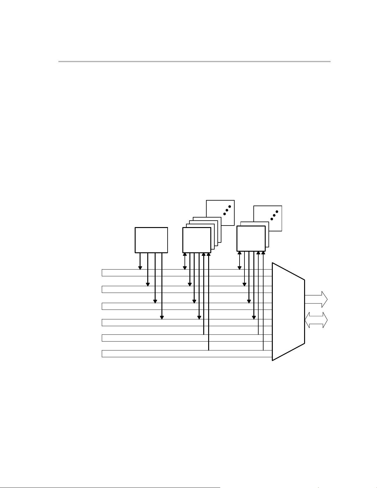
64 Conceptual Block Diagram of the DMA Controller Connections 123. . . . . . . . . . . . . . . . . . . . . .
65 High-Level Data Memory Map for DSP Subsystem 124. . . . . . . . . . . . . . . . . . . . . . . . . . . . . . . .
66 High-Level I/O Memory Map for DSP Subsystem 125. . . . . . . . . . . . . . . . . . . . . . . . . . . . . . . . . .
67 The Two Parts of a DMA Controller Transfer 125. . . . . . . . . . . . . . . . . . . . . . . . . . . . . . . . . . . . . .
68 Registers for Controlling the Context of a Channel 126. . . . . . . . . . . . . . . . . . . . . . . . . . . . . . . . .
69 DMA Channel Control Register (DMACCR) 127. . . . . . . . . . . . . . . . . . . . . . . . . . . . . . . . . . . . . . .
70 Auto-Initialization Sequence With Unchanging Context (REPEAT = 1) 130. . . . . . . . . . . . . . . .
71 Auto-initialization Sequence With Changing Context (REPEAT = 0) 131. . . . . . . . . . . . . . . . . .
72 MPUI Access Configurations 132. . . . . . . . . . . . . . . . . . . . . . . . . . . . . . . . . . . . . . . . . . . . . . . . . . .
73 One Possible Configuration for the Service Chains 133. . . . . . . . . . . . . . . . . . . . . . . . . . . . . . . .
74 Service Chain Applied to Three DMA Ports 136. . . . . . . . . . . . . . . . . . . . . . . . . . . . . . . . . . . . . . .
75 DSP GDMA Handler 147. . . . . . . . . . . . . . . . . . . . . . . . . . . . . . . . . . . . . . . . . . . . . . . . . . . . . . . . . . .
76 Functional Multiplexing DSP DMA Register A (FUNC_MUX_DSP_DMA_A) 150. . . . . . . . . . .
77 Functional Multiplexing DSP DMA Register B (FUNC_MUX_DSP_DMA_B) 151. . . . . . . . . . .
78 Functional Multiplexing DSP DMA Register C (FUNC_MUX_DSP_DMA_C) 153. . . . . . . . . .
79 Functional Multiplexing DSP DMA Register D (FUNC_MUX_DSP_DMA_D) 154. . . . . . . . . .
80 Triggering a Channel Interrupt Request 156. . . . . . . . . . . . . . . . . . . . . . . . . . . . . . . . . . . . . . . . . .
12 DSP Subsystem SPRU890A
Page 13

Figures
81 DMA Global Control Register (DMAGCR) 161. . . . . . . . . . . . . . . . . . . . . . . . . . . . . . . . . . . . . . . .
82 DMA Global Software Compatibility Register (DMAGSCR) 162. . . . . . . . . . . . . . . . . . . . . . . . .
83 DMA Global Timeout Control Register (DMAGTCR) 163. . . . . . . . . . . . . . . . . . . . . . . . . . . . . . .
84 DMA Channel Control Register (DMACCR) 165. . . . . . . . . . . . . . . . . . . . . . . . . . . . . . . . . . . . . . .
85 DMA Interrupt Control Register (DMACICR) and Status Register (DMACSR) 171. . . . . . . . .
86 DMA Source and Destination Parameters Register (DMACSDP) 175. . . . . . . . . . . . . . . . . . . .
87 DMA Source Start Address Registers (DMACSSAU and DMACSSAL) 179. . . . . . . . . . . . . . .
88 DMA Destination Start Address Registers (DMACDSAU and DMACDSAL) 181. . . . . . . . . . .
89 DMA Element Number Register (DMACEN) and Frame Number
Register (DMACFN) 182. . . . . . . . . . . . . . . . . . . . . . . . . . . . . . . . . . . . . . . . . . . . . . . . . . . . . . . . . . .
90 DMA Source Element Index Registers (DMACSEI, DMACDEI) and Frame
Index Registers (DMACSFI, DMACDFI) 185. . . . . . . . . . . . . . . . . . . . . . . . . . . . . . . . . . . . . . . . . .
91 DMA Source Address Counter (DMACSAC) and Destination Address
Counter (DMACDAC) 186. . . . . . . . . . . . . . . . . . . . . . . . . . . . . . . . . . . . . . . . . . . . . . . . . . . . . . . . . .
92 TIPB Control Mode Register (CMR) 192. . . . . . . . . . . . . . . . . . . . . . . . . . . . . . . . . . . . . . . . . . . . .
93 MPUI Mode Change Bits in ST3_55 196. . . . . . . . . . . . . . . . . . . . . . . . . . . . . . . . . . . . . . . . . . . . .
94 DSP MMU Endianess Control Register (DSP_ENDIAN_CONV) 201. . . . . . . . . . . . . . . . . . . . .
95 MPUI Control Register (CTRL_REG) 203. . . . . . . . . . . . . . . . . . . . . . . . . . . . . . . . . . . . . . . . . . . .
96 OMAP5910 DSP Subsystem Interrupts 205. . . . . . . . . . . . . . . . . . . . . . . . . . . . . . . . . . . . . . . . . .
97 OMAP5912 DSP Subsystem Interrupts 206. . . . . . . . . . . . . . . . . . . . . . . . . . . . . . . . . . . . . . . . . .
98 IFR0 and IER0 Bit Locations (OMAP5910) 209. . . . . . . . . . . . . . . . . . . . . . . . . . . . . . . . . . . . . . .
99 IFR1 and IER1 Bit Locations (OMAP5910) 210. . . . . . . . . . . . . . . . . . . . . . . . . . . . . . . . . . . . . . .
100 IFR0 and IER0 Bit Locations (OMAP5912) 212. . . . . . . . . . . . . . . . . . . . . . . . . . . . . . . . . . . . . . .
101 IFR1 and IER1 Bit Locations (OMAP5912) 212. . . . . . . . . . . . . . . . . . . . . . . . . . . . . . . . . . . . . . .
102 OMAP Clock Generation 217. . . . . . . . . . . . . . . . . . . . . . . . . . . . . . . . . . . . . . . . . . . . . . . . . . . . . . .
103 DSP Clock Domain 217. . . . . . . . . . . . . . . . . . . . . . . . . . . . . . . . . . . . . . . . . . . . . . . . . . . . . . . . . . . .
104 Generation of DSP Subsystem Master Clock and DSP MMU Clock 218. . . . . . . . . . . . . . . . . .
105 Idle Configuration Process 221. . . . . . . . . . . . . . . . . . . . . . . . . . . . . . . . . . . . . . . . . . . . . . . . . . . . .
106 Idle Control Register (ICR) 225. . . . . . . . . . . . . . . . . . . . . . . . . . . . . . . . . . . . . . . . . . . . . . . . . . . . .
107 Idle Status Register (ISTR) 226. . . . . . . . . . . . . . . . . . . . . . . . . . . . . . . . . . . . . . . . . . . . . . . . . . . . .
108 DSP Boot Configuration Register (DSP_BOOT_CONFIG) 230. . . . . . . . . . . . . . . . . . . . . . . . . .
13DSP SubsystemSPRU890A
Page 14

Tables
Tables
1 OMAP5910/5912 DSP Subsystem Global Memory Map 29. . . . . . . . . . . . . . . . . . . . . . . . . . . . .
2 Fetch Address Field Descriptions for the 2-Way Cache Register Field Descriptions 36. . . . .
3 Fetch Address Field Descriptions for a RAM Set 36. . . . . . . . . . . . . . . . . . . . . . . . . . . . . . . . . . .
4 Instruction Presence Check and I-Cache Response 37. . . . . . . . . . . . . . . . . . . . . . . . . . . . . . . .
5 Summary of the I-Cache Registers 48. . . . . . . . . . . . . . . . . . . . . . . . . . . . . . . . . . . . . . . . . . . . . . .
6 I-Cache Global Control Register (GCR) Bits Field Descriptions 50. . . . . . . . . . . . . . . . . . . . . . .
7 I-Cache Line Flush Register 0 (FLR0) Field Descriptions 52. . . . . . . . . . . . . . . . . . . . . . . . . . . .
8 I-Cache Line Flush Register 1 (FLR1) Field Descriptions 52. . . . . . . . . . . . . . . . . . . . . . . . . . . .
9 I-Cache N-way Control Register (NWCR) Field Descriptions 53. . . . . . . . . . . . . . . . . . . . . . . . .
10 I-Cache RAM Set 1 Control Register (RCR1) and RAM Set 2 Control Register
11 I-Cache RAM Set 1 Tag Register (RTR1) Field Descriptions 56. . . . . . . . . . . . . . . . . . . . . . . . .
12 I-Cache RAM Set 2 Tag Register (RTR2) Field Descriptions 56. . . . . . . . . . . . . . . . . . . . . . . . .
13 I-Cache Status Register (ISR) Field Descriptions 57. . . . . . . . . . . . . . . . . . . . . . . . . . . . . . . . . . .
14 EMIF Requests and Their Priorities 60. . . . . . . . . . . . . . . . . . . . . . . . . . . . . . . . . . . . . . . . . . . . . . .
15 EMIF Requests Associated with Dual and Long Data Accesses 61. . . . . . . . . . . . . . . . . . . . . .
16 Summary of the EMIF Registers 63. . . . . . . . . . . . . . . . . . . . . . . . . . . . . . . . . . . . . . . . . . . . . . . . .
17 EMIF Global Control Register (GCR) Field Descriptions 64. . . . . . . . . . . . . . . . . . . . . . . . . . . . .
18 EMIF Global Reset Register (GRR) Field Descriptions 64. . . . . . . . . . . . . . . . . . . . . . . . . . . . . .
19 First−Level Descriptor Contents 86. . . . . . . . . . . . . . . . . . . . . . . . . . . . . . . . . . . . . . . . . . . . . . . . . .
20 First−Level Descriptor Contents 89. . . . . . . . . . . . . . . . . . . . . . . . . . . . . . . . . . . . . . . . . . . . . . . . . .
21 Summary of DSP MMU Registers 101. . . . . . . . . . . . . . . . . . . . . . . . . . . . . . . . . . . . . . . . . . . . . . .
22 MMU Pre-Fetch Register (PREFETCH_REG) Field Descriptions 103. . . . . . . . . . . . . . . . . . . .
23 MMU Pre-Fetch Status Register (WALKING_ST_REG) Field Descriptions 104. . . . . . . . . . . .
24 Control Register (CNTL_REG) Field Descriptions 105. . . . . . . . . . . . . . . . . . . . . . . . . . . . . . . . .
25 MMU MSB Fault Address Register (FAULT_AD_H_REG) Field Descriptions 106. . . . . . . . . .
26 MMU LSB Fault Address Register (FAULT_AD_L_REG) Field Descriptions 106. . . . . . . . . . .
27 MMU Fault Status Register (FAULT_ST_REG) Field Descriptions 107. . . . . . . . . . . . . . . . . . .
28 MMU Interrupt Acknowledge Register (IT_ACK_REG) Field Descriptions 109. . . . . . . . . . . . .
29 MMU MSB Translation Table Register (TTB_H_REG) Field Descriptions 110. . . . . . . . . . . . .
30 MMU LSB Translation Table Register (TTB_L_REG) Field Descriptions 110. . . . . . . . . . . . . .
31 MMU Lock/Protect Entry Register (LOCK_REG) Field Descriptions 111. . . . . . . . . . . . . . . . . .
32 MMU Read/Write TLB Entry Register (LD_TLB_REG) Field Descriptions 112. . . . . . . . . . . . .
33 MMU MSB CAM Entry Register (CAM_H_REG) Field Descriptions 113. . . . . . . . . . . . . . . . . .
34 MMU LSB CAM Entry Register (CAM_L_REG) Field Descriptions 113. . . . . . . . . . . . . . . . . . .
35 MMU MSB RAM Entry Register (RAM_H_REG) Field Descriptions 114. . . . . . . . . . . . . . . . . .
(RCR2) Field Descriptions 55. . . . . . . . . . . . . . . . . . . . . . . . . . . . . . . . . . . . . . . . . . . . . . . . . . . . . . .
14 DSP Subsystem SPRU890A
Page 15

Tables
36 MMU LSB RAM Entry Register (RAM_L_REG) Field Descriptions 114. . . . . . . . . . . . . . . . . . .
37 MMU TLB Global Flush Register (GFLUSH_REG) Field Descriptions 115. . . . . . . . . . . . . . . .
38 MMU TLB Entry Flush Register (FLUSH_ENTRY_REG) Field Descriptions 116. . . . . . . . . . .
39 MMU MSB CAM Entry Read Register (READ_CAM_H_REG) Field Descriptions 117. . . . . .
40 MMU LSB CAM Entry Read Register (READ_CAM_L_REG) Field Descriptions 118. . . . . . .
41 MMU MSB RAM Entry Read Register (READ_RAM_H_REG) Field Descriptions 119. . . . . .
42 MMU LSB RAM Entry Read Register (READ_RAM_L_REG) Field Descriptions 120. . . . . . .
43 MMU Idle Control Register (DSPMMU_IDLE_CTRL) Field Descriptions 120. . . . . . . . . . . . . .
44 DMA Channel Control Register (DMACCR) Field Descriptions 128. . . . . . . . . . . . . . . . . . . . . .
45 Activity Shown in 74 135. . . . . . . . . . . . . . . . . . . . . . . . . . . . . . . . . . . . . . . . . . . . . . . . . . . . . . . . . . .
46 Registers Used to Define the Start Addresses for a DMA Transfer 137. . . . . . . . . . . . . . . . . . .
47 DMA Controller Ports 139. . . . . . . . . . . . . . . . . . . . . . . . . . . . . . . . . . . . . . . . . . . . . . . . . . . . . . . . . .
48 DMA Controller Data Packing 140. . . . . . . . . . . . . . . . . . . . . . . . . . . . . . . . . . . . . . . . . . . . . . . . . . .
49 Read/Write Synchronization 143. . . . . . . . . . . . . . . . . . . . . . . . . . . . . . . . . . . . . . . . . . . . . . . . . . . .
50 DSP DMA Controller Synchronization Events for OMAP5910 145. . . . . . . . . . . . . . . . . . . . . . .
51 DSP DMA Controller Synchronization Events for OMAP5912 146. . . . . . . . . . . . . . . . . . . . . . .
52 DSP GDMA Handler Input Request Lines 147. . . . . . . . . . . . . . . . . . . . . . . . . . . . . . . . . . . . . . . .
53 Registers of the OMAP5912 DSP GDMA Handler 149. . . . . . . . . . . . . . . . . . . . . . . . . . . . . . . . .
54 Functional Multiplexing DSP DMA Register A (FUNC_MUX_DSP_DMA_A)
Field Descriptions 150. . . . . . . . . . . . . . . . . . . . . . . . . . . . . . . . . . . . . . . . . . . . . . . . . . . . . . . . . . . . .
55 Functional Multiplexing DSP DMA Register B (FUNC_MUX_DSP_DMA_B)
Field Descriptions 152. . . . . . . . . . . . . . . . . . . . . . . . . . . . . . . . . . . . . . . . . . . . . . . . . . . . . . . . . . . . .
56 Functional Multiplexing DSP DMA Register C (FUNC_MUX_DSP_DMA_C)
Field Descriptions 153. . . . . . . . . . . . . . . . . . . . . . . . . . . . . . . . . . . . . . . . . . . . . . . . . . . . . . . . . . . . .
57 Functional Multiplexing DSP DMA Register D (FUNC_MUX_DSP_DMA_D)
Field Descriptions 154. . . . . . . . . . . . . . . . . . . . . . . . . . . . . . . . . . . . . . . . . . . . . . . . . . . . . . . . . . . . .
58 DMA Controller Operational Events and Their Associated Bits and Interrupts 155. . . . . . . . .
59 Registers of the DMA Controller 160. . . . . . . . . . . . . . . . . . . . . . . . . . . . . . . . . . . . . . . . . . . . . . . . .
60 DMA Global Control Register (DMAGCR) Field Descriptions 161. . . . . . . . . . . . . . . . . . . . . . . .
61 DMA Global Software Compatibility Register (DMAGSCR) Field Descriptions 163. . . . . . . . .
62 DMA Global Timeout Control Register (DMAGTCR) Field Descriptions 164. . . . . . . . . . . . . . .
63 DMA Channel Control Register (DMACCR) Field Descriptions 165. . . . . . . . . . . . . . . . . . . . . .
64 DMA Interrupt Control Register (DMACICR) Fields Descriptions 171. . . . . . . . . . . . . . . . . . . . .
65 DMA Status Register (DMACSR) Field Descriptions 173. . . . . . . . . . . . . . . . . . . . . . . . . . . . . . .
66 DMA Source and Destination Parameters Register (DMACSDP) Field Descriptions 175. . . .
67 DMA Source Start Address Register − Upper Part (DMACSSAU) Field Descriptions 180. . .
68 DMA Source Start Address Register − Lower Part (DMACSSAL) Field Descriptions 180. . .
69 DMA Destination Start Address Register − Upper Part (DMACDSAU)
Field Descriptions 181. . . . . . . . . . . . . . . . . . . . . . . . . . . . . . . . . . . . . . . . . . . . . . . . . . . . . . . . . . . . .
70 DMA Destination Start Address Register − Lower Part (DMACDSAL)
Field Descriptions 181. . . . . . . . . . . . . . . . . . . . . . . . . . . . . . . . . . . . . . . . . . . . . . . . . . . . . . . . . . . . .
71 DMA Element Number Register (DMACEN) Field Descriptions 182. . . . . . . . . . . . . . . . . . . . . .
72 Frame Number Register (DMACFN) Field Descriptions 182. . . . . . . . . . . . . . . . . . . . . . . . . . . .
73 DMA Source Element Index Register (DMACSEI/DMACEI) Field Descriptions 185. . . . . . . .
74 DMA Source Frame Index Register (DMACSFI / DMACFI) Field Descriptions 185. . . . . . . . .
15DSP SubsystemSPRU890A
Page 16

Tables
75 DMA Destination Element Index Register (DMACDEI) Field Descriptions 186. . . . . . . . . . . . .
76 DMA Destination Frame Index Register (DMACDFI) Field Descriptions 186. . . . . . . . . . . . . .
77 DMA Source Address Counter (DMACSAC) Field Descriptions 186. . . . . . . . . . . . . . . . . . . . . .
78 DMA Destination Address Counter (DMACDAC) Field Descriptions 186. . . . . . . . . . . . . . . . . .
79 TIPB Access Rates 189. . . . . . . . . . . . . . . . . . . . . . . . . . . . . . . . . . . . . . . . . . . . . . . . . . . . . . . . . . . .
80 Peripherals Affected by Access Factor Bits (OMAP5912) 190. . . . . . . . . . . . . . . . . . . . . . . . . . .
81 Peripherals Affected by Access Factor Bits (OMAP5910) 190. . . . . . . . . . . . . . . . . . . . . . . . . . .
82 Register of the TIPB Bridge 191. . . . . . . . . . . . . . . . . . . . . . . . . . . . . . . . . . . . . . . . . . . . . . . . . . . .
83 TIPB Control Mode Register (CMR) Field Descriptions 192. . . . . . . . . . . . . . . . . . . . . . . . . . . . .
84 HOM_R and HOM_P Bits in DSP Core Register ST3_55 197. . . . . . . . . . . . . . . . . . . . . . . . . . .
85 Little-Endian versus Big-Endian Data Format 197. . . . . . . . . . . . . . . . . . . . . . . . . . . . . . . . . . . . .
86 Big-Endian Access of Little-Endian Data 199. . . . . . . . . . . . . . . . . . . . . . . . . . . . . . . . . . . . . . . . .
87 Effect of DSP MMU Endianess Conversion Settings 200. . . . . . . . . . . . . . . . . . . . . . . . . . . . . . .
88 DSP MMU Endianess Control Register (DSP_ENDIAN_CONV) Field Descriptions 201. . . .
89 Effect of MPUI Endianess Conversion Settings 202. . . . . . . . . . . . . . . . . . . . . . . . . . . . . . . . . . . .
90 MPUI Control Register (CTRL_REG) Field Descriptions 203. . . . . . . . . . . . . . . . . . . . . . . . . . . .
91 OMAP5910 Level 1 Interrupt Mapping 208. . . . . . . . . . . . . . . . . . . . . . . . . . . . . . . . . . . . . . . . . . .
92 OMAP5912 Level 1 Interrupt Mapping 210. . . . . . . . . . . . . . . . . . . . . . . . . . . . . . . . . . . . . . . . . . .
93 OMAP5910 Level 2 Interrupt Mapping 213. . . . . . . . . . . . . . . . . . . . . . . . . . . . . . . . . . . . . . . . . . .
94 OMAP5912 Level 2.0 Interrupt Mapping 214. . . . . . . . . . . . . . . . . . . . . . . . . . . . . . . . . . . . . . . . . .
95 OMAP5912 Level 2.1 Interrupt Mapping 214. . . . . . . . . . . . . . . . . . . . . . . . . . . . . . . . . . . . . . . . . .
96 Idle Domains in the DSP 219. . . . . . . . . . . . . . . . . . . . . . . . . . . . . . . . . . . . . . . . . . . . . . . . . . . . . . .
97 Changing Idle Configurations 222. . . . . . . . . . . . . . . . . . . . . . . . . . . . . . . . . . . . . . . . . . . . . . . . . . .
98 DSP Core Response After Reactivation 223. . . . . . . . . . . . . . . . . . . . . . . . . . . . . . . . . . . . . . . . . .
99 Registers for DSP Module Idle Control 225. . . . . . . . . . . . . . . . . . . . . . . . . . . . . . . . . . . . . . . . . . .
100 Idle Control Register (ICR) Field Descriptions 226. . . . . . . . . . . . . . . . . . . . . . . . . . . . . . . . . . . . .
101 Idle Status Register (ISTR) Field Descriptions 227. . . . . . . . . . . . . . . . . . . . . . . . . . . . . . . . . . . .
102 DSP PDROM Contents 229. . . . . . . . . . . . . . . . . . . . . . . . . . . . . . . . . . . . . . . . . . . . . . . . . . . . . . . .
103 Bootloader Initialization 229. . . . . . . . . . . . . . . . . . . . . . . . . . . . . . . . . . . . . . . . . . . . . . . . . . . . . . . .
104 DSP Boot Configuration Register (DSP_BOOT_CONFIG) Field Descriptions 230. . . . . . . . .
105 Registers for DSP Module Idle Control 231. . . . . . . . . . . . . . . . . . . . . . . . . . . . . . . . . . . . . . . . . . .
106 Document Revision History 234. . . . . . . . . . . . . . . . . . . . . . . . . . . . . . . . . . . . . . . . . . . . . . . . . . . . .
16 DSP Subsystem SPRU890A
Page 17

1 Digital Signal Processor Subsystem Overview
1.1 Architecture Overview
The Digital Signal Processor (DSP) Subsystem is a collection of modules
which include the TMS320C55x CPU processor along with its hardware
accelerators, tightly coupled memory, instruction cache, and dedicated DMA,
the interfaces it uses to communicate with rest of the OMAP device, as well
as a number of peripherals.
The TMS320C55x core processor (also referred to as the DSP core) and the
peripherals included in the DSP subsystem communicate with:
- The MPU core via the microprocessor unit interface (MPUI)
- Various standard memories via the external memory interface (EMIF)
- Various system peripherals via two TI peripheral bus (TIPB) bridges
Figure 1 and Figure 2 in section 1.4 show block diagrams for the OMAP5910
and OMAP5912 DSP subsystems.
DSP Subsystem
1.2 Features
The DSP subsystem is composed of several portions: the DSP module, the
peripherals that surround that module, and several interfaces used to
communicate with the rest of the OMAP modules. Each portion has the
following components:
- DSP module:
J TMS320C55x (C55x) DSP core
J Tightly coupled hardware accelerators: discrete cosine
transform/inverse discrete cosine transform (DCT/IDCT), motion
estimation, and half-pixel interpolation
J Tightly coupled memories and their interfaces: dual-access RAM
(DARAM), single-access RAM (SARAM), programmable dynamic
ROM, and an instruction cache (I-Cache)
J Six-channel DMA controller that can copy memory contents from one
address to another without DSP core intervention
17DSP SubsystemSPRU890A
Page 18

Digital Signal Processor Subsystem Overview
DSP subsystem interfaces:
-
J External memory interface (EMIF) that connects the DSP core to
external and loosely coupled memories
J MPUI port that permits access to DSP resources by the MPU and
system DMA
J TIPB that provides two external bus interfaces for private and public
peripherals
- DSP subsystem peripherals:
J Private peripherals are on the DSP private peripheral bus, and can
only be accessed by the DSP core. DSP private peripherals include:
H Three 32-bit timers
H Watchdog timer
H Interrupt handlers
J Public peripherals are on the DSP public peripheral bus. These
peripherals are directly accessible by the DSP core and DSP DMA.
The MPU core can also access these peripherals through the MPUI
port. DSP public peripherals include:
H Two multichannel buffered serial ports (McBSPs)
H Two multichannel serial interfaces (MCSIs)
J The DSP core and DMA controller also have access to system
peripherals (also referred to as shared peripherals). Shared
peripherals are connected to both the MPU public peripheral bus and
the DSP public peripheral bus. Shared peripherals include:
H Mailbox module to permit interrupt-based signaling between the
DSP and MPU cores
H Three universal asynchronous receiver/transmitter (UART)
modules
H General-purpose input/output (GPIO) module
J The OMAP5912 also adds these shared peripherals:
H Eight general purpose timers
H Serial port interface (SPI)
H I2C master/slave interface
H Extra McBSP
H Multimedia card/secure digital interface (MMC/SDIO)
H 32-KHz synchronization counter
This document describes all of the DSP module components listed above. The
DSP subsystem peripherals are described in separate documents.
DSP Subsystem18 SPRU890A
Page 19
Digital Signal Processor Subsystem Overview
1.3 Differences Between the OMAP5910 and OMAP5912 DSP
Subsystems
The OMAP5910 and OMAP5912 DSP subsystems are very similar. The
difference between the subsystems lies in the mix of the MPU/DSP shared
peripherals.
1.4 Functional Block Diagrams
Figure 1 and Figure 2 show functional block diagrams of the OMAP5910 and
OMAP5912 DSP subsystems.
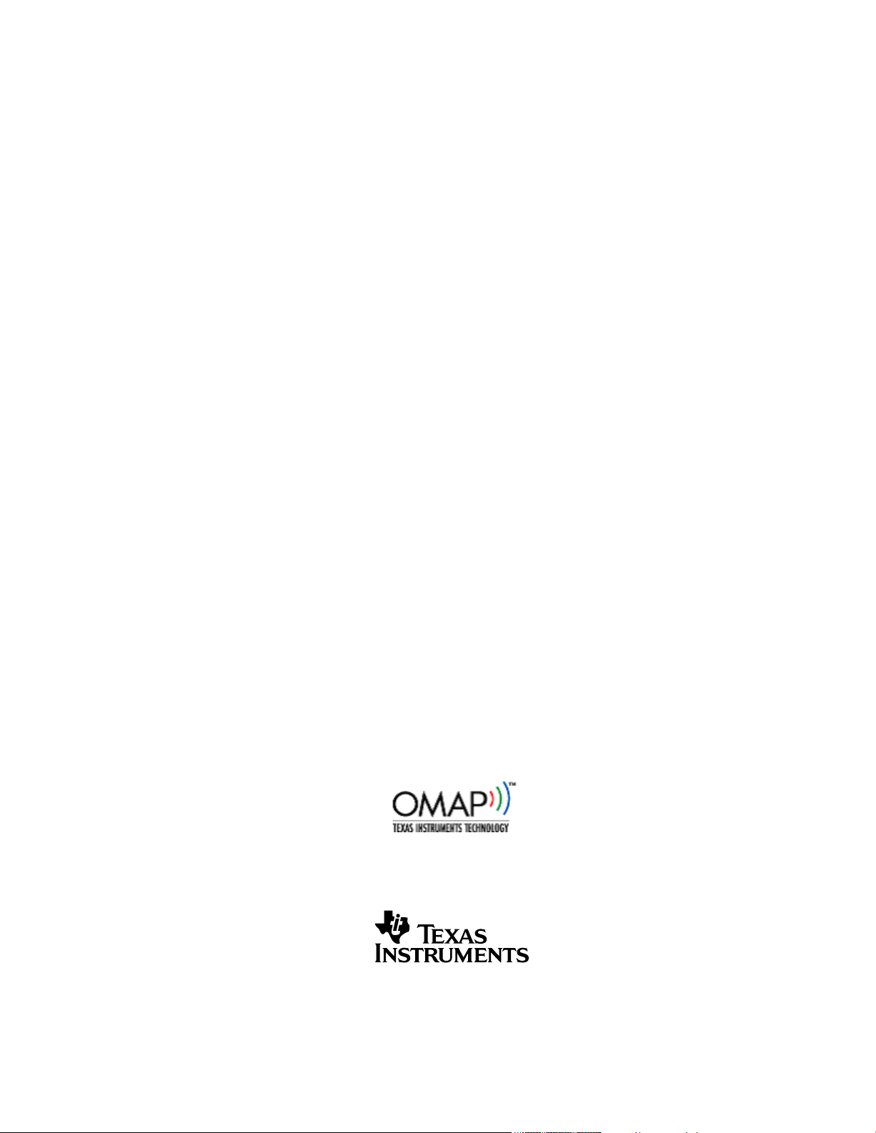
Figure 1. OMAP5910 DSP Subsystem and Modules
DSP Subsystem and Interfaces
DSP private
peripherals
Timers
Watchdog
timer
Interrupt
handlers
Interrupt
interface
DSP private
peripheral bus
DSP public
peripheral bus
DSP public
peripherals
ROM,
SRAM,
Flash,
SBFlash
SDRAM
Endianess
conversion
DSP
MMU
controller
On-chip
SRAM
Traffic
EMIF
I-Cache
DARAM
SARAM
DSP Module
Internal
memory
buses
Memory
I/F
Configuration
DMA
(EMIF)
(DARAM)
(SARAM)
(MPUI)
(TIPB)
MPUI port
HWA
TMS320C55x
DSP core
Shared
TIPB
bridge
Private
TIPB
bridge
Pseudo
dynamic
sharing
MPU/DSP shared
peripherals
Mailbox
GPIO I/F
UART1,2,3
Static UART
sharing switch
16
16
Endianess conversion
MPU
subsystem
System
DMA
MPUI
MPU
MPU public
peripheral
bus
MPU public
TIPB bridge
McBSP1
McBSP3
MCSI2
MCSI1
19DSP SubsystemSPRU890A
Page 20
Digital Signal Processor Subsystem Overview
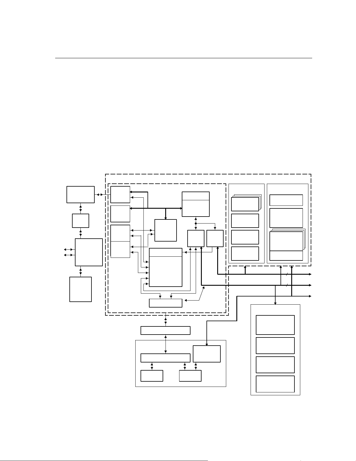
Figure 2. OMAP5912 DSP Subsystem and Modules
DSP Subsystem and Interfaces
DSP Module
Internal
memory
buses
Memory
I/F
Configuration
DMA
(EMIF)
(DARAM)
(SARAM)
(MPUI)
(TIPB)
MPUI port
HWA
TMS320C55x
DSP core
Shared
TIPB
bridge
Pseudo
dynamic
sharing
ROM,
SRAM,
Flash,
SBFlash
SDRAM
Endianess
conversion
DSP
MMU
Traffic
controller
On-chip
SRAM
EMIF
I-Cache
DARAM
SARAM
Private
TIPB
bridge
DSP private
peripherals
Timers
Watchdog
timer
Interrupt
handlers
Interrupt
interface
DSP private
peripheral bus
DSP public
peripheral bus
MPU/DSP shared
peripherals
Mailbox
MPU/DSP static
shared
8xGPTIMERS
SPI
UART1,2,3
I2C
MMCSDIO2
McBSP2
MPU/DSP
Dynamic shared
GPIO1,2,3,4
32-KHz synchro timer
16
16
DSP public
peripherals
Endianess conversion
MPU
subsystem
System
DMA
MPUI
MPU
MPU public
peripheral
bus
MPU public
TIPB bridge
McBSP1
McBSP3
MCSI2
MCSI1
DSP Subsystem20 SPRU890A
Page 21

2 C55x DSP Core Overview
The DSP subsystem is based on the TMS320C55x DSP generation processor
core. This section is intended to give a mere overview of the C55x DSP core.
For detailed information, see the TMS320C55x DSP CPU Reference Guide
(SPRU371).
2.1 DSP Core Features
Features of the high-performance, low-power DSP core include:
- Advanced multiple-bus architecture with one internal program memory
bus and five internal data buses (three dedicated to reads and two
dedicated to writes)
- Unified program/data memory architecture
- Dual 17-bit x 17-bit multipliers coupled to 40-bit dedicated adders for
non-pipelined single-cycle multiply accumulate (MAC) operations
- Two address generators with eight auxiliary registers and two auxiliary
register arithmetic units
C55x DSP Core Overview
- 8M x 16 bits (16M bytes) of total addressable memory space
- Single-instruction repeat or block repeat operations for program code
- Conditional execution
- Seven-stage pipeline for high instruction throughput
- Instruction buffer unit that loads, parses, queues, and decodes
instructions to decouple the program fetch function from the pipeline
- Program flow unit that coordinates program actions among multiple
parallel DSP core functional units
- Address data flow unit that provides data address generation and includes
a 16-bit arithmetic unit capable of performing arithmetical, logical, shift,
and saturation operations
- Data computation unit containing the primary computation units of the
DSP core, including a 40-bit arithmetic logic unit, two MAC units, and a
shifter
- Software-programmable idle domains that provide configurable
low-power modes
- Automatic power management
21DSP SubsystemSPRU890A
Page 22

C55x DSP Core Overview
2.2 Introduction to the DSP Core
The DSP core supports an internal bus structure composed of one program
bus, three data read buses, two data write buses, and additional buses
dedicated to peripheral and DMA controller activity. These buses provide the
ability to perform up to three data reads and two data writes in a single cycle.
The DSP core provides two multiply-accumulate (MAC) units, each capable
of 17-bit x 17-bit multiplication in a single cycle. A central 40-bit arithmetic/logic
unit (ALU) is supported by an additional 16-bit ALU. Use of the ALUs is under
instruction set control, providing the ability to optimize parallel activity and
power consumption. These resources are managed in the address unit (AU)
and data unit (DU) of the DSP core.
The DSP core supports a variable byte width instruction set for improved code
density. The instruction unit (IU) performs 32-bit program fetches from internal
or DSP external memory and queues instructions for the program unit (PU).
The program unit decodes the instructions, directs tasks to AU and DU
resources, and manages the fully protected pipeline. Predictive branching
capability avoids pipeline flushes on execution of conditional instructions.
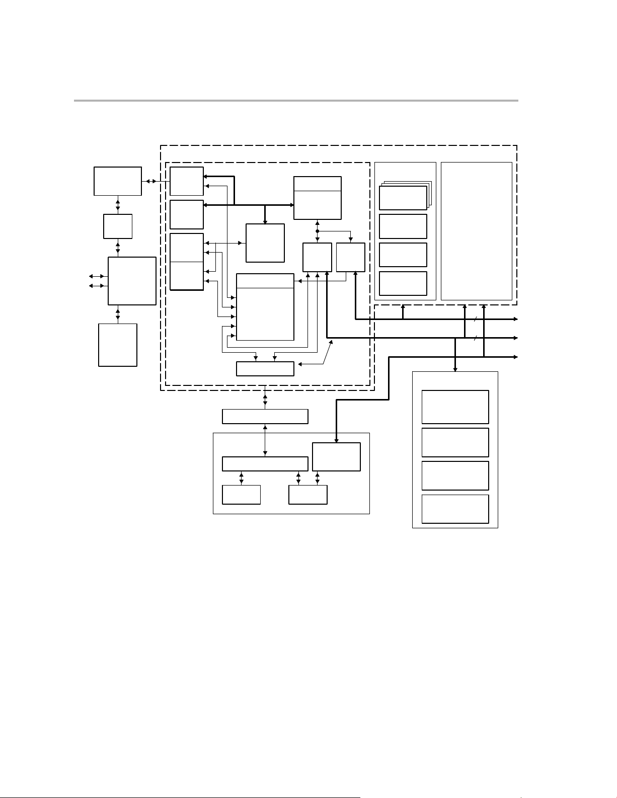
Figure 3 shows a conceptual block diagram of the DSP core. Detailed
information on each of the buses and units represented in this figure are given
in the TMS320C55x DSP CPU Reference Guide (SPRU371).
DSP Subsystem22 SPRU890A
Page 23
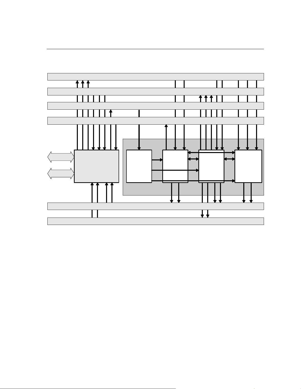
Figure 3. DSP Core Diagram
C55x DSP Core Overview
Data-read data buses BB, CB, DB (each 16 bits)
Data-read address buses BAB, CAB, DAB (each 23 bits)
Program-read data bus PB (32 bits)
Program-read address bus PAB (24 bits)
External data
buses
External
program buses
Memory
interface unit
Other useful documents include:
- TMS320C55x DSP Mnemonic Instruction Set Reference Guide
- TMS320C55x Programmer’s Guide (SPRU376): Describes ways to
CPU
Instruction
buffer unit
(I unit)
Data-write data buses EB, FB (each 16 bits)
Data-write address buses EAB, FAB (each 23 bits)
Program
flow unit
(P unit)
Address-data
flow unit
(A unit)
Data
computation
unit
(D unit)
(SPRU374): Describes the mnemonic instructions individually. It also
includes a summary of the instruction set, a list of the instruction opcodes,
and a cross-reference to the algebraic instruction set.
optimize C and assembly code for the TMS320C55x DSPs and explains
how to write code that uses the special features and instructions of the
DSP.
- TMS320C55x Optimizing C Compiler User’s Guide (SPRU281):
Describes the TMS320C55x C Compiler. This C compiler accepts ANSI
standard C source code and produces assembly language source code
for TMS320C55x devices.
23DSP SubsystemSPRU890A
Page 24

C55x DSP Core Overview
TMS320C55x Assembly Language Tools User’s Guide (SPRU280):
-
Describes the assembly language tools (assembler, linker, and other tools
used to develop assembly language code), assembler directives, macros,
common object file format, and symbolic debugging directives for
TMS320C55x devices.
2.3 Introduction to the Hardware Accelerators
Three powerful C55x hardware accelerator modules assist the DSP core in
implementing algorithms that are commonly used in video compression
applications such as MPEG4 encoders/decoders. These accelerators allow
implementation of such algorithms using fewer DSP instruction cycles and
dissipating less power than if the DSP core were operating alone. The
hardware accelerators are utilized via functions from the TMS320C55x
Image/Video Processing Library available from Texas Instruments.
The Image/Video Processing Library implements many useful functions
utilizing the hardware accelerators, including:
- Forward and Inverse Discrete Cosine Transform (DCT) (used for video
compression/decompression)
- Motion Estimation (used for compression standards such as MPEG video
encoding and H.26x encoding)
- Pixel Interpolation (enabling high-performance fractal pixel motion
estimation)
- Quantization/Dequantization (useful for JPEG, MPEG, H.26x
encoding/decoding)
- Flexible 1D/2D Wavelet Processing (useful for JPEG2000, MPEG4, and
other compression standards)
- Boundary and Perimeter Computation (useful for Machine Vision
applications)
- Image Threshold and Histogram Computations (useful for various Image
Analysis applications)
More information on the C55x Image/Video Processing Library can be found
in the TMS320C55x Image/Video Processing Library Programmer’s
Reference (SPRU037).
DSP Subsystem24 SPRU890A
Page 25

C55x DSP Core Overview
There are three hardware accelerators included along with the C55x DSP
core:
- DCT/IDCT Accelerator: This hardware accelerator implements Forward
and Inverse DCT algorithms. These DCT/IDCT algorithms can enable a
wide range of video compression standards including JPEG
Encode/Decode, MPEG Video Encode/Decode, and H.26x
Encode/Decode.
- Motion Estimation Accelerator: This hardware accelerator implements a
high-performance motion estimation algorithm, enabling MPEG Video
encoder or H.26x encoder applications. Motion estimation is typically one
of the most computation-intensive operations in video-encoding systems.
- Pixel Interpolation Accelerator: This hardware accelerator enables
high-performance pixel-interpolation algorithms, which allow for powerful
fractal pixel motion estimation when used in conjunction with the Motion
Estimation Accelerator. Such algorithms provide significant improvement
to video-encoding applications.
Detailed information on the C55x Hardware Accelerators can be found in the
TMS320C55x Hardware Extensions for Image/Video Applications
Programmer’s Reference (SPRU098).
25DSP SubsystemSPRU890A
Page 26

DSP Subsystem Memory
3 DSP Subsystem Memory
The DSP subsystem requires access to three different types of memory:
program memory, data memory, and I/O memory. The DSP subsystem
architecture uses a unified program and data memory space composed of
memory internal and external to the DSP subsystem. Internal memory is made
up of tightly coupled memory blocks, whereas DSP external memory is
mapped to OMAP system memory. The DSP subsystem architecture provides
access to a maximum of 8M words (16M bytes) of program/data memory
space.
The DSP subsystem I/O memory space is separate from the data/program
memory space. The I/O space includes the configuration and data registers
for all peripherals accessible by the DSP subsystem.
3.1 Internal Memory Space
The DSP subsystem memory consists of four types of tightly coupled
memories which provide the DSP core with maximum efficiency.
- Dual-access RAM (DARAM)
The DARAM memory consists of 8 blocks of 8K bytes each. The DARAM
(64K bytes) can support up to two memory accesses into each RAM block
in one DSP core clock cycle. Accesses can be made from any internal
data, program, or DMA bus.
- Single-access RAM (SARAM)
The SARAM memory consists of 12 blocks of 8K bytes each. The SARAM
(96K bytes) can support one memory access into each RAM block in one
DSP core clock cycle. This access can be a 32-bit value. Accesses can be
made from any internal data, program, or DMA bus.
- Programmable dynamic ROM (PDROM)
The PDROM memory consists of 1 block of 32K bytes. The programmable
dynamic ROM (32K bytes) can support one memory read in one DSP core
clock cycle. This access can be a 32-bit value. Accesses can be made
from any internal data read or program bus.
The PDROM contains a program called a bootloader, which is executed by
the DSP core when it is taken out of reset. Depending on the boot mode
selected, the DSP core will either branch to an internal or DSP external
memory address, or go into idle. Note that the memory at the destination
address must be initialized with valid code before the bootloader is
executed. Selecting boot mode 000b will disable the PDROM. The MPU
core specifies the boot mode through the DSP_BOOT_CONFIG register.
For more information on the DSP subsystem bootloader and the
DSP_BOOT_CONFIG register, see section 12.4.
DSP Subsystem26 SPRU890A
Page 27
Configurable I-Cache structure
-
The DSP instruction cache (I-Cache) module is a special-purpose, tightly
coupled, RAM-based program memory. The module is designed to
significantly improve DSP core performance by buffering the instructions
most recently fetched from DSP external memory. The entire external
program memory space is cacheable. Section 4 describes the I-Cache in
more detail.
Figure 4 shows the connections between the internal memory blocks and the
buses of the DSP core.
Figure 4. Internal Memory Connections in the DSP Subsystem
12 blocks of 8K bytes
8 blocks of 8K bytes
1 block of 32K bytes
DSP Subsystem Memory
P buses
B buses
C buses
D buses
E buses
F bus
PDROM
SARAM
DARAM
To
external
memory
I/F
A
D
The DSP core uses the six sets of buses to simultaneously fetch up to 32 bits
of program code and to read up to 48 bits of data from memory (or to write up
to 32 bits of data to memory). To achieve maximum performance from the
architecture, pay close attention to placement of code and data structures
within the on-chip memory resources. For more details, see the TMS320C55x
Programmer’s Guide (SPRU376).
27DSP SubsystemSPRU890A
Page 28

DSP Subsystem Memory
3.2 DSP External Memory Space
The DSP core and DMA controller use the external memory interface (EMIF)
to access the DSP external memory. External memory for the DSP subsystem
ranges from byte address 0x02 8000 to 0xFF 8000 if the internal PDROM is
enabled, or to 0xFF FFFF if the PDROM is not enabled. See Figure 18 for more
details.
Note:
The term DSP external memory refers to memory outside of the DSP
subsystem internal memory space. This includes program addresses in the
range of 0x02 8000 to 0xFF 8000 if the internal PDROM is enabled, or to
0xFF FFFF if the PDROM is not enabled.
All DSP external memory access requests are passed through the DSP
memory management unit (MMU). If this unit is enabled and configured by the
MPU core, it translates the DSP external memory access request address,
also called a virtual address, into a system memory address, also called a
physical address, that is then passed to the traffic controller. The traffic
controller completes the memory access through one of the three system
memory interfaces: internal memory (IMIF), slow external memory (EMIFS),
or fast external memory (EMIFF).
If the MMU is not enabled, then the access request is passed directly to the
system traffic controller. In this case, the DSP virtual address is mapped to the
first 16M bytes of chip select space 0 (CS0) of the system memory.
3.3 I/O Memory Space
The DSP subsystem I/O space is a separate address space from the
data/program memory space. Configuration and data registers for all
peripherals reside in the DSP subsystem I/O space, which consists of
64K-word addresses. Each peripheral maps into a 1K-word section of I/O
memory.
OMAP devices include sets of peripherals grouped into three main categories:
shared, public, or private.
- DSP/MPU shared peripherals are connected to both the MPU public
peripheral bus and the DSP public peripheral bus. Connections are routed
through a TI peripheral bus switch, which must be configured to allow MPU
domain or DSP domain access. Some shared peripherals have
permanent connections to both public peripheral buses, although read
and write accesses to each peripheral register may differ.
DSP Subsystem28 SPRU890A
Page 29

DSP Subsystem Memory
DSP public peripherals are connected to the DSP public peripheral bus
-
and are directly accessible by the DSP core and DSP DMA. These
peripherals may also be accessed by the MPU core and system DMA
controller via the MPUI.
- DSP private peripherals are on the DSP private peripheral bus, and thus,
can only be accessed by the DSP core.
To read or write to these registers, you must access the DSP subsystem I/O
space either through C language constructs or, in the case of
assembly-language code, by using a special instruction qualifier called the
memory-mapped register access qualifier. For more details about this
qualifier, see TMS320C55x DSP Mnemonic Instruction Set Reference Guide
(SPRU374).
Note:
Byte access to I/O space is not supported.
The TI peripheral bus bridges manage accesses to the I/O memory space via
two peripheral buses: a private TI peripheral bus and a public TI peripheral
bus. Section 8 describes the TI peripheral bus bridges and their buses.
3.4 Memory Maps
Table 1 shows the high-level program/data memory map for the DSP
subsystem. DSP core data accesses utilize 16-bit word addresses, while DSP
core program fetches utilize byte addressing. DSP DMA data fetches always
use byte addresses.
Table 1. OMAP5910/5912 DSP Subsystem Global Memory Map
Byte Address Range Word Address Range Internal Memory DSP External
Memory
0x00 0000-0x00 FFFF 0x00 0000-0x00 7FFF DARAM 64K bytes
0x01 0000-0x02 7FFF 0x00 8000-0x01 3FFF SARAM 96K bytes
0x02 8000-0xFF 7FFF 0x01 4000-0x7F BFFF Managed by DSP
MMU
0xFF 8000-0xFF FFFF
†
This space could be DSP external memory or internal shared system memory, depending on the DSP MMU configuration.
0x7F C000-0x7F FFFF PDROM
(MPNMC = 0)
Managed by DSP
MMU (MPNMC = 1)
The I/O memory map varies from device to device, due to the different peripheral
mixes. For a detailed I/O memory map, see the device-specific data manual.
†
29DSP SubsystemSPRU890A
Page 30

Instruction Cache
4 Instruction Cache
4.1 Introduction
On the OMAP5912/10 applications processors, instructions for the C55x DSP
core can reside in internal memory or in DSP external memory. When
instructions reside in DSP external memory, the instruction cache (I-Cache)
can improve the overall system performance by buffering the most recent
instructions accessed by the DSP core.
Note:
The term DSP external memory refers to memory outside of the DSP
subsystem internal memory space. This includes program addresses in the
range of 0x02 8000 to 0xFF 8000 if the internal PDROM is enabled, or to
0xFF FFFF if the PDROM is not enabled.
4.1.1 Features
For storing instructions, the I-Cache contains:
- One 2-way cache. The 2-way cache uses 2-way set associative mapping
and holds up to 16K bytes: 512 sets, two lines per set, four 32-bit words
per line. In the 2-way cache, each line is identified by a unique tag.
- Two RAM sets (1 and 2). These two banks of RAM are available to hold
blocks of code. Each RAM set holds up to 4K bytes: 256 lines, four 32-bit
words per line. Each RAM set uses a single tag to identify a continuous
range of memory addresses that is represented in the RAM set. Before
enabling the I-Cache, configure the I-Cache to use zero, one, or both RAM
sets.
The DSP core status register, ST3_55, contains three cache control bits for
enabling, freezing, and flushing the I-Cache (see section 4.2.4). To configure
the I-Cache and check its status, the DSP core accesses a set of registers in
the I-Cache (see section 4.6).
4.1.2 Functional Block Diagram
Figure 5 shows how the I-Cache fits into the DSP subsystem.
DSP Subsystem30 SPRU890A
Page 31

Figure 5. Conceptual Block Diagram of the I-Cache in the DSP Subsystem
OMAP device
DSP subsystem
DSP core
Cache control bits in
ST3_55 to enable, freeze,
and flush I-Cache
Data read/write logic
to configure and
monitor I-Cache
Instruction buffer
queue
I-Cache
Control logic
I-Cache registers
Instruction storage
memory banks
2-way cache
RAM set 1
RAM set 2
Instruction Cache
Internal SRAM
4.1.3 Supported Cache Configurations
The I-Cache supports the following configurations:
- 2-way 16KB cache with no RAM set blocks
- 2-way 16KB cache with one 4KB RAM set block
- 2-way 16KB cache with two 4KB RAM set blocks
Sections 4.3, 4.4, and 4.5 detail the steps required to implement these cache
configurations.
I-Cache
disabled
EMIF
DSP MMU
Traffic controller
External memory
I-Cache
enabled
31DSP SubsystemSPRU890A
Page 32

Instruction Cache
4.2 Instruction Cache Architecture
4.2.1 Introduction to the I-Cache
When the DSP core requests instructions, it requests 32 bits at a time. To
initiate an instruction fetch, the DSP core sends a fetch request and a fetch
address to the I-Cache.
If the I-Cache is enabled, it handles the fetch request as follows. If the
requested word is in the I-Cache (a hit), the I-Cache delivers the word to the
DSP core. If the requested word is not in the I-Cache (a miss), the I-Cache
uses the external memory interface (EMIF) to fetch the 4-word DSP external
memory block that contains the requested word. As soon as the requested
word arrives in the I-Cache, it is delivered to the DSP core. Section 4.2.10
describes timing information for I-Cache hits and misses.
If the I-Cache is disabled, it is not checked. Instead, the fetch request and fetch
address are passed to the EMIF. Once fetched by the EMIF, the requested
32-bit word is passed directly to the DSP core.
Notes:
1) The DSP external memory address generated by the EMIF is a virtual
address. This virtual address is mapped to a physical address within the
memory space of the OMAP device by the DSP Memory Management
Unit (MMU). Before enabling the I-Cache, you must configure the DSP
MMU such that the correct physical address is read during line-fill
operations. Section 6 describes the DSP MMU.
2) The I-Cache does not automatically maintain coherency. If you write to
a location in program memory, the corresponding line in the I-Cache is
not updated. To regain coherency you must flush the I-Cache as
described in section 4.2.4.2.
4.2.2 Instruction Cache Blocks
4.2.2.1 2-Way Cache
As shown in Figure 6, the 2-way cache has two memory banks. Each memory
bank includes a:
- Data array. Each data array contains 512 lines (0 through 511) that the
I-Cache can fill individually in response to misses in the 2-way cache.
- Line valid (LV) bit array. Each line has a line valid bit. Once a line has been
loaded, its line valid bit is set. Whenever the I-Cache is flushed, all 512 line
valid bits are cleared, invalidating all the lines. For more information on
flushing the I-Cache, see section 4.2.4.2.
DSP Subsystem32 SPRU890A
Page 33

-
Across the two memory banks, every two lines with the same number belong
to one set. For example, line 0 of memory bank 1 and line 0 of memory bank
2 belong to set 0. When the I-Cache receives a fetch address, the I-Cache
finds the set number in bits 12-4. If the I-Cache must replace one of the lines
in the set, it uses a least-recently used (LRU) algorithm: The line replaced is
the one that has been unused for the longest time. Each set has an LRU bit
that is toggled to indicate which line should be replaced.
Figure 6. 2-Way Cache
Memory bank 1 Memory bank 2
Set 0
Set 1
.
.
.
Set 254
Set 255
.
.
.
Line 0
Line 1
.
.
.
Line 254
Line 255
.
.
.
Instruction Cache
Tag array. Each line has a tag field. When the I-Cache receives a 24-bit
fetch address from the DSP core, the I-Cache interprets bits 23-13 as a
tag. When a line gets filled, the associated tag is stored in the tag field for
that line.
DataLVTa gLRUTa gLVData
Line 0
Line 1
.
.
.
Line 254
Line 255
.
.
.
Set 510
Set 511
Line 510
Line 511
4.2.2.2 RAM Set Blocks
As shown in Figure 7, RAM set 1 and RAM set 2 each include the following
parts:
- Data array. The data array contains 256 lines (0 through 255).
- Line valid (LV) bit array. Each line has a line valid bit. When a line has been
Line 510
Line 511
loaded, its line valid bit is set. Whenever the I-Cache is flushed, all 256 line
valid bits are cleared, invalidating all the lines. For more information on
flushing the I-Cache, see section 4.2.4.2.
33DSP SubsystemSPRU890A
Page 34

Instruction Cache
Tag field. The RAM set has one 12-bit tag field that indicates which range
-
of DSP external memory addresses are mapped to the RAM set. To select
a tag for RAM set n (1 or 2), write to RAM set tag register n. When you write
to the tag register, the I-Cache immediately fills the RAM set with all the
32-bit words in the address range specified by the tag. As each line is
loaded, the associated line valid bit is set.
- Tag valid (TV) bit. The RAM set has one tag valid bit. Just before filling the
RAM set, the I-Cache clears the tag valid bit. When the filling is complete,
the I-Cache sets the tag valid bit. For RAM set n (1 or 2), the tag valid bit
is reflected in RAM set control register n.
Figure 7. RAM Sets 1 and 2
RAM set 2RAM set 1
DataLVTa gTV
Line 0
Line 1
.
.
.
Line 254
Line 255
DataLVTa gTV
Line 0
Line 1
.
.
.
Line 254
Line 255
The code that loads the RAM sets cannot be read from DSP external memory
at the same time that the RAM sets are being loaded from memory. Therefore,
place the RAM-set load code in internal memory.
The following pseudo-code example demonstrates the correct way to load the
RAM set blocks.
DSP Subsystem34 SPRU890A
Page 35

Instruction Cache
Address Type Pseudo Instruction
...
Ext Memory DSP code
Ext Memory GCR = #0xce2f ; Select 2−way cache and two RAM sets
Ext Memory NWCR = #0x000f ; Initialize logic for 2−way cache
Ext Memory RCR1 = #0x000f ; Initialize logic for RAM set 1
Ext Memory RCR2 = #0x000f ; Initialize logic for RAM set 2
Ext Memory Set CAEN in ST3_55 ; Turn on I-Cache
Ext Memory Poll ENABLE bit of ISR ; Wait until cache is enabled
Ext Memory goto Load_RAM_sets
...
Load_RAM_sets:
Int Memory RTR1 = #0x0800 ; Update RAM set tag for bank1
Int Memory Poll TAG_VALID in RCR1 ; Wait until line is filled in RAM set 1
Int Memory RTR2 = #0x0801 ; Update RAM set tag for bank2
Int Memory Poll TAG_VALID in RCR2 ; Wait until line is filled in RAM set 2
Int Memory goto Back_from_RAM_set_preload
...
Back_from_RAM_set_preload:
Ext Memory DSP code
Ext Memory DSP code
...
4.2.3 Instruction Cache Operation
When the DSP core requests instructions, it requests 32 bits at a time. With
each request, the DSP core sends a fetch address that indicates where to read
the 32 bit requested word. When a fetch request arrives, the I-Cache performs
an instruction presence check; that is, it determines whether the requested
word is available in the 2-way cache and/or any RAM sets included in the
I-Cache configuration.
Because the 2-way cache and RAM-set architectures are different, the
I-Cache interprets the fetch address differently when searching the 2-way
cache and when searching the RAM set. Section 4.2.3.1 explains the
differences.
Section 4.2.3.2 describes the steps of the instruction presence check and
explains the factors that determine whether the I-Cache fetches the requested
word from a RAM set, from the 2-way cache, or from DSP external memory.
Whenever possible, the I-Cache gets the requested word from a RAM set. If
the requested word is in a RAM set but not in the 2-way cache, the word is
fetched from the RAM set and the 2-way cache is not loaded with that word.
4.2.3.1 How the I-Cache Uses the DSP core Fetch Address
Figure 8 and Table 2 describe how the I-Cache uses the fetch address for the
2-way cache. Figure 9 and Table 3 describe the same for a RAM set.
35DSP SubsystemSPRU890A
Page 36

Instruction Cache
Figure 8. Fetch Address Fields for the 2-Way Cache Register
23 13 12 4 3 2 1 0
Ta g
11 bits 9 bits 2 bits 2 bits
Note: R = Read, W = Write
Index Offset Byte
Table 2. Fetch Address Field Descriptions for the 2-Way Cache Register Field
Descriptions
Bits Field Value Description
23−13 Ta g Whenever a line of the 2-way cache is loaded from DSP external memory,
the tag portion of the fetch address is stored with the line (in the tag array).
During an instruction presence check, the I-Cache uses the Index field to find
the addressed set and then compares both tags in the set with the tag portion
of the fetch address.
12−4 Index This 9-bit value references one of the 512 sets of the 2-way cache. As shown
in Figure 6, each set has two lines.
3−2 Offset When the I-Cache must read a 32-bit word from one of the lines of the 2-way
cache, the offset field indicates which of the four 32-bit words in the line
should be read.
1−0
Byte This field is not used by the I-Cache but is the part of the fetch address that
indicates the specific byte being addressed.
Figure 9. Fetch Address Fields for a RAM Set
23 12 11 4 3 2 1 0
Ta g
12 bits 8 bits 2 bits 2 bits
Note: R = Read, W = Write
Index Offset Byte
Table 3. Fetch Address Field Descriptions for a RAM Set
Bits Field Value Description
23−13 Ta g During an instruction presence check, the I-Cache compares the tag portion
of the fetch address with the tag defined in the RAM-set tag register.
11−4 Index This 8-bit value references one of the 256 lines of the RAM set.
3−2 Offset When the I-Cache must read a 32-bit word from one of the lines of the RAM
set, the offset field indicates which of the four 32-bit words in the line should
be read.
1−0
Byte This field is not used by the I-Cache but is the part of the fetch address that
indicates the specific byte being addressed.
DSP Subsystem36 SPRU890A
Page 37

4.2.3.2 Instruction Presence Check and Corresponding I-Cache Response
When a fetch request arrives, the I-Cache performs an instruction presence
check to determine whether the 32-bit requested word is available in the
I-Cache. During the instruction presence check, the I-Cache performs two
operations on both the 2-way cache and the RAM sets:
1) Compares the tag portion of the fetch address with the tag in the data array
at the location referenced by the Index portion of the fetch address.
2) Checks the line valid bit at the referenced location to determine whether
the line associated with the tag is valid.
If the tag comparison fails and/or the line valid bit is 0, this qualifies as a miss.
If the instruction presence check finds a tag match and the line valid bit is 1,
this qualifies as a hit. Table 4 summarizes the possible presence check cases
(1 through 6) and the corresponding I-Cache responses. Whenever a line in
the I-Cache must be loaded from DSP external memory (cases 1, 2, and 5),
the I-Cache uses the line load process described in section 4.2.3.3.
Table 4. Instruction Presence Check and I-Cache Response
Instruction Cache
Case 2-Way Case RAM Sets Presence I-Cache Response
1 Miss Miss
(no tag match)
2 Miss Miss
but tag match
3 Miss Hit True Requested 32-bit word taken directly from RAM set;
4 Hit Miss
(no tag match)
5 Hit Miss
but tag match
6
Hit Hit True Requested 32-bit word taken directly from RAM set
True 2-way cache line loaded from DSP external memory,
requested 32-bit word delivered to DSP core
True RAM set line loaded from DSP external memory,
requested 32-bit word delivered to DSP core
2-way cache line not loaded
True Requested 32-bit word taken directly from 2-way cache
True RAM set line loaded from DSP external memory,
requested 32-bit word delivered to DSP core
37DSP SubsystemSPRU890A
Page 38

Instruction Cache
4.2.3.3 Line Load Process
When an instruction presence check results in a fetch from the DSP external
memory, the 4-word DSP external memory block that contains the requested
word is fetched and loaded into a line in the I-Cache. Figure 10 illustrates this
line load process. The I-Cache uses the external memory interface (EMIF) to
fetch the 4-word block. These four 32-bit words are written to the line in the
I-Cache one word at a time. The I-Cache delivers the requested word to the
DSP core as soon as the word arrives in the data array, even if the rest of the
line is still being loaded. When the entire line is loaded in the data array, the
corresponding tag is written to the tag array and the line valid bit is set to
validate the line.
Note:
The DSP external memory address generated by the EMIF is a virtual
address. This virtual address is mapped to a physical address within the
memory space of the OMAP device by the DSP Memory Management Unit
(MMU). Before enabling the I-Cache, you must configure the DSP MMU
such that the correct physical address is read during line fill operations.
Section 6 describes the DSP MMU).
DSP Subsystem38 SPRU890A
Page 39

Figure 10. Flow Chart of the Line Load Process
I-Cache must load
2-way cache line
or RAM set line
Command EMIF to read
four 32-bit words from
DSP external memory
Instruction Cache
Is
word
received
?
Yes
Write word to line
Is
it the
requested
word
?
Yes
Deliver word to
I unit of DSP core
No
No
4.2.4 DSP Core Bits for Controlling the I-Cache
The I-Cache is controlled not only through the I-Cache registers but also
through three bits located in status register ST3_55 of the DSP core. These
bits are highlighted in Figure 11. For more details about ST3_55, see the
TMS320C55x DSP CPU Reference Guide (SPRU371).
Line
load done
?
Yes
End
Wait for
next word
No
39DSP SubsystemSPRU890A
Page 40

Instruction Cache
Figure 11. CAFRZ, CAEN, and CACLR Bits in ST3_55
15 14 13 12 11 10 9 8
CAFRZ CAEN CACLR HINT
RW-0 RW-0 RW-0 RW-1 RW-11b RW-x RW-x
76543210
CBERR
RW-0 RW-x RW-0 RW-0 R-0 RW-0 RW-0 RW-0
†
This bit is not used in OMAP5910/5912, always keep this bit as 1.
‡
Always write 11b to these bits.
§
This bit must always be kept as 0.
Note: R = Read; W = Write; −n = Value after reset; −x = Value after reset is not defined.
MPNMC SATA Reserved Reserved CLKOFF
†
Reserved
4.2.4.1 CAEN to Enable and Disable the I-Cache
To enable the I-Cache, set the cache enable (CAEN) bit of ST3_55. To disable
the I-Cache, clear the CAEN bit. When disabled, the lines of the I-Cache data
arrays are not checked; instead, the I-Cache forwards instruction-fetch
requests directly to the external memory interface (EMIF).
For proper I-Cache operation, configure the I-Cache before enabling it and
disable the I-Cache before making any changes to its configuration. The
procedures for configuring and enabling the I-Cache are in sections 4.3, 4.4,
and 4.5.
‡
HOM_R HOM_P
§
SMUL SST
A DSP subsystem reset forces CAEN = 0 (I-Cache disabled).
Note:
The DSP external memory address generated by the EMIF is a virtual
address. This virtual address is mapped to a physical address within the
memory space of the OMAP device by the DSP Memory Management Unit.
Before enabling the I-Cache, you must configure the DSP MMU such that the
correct physical address is read during line fill operations. Section 6
describes the DSP MMU).
4.2.4.2 CACLR Bit to Flush the I-Cache
The flush operation is defined as the invalidation of all of the lines in the
I-Cache.
To flush the I-Cache, write 1 to the cache clear (CACLR) bit of ST3_55. In
response, all the line valid bits of the 2-way cache and of the RAM sets are
cleared. In addition, the tag valid bit of each RAM set is cleared. The
CACLR bit remains 1 until the flush process is complete, at which time CACLR
is automatically reset to 0.
A DSP subsystem reset forces CACLR = 0 (no flush in process).
DSP Subsystem40 SPRU890A
Page 41

4.2.4.3 CAFRZ Bit to Freeze the Contents of the I-Cache
When you write 1 to the cache freeze (CAFRZ) bit of ST3_55, the contents of
the I-Cache are locked. Instruction words that were cached prior to the freeze
are still accessible in the case of an I-Cache hit, but the data arrays are not
updated in response to an I-Cache miss. To re-enable updates, clear CAFRZ.
A DSP subsystem reset forces CAFRZ = 0 (I-Cache not frozen).
Note:
When the I-Cache is frozen (CAFRZ = 1), each I-Cache miss still causes a
4-word (16-byte) fetch cycle in the EMIF. One of those words is returned to
the DSP core and the rest are discarded. It is recommended that you profile
your code to minimize the number of misses during an I-Cache freeze.
4.2.5 Initialization
Sections 4.3, 4.4, and 4.5 outline the procedures for configuring and enabling
the I-Cache for the three I-Cache configurations:
Instruction Cache
- 2-way 16KB cache with no RAM set blocks
- 2-way 16KB cache with one 4KB RAM set block
- 2-way 16KB cache with two 4KB RAM set blocks
Section 4.6 describes the I-Cache registers. Section 4.2.4.1 describes the
cache enable (CAEN) bit that is used to enable and disable the I-Cache.
Write to the control registers (GCR, NWCR, RCR1, and RCR2) only when the
I-Cache is disabled (CAEN = 0 in ST3_55).
Write to the RAM-set tag registers (RTR1 and RTR2) only when the I-Cache
is enabled (after making CAEN = 1 in ST3_55, wait for ENABLE = 1 in ISR).
4.2.6 Reset Considerations
After a DSP subsystem reset, the I-Cache is not automatically reconfigured for
use. Make sure that your DSP initialization code configures the I-Cache as
described in sections 4.3, 4.4, and 4.5 after every reset.
4.2.7 Clock Control
The DSP I-Cache is part of the DSP module within the DSP subsystem (see
section 1.2) and is therefore clocked by the DSP subsystem master clock,
DSP_CK. Section 12.2 describes the DSP subsystem master clock.
41DSP SubsystemSPRU890A
Page 42

Instruction Cache
4.2.8 Power Management
If you want to temporarily halt the I-Cache to reduce power, you can place its
domain in idle mode:
1) Select the idle mode for the I-Cache domain by making CACHEI = 1 in the
idle configuration register (ICR) of the DSP subsystem. Section 12.3.2.8
describes ICR.
2) Execute the IDLE instruction from the DSP core.
When the I-Cache is in its idle mode or is disabled, instruction-fetch requests
are handled by the external memory interface (EMIF).
To wake the I-Cache from its idle mode:
1) Deselect the idle mode by making CACHEI = 0 in ICR.
2) Execute the IDLE instruction.
4.2.9 Emulation Considerations
The software emulator reads the contents of the I-Cache during the debug
mode. The contents of the I-Cache are not modified by emulator read
operations.
If you set or remove a software breakpoint at an instruction during emulation,
the corresponding line in the I-Cache is automatically invalidated.
4.2.10 Timing Considerations
As the I-Cache fetches and returns 32-bit words requested by the DSP core,
two key time periods affect the speed of the I-Cache: hit time and miss penalty.
4.2.10.1 Hit Time
The hit time is the time required for the I-Cache to deliver the 32-bit requested
word to the DSP core in the case of a hit (when the word is present in the
I-Cache). The hit time is either 1 or 2 DSP core clock cycles:
- An initial request (a request that follows a period of inactivity) has a hit time
of 2 cycles.
- Subsequent requests have a hit time of 1 cycle if:
J The requests are consecutive (no inactivity in between) and
J The requests are to sequential addresses
- Subsequent requests have a hit time of 2 cycles if:
J The requests are not consecutive or
J The requests are to non-sequential addresses
DSP Subsystem42 SPRU890A
Page 43

4.2.10.2 Miss Penalty
Instruction Cache
The miss penalty is the time required for the I-Cache to deliver the 32-bit
requested word to the DSP core in the case of a miss (when the word must be
fetched from DSP external memory). In response to a miss, the I-Cache
requests four words from the external memory interface (EMIF) to load the
appropriate line.
The miss penalty due to an initial request to the EMIF is:
1) Four cycles for the I-Cache to receive the fetch request, detect an I-Cache
miss, and forward the fetch request to the EMIF.
2) X cycles for the EMIF to get the requested word to the I-Cache, where X
depends on factors such as:
a) The access latency introduced by the traffic controller.
b) The position of the requested word in the I-Cache line. For example,
if the requested word is the third word of the line, two words are
fetched before the requested word.
c) Whether the four words are fetched in a burst access (if synchronous
memory is used).
3) Three cycles for the I-Cache to get the requested 32-bit word to the
instruction fetch unit (I unit) of the DSP core.
Subsequent requests can incur a smaller miss penalty if the DSP external
memory is synchronous. After accessing the first word from synchronous
memory, the EMIF can return each of the remaining words in a single cycle.
The I-Cache includes a feature that reduces overall miss penalties. The
I-Cache gives the requested word to the DSP core as soon as it arrives in the
I-Cache line, rather than after the whole line is loaded.
Note:
The DSP external memory address generated by the EMIF is a virtual
address. This virtual address is mapped to a physical address within the
memory space of the OMAP device by the DSP Memory Management Unit
(MMU). Before enabling the I-Cache, you must configure the DSP MMU
such that the correct physical address is read during line fill operations.
section 6 describes the DSP MMU).
43DSP SubsystemSPRU890A
Page 44

Instruction Cache
4.3 Configuring the I-Cache With the 2-Way Cache and No RAM Set Blocks
The instruction cache is used to store recently-used instructions stored in DSP
external memory. The I-Cache automatically fills its 2-way cache with
instructions accesses from DSP external memory, in this manner subsequent
accesses are essentially fetched from internal memory.
This section describes how to configure the I-Cache such that the 16KB 2-way
cache is enabled with no RAM set blocks.
4.3.1 Architectural/Operational Description
When the DSP core fetches an instruction from DSP external memory, the
I-Cache performs an instruction presence check to determine whether the
32-bit requested word is available in the I-Cache. If the instruction is found, the
I-Cache returns the requested instruction to the DSP core; otherwise a DSP
external memory access request is forwarded to the external memory
interface (EMIF). The EMIF passes that request to the DSP Memory
Management Unit (if enabled). After address translation, the DSP MMU places
a request to the traffic controller which accesses shared memory via the
OMAP external memory interfaces (EMIFF and EMIFS).
4.3.2 Software Configuration
Follow this procedure to select the 2-way cache and no RAM sets:
1) Write to the appropriate control registers:
a) Write CA0Fh to GCR to indicate N-way cache is used in a 2-way
configuration and that no RAM sets are needed.
b) Write 000Fh to NWCR to initialize the logic for the 2-way cache.
2) Set the cache enable bit (CAEN) bit of DSP core status register ST3_55
to send an enable request to the I-Cache.
3) Poll the I-Cache-enabled (ENABLE) bit of ISR until ENABLE = 1. (The
I-Cache is not instantaneously enabled.)
4.3.3 System Traffic Considerations
All DSP subsystem accesses to DSP external memory eventually go through
the traffic controller. The access time for a DSP external memory request will
depend on the amount of competing accesses in the traffic controller as well
as the configurations of the OMAP external memory interfaces (EMIFF and
EMIFS).
DSP Subsystem44 SPRU890A
Page 45

Instruction Cache
4.4 Configuring the I-Cache With the 2-Way Cache and One RAM Set
The instruction cache is used to store recently-used instructions in the DSP
external memory. The I-Cache automatically fills its two-way cache with
instruction accesses from DSP external memory, thus, subsequent accesses
are essentially fetched from internal memory. Blocks of instructions can also
be pre-fetched into the RAM set blocks.
This section describes how to configure the I-Cache such that the 16KB
two-way cache is enabled with one 4KB RAM set block.
4.4.1 Architectural/Operational Description
When the DSP core fetches an instruction from DSP external memory, the
I-Cache performs an instruction presence check to determine whether the
32-bit requested word is available in the I-Cache. If the instruction is found, the
I-Cache returns the requested instruction to the DSP core. Otherwise, a DSP
external memory access request is forwarded to the external memory
interface (EMIF). The EMIF passes that request to the DSP Memory
Management Unit (if enabled). After address translation, the DSP MMU places
a request to the traffic controller which accesses shared memory via the
OMAP external memory interfaces (EMIFF and EMIFS).
4.4.2 Software Configuration
Follow this procedure to configure with 2-way cache and one RAM set:
1) Write to the appropriate control registers:
Write CE0Fh to GCR to indicate one RAM set.
Write 000Fh to NWCR to initialize the logic for the 2-way cache.
Write 000Fh to RCR1 to initialize the logic for RAM set 1.
2) Set the cache enable bit (CAEN) bit of DSP core status register ST3_55
to send an enable request to the I-Cache.
3) Poll the I-Cache-enabled (ENABLE) bit of ISR until ENABLE = 1. (The
I-Cache is not instantaneously enabled.)
4) Write the desired tag to RTR1. When you write to the tag register, the tag
is used to immediately fill RAM set 1 from DSP external memory.
While the I-Cache is enabled, you can write to the tag register at any time
to change the RAM-set address range. Each time you load the tag register,
RAM set 1 is immediately filled from the selected address range.
5) To monitor the RAM-set filling, poll the tag-valid bit: When TAG_VALID = 1
in RCR1, the I-Cache has finished filling RAM set 1.
45DSP SubsystemSPRU890A
Page 46

Instruction Cache
Note:
The code that loads the RAM sets cannot be read from DSP external
memory at the same time that the RAM sets are being loaded from memory.
Therefore, place the RAM-set load code in memory that is internal to the DSP
subsystem.
4.4.3 System Traffic Considerations
All DSP subsystem accesses to DSP external memory eventually go through
the traffic controller. The access time for a DSP external memory request will
depend on the amount of competing accesses in the traffic controller, as well
as the configurations of the OMAP external memory interfaces (EMIFF and
EMIFS).
4.5 Configuring the I-Cache With the 2-Way Cache and Two RAM Sets
The instruction cache is used to store recently-used instructions stored in DSP
external memory. The I-Cache automatically fills its two-way cache with
instruction accesses from DSP external memory, thus, subsequent accesses
are essentially fetched from internal memory. Blocks of instructions can also
be pre-fetched into the RAM set blocks.
This section describes how to configure the I-Cache such that the 16KB
two-way cache is enabled with two 4KB RAM set blocks.
4.5.1 Architectural/Operational Description
When the DSP core fetches an instruction from DSP external memory, the
I-Cache performs an instruction presence check to determine whether the
32-bit requested word is available in the I-Cache. If the instruction is found, the
I-Cache returns the requested instruction to the DSP core, otherwise a DSP
external memory access request is forwarded to the DSP external memory
interface (EMIF). The EMIF passes that request to the DSP Memory
Management Unit (if enabled). After address translation, the DSP MMU places
a request to the traffic controller, which accesses shared memory via the
OMAP external memory interfaces (EMIFF and EMIFS).
DSP Subsystem46 SPRU890A
Page 47

4.5.2 Software Configuration
Follow this procedure to configure with 2-way cache and two RAM sets:
1) Write to the appropriate control registers:
Write CE2Fh to GCR to indicate two RAM sets.
Write 000Fh to NWCR to initialize the logic for the 2-way cache.
Write 000Fh to RCR1 to initialize the logic for RAM set 1.
Write 000Fh to RCR2 to initialize the logic for RAM set 2.
2) Set the cache enable bit (CAEN) bit of DSP core status register ST3_55
to send an enable request to the I-Cache.
3) Poll the I-Cache-enabled (ENABLE) bit of ISR until ENABLE = 1,
indicating that the I-Cache is enabled. (The I-Cache is not instantaneously
enabled.)
4) Write to the RAM set tag registers:
a) Write the desired tag to RTR1. When you write to the tag register, the
tag is used to immediately fill RAM set 1 from DSP external memory.
b) Write the desired tag to RTR2. When you write to the tag register, the
tag is used to immediately fill RAM set 2 from DSP external memory.
While the I-Cache is enabled, you can write to a tag register at any time to
change the address range as necessary. Each time you load a tag register,
the corresponding RAM set is immediately filled from the selected address
range.
Instruction Cache
5) To monitor the RAM-set filling, poll the tag-valid bits:
a) When TAG_VALID = 1 in RCR1, the I-Cache is done filling RAM set 1.
b) When TAG_VALID = 1 in RCR2, the I-Cache is done filling RAM set 2.
Notes:
1) Do not write the same value to both RAM set tag registers.
2) The code that loads the RAM sets cannot be read from DSP external
memory at the same time that the RAM sets are being loaded from
memory. Therefore, place the RAM-set load code in memory that is
internal to the DSP subsystem.
4.5.3 System Traffic Considerations
All DSP subsystem accesses to DSP external memory eventually go through
the traffic controller. The access time for a DSP external memory request will
depend on the amount of competing accesses in the traffic controller, as well
as the configurations of the OMAP external memory interfaces (EMIFF and
EMIFS).
47DSP SubsystemSPRU890A
Page 48

Instruction Cache
4.6 Instruction Cache Registers
4.6.1 Overview
Control of the I-Cache is maintained through a set of registers within the
I-Cache. These registers are accessible only at addresses in the I/O memory
space of the DSP subsystem.
Note:
Not every function documented in these registers is supported on
OMAP5910 and OMAP5912. The functions not supported are listed in the
section describing each register. Sections 4.3, 4.4, and 4.5 detail the steps
needed to correctly configure and initialize the DSP I-Cache in the three
supported modes of operation.
Table 5. Summary of the I-Cache Registers
Name Description
DSP I/O
Address
†
See
Section
GCR Global control register. Use this register to select the number of active
RAM sets.
FLR0
FLR1
NWCR N-way control register. Use this register to initialize the logic for the
RCR1 RAM set 1 control register. Use this register to initialize the logic for
RCR2 RAM set 2 control register. Use this register to initialize the logic for
RTR1 RAM set 1 tag register. Use the register to define the 12-bit tag for
RTR2 RAM set 2 tag register. Use this register to define the 12-bit tag for
ISR
†
DSP I/O addresses apply to both OMAP5910 and OMAP5912.
Flush line registers. Use these registers to flush a line from the cache. 0x1401
2-way cache.
RAM set 1 and to check the corresponding tag-valid flag.
RAM set 2 and to check the corresponding tag-valid flag.
RAM set 1.
RAM set 2.
Status register. Use this register to verify that the I-Cache is enabled
before you write to either of the RAM set tag registers.
DSP Subsystem48 SPRU890A
0x1400 4.6.2
4.6.3
0x1402
0x1403 4.6.4
0x1405 4.6.5
0x1407 4.6.5
0x1406 4.6.6
0x1408 4.6.6
0x1404 4.6.7
Page 49

4.6.2 I-Cache Global Control Register (GCR)
Before enabling the I-Cache (by setting CAEN = 1), use the global control
register (GCR) to select from the different cache options.
Note that not all functions described in the GCR are supported on OMAP5912
and OMAP5910. For example, the I-Cache supports the 2-way option for the
N-way cache and zero, one, or two RAM sets. The following bits must be set
as specified:
- CUT_CLOCK = 1
- AUTO_GATING = 1
- FLUSH_LINE = 0; line flushing is not supported, instead the entire cache
must be flushed as a whole.
- GLOBAL_FLUSH = 1; flushing individual portions of the cache is not
supported.
- WAY_NUMR = X1b; only 2-way cache is supported.
Instruction Cache
- GLOBAL_ENABLE = 1; enabling individual portions of the cache
separately is not supported, instead the entire cache must be enabled as
a whole.
Figure 12. I-Cache Global Control Register (GCR)
15 14 13 12 11 10 9 8
CUT_
CLOCK
RW-1 RW-1 RW-0 RW-0 RW-0 RW-0 RW-0 RW-00
7 543210
Note: R = Read; W = Write; −n = Value after reset; −x = Value after reset is not defined
AUTO_
GATING
HLFRAMSET_
NUMR
RW-00 RW-00 RW-1 RW-1 RW-0
Reserved
FLUSH_
LINE
WAY_NUMR
GLOBAL_
FLUSH
HLFRAM-
SET_
PRESENCE
STREAM-
ING
WAY_
PRESENCE
RAM_FILL_
MODE
HLFRAM-
SET_
NUMR
GLOBAL_
ENABLE
49DSP SubsystemSPRU890A
Page 50

Instruction Cache
Table 6. I-Cache Global Control Register (GCR) Bits Field Descriptions
Bits Field Value Description
15 CUT_CLOCK This bit determines whether the I-Cache module clock is disabled or
enabled when the I-Cache is disabled.
0 Disabled.
1 Enabled.
14 AUTO_GATING Enables automatic clock gating
0 Disabled.
1 Enabled.
13 Reserved This reserved bit must be kept as 0.
12 FLUSH_LINE Setting this bit flushes the lines specified by the flush line registers.
0 No flush.
1 Flush the specified line. Once the line flush occurs, the flush line bit is
automatically cleared by the I-Cache.
11 GLOBAL_FLUSH Setting the CACLR bit of the DSP core ST3_55 register begins a flush
process within the I-Cache. The N-way cache and the two RAM set
blocks contain a flush bit in their control registers, NWCR and RCR1/2,
respectively. The GLOBAL_FLUSH bit determines whether the local
flush bits are taken into consideration when CACLR is set.
0 The N-way cache and the RAM set blocks are flushed when CACLR
is set only if their local flush bits are set.
1 The entire cache is flushed when CACLR is set; the local flush bits are
ignored.
10 HLFRAMSET_
PRESENCE
9 WAY_PRESENCE This bit is used to enable the N-way cache block. The number of ways
DSP Subsystem50 SPRU890A
This bit is used to enable the RAM set blocks. The number of RAM set
blocks that are enabled is specified through the HLFRAMSET_NUMR
bits.
0 RAM set blocks are disabled.
1 RAM sets blocks are enabled.
is specified in through the WAY_NUMR bits.
0 N-way cache block is disabled.
1 N-way cache block is enabled.
Page 51

Instruction Cache
Table 6. I-Cache Global Control Register (GCR) Bits Field Descriptions (Continued)
Bits DescriptionValueField
8−5 HLFRAMSET_NUMR Specifies the number of RAM set blocks to enable when
HLFRAMSET_PRESENCE is set.
0000b Enable only RAM set block 1.
xxx1b Enable both RAM set block1 and 2.
4−3 WAY_NUMR Sets the number of ways active in the N-way cache block.
x0b Set N-way cache as 1-way (direct-mapped).
x1b Set N-way cache as 2-way (set-associative).
2 STREAMING The principle of streaming is used in order to reduce the miss penalty:
when a read miss occurs, a line load from external memory is started,
and as soon as the requested word of the line arrives, it is sent to the
DSP core. In this manner, the DSP core can continue its execution
before the entire line is loaded. This bit must always be set.
0 Disabled.
1 Enabled. You must always set this bit.
1 RAM_FILL_MODE
0 This bit must always be set.
1 Always set this bit to 1.
0 GLOBAL_ENABLE Setting the CAEN bit of the DSP core ST3_55 register enables the
I-Cache. The N-way cache and the two RAM set blocks contain a local
enable bit in their control registers, NWCR and RCR1/2, respectively.
The GLOBAL_ENABLE bit determines whether the local enable bits
are taken into consideration when CAEN is set.
0 The N-way cache and the RAM set blocks are enabled when CAEN
is set only if their local enable bits are set.
1 The entire cache is enabled when CAEN is set; the local enable bits
are ignored.
4.6.3 I-Cache Line Flush Registers (FLR0, FLR1)
The I-Cache line flush registers are used to specify the address to be flushed
from the cache.
Note:
These registers are not used, as line flushing is not supported on OMAP5910
and OMAP5912.
51DSP SubsystemSPRU890A
Page 52

Instruction Cache
Figure 13. I-Cache Line Flush Registers (FLR0, FLR1)
FLR0
15 0
LINE_ADDRS_LOWER
RW-0
FLR1
15 8 7 0
Reserved
R-0 RW-0
Note: R = Read, W = Write; −n = Value after reset;, −x = Value after reset is not defined
LINE_ADDRS_UPPER
Table 7. I-Cache Line Flush Register 0 (FLR0) Field Descriptions
Bits Field Value Description
15−0 LINE_ADDRS_LOWER 0000h−
FFFFh
Lower address bits of the line to be flushed.
Table 8. I-Cache Line Flush Register 1 (FLR1) Field Descriptions
Bits Field Value Description
15−8 Reserved These bits are not used.
7−0 LINE_ADDRS_UPPER 00h−
FFh
Upper address bits of the line to be flushed.
4.6.4 I-Cache N-Way Control Register (NWCR)
The N-way control register (NWCR) controls certain features of the N-way
cache. You must configure this register before enabling the I-Cache through
CAEN.
The size of each way in the N-way cache must always be set to 8KB for all
devices.
The local flush and enable capabilities of the N-way cache are not supported
on OMAP5912 and OMAP5910. Always use the following configuration for the
N-way Control Register:
- FLUSH = 1; the N-way cache is always flushed when CACLR is set.
- ENABLE = 1; the N-way cache is always enabled when CACLR is set.
Any other setting for these bits is not supported.
DSP Subsystem52 SPRU890A
Page 53

Instruction Cache
Figure 14. I-Cache N-Way Control Register (NWCR)
15 8
Reserved
R-0
754210
Reserved
R-0 RW-11 RW-0 RW-1
Note: R = Read, W = Write; −n = Value after reset;, −x = Value after reset is not defined
WAY_SIZE FLUSH ENABLE
Table 9. I-Cache N-way Control Register (NWCR) Field Descriptions
Bits Field Value Description
15−5 Reserved These bits are not used.
4−2 WAY_SIZE These bits set the size of each way in the N-way cache. The size must
always be set to 8Kbytes.
011b Each way size is set to 8Kbytes.
1 FLUSH This bit determines whether the N-way cache is flushed when the
CACLR bit of the DSP core ST3_55 register is set. These bit is ignored
(N-way cache is always flushed) when GLOBAL_FLUSH is set.
0 The N-way cache is not flushed when CACLR is set.
1 The N-way cache is flushed when the CACLR is set.
0 ENABLE This bit determines whether the N-way cache is enabled when the
CAEN bit of the DSP core ST3_55 register is set. This bit is ignored
(N-way cache is always enabled) when GLOBAL_ENABLE is set.
0 The N-way cache is not enabled when CACLR is set.
1 The N-way cache is enabled when the CACLR is set.
4.6.5 I-Cache RAM Set Control Registers (RCR1 and RCR2)
Each RAM set control register contains two initialization fields and a tag-valid
bit.
- Initialization fields (FLUSH and ENABLE). If you have selected one RAM
set with the global control register, you must initialize the logic for RAM set
1 before you enable the I-Cache. If you have selected two RAM sets with
the global control register, you must also initialize the logic for RAM set 2.
To perform the initialization for each RAM set, write the appropriate value
(000Fh) to its RAM set control register before enabling the I-Cache.
53DSP SubsystemSPRU890A
Page 54

Instruction Cache
Tag-valid bit (TAG_VALID). When the I-Cache completes the process of
-
filling a RAM set, the I-Cache sets TAG_VALID in that RAM set’s control
register. You can poll this bit to determine when the RAM set is ready.
Note:
On OMAP5910 and OMAP5912, you must always set FLUSH and ENABLE
in RCR1 and RCR2.
Figure 15. I-Cache RAM Set Control Registers (RCR1 and RCR2)
RCR1
15 14 2 1 0
TAG_
VALID
R-0 R-0x3 RW-0 RW-1
Reserved FLUSH ENABLE
RCR2
15 14 2 1 0
TAG_
VALID
R-0 R-0x3 RW-0 RW-1
Reserved FLUSH ENABLE
Note: R = Read, W = Write; −n = Value after reset;, −x = Value after reset is not defined
DSP Subsystem54 SPRU890A
Page 55

Instruction Cache
Table 10. I-Cache RAM Set 1 Control Register (RCR1) and RAM Set 2 Control Register
(RCR2) Field Descriptions
Bits Field Value Description
15 TAG_VALID RAM set tag-valid bit. Check this bit to determine when the I-Cache
has completed the process of filling the RAM set.
0 The fill is not started or is not complete.
1 The fill is complete.
14−2 Reserved These read-only bits are not used.
1 FLUSH This bit determines whether the RAM set is flushed when the CACLR
bit of the DSP core ST3_55 register is set. These bit is ignored (RAM
set is always flushed) when GLOBAL_FLUSH is set.
0 The RAM set is not flushed when CACLR is set.
1 The RAM set is flushed when the CACLR is set.
0 ENABLE This bit determines whether the RAM set is enabled when the CAEN
bit of the DSP core ST3_55 register is set. This bit is ignored (RAM set
is always enabled) when GLOBAL_ENABLE is set.
0 The RAM set is not enabled when CACLR is set.
1 The RAM set is enabled when the CACLR is set.
4.6.6 I-Cache RAM Set Tag Registers (RTR1 and RTR2)
For each active RAM set (selected with the global control register), you must
give the I-Cache a 12-bit tag that defines the range of addresses assigned to
that RAM set. Load the tag into the appropriate RAM set tag register. Write a
value with zeros in bits 15-12 and the tag in bits 11-0.
Note:
Do not set the RTR1 and RTR2 registers to the same value.
55DSP SubsystemSPRU890A
Page 56

Instruction Cache
Figure 16. I-Cache RAM Set Tag Registers (RTR1 and RTR2)
RTR1
15 0
R1TAG
RW-0
RTR2
15 0
R2TAG
RW-0
Note: R = Read, W = Write; −n = Value after reset;, −x = Value after reset is not defined
Table 11. I-Cache RAM Set 1 Tag Register (RTR1) Field Descriptions
Bits Field Value Description
15−0 R1TAG 0000h−
0FFFh
RAM set 1 tag bits. Write a value with zeros in bits 15-12 and the tag in bits
11-0. This register is only applicable if you have selected one or two RAM
sets with the global control register.
Table 12. I-Cache RAM Set 2 Tag Register (RTR2) Field Descriptions
Bits Field Value Description
15−0 R2TAG 0000h−
0FFFh
RAM set 2 tag bits. Write a value with zeros in bits 15-12 and the tag in bits
11-0. This register is only applicable if you have selected one or two RAM
sets with the global control register.
DSP Subsystem56 SPRU890A
Page 57

Instruction Cache
4.6.7 I-Cache Status Register (ISR)
The status register contains the ENABLE bit that indicates when the I-Cache
is enabled. When you send an enable request to the I-Cache (CAEN = 1 in the
DSP core status register ST3_55), poll for ENABLE = 1 before writing to either
of the RAM set tag registers.
Figure 17. I-Cache Status Register (ISR)
15 3218
Reserved
R-0 R-0 R-0
Note: R = Read, W = Write; −n = Value after reset;, −x = Value after reset is not defined
ENABLE Reserved
Table 13. I-Cache Status Register (ISR) Field Descriptions
Bits Field Value Description
15−3 Reserved These read-only bits are not used.
2 ENABLE I-Cache-enabled bit. When you send an enable request to the
I-Cache, poll for ENABLE = 1 before writing to either of the RAM set
tag registers.
0 The I-Cache is disabled.
1 The I-Cache is enabled.
1−0
Reserved These bits are not used.
57DSP SubsystemSPRU890A
Page 58

DSP External Memory Interface
5 DSP External Memory Interface
5.1 Overview
The external memory interface (EMIF) gives the DSP core and the DSP DMA
controller access to the shared system memory managed by the traffic
controller. The EMIF interfaces directly to a 32-bit-wide system bus. This bus
can operate at the DSP subsystem clock rate with sustained throughput during
burst accesses.
Note:
Internally, 8-bit data read requests from DSP external memory are converted
to 16-bit data read requests by the EMIF. The appropriate byte is fetched
from this read request and placed in internal memory.
The relationship of the DSP EMIF to other DSP subsystem modules can be
seen from the system block diagrams in section 1.4.
5.2 Peripheral Architecture
5.2.1 Clock Control
The EMIF is clocked by the DSP subsystem clock DSP_CK (see section 12.2
for more details).
5.2.2 Memory Map
The EMIF controls accesses to DSP subsystem external memory. Section 3.4
details the memory map of the DSP subsystem.
5.2.3 DSP External Memory Accesses
Four major steps are taken when the DSP subsystem accesses DSP external
memory.
1) The DSP core or the DSP DMA requests an access to DSP external
memory.
2) The DSP EMIF receives that request and forwards it to the DSP MMU.
DSP Subsystem58 SPRU890A
Page 59

DSP External Memory Interface
3) The MMU checks its translation look-aside buffer (TLB, section 6.2.2) for
a match on the virtual address tag. If there is a TLB hit and the correct
access permissions for the type of access (read or write) are found, the
MMU translates the virtual address from the EMIF into a physical address
and forwards the request to the traffic controller with the appropriate
endianess conversion.
If the virtual address tag is not found, the MMU uses its table walking logic
to fetch the translation from translation tables and updates the TLB. If
correct access permissions are found, the MMU carries out the
virtual-to-physical address translation and forwards the request to the
traffic controller. If the correct access permissions are not found, MMU
generates an interrupt to the MPU core and stalls the DSP EMIF until the
error is cleared. When the MPU core clears this error, the DSP MMU
repeats this entire step.
4) The traffic controller accesses the actual OMAP resource.
Figure 18 shows the major blocks involved during an access to DSP external
memory by the DSP subsystem.
Figure 18. DSP Subsystem External Memory Connections
OMAP device
DSP subsystem
Requestors
DMA
DSP core
data buses
DSP core
program buses
EMIF
Addr.
Data
DSP MMU
Address
conversion
Endianess
conversion
Access
checking
Addr.
Data
Traffic
controller
IMIF
EMIFS
EMIFF
Resources
Internal
SRAM
Flash
SDRAM
59DSP SubsystemSPRU890A
Page 60

DSP External Memory Interface
5.2.4 EMIF Requests
The EMIF services the requests shown in Table 14. If multiple requests arrive
simultaneously, the EMIF prioritizes them as shown in the Priority column.
Table 14. EMIF Requests and Their Priorities
EMIF Requester Priority Description
E bus 1 (highest) A write request from the E bus of the DSP core.
F bus 2 A write request from the F bus of the DSP core.
D bus 3 A read request from the D bus of the DSP core.
C bus 4 A read request from the C bus of the DSP core.
P bus 5 An instruction fetch request from the DSP core or instruction cache.
In the core, instructions are received on the P bus.
DMA controller 6 A write or read request from the DSP DMA controller.
As shown in Table 15, there is a subtle difference between dual data accesses
and long data accesses requested by the DSP core. The following two
instructions are examples of these access types:
ADD *AR0, *AR1, AC0 ; Dual data access. Two separate
; 16−bit values referenced by
; pointers AR0 and AR1.
ADD dbl(*AR2), AC1 ; Long data access. One 32−bit
; value referenced by pointer AR2.
Both access types require two 16-bit data buses in the DSP core, but they
require different numbers of EMIF requests. A dual data access involves two
separate 16-bit values and, therefore, requires two EMIF requests. A long data
access involves a single 32-bit value and, therefore, a single EMIF request.
This EMIF request corresponds to the address bus used. For example, if a long
data read is performed, the DAB address bus is used, and the EMIF receives
a D-bus request.
DSP Subsystem60 SPRU890A
Page 61

DSP External Memory Interface
Table 15. EMIF Requests Associated with Dual and Long Data Accesses
DSP Core Data
Access Type
Dual data read CB and DB
Dual data write EB and FB
Long data read CB and DB
Long data write EB and FB
Buses Used
(carrying two 16-bit values)
(carrying two 16-bit values)
(carrying one 32-bit value)
(carrying one 32-bit value)
DSP Core Address
Bus(es) Used
CAB and DAB C-bus request to read 16 bits
EAB and FAB E-bus request to write 16 bits
DAB D-bus request to read 32 bits
EAB E-bus request to write 32 bits
Request(s) Sent To EMIF
D-bus request to read 16 bits
F-bus request to write 16 bits
5.2.5 Write Posting: Buffering Write to DSP External Memory
Typically, when a DSP core write request arrives at the EMIF, the EMIF does
not send acknowledgment to the DSP core until the EMIF has driven the data
on the external bus. As a result, the DSP core does not begin the next
operation until the data is actually sent to the DSP external memory.
If write posting is enabled, the EMIF acknowledges the DSP core as soon as
the EMIF receives the address and data. The address and data are stored in
dedicated write posting registers in the EMIF. When a time slot becomes
available, the EMIF runs the posted write operation. If the next DSP core
access is not for the EMIF and is for internal memory, that access is able to run
concurrently with the posted write operation.
The EMIF supports two levels of write posting. That is, the write posting
registers can hold data and addresses for up to two DSP core accesses at a
time. The EMIF allocates the write posting registers on a first requested, first
served basis. However, if the E bus and the F bus make requests
simultaneously, the E bus is given priority.
To enable write posting for all accesses to DSP external memory, set the WPE
bit in the EMIF global control register. It might be useful to disable write posting
(WPE = 0) during debugging.
There are no write posting registers for requests from the DMA controller.
However, the EMIF sends acknowledgement to the DSP DMA controller prior
to the actual write to DSP external memory. This early acknowledgement
allows the DMA controller to transfer the next address early, avoiding dead
cycles during burst transfers or between back-to-back single transfers.
61DSP SubsystemSPRU890A
Page 62

DSP External Memory Interface
5.2.6 Reset Considerations
The EMIF registers can be reset by hardware and software resets. Section 5.3
details the contents of the EMIF configuration registers after reset.
5.2.6.1 Effect of Hardware Reset
The EMIF configuration registers are always reset by an OMAP hardware
reset. Section 12.1 describes OMAP hardware resets.
5.2.6.2 Effect of Software Reset
The DSP_RST bit of the ARM_RSTCT1 register controls whether the priority
registers of the TIPB module, the EMIF configuration registers, and the MPUI
control logic (partially) in the DSP subsystem are reset when the DSP_EN bit
(also in ARM_RSTCT1) is cleared. See your device-specific data manual for
more information on ARM_RSTCT1. Clearing the DSP_EN bit always resets
the DSP subsystem. When DSP_RST = 0, clearing the DSP_EN bit resets the
DSP subsystem and also the priority registers, the EMIF configuration
registers, and the MPUI control logic. If DSP_RST = 1, the registers are not
reset.
The DSP_RST bit of the ARM_RST1 register must be set before the DSP
subsystem is taken out of reset.
5.2.7 Power Management
If you want to temporarily turn off the clock to the EMIF module to reduce
power, you can place its domain in idle mode:
1) Select the idle mode for the EMIF domain by making EMIFI = 1 in the idle
configuration register (ICR) of the DSP subsystem (see section 12.3.2.8).
2) Execute the IDLE instruction in the DSP core.
External memory requests should not be made when the EMIF is in its idle
mode.
To wake the EMIF from its idle mode:
1) Deselect the idle mode by making EMIFI = 0 in ICR.
2) Execute the IDLE instruction.
DSP Subsystem62 SPRU890A
Page 63

5.3 EMIF Registers
5.3.1 Overview
Control of the EMIF is maintained through a set of registers within the EMIF.
These registers are accessible only at addresses in the I/O memory space of
the DSP subsystem.
Table 16. Summary of the EMIF Registers
DSP External Memory Interface
Name Description
GCR Global control register. Use this register to enable or disable
write-posting.
GRR Global reset register. Use this register to reset the EMIF state
machine.
†
DSP I/O addresses apply to both OMAP5910 and OMAP5912.
DSP I/O
Address
0x0800 5.3.2
0x0801 5.3.3
†
Section
5.3.2 EMIF Global Control Register (GCR)
The EMIF Global Control Register is used to enable or disable write-posting.
Figure 19. EMIF Global Control Register (GCR)
15 12 11 8
Reserved
R-0 RW-0
7654 10
WPE Reserved Reserved Reserved
RW-0 RW-0 R-0 RW-0
Reserved
See
Note: R = Read, W = Write; −n = Value after reset;, −x = Value after reset is not defined
63DSP SubsystemSPRU890A
Page 64

DSP External Memory Interface
Table 17. EMIF Global Control Register (GCR) Field Descriptions
Bits Field Value Description
15−8 Reserved These bits are not used. Writable bits should be kept as 0 during writes
to this register.
7 WPE Write posting enable bit. Use WPE to enable or disable the write
posting feature of the EMIF. WPE affects all accesses to DSP external
memory.
0 Disabled.
1 Enabled.
6−0
Reserved These bits are not used. Writable bits should be kept as 0 during writes
to this register.
5.3.3 EMIF Global Reset Register (GRR)
The EMIF Global Reset Register is used to reset the EMIF state machine.
Figure 20. EMIF Global Reset Register (GRR)
15 8
EMIFRST
W-x
Note: R = Read, W = Write; −n = Value after reset;, −x = Value after reset is not defined
Table 18. EMIF Global Reset Register (GRR) Field Descriptions
Bits Field Value Description
15−0 EMIFRST Any write to this register resets the EMIF state machine.
DSP Subsystem64 SPRU890A
Page 65

6 DSP Memory Management Unit
6.1 Overview
DSP core and DSP DMA accesses to DSP external memory are handled by
the DSP external memory interface (EMIF) in conjunction with the DSP
Memory Management Unit (MMU). The DSP MMU maps external memory
requests to the OMAP physical address space. The MMU also provides fault
and permission checking, and performs endianess conversion. It is configured
by the MPU core. Section 10 describes MMU endianess.
6.1.1 Purpose of the MMU
The use of an MMU offers two major benefits:
- Memory defragmentation: Fragmented physical memory can be
translated into continuous virtual memory without moving any data.
- Task protection: Illegal, non-allowed accesses to memory locations can be
detected and prevented.
DSP Memory Management Unit
Figure 21 and Figure 22 illustrate the benefits of using an MMU.
Figure 21. Memory Defragmentation
Virtual memory Physical memory
Memory region 1
Memory region 2
In Figure 21, memory region 1 and memory region 2 are fragmented in
physical memory. Using the MMU, they can be translated to appear as one
contiguous memory region in the virtual memory space.
Memory region 1
Memory region 2
65DSP SubsystemSPRU890A
Page 66

DSP Memory Management Unit
Figure 22. Task Protection
In Figure 22, task 1 and task 2 are located adjacent in physical memory. In
systems without an MMU, there is a danger that task 1 will accidentally write
into the memory area allocated to task 2, and vice versa. Using an MMU,
unmapped memory regions can be placed between tasks. Therefore, the
MMU can easily detect any erroneous accesses to unmapped memory
regions in the virtual address space.
Virtual memory Physical memory
Task 1
Task 1
Error
Task 2
Task 2
6.1.2 Features
DSP Subsystem66 SPRU890A
The DSP MMU in OMAP5910 and OMAP5912 devices includes the following
features:
- A translation look-aside buffer (TLB), which stores recently-used
translations. The TLB acts like a cache of recently read translation table
entries. Translations can also be manually written to the TLB by the MPU
core.
- Table walking logic, which automatically retrieves a translation from a set
of translation tables and updates the TLB.
Page 67

6.1.3 Functional Block Diagram
Figure 23 shows the role of the DSP MMU within the DSP subsystem memory
structure.
Figure 23. DSP Subsystem Memory Interface
OMAP device
DSP subsystem
Requestors
DMA
DSP core
data buses
DSP core
program buses
EMIF
6.1.4 Supported Usage of the DSP MMU
Addr.
Data
DSP MMU
Address
conversion
Endianess
conversion
Access
checking
DSP Memory Management Unit
IMIF
Addr.
Traffic
Data
controller
EMIFS
EMIFF
Resources
Internal
SRAM
Flash
SDRAM
There are two ways to use the MMU:
- The contents of the TLB can be written manually by the MPU core.
Using this approach does not require any translation tables. However, the
MPU core has to update the TLB when no valid address translation is
found (TLB miss).
- The MMU table walking logic can be enabled to automatically update the
TLB by reading a structure of translation tables.
The translation table structure has to be set up by the MPU core before the
MMU is enabled. However, no action from the MPU core is required on a
TLB miss.
You can also combine these two options. For instance, the MPU core can set
up time-critical translations in the TLB and other non-time-critical address
translations in translation tables, which the table walking logic reads later. The
DSP MMU can also be disabled, in which case all DSP subsystem external
memory requests would be mapped to the first 16M-bytes of OMAP system
memory (CS0).
Sections 6.3 and section 6.4 give more detail on using one of these two
supported usage options.
67DSP SubsystemSPRU890A
Page 68

DSP Memory Management Unit
6.2 MMU Architecture
6.2.1 Summary of Address Translation Process
As shown in Figure 24, the MMU translates virtual addresses generated by the
DSP EMIF to physical addresses. These physical addresses are used to
access the actual OMAP resource.
Figure 24. MMU Address Translation
DSP external memory
space (virtual memory)
Virtual addresses
OMAP memory space
(physical memory)
MMU
address translation
Physical addresses
Whenever an address translation is requested (that is, for every memory
access with the DSP MMU enabled), the DSP MMU checks first to see whether
the TLB contains the requested translation. The TLB acts like a cache, storing
recent translations.
If the translation is contained in the TLB and the access permissions are correct,
the corresponding physical address is calculated and the memory request is
forwarded to the traffic controller. If the memory request lacks the correct access
permissions, the MMU generates a fault interrupt to the MPU core.
When the requested translation is not in the TLB, the table walking logic (if
enabled) retrieves the translation by reading a set of translation tables. If the table
walking logic is disabled, the MMU generates a fault interrupt to the MPU core.
When the table walking logic finds a valid translation, it updates the TLB and,
if the access permissions are correct, the corresponding physical address is
calculated and the memory request is sent to the traffic controller. If the request
does not have the correct permissions, or if no valid translation is found in the
translation tables, then the MMU generates a fault interrupt to the MPU core.
Figure 25 summarizes the entire DSP MMU translation process.
DSP Subsystem68 SPRU890A
Page 69

Figure 25. MMU Translation Process
DSP Memory Management Unit
Translation request
Translation
in TLB
?
No
(Miss)
Table
walking
enabled
?
No
Yes
(Hit)
Yes
Retrieve
translation
Read
translation
tables and
retrieve
descriptor
Send memory
request to
traffic
controller
Yes
Access
permissions
correct
?
Update
TLB
Yes
Descriptors
valid
?
No
No
Translation
fault
6.2.2 Translation Look-Aside Buffer (TLB)
To increase the virtual-to-physical address translation process speed, a cache
mechanism (the TLB) is introduced to store the results of recent translations.
For every translation request, the MMU internal logic checks first whether this
translation already exists in the TLB. If the translation is in the TLB (a TLB hit),
then this translation is used. If the address translation is not in the TLB (a TLB
miss), the table walking logic (described in section 6.2.3) retrieves the address
translation from the translation tables and updates the TLB. If the table walking
logic is disabled, a translation fault is generated and the MPU core is
interrupted.
Entries in the TLB are replaced, or evicted, by the table walking logic when the
TLB is full. The table walking logic selects the entry to be replaced at random.
Permission
fault
69DSP SubsystemSPRU890A
Page 70

DSP Memory Management Unit
Entries in the TLB can be protected, or locked, against being overwritten if
necessary. A maximum of 31 of the 32 TLB entries can be user-written and
protected. One entry must always remain unprotected for use by the table
walking logic. Section 6.2.2.4 describes the locking process, while section
6.2.2.2 describes the process for writing entries into the TLB.
When time-critical program routines are used, it is preferable to avoid the
performance impact of retrieving the translations via table walking logic by
locking TLB entries.
The MPU core can manually write address translations to the TLB.
Alternatively, table walking logic can be used to automatically carry out the
address translation (using the translation tables) and update the TLB.
The TLB entries can be read to determine the currently buffered translations
(section 6.2.2.5). Unused translations can be deleted (section 6.2.2.6).
6.2.2.1 TLB Entry Format
TLB entries consist of two parts:
- CAM. Contains a virtual address tag used to locate the translation in the
TLB. The TLB acts as a fully associative cache addressed by the virtual
address tag. The CAM part also contains the memory block size (section,
large page, small page, or tiny page) and the preserved and valid flags.
- RAM. Contains the address translation that belongs to the virtual address
tag. It also contains the access permissions (no access, read-only access,
and full access).
The TLB entry structure is shown in Figure 26.
Figure 26. TLB Entry Structure
CAM part RAM part
Virtual address tags
(14 bits)
Virtual address tag 31
31
Virtual address tag 30 V S
30
Virtual address tag 2 V S
2
1
0
Preserved bits
(1 bit)
P
P V
P
P V
...
P
P V
PVirtual address tag 1 V
P V
PVirtual address tag 0 V S
P V
0 = Not preserved 0 = Not valid 00 = Section
1 = Preserved 1 = Valid 01 = Large page
Valid bits
(1 bit)
V
Size bits
(2 bits)
S
S Physical address tag 1 AP
10 = Small page
11 = Tiny page
Physical address tags
(22 bits)
Physical address tag 31 AP
Physical address tag 30 AP
Physical address tag 2 AP
Physical address tag 0 AP
Access
permission
bits (2 bits)
AP
AP
AP
AP
AP
0X = No access
10 = Read only
access
11 = Full access
DSP Subsystem70 SPRU890A
Page 71

DSP Memory Management Unit
The virtual address tag is a 14-bit field derived from the virtual address of the
memory request being processed. Not all the bits in the virtual address tag are
needed for translation. Instead, the size of the memory block described by the
entry determines the number of bits used. For example, only bits 13:10 of the
virtual address tag are used for a section. When writing entries to the TLB,
unused bits in the virtual address tags must always be kept as zeros. The read
value of unused bits is not predictable. Figure 27 shows how to determine the
virtual address tag from the DSP virtual address. Note that a section
corresponds to 1 Mbytes of memory, a large page corresponds to 64 Kbytes
of memory, a small page corresponds to 4 Kbytes of memory, and a tiny page
corresponds to 1 Kbyte of memory.
Figure 27. Determining Virtual Address Tags for TLB CAM Entries
Section
23 1920
Page index
0
0
Section base address
0 0 0 0 0 0 0 0
0
DSP virtual address
091013
Virtual address tag
Large page
23 15
Large page base address
Small page
23 11
Small page base address
Tiny page
23 9
Tiny page base address
16
12
Small page base address
13
The valid parameter of the TLB entry value specifies whether an entry is valid.
The table walking logic can overwrite non-valid entries. The table walking logic
first attempts to fill all non-protected, non-valid entries before replacing valid
entries.
Page index
0 0 0 0 0 0
Page index
10
Page index
Tiny page base address
0
DSP virtual address
06513
Virtual address tag
0
DSP virtual address
2113
0
0 0
Virtual address tag
0
DSP virtual address
0
Virtual address tag
71DSP SubsystemSPRU890A
Page 72

DSP Memory Management Unit
The preserved parameter of the TLB entry value determines the behavior of
an entry in the event of a TLB flush. If an entry is preserved, it is not deleted
upon a TLB global flush. Section 6.2.2.6 describes the TLB flushing
mechanism.
The size bits determine the range of memory addresses to which the TLB entry
corresponds. All addresses that fall within the same range will have the same
section or base address. For example, external memory addresses between
virtual address 0x10 0000 − 0x1F FFFF will have the same section base
address (0x1).
The physical address tag of the RAM value is a 22-bit field which is used in the
virtual-to-physical address translation, as described in section 6.2.2.2. The
physical address tag is derived from the physical address corresponding to the
virtual address. Note that, like the virtual address tag, not all the bits in the
physical address tag are used. When writing RAM entries to the TLB, unused
bits in the physical address tags must always be kept as zeros. Figure 28
shows how to determine the physical address tag from the physical address.
The access permission bits of the RAM value define the type of access that
is permitted to the physical memory range described by the TLB entry. The
memory range is specified by the physical address tag and the size bits. A
forbidden access to the physical memory will cause the MMU to generate a
permission fault and an interrupt to the MPU core.
DSP Subsystem72 SPRU890A
Page 73

DSP Memory Management Unit
Figure 28. Determining Physical Address Tags for TLB RAM Entries
Section
31 1920
Section base address
Section base address
Large page
31 1516
Large page base address
Page index
0
0
Page index
0 0 0 0 0 0 0 0
0
091021
0
Physical
address
Physical
address
tag
Physical
address
Large page base address
Small page
31 1112
Small page base address
Small page base address
Tiny page
31 910
Tiny page base address
21
Tiny page base address
6.2.2.2 TLB Address Translation Process
When an external memory request is generated by the DSP EMIF, the DSP
MMU first checks the contents of the TLB to determine whether a
corresponding address translation is present. To determine if the address
translation is in the TLB, the MMU performs these steps:
5621
0 0 0 0 0 0
Page index
Page index
0
Physical
address
tag
0
Physical
address
2
0
121
Physical
0 0
address
tag
0
Physical
address
Physical
address
tag
1) Generates a virtual address tag by taking the 14 most-significant address
bits of the virtual address (bits 23:10).
2) Compares the virtual address tag to the tags contained in valid TLB entries
Note that although the number of bits needed for an address translation
depends on the size of the memory block described by the entry, the entire
contents of the virtual address tags are compared. Therefore, as
described in section 6.2.2.1, it is important to keep unneeded bits as zero
when writing entries in the TLB.
73DSP SubsystemSPRU890A
Page 74

DSP Memory Management Unit
3) Reads the corresponding physical address tag from the TLB entry.
4) Checks the access permission bits.
5) Generates a corresponding physical address by using the physical
address tag and the page index (taken from the virtual address).
The number of physical address tags and virtual address bits used in this
step depends on the size field of the TLB entry. Figure 29 through
Figure 32 illustrate how a physical address is generated from the physical
address tag and the page index.
If the access permission bits do not allow the type of access being requested,
the MMU generates a permission fault and interrupts the MPU core. An
interrupt is also generated if no matching virtual address tag is found and the
table walking logic is disabled (translation fault).
Figure 29. Physical Address Generation Using TLB Entry with Size = 00b (Section)
DSP virtual address
Page index
0192023
91021
Physical address tag
Section base address Page index
DSP Subsystem74 SPRU890A
Section base address
Physical address
0 0 000000 00
0
0192031
Page 75

DSP Memory Management Unit
Figure 30. Physical Address Generation Using TLB Entry with Size = 01b (Large Page)
01523
0
0151631
DSP virtual address
Physical address tag
Large page base address
16
Large page base address
Large page base address
Physical address
Page index
5621
0000 00
Page index
Figure 31. Physical Address Generation Using TLB Entry with Size = 10b (Small Page)
0111223
DSP virtual address
Physical address tag
Small page base address
Small page base address
Page index
221
0
1
00
Small page base address Page index
Physical address
0111231
75DSP SubsystemSPRU890A
Page 76

DSP Memory Management Unit
Figure 32. Physical Address Generation Using TLB Entry with Size = 11b (Tiny Page)
DSP virtual address
Tiny page base address
Page index
091023
21
Physical address tag
Tiny page base address Page index
6.2.2.3 Writing Entries to the TLB
Four registers (CAM_H_REG, CAM_L_REG, RAM_H_REG, and
RAM_L_REG) are used to store the CAM and RAM parts of a TLB entry that
will be written.
The CAM registers hold the virtual address tag, that is, the 14 most significant
bits of the virtual address. Additionally, they contain some status bits that
define whether to preserve the entry upon a TLB global flush operation,
whether the entry is valid or contains only random uninitialized content, and
the size of the memory block (section, large, small, or tiny page) described by
this entry.
The RAM registers hold the physical address tag, that is, the 22 most
significant bits of the physical address. Additionally, they define the access
permissions of the memory region.
0
Tiny page base address
091031
Physical address
A victim pointer identifies the next entry to be written. The same victim pointer
can be used to select an entry to be read. The victim pointer is controlled
through the Lock/Protect Entry Register (LOCK_REG). The Lock/Protect
Entry Register can only be modified by the MPU core when the table walking
logic is disabled.
To write an entry to the TLB, follow these steps:
1) Disable the table walking logic by clearing the TWL_EN bit in the Control
Register (CNTL_REG).
2) Determine CAM and RAM parameters and write them into the CAM and
RAM registers (CAM_H_REG, CAM_L_REG, RAM_H_REG, and
RAM_L_REG).
DSP Subsystem76 SPRU890A
Page 77

3) Select the TLB entry to be written by setting the victim pointer through the
Lock/Protect Entry Register (LOCK_REG). For example, to update entry
0 in the TLB, write 0 to the victim pointer field of LOCK_REG.
4) Set the WRITE_ENTRY bit in the Read/Write TLB Entry Register
(LD_TLB_REG).
5) Enable the table walking logic by setting the TWL_EN bit in the Control
Register (CNTL_REG). This step can be omitted if the table walking logic
is not used.
Section 6.5 gives detailed descriptions of all TLB control registers.
6.2.2.4 Protecting TLB Entries
The first n TLB entries (with n < 32) can be protected, or locked, against being
overwritten with new translations retrieved by the table walking logic. This is
done by setting the TLB base pointer to n (see Figure 33). The remaining
entries are overwritten, if necessary, on a random basis. The victim pointer
indicates the next TLB entry to be read/written.
Figure 33. TLB Entry Lock Mechanism
DSP Memory Management Unit
TLB
Victim pointer = 30
Base pointer = 3
Entry 31
Entry 3
Entry 2
Entry 1
Entry 0
Entries 3...31 can be
overwritten
Entries 0,1, and 2 are
locked
Locking TLB entries ensures that certain commonly used or time-critical
translations are always in the TLB and do not have to be retrieved via the table
walking process.
To protect the first n TLB entries, follow these steps:
1) Disable the table walking logic by clearing the TWL_EN bit in the Control
Register (CNTL_REG).
2) Set the base pointer field in the Lock/Protect Entry Register (LOCK_REG)
to n, and set the current victim pointer (also in the Lock/Protect Entry
Register) to a value equal to or greater than n. For example, to protect
77DSP SubsystemSPRU890A
Page 78

DSP Memory Management Unit
entries 0 through 10 of the TLB, write 11 to the base pointer field and load
the victim pointer field with a value from 11 to 31.
3) Enable the table walking logic by setting the TWL_EN bit in the Control
Register (CNTL_REG).
Locking entries in the TLB does not protect against a TLB global flush
operation. Therefore, when locking entries in the TLB, it is recommended that
all locked entries be written with their preserved bit set. Section 6.2.2.2
describes the process for writing entries into the TLB.
6.2.2.5 Reading TLB Entries
Entries in the TLB can be read by using the victim pointer to specify the entry
number. The entry is read via the CAM/RAM read registers
(READ_CAM_H_REG, READ_CAM_L_REG, READ_RAM_H_REG, and
READ_RAM_L_REG).
To read an entry from the TLB, follow these steps:
1) Disable the table walking logic by clearing the TWL_EN bit in the Control
Register (CNTL_REG).
2) Select the TLB entry to be read by setting the victim pointer through the
Lock/Protect Entry Register (LOCK_REG). For example, to read entry 0,
write 0 to the victim pointer field in the Lock/Protect Register.
3) Set the read TLB-entry bit in the Read/Write TLB Entry Register
(LD_TLB_REG).
4) Read the CAM and RAM parameters from the CAM and RAM read registers
(READ_CAM_H_REG, READ_CAM_L_REG, READ_RAM_H_REG, and
READ_RAM_L_REG).
5) Enable the table walking logic by setting the TWL_EN bit in the Control
Register (CNTL_REG). This step can be skipped if the table walking logic
is not being used.
Section 6.5 summarizes the relevant TLB control registers.
6.2.2.6 Deleting TLB Entries
Two mechanisms exist to delete (flush) TLB entries. Invoking a TLB global
flush deletes all unpreserved TLB entries (TLB entries that were written with
the preserved bit as zero). The flush is invoked by setting the global flush bit
in the TLB Global Flush Register (GFLUSH_REG).
An individual TLB entry can be flushed, regardless of its preserved bit setting,
by selecting it using the victim pointer (LOCK_REG) and setting the flush entry
DSP Subsystem78 SPRU890A
Page 79

bit in the Flush Entry Register (FLUSH_ENTRY_REG). The valid and
preserved bits of the TLB entry are cleared when the flush command is
completed.
To flush individual entries from the TLB, follow these steps:
1) Disable the table walking logic by clearing the TWL_EN bit in the Control
Register (CNTL_REG).
2) Select the TLB entry to be flushed by setting the victim pointer through the
Lock/Protect Entry Register (LOCK_REG). For example, to flush entry 0,
write 0 to the victim pointer field in the Lock/Protect Register.
3) Set the flush entry bit in the Flush Entry Register (FLUSH_ENTRY_REG).
4) Enable the table walking logic by setting the TWL_EN bit in the Control
Register (CNTL_REG). This step can be skipped if the table walking logic
is not being used.
6.2.3 Table Walking Logic
When an address translation is not present in the TLB (a TLB miss), the table
walking logic automatically carries out the address translation using the
translation tables and then updates the TLB. Figure 34 is a flow diagram of the
steps taken by the table walking logic to translate a virtual address to a physical
address using the translation tables. Details on each step can be found in the
indicated sections.
DSP Memory Management Unit
79DSP SubsystemSPRU890A
Page 80

DSP Memory Management Unit
Figure 34. Physical Address Calculation
23 20 19 0
1st level
table index
Section index
Section view of
DSP virtual address
Address
calculator
1st level
descriptor
address
Address
calculator
1st level translation
table base address
(TTB_HREG, TTB_LREG)
1st level table
2nd level translation
table base address
2nd level
descriptor
address
Descriptor
2nd level table
Descriptor
Address
calculator
translation
Large/
small/tiny
page
base
address
Physical address
Section base
address
Yes
Section
?
No
Physical address
Address
calculator
Large/small/tiny
page index
23 20 19
1st level
table index
†
The value of n depends on the type of table being accessed (see sections 6.2.6.5 and 6.2.6.6).
‡
The value of m depends on the type of page being accessed (see sections 6.2.6.2 through 6.2.6.4).
2nd level
table index
n†m
‡
Page index
DSP Subsystem80 SPRU890A
0
Page view of DSP
virtual address
Page 81

DSP Memory Management Unit
The table walking logic starts an address translation by accessing a descriptor
from a first-level translation table (section 6.2.5). To determine the address of
the descriptor, add a first-level table index (taken from the virtual address) and
the base address of the first-level translation table (taken from the translation
table base registers TTB_MSB_REG and TTB_LSB_REG). The first-level
translation table divides the DSP memory space into 16 1MB-sections.
The contents of the first-level descriptor determine whether the section to
which the virtual address corresponds is further divided into pages or if the
section is directly linked to a physical memory section. In the latter case, the
descriptor provides a section base address which is joined to a section index
(taken from the virtual address) to generate a physical address.
When a section is further divided into pages, the first-level descriptor provides
a base address for a second-level translation table (section 6.2.6). A
descriptor is accessed from the second-level translation table to determine the
page base address corresponding to the virtual address. Determine the base
address of the descriptor by adding a second-level table index (taken from the
virtual address) and the second-level translation table base address. Finally,
the physical address is determined by adding a page base address provided
by the descriptor and a page index taken from the virtual address.
After an address translation has been carried out, the table walking logic
updates the selected TLB entry with the translation result. The victim pointer
selects this TLB entry, then selects the next unlocked entry to be replaced.
The table walking logic is enabled through the Control Register (CNTL_REG).
If the table walking logic is not enabled, an interrupt will be generated to the
MPU core on every TLB miss, see section 6.2.7 for more details.
Note:
When the table walking logic is enabled, the TLB cannot be manually
updated; you should not write to the LD_TLB_REG, TTB_H_REG,
TTB_L_REG, and LOCK_REG.
The DSP core can force the table walking logic to perform an address
translation pre-fetch before the occurrence of a TLB miss. For this, a pre-fetch
register is visible in DSP I/O memory space. The DSP initiates a pre-fetch by
writing the DSP virtual address tag to the pre-fetch register.
Note:
The table walking logic must be enabled to carry out the pre-fetch request.
81DSP SubsystemSPRU890A
Page 82

DSP Memory Management Unit
6.2.4 Memory Address Translation
The table walking logic carries out address translations by accessing a
first-level translation table and (if necessary) multiple second-level translation
tables. Each translation table is made up of descriptors containing the
information needed to map a range of virtual memory addresses to a
corresponding range of physical memory addresses.
Figure 35 shows a sample translation table hierarchy.
Figure 35. Sample Translation Table Hierarchy
First-level translation table
Virtual address Translation result
Section
Second-level translation table
Translation resultPage
The first-level translation table divides the DSP virtual address space (16MB)
into 16 sections (1MB per section). It contains first-level descriptors, each of
which can specify one of two types of information:
- The translation information for a virtual memory section.
The descriptor provides the base address for the 1MB physical memory
section assigned to that virtual memory section. The table entry also
specifies all access permission information.
- A pointer to a second-level translation table.
Second-level translation tables are used when a translation granularity
smaller than the size of one section is desired.
DSP Subsystem82 SPRU890A
Page 83

DSP Memory Management Unit
Two types of second-level tables can be used:
- Coarse page tables with 256 entries.
Each entry in a coarse page table contains a descriptor which describes
the translation information for either a large page (64KB) or a small page
(4KB) of memory.
Notice that 256 small pages is the equivalent of a section, yet 256 large
pages is the equivalent of 16 sections. As described in section 6.2.6.5, the
descriptor must be copied 16 times in the course page table when using a
descriptor to map a large page.
- Fine page tables with 1024 entries.
Each entry in a fine page table contains a descriptor which contains the
translation information for either a large page (64KB), a small page (4KB),
or a tiny page (1KB) of memory.
As for coarse page tables, descriptors used to map large pages must be
copied 64 times in the fine page table and descriptors used to map small
pages must be copied 16 times. This requirement is described in section
6.2.6.6.
One of the most important parameters in developing a table-based address
translation scheme is the memory page size, that is, the size of the memory
region described by each translation table entry. Using large pages results in
a smaller translation table, whereas using small pages greatly increases the
efficiency of dynamic memory allocation and defragmentation. However, this
small size also implies more complex (and larger) translation tables.
Sections 6.2.5 and 6.2.6 describe the structure of the first- and second-level
translation tables, as well as the descriptors format.
6.2.5 First-Level Translation Table
The first-level translation table describes the translation properties of the DSP
subsystem virtual address space by dividing it into 1M-byte sections. Sixteen
sections are needed to encompass the entire 16M-byte virtual address space.
The translation table contains sixteen entries, each of which carries a four-byte
first-level descriptor.
Figure 36 shows the virtual address space of the DSP subsystem divided into
sections and their relationship to the entries in the first-level translation table.
Virtual memory address range 0x00 0000 through 0x02 8000 corresponds to
the DSP subsystem internal memory; therefore, section 0 is not a full 1MB. The
DSP MMU only controls the mapping of addresses considered external to the
DSP subsystem.
83DSP SubsystemSPRU890A
Page 84

DSP Memory Management Unit
If MPNMC in ST3_55 is 0, the virtual memory address range 0xFF 8000
through 0xFF FFFF will be mapped to the DSP subsystem internal PDROM.
Conversely, if MPNMC = 1, the internal PDROM will be disabled and the
addresses will be mapped to external memory. The DSP MMU only controls
the mapping of these addresses when MPNMC = 1.
Figure 36. DSP Subsystem Virtual Address Space Divided Into Sections
Byte address
0x00 0000
0x10 0000
0x20 0000
0x30 0000
0xD0 0000
0xE0 0000
0xF0 0000
0xFF FFFF
DSP subsystem
virtual memory
Section 0
Section 1
Section 2
...
Section 13
Section 14
Section 15
Corresponding
translation table
entry
Entry 0
Entry 1
Entry 2
Entry 13
Entry 14
Entry 15
The following restrictions apply when using a first-level translation table:
- A total of 64-bytes (four bytes per descriptor) of memory must be allocated
for the table.
- The start address of the translation table must be aligned to a 128-byte
boundary; that is, the least significant seven address bits of the 32-bit start
address must be zeros.
DSP Subsystem84 SPRU890A
Page 85

The 25 most-significant bits of the first-level translation table start address are
called the translation table base. The translation table base is set by writing
to the MMU Translation Table Registers (TTB_H_REG and TTB_L_REG). The
four most-significant bits of the DSP virtual address are called the table index.
The translation table base and the table index are used to calculate the
address of the first-level descriptor (see Figure 37).
Figure 37. First-Level Descriptor Address Calculation
Translation table base
0
DSP Memory Management Unit
0 0 0 0 0 0
06731
Translation table
base address
Translation table base
Notice that first-level descriptors have 32-bit addresses; consequently, they
are aligned on 4-byte boundaries and the two least-significant bits of their
addresses are zeros.
Once the descriptor address is known, the descriptor contents can be decoded
to determine the translation information for the section. The next section
describes the information contained in the descriptor.
6.2.5.1 First-Level Descriptor
Each first-level descriptor provides either the complete address translation for
a section or a pointer to a second-level translation table. The descriptor can
also indicate that a fault error must be generated if the section in virtual
memory is accessed.
DSP virtual
address
table index
23 1920
First-level
5
6731
0 00 0
0
Section index
0
12
First-level
descriptor
address
The least-significant two bits of the descriptor contents determine the type of
information contained in the descriptor. Figure 38 shows how the contents of
the first-level descriptor are interpreted based on the two least-significant bits.
Table 19 further explains the meaning of each combination.
85DSP SubsystemSPRU890A
Page 86

DSP Memory Management Unit
Figure 38. First-Level Descriptor Format Based on Two Least-Significant Bits
Fault
31
X
Pointer to course page table
10 9
Course page table base address
Pointer to section in physical memory
20 19
Section base address
Pointer to fine page table
Fine page table base address
Legend: AP = Access Permissions: 00 or 01 = no access, 10 = read only, 11 = full access; X = don’t care
X
12
11
AP
9
1011
X
X
X
Table 19. First−Level Descriptor Contents
Least-Significant
Two Bits of Descriptor Contents
Descriptor Contents Meaning
12
0
1231
0 1
1 0
1 1
0
0
0
01231
01231
00b Any access to this section in virtual memory will generate a fault error. As described in
section 6.2.7, the fault error must be addressed by the MPU core. Until the error is
cleared, the DSP EMIF will be stalled, therefore stalling the original requestor (either
the DSP core or DMA).
01b The descriptor contains the base address for a coarse page table. The coarse page
table base address is used in conjunction with a second-level table index to determine
the address of a second−level descriptor. The second-level descriptor provides the
translation information for either a large page or a small page. Section 6.2.6.5 describes coarse page tables.
10b The descriptor contains the base address for a section in physical memory. The section
base address and the section index (bits 19−0 of the virtual address) are used
determine the physical memory address. Section 6.2.5.2 describes this process.
11b
DSP Subsystem86 SPRU890A
The descriptor contains the base address for a fine page table. The fine page table
base address is used in conjunction with a second-level table index to determine the
address of a second-level descriptor. The second-level descriptor provides the
translation information for a large page, a small page, or a tiny page. Section 6.2.6.6
describes fine page tables.
Page 87

DSP Memory Management Unit
6.2.5.2 Translating Sections
When the first-level descriptor contains a pointer to a section in physical
memory, the section base address contained in the descriptor is used to
calculate the physical memory address for the original DSP virtual address
(Figure 39).
Figure 39. Translation for a Virtual Memory Section
First-level descriptor contents
20 19
X
23
1st level
table index
31
Section base address
Legend: AP = Access Permissions: 00 or 01 = no access, 10 = read only, 11 = full access; X = don’t care
20 19
Section index
20 19
912
1011
APSection base address 01
Physical memory address
Section index
X
DSP virtual address
01231
0
0
Once the physical address is known, the data is accessed from physical
memory, assuming the AP bits provide the correct access permissions.
6.2.6 Second-Level Translation Tables
First-level descriptors can provide a pointer to the base address of a
second-level translation table. Second-level translation tables are used when
a granularity smaller than a section is required.
There are two types of second-level translation tables:
- Coarse page tables with 256 entries.
Descriptors for large and small pages can be used with coarse page
tables.
- Fine page tables with 1024 entries.
Descriptors for large, small, and tiny pages can be used with fine page
tables.
The type of second-level translation table used depends on the system
requirements. Fine page tables provide a finer granularity, plus they support
all three page sizes; however, they require more space in memory. Coarse
page tables require less space; however, they do not support tiny pages.
87DSP SubsystemSPRU890A
Page 88

DSP Memory Management Unit
Both types of page tables contain second-level descriptors which provide the
translation information for a large page, a small page, or a tiny page. Note that
the format of the second-level descriptor is the same regardless of the type of
second-level page table in which it is used. The type of the page table,
however, determines the total number of descriptors needed.
6.2.6.1 Second-Level Descriptors
Second-level descriptors provide all the necessary information for the
translation of a large, small, or tiny page. The descriptor can also indicate that
a fault error must be generated if the page is accessed in virtual memory,
similar to first-level section descriptors.
As with first-level descriptors, the least-significant two bits of the second-level
descriptor contents determine the type of information contained in the
descriptor. Figure 40 shows how the contents of the second-level descriptor
are interpreted based on the two least-significant bits. Table 20 further
explains the meaning of each combination.
Figure 40. Second-Level Descriptor Format Based on Two Least-Significant Bits
Fault
31
X
Pointer to large page
31
Large page base address
Pointer to small page
Small page base address
Pointer to tiny page
Tiny page base address
Legend: AP = Access Permissions: 00 or 01 = no access, 10 = read only, 11 = full access; X = don’t care
16 15
12 11
10
X
X
9
X
AP
AP X
0
12
0
0
3AP456
X
3456
X
3456
012
1
0
01231
1
0
01231
1
1
DSP Subsystem88 SPRU890A
Page 89

Table 20. First−Level Descriptor Contents
DSP Memory Management Unit
Least-Significant
Two Bits of Descriptor Contents
00b Any access to the page in virtual memory corresponding to this descriptor will generate
a fault. As described in section 6.2.7, the fault error must be addressed by the MPU
core. Until the error is cleared, the DSP EMIF will be stalled, therefore stalling the
original requestor (either the DSP core or DMA).
01b The descriptor contains the base address for a large page. Section 6.2.6.2 describes
the translation process for a large page.
10b The descriptor contains the base address for a small page. Section 6.2.6.3 describes
the translation process for a small page.
11b
The descriptor provides the base address of a tiny page (fine page tables only).
Section 6.2.6.3 describes the translation process for a tiny page.
6.2.6.2 Translating Large Pages
Figure 41 describes how the contents of a large page descriptor are used to
calculate the physical address of the DSP virtual address.
Figure 41. Translation for a Large Page
31
Large page base address
Descriptor Contents Meaning
Second-level descriptor contents
16 15
X
65
AP
3
4
X
0
12
0
1
15
23 0
X
31
Large page base address
Legend: AP = Access Permissions: 00 or 01 = no access, 10 = read only, 11 = full access; X = don’t care
16
Page index
16 15
Page index
DSP virtual address
Physical address
0
89DSP SubsystemSPRU890A
Page 90

DSP Memory Management Unit
6.2.6.3 Translating Small Pages
Figure 42 describes how the contents of a small page descriptor are used to
calculate the physical address of the DSP virtual address.
Figure 42. Translation for a Small Page
Second-level descriptor contents
31
Small page base address
23 0
X
31
Small page base address
Legend: AP = Access Permissions: 00 or 01 = no access, 10 = read only, 11 = full access; X = don’t care
12 11
12
12 11
11
6.2.6.4 Translating Tiny Pages
65
X
Page index
Page index
3
4
AP
X
DSP virtual address
Physical address
0
12
1
0
0
Figure 43 describes how the contents of a tiny page descriptor are used to
calculate the physical address of the DSP virtual address.
Figure 43. Translation for a Tiny Page
Second-level descriptor contents
31
Tiny page base address
23 0
X
31
Tiny page base address
Legend: AP = Access Permissions: 00 or 01 = no access, 10 = read only, 11 = full access; X = don’t care
10 9
10
10 9
9
65
X
Page index
Page index
3
4
AP
X
DSP virtual address
Physical address
0
12
1
1
0
DSP Subsystem90 SPRU890A
Page 91

6.2.6.5 Coarse Page Tables
Coarse page tables can be used to map large and small pages of virtual
memory to physical memory. Each coarse table must contain 256 entries.
Follow these rules when using coarse page tables:
- The start address of a coarse page table must be aligned on a 1024-byte
boundary; that is, the last 10 bits of its start address must be zeros.
- A descriptor for a large page must be repeated sixteen times. The
repeated descriptor must start at an entry number that is a multiple of
sixteen. As described in section 6.2.2, only one entry is required in the TLB
to translate a large page.
- Descriptors for tiny pages cannot be used.
The address of the second-level descriptor is determined by using the course
page table base address (contained in the first-level descriptor) and a
second-level table index. The second-level table index is taken from the DSP
virtual address.
DSP Memory Management Unit
Figure 44 describes how to generate the descriptor address for coarse page
tables.
Figure 44. Calculating the Descriptor Address in a Coarse Page Table
First-level descriptor contents
31
Course page table base address
23
31
Page table base address
Legend: AP = Access Permissions: 00 or 01 = no access, 10 = read only, 11 = full access; X = don’t care
20 19
X
2nd level table index
Notice that the MMU indexes the coarse table as if the entries were specifying
small pages. That is, it always selects 1 of 256 entries. However, the MMU
uses 16 bits from the second-level descriptor as a base address for a large
page and 20 bits for a small page (see Figure 41 and Figure 42, respectively).
This behavior means that when large pages are used, the descriptor for a large
page must be repeated sixteen times in the coarse page table.
12
10 9
X
DSP virtual address
11
Second-level descriptor address
10 9
2nd level table index
0
12
0 1
0
X
12
0
0 0
91DSP SubsystemSPRU890A
Page 92

DSP Memory Management Unit
As described in section 6.2.2, the TLB can be used to bypass the translation
tables. Using this approach, only one TLB entry is required to translate a large
page.
6.2.6.6 Fine Page Tables
Fine page tables can be used to map large, small, and tiny pages of virtual
memory to physical memory. The added granularity comes at a cost, because
each fine page table must contain 1024 entries.
Follow these rules when using fine page tables:
- The start address of fine tables must be aligned on a 4096-byte boundary;
- A descriptor for a large page must be repeated 64 times. The repeated
- A descriptor for a small page must be repeated four times. The repeated
that is, the last 12 bits of its start address must be zeros.
descriptor must start at an entry number that is a multiple of 64. As
described in section 6.2.2, only one entry is required in the TLB to translate
a large page.
descriptor must start at an entry number that is a multiple of four. As
described in section 6.2.2, only one entry is required in the TLB to translate
a small page.
The address of the second-level descriptor is determined by using the fine
page table base address (contained in the first-level descriptor) and a
second-level table index. The second-level table index is taken from the DSP
virtual address.
Figure 45 describes how the descriptor address is generated for fine page
tables.
Figure 45. Calculating the Descriptor Address in a Fine Page Table
First-level descriptor contents
12
31
Fine page table base address
23 0
31
Fine page table base address
Legend: AP = Access Permissions: 00 or 01 = no access, 10 = read only, 11 = full access; X = don’t care
DSP Subsystem92 SPRU890A
20 19
X
2nd level table index
11
X
10 9
Second-level descriptor address
12 11
2nd level table index
0
12
1 1
DSP virtual address
X
0
12
0 0
Page 93

Notice that the MMU indexes the coarse table as if the entries were specifying
tiny pages. That is, it always selects 1 of 1024 entries. However, the MMU uses
16 bits from the second−level descriptor as a base address for a large page
and 22 bits for a tiny page (see Figure 41 and Figure 43, respectively). This
behavior means that when large pages are used, the descriptor for a large
page must be repeated 64 times in the coarse page table. For similar reasons,
a descriptor for a small page must be repeated 16 times in the coarse page
table.
As described in section 6.2.2, the TLB can be used to bypass the translation
tables. Using this approach, only one TLB entry is required to translate a large
page or a small page.
6.2.7 MMU Error Handling
The following types of faults can occur in the address translation process:
- Pre-fetch error.
An error occurred during an address-translation pre-fetch request from
the DSP core. The error may have occurred due to a TLB miss or a
translation fault as described below.
DSP Memory Management Unit
- TLB miss (table walker disabled).
No translation is found in the TLB for the virtual address issued. The
hardware table walker is disabled, and hence the translation cannot be
retrieved from the translation table(s).
- Translation fault (table walker enabled).
No translation is found for the virtual address required (TLB miss). The
table walker is enabled, but no valid page table entry exists for the given
virtual address.
- Permission fault.
The section/page access permissions do not match the access type.
When a fault occurs, an interrupt is signaled to the MPU core. The interrupt
service routine (ISR) is then responsible for fault recovery. For example, for a
TLB miss, the ISR might load the missing entry from a page table.
The ISR can determine the cause of the interrupt by reading the fault status
register (FAULT_ST_REG). The virtual address that caused the fault can be
determined by reading the fault address registers (FAULT_AD_H_REG and
FAULT_AD_L_REG).
93DSP SubsystemSPRU890A
Page 94

DSP Memory Management Unit
Note:
The DSP EMIF will be stalled, thus stalling the original requestor (either the
DSP core or DMA), while the error is cleared by the MPU core.
The ISR can service each error as follows:
- For a pre-fetch or translation fault, the ISR must write a valid entry to the
- For a TLB miss, the ISR must write a valid entry to the TLB and
- For a permission fault, the MPU core must write a valid entry to the TLB
TLB and acknowledge the interrupt through the interrupt acknowledge
register (IT_ACK_REG). The translation table(s) can also be updated
such that the error is not generated again if the TLB entry is evicted or
flushed.
acknowledge the interrupt through the interrupt acknowledge register
(IT_ACK_REG).
to allow for the requested access type and then acknowledge the interrupt
through the interrupt acknowledge register (IT_ACK_REG). The
translation table(s) can also be updated such that the error is not
generated again if the TLB entry is evicted or flushed.
The ISR may also reset the DSP subsystem in response to any MMU interrupt.
6.2.8 Reset Considerations
6.2.8.1 Software Reset Considerations
A software reset of the DSP MMU can be initiated by setting the MMU_RESET
bit in the CNTL_REG register of the MMU. After a software reset, the
preserved and valid bits of all the entries in the TLB are cleared. The victim and
base pointers are not affected by a software reset. Also, the table walking logic
does not become disabled after a software reset.
6.2.8.2 Hardware Reset Considerations
After a hardware reset (section 12.1), the MMU is disabled and the DSP
external memory space is mapped to the first 16M bytes of system memory.
Also, the MMU does not perform any permission checks on DSP external
memory accesses. All MMU registers return to their default state as indicated
in section 6.5.
DSP Subsystem94 SPRU890A
Page 95

6.2.9 Clock Control
The DSP MMU module is clocked by the DSPMMU_CK included in the DSP
clock domain. The DSP domain clock can be divided by 1, 2, 4, or 8 to generate
the MMU clock by using the DSPMMUDIV bits of the ARM_CKCTL register.
By default, the DSPMMUDIV bits are set to divide-by-one mode.
DSPMMU_CK can be shut off by setting the GL_PDE bit of the
DSPMMU_IDLE_CTRL register (section 6.5.17).
Note:
The DSP MMU clock must follow these rules:
- The DSP MMU clock frequency must be greater than or equal to the
- The DSP MMU clock frequency must be 1 or 1/2 times the DSP
6.2.10 Initialization
The DSP MMU clock must be configured as described in section 6.2.9 before
programming the DSP MMU.
DSP Memory Management Unit
traffic controller clock frequency.
subsystem clock frequency.
Preferably, the DSP MMU should be configured before the DSP core is taken
out of reset. Note that the LD_TLB_REG, TTB_H_REG, TTB_L_REG, and the
LOCK_REG registers cannot be written to once the table walking logic has
been enabled (TWL_EN = 1 in CNTL_REG).
6.2.11 Interrupt Support
6.2.11.1 Interrupt Events and Requests
The DSP MMU generates a single interrupt to the MPU core in response to a
translation error. The ISR then determines the cause of the interrupt by reading
the fault status register (FAULT_ST_REG). The ISR may take one of two
actions to clear the interrupt from the MMU:
- The ISR may clear the error condition as described in section 6.2.7.
- The ISR may reset the DSP subsystem through the DSP_EN bit of the
MPU-Reset-Control-1 Register (ARM_RSTCT1) and reset the DSP MMU
through the MMU_RESET bit of the control register (CNTL_REG).
6.2.11.2 Interrupt Multiplexing
The DSP MMU interrupt is managed by the MPU level 2 interrupt handler.
Before the MPU core can see the DSP MMU interrupt, DSP_MMU_IRQ
(IRQ_28) must be enabled and configured as a level-sensitive interrupt. More
information on the MPU level 2 interrupt handler can be found in the
OMAP5912 Multimedia Processor Interrupts Reference Guide (SPRU757).
95DSP SubsystemSPRU890A
Page 96

DSP Memory Management Unit
6.2.12 Power Management
The clock to the DSP MMU can be shut off to save power. The GL_PDE bit of
the DSPMMU_IDLE_CTRL register can be set to completely shut off the clock
to the DSP MMU. Alternatively, the AUTOGATING_EN bit can be set such that
the clock to the DSP MMU is only shut off when DSP MMU is not active.
6.3 Using the MPU to Manage the TLB
The DSP MMU generates a physical address for every virtual address
generated by the DSP external memory interface (EMIF) by using
address-translation information stored in its TLB. The DSP MMU includes
table walking logic, which automatically fetches the address-translation
information from a set of translation tables and updates the TLB. As an
alternative to using the table walking logic, the MPU core can be used to write
entries to the TLB. No translation tables are needed when using this approach.
6.3.1 Architectural/Operational Description
Four major steps are taken when the DSP subsystem accesses DSP external
memory.
1) The DSP core or the DSP DMA requests an access to DSP external
memory.
2) The DSP EMIF receives that request and forwards it to the DSP MMU.
3) The MMU checks its TLB for a match on the virtual address tag. If there
is a TLB hit and the correct access permissions for the type of access (read
or write) are present, the MMU translates the virtual address from the
EMIF into a physical address and forwards the request to the traffic
controller with the appropriate endianess conversion. If the virtual address
tag is not found or if incorrect access permissions are present, the MMU
generates an interrupt to the MPU core and stalls the DSP EMIF until the
error is cleared. When the MPU core clears this error, the DSP MMU
repeats this entire step.
4) The traffic controller accesses the actual OMAP resource.
Figure 46 shows the major blocks involved during an access to DSP external
memory.
DSP Subsystem96 SPRU890A
Page 97

Figure 46. DSP Subsystem External Memory Interface
OMAP device
DSP subsystem
Requestors
DMA
DSP core
data buses
DSP core
program buses
EMIF
Addr.
Data
DSP MMU
Address
conversion
Endianess
conversion
Access
checking
6.3.2 Software Configuration
The DSP MMU is initialized by the MPU core. To prevent a DSP access to DSP
external memory while the MMU is disabled, it is recommended that the MMU
be initialized and enabled before the DSP subsystem is taken out of reset.
The MPU core must follow these steps to initialize and enable the DSP MMU:
DSP Memory Management Unit
IMIF
Addr.
Traffic
Data
controller
EMIFS
EMIFF
Resources
Internal
SRAM
Flash
SDRAM
1) Configure and enable the DSP MMU clock:
a) The MMU clock is derived from the CK_GEN2 clock domain. The
DSPMMUDIV bits of the ARM_CKCTL register are used to divide the
CK_GEN2 clock by 1, 2, 4, or 8. The MMU clock has specific
restrictions. See section 6.2.9 for more details.
2) Take the DSP MMU out of reset by setting the MMU_RESET of the
CNTL_REG.
3) Write entries to the TLB.
a) Determine CAM and RAM parameters and write them into the CAM
and RAM registers (CAM_H_REG, CAM_L_REG, RAM_H_REG,
and RAM_L_REG). See section 6.2.2.1 for information on CAM and
RAM values.
b) Select the TLB entry to be written by setting the victim pointer through
the Lock/Protect Entry Register (LOCK_REG). For example, to
update entry 0 in the TLB, write 0 to the victim pointer field of
LOCK_REG.
c) Set the WRITE_ENTRY bit in the Read/Write TLB Entry Register
(LD_TLB_REG).
d) Repeat these steps for every entry that is to be written to the TLB.
97DSP SubsystemSPRU890A
Page 98

DSP Memory Management Unit
4) Configure the MPU level 2 interrupt handler such that DSP MMU interrupts
are enabled and can be serviced by the MPU core. More information on
the MPU level 2 interrupt handler can be found in the OMAP5912
Multimedia Processor Interrupts Reference Guide (SPRU757).
5) Enable the DSP MMU by setting the MMU_EN bit in CNTL_REG.
6) Take the DSP subsystem out of reset by setting the DSP_EN bit in the
MPU-Reset-Control-1 Register (ARM_RSTCT1).
6.3.3 System Traffic Considerations
All DSP subsystem accesses to DSP external memory eventually go through
the traffic controller. The access time for a DSP external memory request will
depend on the amount of competing accesses in the traffic controller, as well
as the configurations of the OMAP external memory interfaces (EMIFF and
EMIFS).
6.4 Using Table Walking Logic to Manage the TLB
The DSP MMU generates a physical address for every virtual address
generated by the DSP external memory interface (EMIF) by using
address-translation information stored in its TLB. The DSP MMU includes table
walking logic, which automatically fetches the address-translation information
from a set of translation tables and updates the TLB. This section describes the
steps needed to set up the table walking logic to manage the TLB.
6.4.1 Architectural/Operational Description
Four major steps are taken when the DSP subsystem accesses DSP external
memory.
1) The DSP core or the DSP DMA requests an access to DSP external
memory.
2) The DSP EMIF receives that request and forwards it to the DSP MMU.
DSP Subsystem98 SPRU890A
Page 99

3) The MMU checks its TLB for a match on the virtual address tag. If there
is a TLB hit and the correct access permissions for the type of access (read
or write) are found, the MMU translates the virtual address from the EMIF
into a physical address and forwards the request to the traffic controller
with the appropriate endianess conversion.
Otherwise, if the virtual address tag is not found, the MMU uses its table
walking logic to fetch the translation from translation tables and updates
the TLB. If correct access permissions are found, the MMU carries out the
virtual-to-physical address translation and forwards the request to the
traffic controller. If the correct access permissions are not found, MMU
generates an interrupt to the MPU core and stalls the DSP EMIF until the
error is cleared. When the MPU core clears this error, the DSP MMU
repeats this entire step.
4) The traffic controller accesses the actual OMAP resource.
Figure 47 shows the major blocks involved during an access to DSP external
memory by the DSP subsystem.
Figure 47. DSP Subsystem External Memory Interface
DSP Memory Management Unit
OMAP device
DSP subsystem
Requestors
DSP core
data buses
DSP core
program buses
6.4.2 Software Configuration
The DSP MMU is initialized by the MPU core. To prevent a DSP access to DSP
external memory while the MMU is disabled, it is recommended that the MMU
be initialized and enabled before the DSP subsystem is taken out of reset.
DMA
EMIF
Addr.
Data
DSP MMU
Address
conversion
Endianess
conversion
Access
checking
Addr.
Data
Traffic
controller
IMIF
EMIFS
EMIFF
Resources
Internal
SRAM
Flash
SDRAM
99DSP SubsystemSPRU890A
Page 100

DSP Memory Management Unit
The MPU core must follow these steps to initialize and enable the DSP MMU:
1) Set up the translation tables.
2) Configure and enable the DSP MMU clock.
3) Take the DSP MMU out of reset by setting the MMU_RESET of the
4) Write the first-level translation table base address to the Translation Table
The translation tables can be placed anywhere in shared memory (CS0,
CS1, etc.). Depending on the table structure selected, one or more tables
may be needed.
See sections 6.2.5 and 6.2.6 for more information on first- and
second-level translation tables.
The MMU clock is derived from the CK_GEN2 clock domain. The
DSPMMUDIV bits of the ARM_CKCTL register are used to divide the
CK_GEN2 clock by 1, 2, 4, or 8.
The MMU clock has specific restrictions, see section 6.2.9 for more
details.
CNTL_REG.
Registers (TTB_H_REG and TTB_L_REG).
The table base address corresponds to the 25 most-significant bits of the
32-bit shared memory address of the first-level translation table.
5) Configure the MPU level 2 interrupt handler such that DSP MMU interrupts
are enabled and can be serviced by the MPU core. More information on
the MPU level 2 interrupt handler can be found in the OMAP5912
Multimedia Processor Interrupts Reference Guide (SPRU757).
6) Enable the DSP MMU and the table walking logic by setting both the
MMU_EN bit and the TWL_EN bit in CNTL_REG.
7) Take the DSP subsystem out of reset by setting the DSP_EN bit in the
MPU-Reset-Control-1 Register (ARM_RSTCT1).
Notice that TLB entries can also be written to the TLB before the MMU is
enabled. In this case, make sure to set the base pointer such that the entries
written to the TLB are protected from eviction by the table walking logic (see
section 6.2.2.4 for more details).
6.4.3 System Traffic Considerations
All DSP subsystem accesses to DSP external memory eventually go through the
traffic controller. The access time for a DSP external memory request will depend
on the amount of competing accesses in the traffic controller, as well as the
configurations of the OMAP external memory interfaces (EMIFF and EMIFS).
DSP Subsystem100 SPRU890A
 Loading...