

Page 1

MSP430 Gang Programmer
(MSPĆGANG430)
User’s Guide
August 2003 MSP430
SLAU101A
Page 2

IMPORTANT NOTICE
Texas Instruments Incorporated and its subsidiaries (TI) reserve the right to make corrections, modifications,
enhancements, improvements, and other changes to its products and services at any time and to discontinue
any product or service without notice. Customers should obtain the latest relevant information before placing
orders and should verify that such information is current and complete. All products are sold subject to TI’s terms
and conditions of sale supplied at the time of order acknowledgment.
TI warrants performance of its hardware products to the specifications applicable at the time of sale in
accordance with TI’s standard warranty . Testing and other quality control techniques are used to the extent TI
deems necessary to support this warranty . Except where mandated by government requirements, testing of all
parameters of each product is not necessarily performed.
TI assumes no liability for applications assistance or customer product design. Customers are responsible for
their products and applications using TI components. T o minimize the risks associated with customer products
and applications, customers should provide adequate design and operating safeguards.
TI does not warrant or represent that any license, either express or implied, is granted under any TI patent right,
copyright, mask work right, or other TI intellectual property right relating to any combination, machine, or process
in which TI products or services are used. Information published by TI regarding third–party products or services
does not constitute a license from TI to use such products or services or a warranty or endorsement thereof.
Use of such information may require a license from a third party under the patents or other intellectual property
of the third party , or a license from TI under the patents or other intellectual property of TI.
Reproduction of information in TI data books or data sheets is permissible only if reproduction is without
alteration and is accompanied by all associated warranties, conditions, limitations, and notices. Reproduction
of this information with alteration is an unfair and deceptive business practice. TI is not responsible or liable for
such altered documentation.
Resale of TI products or services with statements different from or beyond the parameters stated by TI for that
product or service voids all express and any implied warranties for the associated TI product or service and
is an unfair and deceptive business practice. TI is not responsible or liable for any such statements.
Following are URLs where you can obtain information on other Texas Instruments products & application
solutions:
Products Applications
Amplifiers amplifier.ti.com Audio www.ti.com/audio
Data Converters dataconverter.ti.com Automotive www.ti.com/automotive
DSP dsp.ti.com Broadband www.ti.com/broadband
Interface interface.ti.com Digital Control www.ti.com/digitalcontrol
Logic logic.ti.com Military www.ti.com/military
Power Mgmt power.ti.com Optical Networking www.ti.com/opticalnetwork
Microcontrollers microcontroller.ti.com Secruity www.ti.com/security
Telephony www.ti.com/telephony
Video & Imaging www.ti.com/video
Wireless www.ti.com/wireless
Mailing Address: Texas Instruments
Post Office Box 655303 Dallas, Texas 75265
Copyright 2003, Texas Instruments Incorporated
Page 3

About This Manual
This user’s guide documents the MSP430 gang programmer MSP–
GANG430.
How to Use This Manual
This document contains the following chapters:
Information About Cautions and Warnings
Preface
Read This First
- Chapter 1 – Introduction, Installation, and Setup
- Chapter 2 – Operation
- Chapter 3 – Firmware
- Chapter 4 – Dynamic Link Library GANG430.DLL
- Chapter 5 – Hardware
- Chapter 6 – Schematics
Information About Cautions and Warnings
This book may contain cautions and warnings.
This is an example of a caution statement.
A caution statement describes a situation that could potentially
damage your software or equipment.
This is an example of a warning statement.
A warning statement describes a situation that could potentially
cause harm to you
.
iii
Page 4

Trademarks
The information in a caution or a warning is provided for your protection.
Please read each caution and warning carefully.
Related Documentation From Texas Instruments
- MSP430x1xx User’s Guide, SLAU049
- MSP430x4xx User’s Guide, SLAU056
- Programming a Flash-Based MSP430 Using the JTAG Interface,
SLAA149
FCC Warning
This equipment is intended for use in a laboratory test environment only . It generates, uses, and can radiate radio frequency energy and has not been tested
for compliance with the limits of computing devices pursuant to subpart J of
part 15 of FCC rules, which are designed to provide reasonable protection
against radio frequency interference. Operation of this equipment in other environments may cause interference with radio communications, in which case
the user at his own expense will be required to take whatever measures may
be required to correct this interference.
Trademarks
Windows is a trademark of the Microsoft Corporation.
If You Need Assistance. . .
Support for the MSP430 device and the MSP–GANG430 is provided by the
Texas Instruments Product Information Center (PIC). Contact information for
the PIC can be found on the TI web site at www.ti.com
device-specific information can be found on the MSP430 web site at
www.ti.com/sc/msp430
. Additional
iv
Page 5

Contents
Contents
1 Introduction, Installation, and Setup 1-1. . . . . . . . . . . . . . . . . . . . . . . . . . . . . . . . . . . . . . . . . . . . . .
1.1 Introduction 1-2. . . . . . . . . . . . . . . . . . . . . . . . . . . . . . . . . . . . . . . . . . . . . . . . . . . . . . . . . . . . . . . .
1.2 Software Installation 1-3. . . . . . . . . . . . . . . . . . . . . . . . . . . . . . . . . . . . . . . . . . . . . . . . . . . . . . . .
1.3 Hardware Installation 1-3. . . . . . . . . . . . . . . . . . . . . . . . . . . . . . . . . . . . . . . . . . . . . . . . . . . . . . . .
2 Operation 2-1. . . . . . . . . . . . . . . . . . . . . . . . . . . . . . . . . . . . . . . . . . . . . . . . . . . . . . . . . . . . . . . . . . . . . . .
2.1 Programming MSP430 Flash Devices Using the GUI 2-2. . . . . . . . . . . . . . . . . . . . . . . . . . . .
2.1.1 Procedure 2-2. . . . . . . . . . . . . . . . . . . . . . . . . . . . . . . . . . . . . . . . . . . . . . . . . . . . . . . . . .
2.1.2 Description of the MSP-GANG430 GUI 2-4. . . . . . . . . . . . . . . . . . . . . . . . . . . . . . . . .
2.1.3 Status Messages 2-5. . . . . . . . . . . . . . . . . . . . . . . . . . . . . . . . . . . . . . . . . . . . . . . . . . . .
2.1.4 Error Messages 2-6. . . . . . . . . . . . . . . . . . . . . . . . . . . . . . . . . . . . . . . . . . . . . . . . . . . . .
2.1.5 Description of the Gang430.ini File 2-6. . . . . . . . . . . . . . . . . . . . . . . . . . . . . . . . . . . .
2.1.6 Target Connector Functional Check 2-8. . . . . . . . . . . . . . . . . . . . . . . . . . . . . . . . . . . .
2.2 Programming MSP430 Flash Devices in Standalone Mode 2-9. . . . . . . . . . . . . . . . . . . . . . .
2.3 Programming MSP430 Flash Devices With User-Configured UART Handler 2-9. . . . . . . .
2.4 Programming the MSP430 Devices With GANG430.DLL 2-9. . . . . . . . . . . . . . . . . . . . . . . . .
3 Firmware 3-1. . . . . . . . . . . . . . . . . . . . . . . . . . . . . . . . . . . . . . . . . . . . . . . . . . . . . . . . . . . . . . . . . . . . . . . .
3.1 Commands 3-2. . . . . . . . . . . . . . . . . . . . . . . . . . . . . . . . . . . . . . . . . . . . . . . . . . . . . . . . . . . . . . . .
3.2 Firmware Interface Protocol 3-2. . . . . . . . . . . . . . . . . . . . . . . . . . . . . . . . . . . . . . . . . . . . . . . . . .
3.3 Synchronization Sequence 3-2. . . . . . . . . . . . . . . . . . . . . . . . . . . . . . . . . . . . . . . . . . . . . . . . . . .
3.4 Data Frame 3-2. . . . . . . . . . . . . . . . . . . . . . . . . . . . . . . . . . . . . . . . . . . . . . . . . . . . . . . . . . . . . . . .
3.4.1 Frame Structure 3-3. . . . . . . . . . . . . . . . . . . . . . . . . . . . . . . . . . . . . . . . . . . . . . . . . . . . .
3.4.2 Checksum 3-3. . . . . . . . . . . . . . . . . . . . . . . . . . . . . . . . . . . . . . . . . . . . . . . . . . . . . . . . . .
3.5 Commands—Detailed Description 3-4. . . . . . . . . . . . . . . . . . . . . . . . . . . . . . . . . . . . . . . . . . . .
3.5.1 General 3-4. . . . . . . . . . . . . . . . . . . . . . . . . . . . . . . . . . . . . . . . . . . . . . . . . . . . . . . . . . . .
3.5.2 Load Parameters 3-4. . . . . . . . . . . . . . . . . . . . . . . . . . . . . . . . . . . . . . . . . . . . . . . . . . . .
3.5.3 Start 3-5. . . . . . . . . . . . . . . . . . . . . . . . . . . . . . . . . . . . . . . . . . . . . . . . . . . . . . . . . . . . . . .
3.5.4 Transmit Diagnostic 3-5. . . . . . . . . . . . . . . . . . . . . . . . . . . . . . . . . . . . . . . . . . . . . . . . . .
3.5.5 Erase Image 3-5. . . . . . . . . . . . . . . . . . . . . . . . . . . . . . . . . . . . . . . . . . . . . . . . . . . . . . . .
3.5.6 Load Image Block 3-5. . . . . . . . . . . . . . . . . . . . . . . . . . . . . . . . . . . . . . . . . . . . . . . . . . .
3.5.7 Write Target Selective 3-5. . . . . . . . . . . . . . . . . . . . . . . . . . . . . . . . . . . . . . . . . . . . . . . .
3.5.8 Read Target Selecive 3-6. . . . . . . . . . . . . . . . . . . . . . . . . . . . . . . . . . . . . . . . . . . . . . . .
3.5.9 Set Target VCC 3-6. . . . . . . . . . . . . . . . . . . . . . . . . . . . . . . . . . . . . . . . . . . . . . . . . . . . .
3.5.10 Load Image Checksum 3-7. . . . . . . . . . . . . . . . . . . . . . . . . . . . . . . . . . . . . . . . . . . . . . .
3.5.11 Select Baud Rate 3-7. . . . . . . . . . . . . . . . . . . . . . . . . . . . . . . . . . . . . . . . . . . . . . . . . . . .
3.5.12 Execute Self Test 3-8. . . . . . . . . . . . . . . . . . . . . . . . . . . . . . . . . . . . . . . . . . . . . . . . . . . .
3.5.13 Set Signals 3-8. . . . . . . . . . . . . . . . . . . . . . . . . . . . . . . . . . . . . . . . . . . . . . . . . . . . . . . . .
3.5.14 Firmware Commands 3-8. . . . . . . . . . . . . . . . . . . . . . . . . . . . . . . . . . . . . . . . . . . . . . . .
v
Page 6

Contents
4 Dynamic Link Library GANG430.DLL 4-1. . . . . . . . . . . . . . . . . . . . . . . . . . . . . . . . . . . . . . . . . . . . . .
4.1 GANG430.DLL Description 4-2. . . . . . . . . . . . . . . . . . . . . . . . . . . . . . . . . . . . . . . . . . . . . . . . . .
4.2 Return Values/Error Codes From the GNAG430.DLL 4-8. . . . . . . . . . . . . . . . . . . . . . . . . . . .
5 Hardware 5-1. . . . . . . . . . . . . . . . . . . . . . . . . . . . . . . . . . . . . . . . . . . . . . . . . . . . . . . . . . . . . . . . . . . . . . .
5.1 Specifications 5-2. . . . . . . . . . . . . . . . . . . . . . . . . . . . . . . . . . . . . . . . . . . . . . . . . . . . . . . . . . . . . .
5.2 Programming Times vs Code Size for the Gang Programmer 5-2. . . . . . . . . . . . . . . . . . . . .
5.3 Recommendations for Target Connections 5-3. . . . . . . . . . . . . . . . . . . . . . . . . . . . . . . . . . . . .
5.4 MSP-GANG430 Target Connector Signals 5-3. . . . . . . . . . . . . . . . . . . . . . . . . . . . . . . . . . . . .
5.5 MSP-GANG430 Schematics 5-6. . . . . . . . . . . . . . . . . . . . . . . . . . . . . . . . . . . . . . . . . . . . . . . . .
5.6 MSP-GANG430 Component Locations 5-7. . . . . . . . . . . . . . . . . . . . . . . . . . . . . . . . . . . . . . . .
5.7 Gang_Exp Target Expansion Board Layout 5-7. . . . . . . . . . . . . . . . . . . . . . . . . . . . . . . . . . . .
6 Schematics 6-1. . . . . . . . . . . . . . . . . . . . . . . . . . . . . . . . . . . . . . . . . . . . . . . . . . . . . . . . . . . . . . . . . . . . .
Figures
1–1 MSP-GANG430 Gang Programmer 1-4. . . . . . . . . . . . . . . . . . . . . . . . . . . . . . . . . . . . . . . . . . . . .
2–1 MSP-GANG430 GUI 2-3. . . . . . . . . . . . . . . . . . . . . . . . . . . . . . . . . . . . . . . . . . . . . . . . . . . . . . . . . .
5–1 25-Pin Sub-D at the MSP-GANG430 5-4. . . . . . . . . . . . . . . . . . . . . . . . . . . . . . . . . . . . . . . . . . . .
5–2 14-Pin Connector at the End of the Interconnect Cable 5-4. . . . . . . . . . . . . . . . . . . . . . . . . . . . .
5–3 Typical Connections From Target Connector to Target Device 5-6. . . . . . . . . . . . . . . . . . . . . . .
5–4 MSP-GANG430 Component Locations 5-7. . . . . . . . . . . . . . . . . . . . . . . . . . . . . . . . . . . . . . . . . . .
5–5 Gang_Exp Layout 5-7. . . . . . . . . . . . . . . . . . . . . . . . . . . . . . . . . . . . . . . . . . . . . . . . . . . . . . . . . . . . .
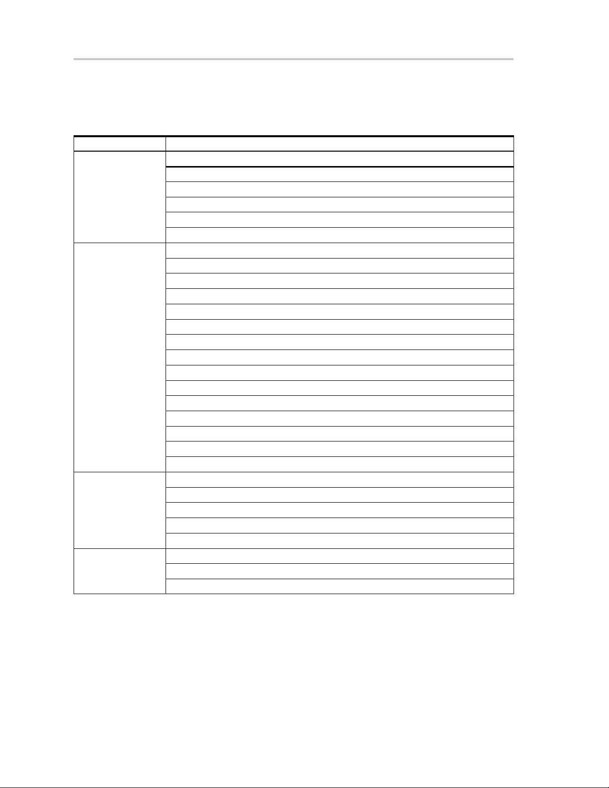
Tables
2–1 Function Buttons and Descriptions 2-4. . . . . . . . . . . . . . . . . . . . . . . . . . . . . . . . . . . . . . . . . . . . . .
2–2 Status Messages 2-5. . . . . . . . . . . . . . . . . . . . . . . . . . . . . . . . . . . . . . . . . . . . . . . . . . . . . . . . . . . . .
2–3 Error Messages 2-6. . . . . . . . . . . . . . . . . . . . . . . . . . . . . . . . . . . . . . . . . . . . . . . . . . . . . . . . . . . . . . .
2–4 Control Bit Definitions for Target Connector Pins 2-8. . . . . . . . . . . . . . . . . . . . . . . . . . . . . . . . . .
3–1 Data Frame of Firmware Commands 3-3. . . . . . . . . . . . . . . . . . . . . . . . . . . . . . . . . . . . . . . . . . . .
5–1 MSP-GANG430 Hardware Specifications 5-2. . . . . . . . . . . . . . . . . . . . . . . . . . . . . . . . . . . . . . . .
5–2 MSP-GANG430 Target Connector Signal Functions 5-5. . . . . . . . . . . . . . . . . . . . . . . . . . . . . . .
5–3 MSP-GANG430 Signal Levels 5-5. . . . . . . . . . . . . . . . . . . . . . . . . . . . . . . . . . . . . . . . . . . . . . . . . .
vi
Page 7

Chapter 1
Introduction, Installation, and Setup
This chapter introduces the MSP-GANG430 and guides you through the
installation of the software and hardware.
Topic Page
1.1 Introduction 1-2. . . . . . . . . . . . . . . . . . . . . . . . . . . . . . . . . . . . . . . . . . . . . . . . . .
1.2 Software Installation 1-3. . . . . . . . . . . . . . . . . . . . . . . . . . . . . . . . . . . . . . . . . .
1.3 Hardware Installation 1-3. . . . . . . . . . . . . . . . . . . . . . . . . . . . . . . . . . . . . . . . . .
Introduction, Installation, and Setup
1-1
Page 8

Introduction
1.1 Introduction
The MSP-GANG430 is an MSP430 device programmer that can program up
to eight MSP430 flash devices at the same time. The MSP-GANG430
connects to the host PC using a standard RS232 serial connection. The
MSP-GANG430 provides flexible device programming options as described
in Chapter 2.
The MSP-GANG430 is not a gang programmer in the traditional sense; there
are not eight sockets provided to program the target devices. Instead, the
MSP-GANG430 is designed to connect to the target devices in-circuit (i.e., the
target devices are mounted in the customer’s final circuit/system). The
MSP-GANG430 accesses the target devices using connectors to the JTAG
signals.
Chapter 6 contains a schematic that documents how the signals from the
MSP-GANG430 can be brought out to each of the target devices via an
MSP430-standard JTAG connector. The circuit could easily be modified to
connect the signals to the target device pins directly (via a socket) if a
traditional gang programmer was desired.
The MSP–GANG430 is provided with an expansion board that implements the
interconnections between the MSP–GANG430 and multiple target devices.
Eight cables are provided that connect the expansion board to eight target
devices (via a JTAG connector).
1-2
Page 9

1.2 Software Installation
To install the MSP-GANG430 software:
1) Insert the MSP430 CD-ROM into the CD-ROM drive of the computer. The
setup routine automatically opens the default browser of the computer and
displays the MSP430 start page. Alternatively, open the file index.htm
located in the root directory of the CD-ROM using a browser. The MSP430
start page is displayed in the browser window.
2) Select Tool Software
3) Select MSP-GANG430 Gang Programmer
4) Select Save this program to disk under the File Download options and click
OK. A Save As dialog is displayed.
5) Using the Save As dialog, save the GANG430_Rxxx.exe program to the
computer. Make a note of the directory path to this file.
6) Navigate to this file (GANG430_Rxxx.exe) and execute it. A welcome
message is displayed on the screen.
7) The setup program guides you through the installation process. Follow the
setup instructions on the screen.
Software Installation
8) On completion of the setup program execution, the MSP-GANG430
program icons are created in the selected folder. Click on the GANG430
Read Me First icon to obtain important information about the
MSP-GANG430 hardware and software.
9) The appropriate program group and icons are added to the Windows
program manager.
10) To start the MSP-GANG430 software, click the GANG430 icon in the
selected program group (the default program group is ADT430).
1.3 Hardware Installation
To install the MSP-GANG430 hardware:
1) Connect the MSP-GANG430 to the serial port (COM1–COM4 or
extension board) of the PC using the 9-pin SUB-D connector.
2) Connect an external power supply to the MSP-GANG430. The voltage of
the power supply must be between 8 V and 15 V dc and must be capable
of providing a minimum current of 300 mA. The center post of the power
supply connector on the MSP-GANG430 is the positive voltage terminal.
The power supply connection status is indicated by the yellow system LED
on the MSP-GANG430.
3) The expansion board should be attached to the 25-pin SUB-D connector
on the MSP–GANG430. It provides connectivity for up to eight targets, via
the included eight 14-pin cables. The target MSP430 flash devices can be
in standalone sockets or can be on an application’s PCB and are accessed
via the JTAG signals.
Introduction, Installation, and Setup
1-3
Page 10
Hardware Installation
Note: Maximum Signal Path Length: 60 cm
The maximum length of the signal path between the 25-pin SUB-D connector
on the MSP-GANG430 and a target device is 60 cm.
4) The MSP–GANG430 provides the selected power supply voltage V
(VCC_MSP on pins 7 and 14 of the 25-pin SUB-D target connector; pin
2 on the 14-pin cable) to the target devices in application PCBs. A maximum total current of 150 mA can be provided by the programmer to the
targets.
5) When an external supply voltage V
should also be fed into the sense input pin (MSP_VCC_IN on pin 15 of the
25-pin SUB-D target connector; pin 4 on the 14-pin cable) of the
programmer. This connection allows the integrated level shifters to match
the target JTAG signal levels with the external supply voltage.
When an external supply voltage is used for the target systems, it is very
important to disconnect VCC_MSP from the targets to avoid power supply
conflicts that could potential damage the MSP-GANG430 and the targets.
Connect the external supply voltage to MSP_VCC_IN.
It is not possible to use the MSP-GANG430 with targets powered by the
MSP-GANG430 and with targets powered by an external supply
simultaneously.
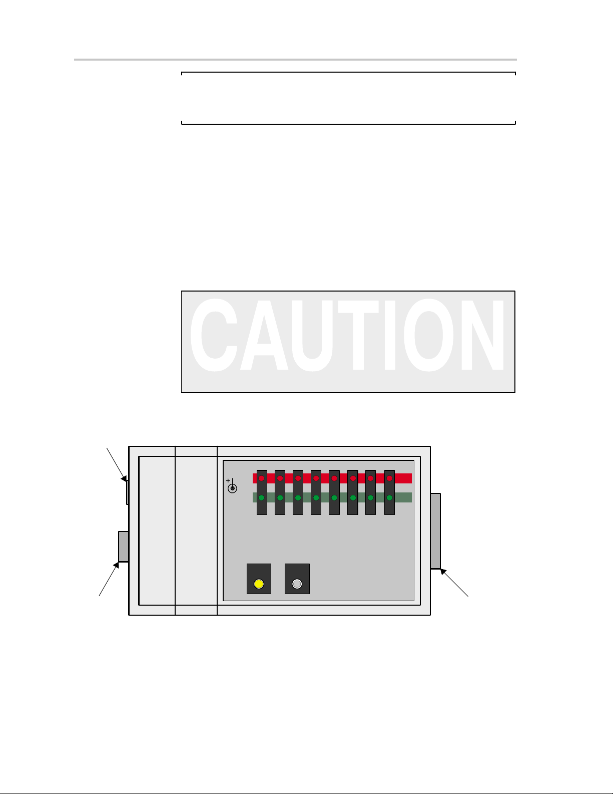
Figure 1–1.MSP-GANG430 Gang Programmer
Power
supply
is used for the target systems, it
CC
CC
RS232
from
PC
1-4
8–15 V
300 mA
RS232
MODE START
ERR
12345678
MSP430 Gang Programmer
MSP-GANG430
TI
OK
TARGET
JTAG connector
for eight
MSP430 devices
Page 11

Chapter 2
Operation
This chapter describes the various methods for programming MSP430 flash
devices using the MSP-GANG430.
Topic Page
2.1 Programming MSP430 Flash Devices Using the GUI 2-2. . . . . . . . . . . . .
2.2 Programming MSP430 Flash Devices in Standalone Mode 2-9. . . . . . . .
2.3 Programming MSP430 Flash Devices With User-Configured UART
Handler 2-9. . . . . . . . . . . . . . . . . . . . . . . . . . . . . . . . . . . . . . . . . . . . . . . . . . . . . .
2.4 Programming MSP430 Devices With GANG430.DLL 2-9. . . . . . . . . . . . . .
Operation
2-1
Page 12

Programming MSP430 Flash Devices Using the GUI
2.1 Programming MSP430 Flash Devices Using the GUI
2.1.1 Procedure
The following sequence must be followed to start the GUI and program
MSP430 flash devices using the MSP-GANG430:
1) Connect the MSP-GANG430 hardware and the targets as suggested in
Section 1.3.
2) Click on the GANG430 icon located in the program group specified during
installation of the software (default: ADT430). The MSP430 FLASH Gang
Programmer GUI is displayed on the screen (see Figure 2–1). The status
line in the GUI displays the message MSP-GANG430 Gang Programmer
connected. If this message is not displayed, check the CO
in the communication settings and the MSP-GANG430 connections.
M Port selection
3) Select the required device using the D
4) Select the object code file to be programmed into the device(s) using the
ame menu. The formats supported for the object code file are TI TXT
File N
(.txt) and Intel hex (.a43).
5) Use the L
sum to the MSP-GANG430. The data is written to an internal memory
called the image buffer.
6) Select the supply voltage using the Su
7) Select the options in Main Process as required.
8) Click on the S
operation. The progress and completion of the operation is displayed in
status.
oad Image button to download the object code file and its check-
tart button in Main Process to start the gang programming
evice Type menu.
pply Voltage menu.
2-2
Page 13
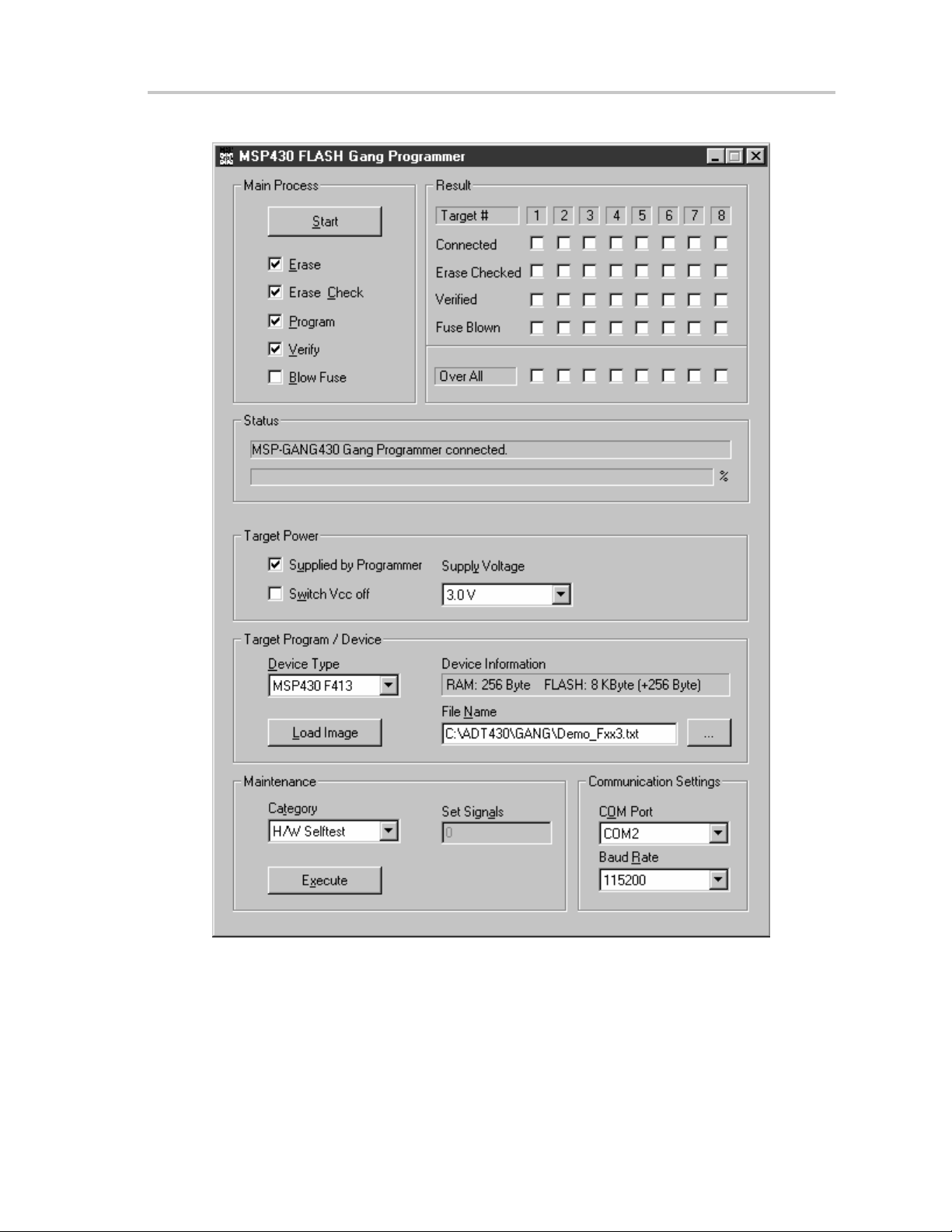
Figure 2–1.MSP-GANG430 GUI
Programming MSP430 Flash Devices Using the GUI
Operation
2-3
Page 14
Programming MSP430 Flash Devices Using the GUI
2.1.2 Description of the MSP-GANG430 GUI
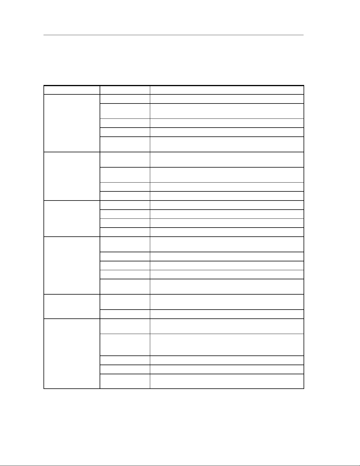
Table 2–1 describes the function buttons and option settings in the
MSP-GANG430 GUI.
Table 2–1.Function Buttons and Descriptions
Button–Group Functions Description
Start – Main Process
Executes the
function(s) selected
function(s) selected
in Main Process
Target Power
Load Image –Target
Program/Device
Execute –
Maintenance
Communication
Settings
System menu
Erase Erase all of the target’s flash memory (main and information)
Erase check Check that the target’s main and information flash memories are
erased
Program Program the image buffer into the target’s flash memory
Verify Compare the target’s flash memory and the image buffer
Blow fuse Blow the target’s JTAG fuse after successful completion of the
selected operations
Supplied by
programmer
Switch VCC off The supply voltage provided by the VCC_MSP pin is switched off
Supply voltage Select the voltage supplied to the targets
Settling Time Time to allow the target capacitors to fully charge
Load image Load the selected object code file into the image buffer .
Device Type Select the memory model of the target
Device Information Memory details of the selected device type
File name The file containing the object code
H/W self test Initiate hardware self test. All green LEDs on – test pass. All red
Update firmware Update MSP-GANG430 firmware with the firmware update file
Read out Target Read out exclusively one of eight target modules.
Erase image Erase the image buffer
Target connector
(test)
COM port Select the PC serial port used to communicate with the
Baud rate Select the baud rate of the serial port
System menu
mode
Lock settings All settings on the GUI are locked. Only the Start button, the Result
Unlock settings The locked settings and the hidden group boxes are enabled.
Help… Opens the user help window
About gang
programmer…
The connected targets are powered by the MSP-GANG430 via
VCC_MSP pin.
after programming the targets.
LEDs on – test fail.
Set the selected pin on the 25-pin target connector of the
MSP-GANG430.
MSP-GANG430.
The System Menu is displayed by clicking on the icon at the upper
left corner of GUI (or {Alt} and {Space} pressed together).
group box, and the Status group box are displayed. Other group
boxes are hidden.
Desktop application software and firmware version and filename
information is displayed
2-4
Page 15
2.1.3 Status Messages
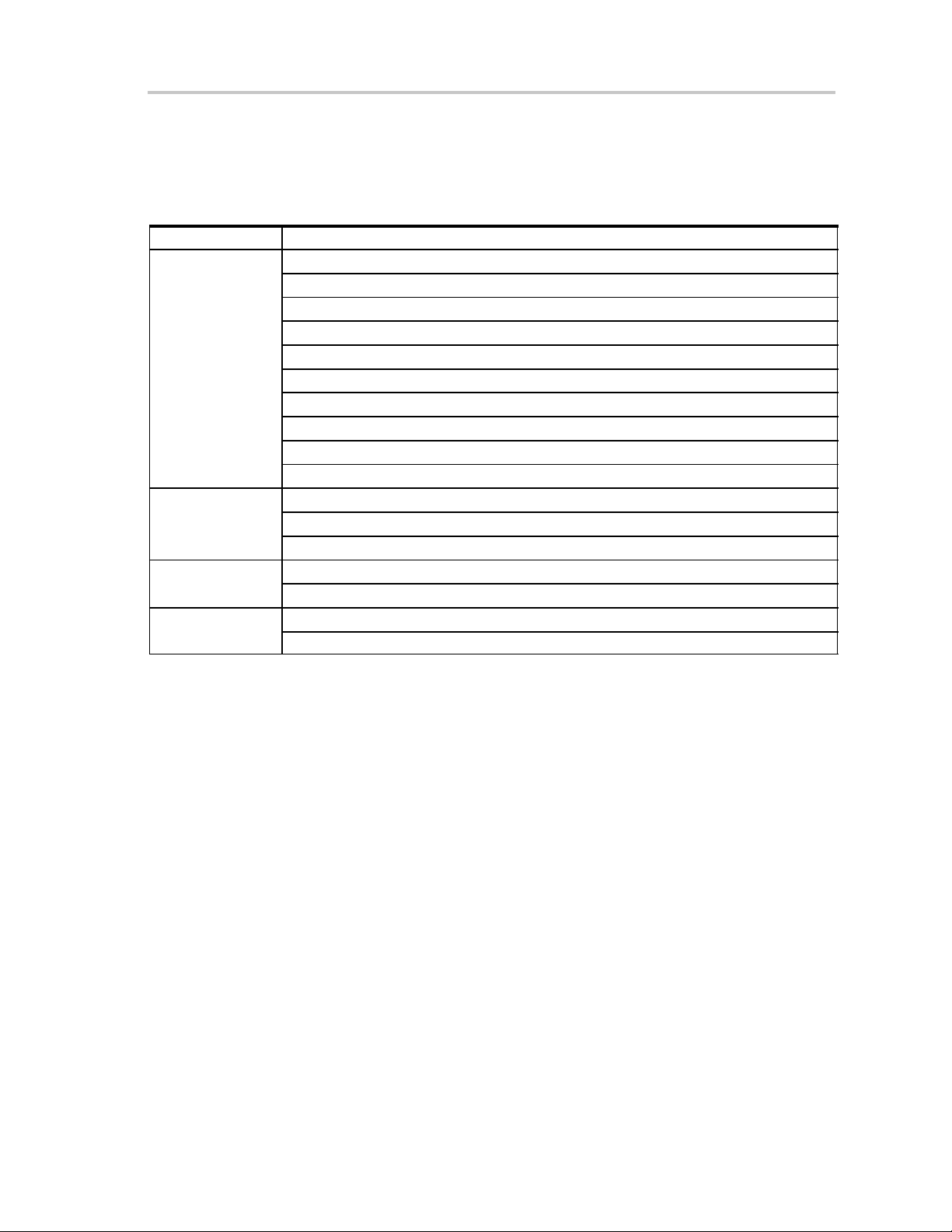
Table 2–2 shows the status messages that can be displayed in the
MSP-GANG430 GUI during operation.
Table 2–2.Status Messages
Status Type Status Messages
Progress
System
Setting
Maintenance
Executing main process...
Erasing image buffer ...
Loading image buffer ...
Loading checksum of image buffer ...
Erasing firmware section...
Loading firmware section...
Initializing firmware...
Changing baud rate...
Executing self test...
Setting signals at target connector...
Operation successful
MSP-GANG430 gang programmer connected.
Result of the operation: See the result section.
COM port settings modified. MSP-GANG430 gang programmer connected.
Target power settings modified
Operation successful
Selftest passed
Programming MSP430 Flash Devices Using the GUI
Operation
2-5
Page 16
Programming MSP430 Flash Devices Using the GUI
2.1.4 Error Messages
Table 2–3 shows the error messages that can be displayed in the
MSP-GANG430 GUI when an error occurs during operation.
Table 2–3.Error Messages
Error Type Error Message
Communication
Setting
System
System
Maintenance
Windows
ERROR: Unable to read Target!
ERROR: Unable to open COM port – already in use?
ERROR: Unable to close COM port!
ERROR: Synchronization failed. Programmer connected?
ERROR: Time out during operation – Correct COM port selected?
ERROR: Communication – Frame has errors!
ERROR: Select baud rate command not accepted!
WARNING: Target voltage too low for erase / program operation! Set to > 2.7–V.
WARNING: Could not set target voltage – Externally supplied?
ERROR: Value wrong or out of range!
ERROR: Selected file is of unrecognizable format!
ERROR: Selected file is not a firmware update file!
ERROR: Firmware section cannot be erased!
ERROR: Unable to load firmware. Correct file format?
ERROR: Unable to refresh gang programmer system parameters!
ERROR: Unable to load Image buffer! Image buffer erased? Correct file format?
ERROR: Result of operation not received!
FATAL ERROR: Image memory corrupted or erased!
ERROR: Unexpected end of file!
ERROR: File contains invalid record!
General error!
ERROR: Self test failed – No access to one ore more image buffer devices!
ERROR: Self test failed – No JTAG access to one or more target channels!
ERROR: Self test failed – Target voltage generator (V
ERROR: Self test failed – system voltage (VCC) not in range!
ERROR: Self test failed – blow fuse voltage (VPP) not in range!
ERROR: Unable to open file!
ERROR: Error during file I/O!
ERROR: Unable to open INI file!
) does not work properly!
CCT
2.1.5 Description of the Gang430.ini File
The Gang430.ini file contains the MSP-GANG430 default settings and the last
used GUI settings.
2.1.5.1 Section [System]
The last used settings of the MSP-GANG430 GUI are stored in the
Gang430.ini file before exiting the GUI application program. This information
is stored under the [System] section of the file.
2-6
Page 17

2.1.5.2 Section [User]
The initial settings for the following parameters are in the [User] section and
may be modified by the user:
CaptionIndexed = 0 (default)
The caption of the MSP-GANG430 GUI in the default state is MSP430 FLASH
Gang Programmer.
When CaptionIndexed = 1, the caption is extended with a suffix [n] to allow
multiinstance operation for programming in automated production
environment that uses caption titles for process control. The suffix n
represents the unique COMn port number for that instance. E.g. for COM3, the
caption is displayed as MSP430 FLASH Gang Programmer [3].
2.1.5.3 Section [Timing]
The [Timing] section shows the approximate time that has elapsed in
milliseconds for various operations of the MSP-GANG430. The parameters
under this section are updated after the associated operations are successful.
The information on the elapsed time is useful for development and setup. The
parameter that is most interesting is the time taken to complete a gang
programming cycle, represented by TimeGangProg under this section.
Programming MSP430 Flash Devices Using the GUI
2.1.5.4 Section [Diagnostic]
The [Diagnostic] section is useful for automatic production using the
MSP-GANG430. During gang programming operation, Busy = 1. After
completion of the operation, the information in the Result group box in the GUI
is also listed in this section for the following: Connected, EraseChecked,
Verified, FuseBlown, OverAll, and MiscErrors, if any. A Busy = 0 terminates
that process and the diagnostics can be read from the .ini file.
For Example:
OverAll=239 (hexadecimal 0xEF) means: All channels except channel 5
were successfully processed (channel 1 represents the LSB, channel 8
represents the MSB of a byte).
Note:
When MiscErrors is nonzero, the diagnostic values are not valid for evaluation. Possible values for MiscErrors are shown below.
MiscErrors Description
0
1 FATAL ERROR: Image memory could be corrupted or
Operation successful
erased
11 ERROR: Main process parameters not yet set
16
ERROR: Could not set target voltage (VCCT) –
MSP_VCC_IN pin connected?
Operation
2-7
Page 18

Programming MSP430 Flash Devices Using the GUI
2.1.6 Target Connector Functional Check
The MSP-GANG430 GUI diagnostics support a functional check of the target
connector pins. The functional check is invoked by selecting the Target
Connector category in the Maintenance group box, and clicking the Execute
button with the appropriate Set Signals defined. The Set Signals value is the
decimal value that represents the combination of the appropriate control bits.
The defined pin’s signal level is available for measurement after execution of
the functional check. The signal levels remain unchanged until another
configuration is set. The target connector functional check must always be
terminated by executing the End of Check setting (0x8000 = 32768) or by
executing an H/W self test to initialize the MSP-GANG430. Table 2–4 shows
the details of the control bits.
Table 2–4.Control Bit Definitions for Target Connector Pins
Bits Pin Function and Levels Signal Level Connector Pins
0x0000 Select TDO/TDI1 – 1,8
0x0001 Select TDO/TDI2 – 9
0x0002 Select TDO/TDI3 – 10
0x0003 Select TDO/TDI4 – 11
0x0004 Select TDO/TDI5 – 12
0x0005 Select TDO/TDI6 – 13
0x0006 Select TDO/TDI7 – 25
0x0007 Select TDO/TDI8 – 24
0x0008 Logic level at TDO/TDIx pin
Logic level at TDI/VPP pin
0x0010 Logic level at TCK pin VCC or 0 4
0x0020 Logic level at TMS pin VCC or 0 3
0x0040 Logic level at TEST/VPP pin VCC –0.25V or 0 17
0x0080 Logic level at TDI/VPP pin VCC or 0 2
0x0100 VCC on/off at VCC_MSP pin VCC or 0 7, 14
0x0200 VPP on/off at TDI/VPP pin, overwrites bit 0x0080 VPP or 0 2
0x0400 VPP on/off at TEST/VPP pin VPP or 0 17
0x7800 Reserved
0x8000 End of check, reinitialize MSP-GANG430 initial all
VCC or 0
V
/VPP or 0
CC
1, 8–13, 25, 24,
2
2-8
Example:
To check the logic high level on TDO/TDI3 and VPP voltage level on
TEST/VPP:
Enter 1034 (0x0002 + 0x0008 + 0x0400) into Set Signal and click Execute.
The V
at pin 10 and VPP at pin 17 can be measured now. All other pins
CC
remain at 0 V. The connector case is electrically grounded, as are pins
19–23.
Page 19

Programming MSP430 Flash Devices in Standalone Mode
2.2 Programming MSP430 Flash Devices in Standalone Mode
The MSP-GANG430 supports a standalone mode of programming the target
MSP430 flash devices.
The programming options for the MSP-GANG430 while operating in
standalone mode are configured using the GUI. When the Start button in Main
Process is clicked, all selected options are downloaded into the flash memory
of the MSP-GANG430. Once the download is complete, the MSP-GANG430
can be disconnected from the PC and used standalone to program the target
devices. The START push-button on the MSP-GANG430 operates identical
to the Start button of the GUI. Progress of the operation in standalone mode
is indicated by the flashing yellow LED.
The result status is represented by the rows of green and red LEDs on the
MSP-GANG430. For each channel, a green LED indicates a successful
operation and a red LED indicate a failed operation. If both red and green LEDs
are off for a channel, the target device connected to that channel is not
accessible or is not connected.
In standalone mode, the H/W self test of the MSP-GANG430 can be initiated
by pressing the ST ART key for more than three seconds. The progress of the
test is indicated by alternate flashing of green and red LEDs in groups of four.
Upon completion of the self test, all eight green LEDs are on if the self test
passes. Any other combinations of the LEDs indicate a failed self test.
2.3 Programming MSP430 Flash Devices With User-Configured UART
Handler
The MSP-GANG430 programmer supports programming the MSP430 flash
devices by using generic firmware commands. The generic firmware
commands and protocol are described in Chapter 3.
2.4 Programming the MSP430 Devices With GANG430.DLL
The MSP–GANG430 programmer supports programming the MSP430 flash
devices by using DLL functions. The usage of the DLL functions and their
prototypes (calling conventions) are described in Chapter 4: Dynamic Link
Library GANG430.DLL.
Operation
2-9
Page 20

2-10
Page 21

Chapter 3
Firmware
This chapter describes the firmware commands and protocol for controlling
the MSP-GANG430 via its RS-232 serial communication interface.
Topic Page
3.1 Commands 3-2. . . . . . . . . . . . . . . . . . . . . . . . . . . . . . . . . . . . . . . . . . . . . . . . . . .
3.2 Firmware Interface Protocol 3-2. . . . . . . . . . . . . . . . . . . . . . . . . . . . . . . . . . .
3.3 Synchronization Sequence 3-2. . . . . . . . . . . . . . . . . . . . . . . . . . . . . . . . . . . .
3.4 Data Frame 3-2. . . . . . . . . . . . . . . . . . . . . . . . . . . . . . . . . . . . . . . . . . . . . . . . . . .
3.5 Commands—Detailed Description 3-4. . . . . . . . . . . . . . . . . . . . . . . . . . . . . .
Firmware
3-1
Page 22

Commands
3.1 Commands
The MSP-GANG430 can be controlled via firmware commands received on
its RS-232 serial port.
The following firmware commands are supported:
- Load Parameters
- Start
- Transmit Diagnostics
- Erase Image
- Load Image Block
- Load Image Checksum
- Erase Firmware
- Load Firmware Block
- Finalize Firmware
- Select Baud Rate
- Execute Self Test
- Set Signals (at target connector)
- Read Target Selective
- Write Target Selective
- Set Target Vcc
3.2 Firmware Interface Protocol
The MSP-GANG430 supports the following UART communication protocol:
- Baud rates from 9600 to 115200 baud in half duplex mode. The default
baud rate at startup is 1 15200 baud, and is the recommended baud rate.
- One start bit, eight data bits, even parity bit, and one stop bit.
- Software handshake by (not)acknowledge character.
3.3 Synchronization Sequence
To synchronize with the MSP-GANG430, the host serial handler transmits a
SYNC character (80h) to the MSP-GANG430. The MSP-GANG430 acknowledges successful reception of the SYNC by responding with a DATA_ACK
character (0x90). If the SYNC is not received correctly , a DAT A_NAK character
(0xA0) is sent back. This sequence is required to establish the communication
channel and/or react immediately to line faults.
Note:
The synchronization character is not part of the data frame described later
in this chapter.
3.4 Data Frame
The data frame format used follows the TI MSP430 serial standard protocol
(SSP) rules extended with a preceding synchronization sequence (SS), as
previously described. The MSP-GANG430 is considered the receiver in
Table 3–1.
3-2
The obvious redundancy of some parameters results from the adaptation of
the SSP, or to save boot ROM space.
Page 23

3.4.1 Frame Structure
The data frame format of the firmware commands is shown in Table 3–1:
- The first 8 bytes (HDR through LH) are mandatory (xx represents dummy
- Data bytes D1 to Dn are optional.
- Two bytes (CKL and CKH) for checksum are mandatory.
- Acknowledge done by the MSP-GANG430 is mandatory except with the
3.4.2 Checksum
The 16-bit (2 bytes) checksum is calculated over all received/transmitted bytes
B1 … Bn in the data frame except the checksum bytes themselves by XORing
words (2 successive bytes) and inverting the result.
Formula:
or
Data Frame
data).
transmit diagnostic command.
CHECKSUM = INV [ (B1 + 256 x B2) XOR (B3 + 256 x B4) XOR … XOR
(Bn – 1 + 256 x Bn) ]
CKL = INV [ B1 XOR B3 XOR … XOR Bn–1 ]
CKH = INV [ B2 XOR B4 XOR … XOR Bn ]
Table 3–1.Data Frame of Firmware Commands
Received
MSP-GANG430
Firmware Command
Load Parameters 80 36 06 06 D1 D2 D3 D4 D5 D6 CKL CKH ACK
Start 80 31 04 04 00 00 00 00 — — CKL CKH ACK
Transmit Diagnostic 80 32 04 04 00 00 00 00 — — CKL CKH —
GANG430 responds 80 00 1E 1E D1 D2 D3 D4 D5 D06…D1E CKL CKH —
Erase Image 80 33 04 04 00 00 00 00 — — CKL CKH ACK
Load Image Block 80 34 n n AL AH n–4 00 D1 D2…Dn–4 CKL CKH ACK
Load Image Checksum 80 37 06 06 D1 D2 D3 D4 D5 D6 CKL CKH ACK
Execute Self test 80 35 04 04 00 00 00 00 — — CKL CKH ACK
Set Signals 80 30 04 04 D1 D2 D3 D4 — — CKL CKH ACK
Erase Firmware 80 39 04 04 D1 D2 D3 D4 — — CKL CKH ACK
Load Firmware Block 80 3A n n AL AH n–4 00 D1 D2…Dn–4 CKL CKH ACK
Finalize Firmware 80 3B 04 04 00 00 00 00 — — CKL CKH ACK
Select Baud Rate 80 38 04 04 D1 D2 D3 D4 — — CKL CKH ACK
Write Target Selective 80 3C n n AL AH n–4 00 D1 D2…Dn–4 CKL CKH ACK
Read Target Selective 80 3D 06 06 AL AH n 00 D1 D2 CKL CKH —
GANG430 responds 80 00 n n D1 D2 D3 D4 D5 D6…Dn CKL CKH —
Set Target V
Note: All numbers are bytes in hexadecimal notation.
Abbreviations:
HDR DATA_FRAME = 0x80 means data frame expected in accordance with TI MSP430 serial standard protocol
CMD Command identification
CC
ACK is sent back by the MSP-GANG430.
The synchronization sequence is not part of the data frame.
(SSP).
H
C
D
M
R
80 3E 04 04 D1 D2 D3 D4 — — CKL CKH ACK
L1 L2 AL AH LL LH D1 D2 … Dn
D
C
C
K
K
L
H
A
C
K
Firmware
3-3
Page 24

Commands—Detailed Description
L1, L2 Number of bytes consisting of AL through Dn
AL, Ah Block start address or erase (check) address or jump address LO/HI byte
LL, LH Number of pure data bytes (max. 250) or erase information LO/HI byte or block length of erase check (max.
D1 . . . Dn Data bytes
CLK, CKH 16-bit checksum LO/HI byte
xx Can be any data
— No character (data byte) received/transmitted
ACK The acknowledge character returned by the MSP-GANG430, can be either
n Number of bytes
Restrictions: L1 = L2, L1 < 255, L1 even.
FFFFh)
DATA_ACK = 0x90: Frame was received correctly, command was executed successfully, or
DAT A_NAK = 0xA0: Frame not valid (e.g., wrong checksum, L1 ≠ L2), command is not defined, is not allowed,
or was executed unsuccessfully.
3.5 Commands—Detailed Description
3.5.1 General
Besides the header byte HDR (0x80) and the command identification CMD,
the frame length bytes L1 and L2 (which must be equal) hold the number of
bytes following L2, excluding the checksum bytes CKL and CKH.
Bytes AL, AH, LL, LH, D1…Dn are command specific. However , the checksum
bytes CKL (low byte) and CKH (high byte) are mandatory.
If the data frame has been received correctly and the command execution was
successful, an acknowledge character DA T A_ACK = 0x90 is sent back by the
MSP-GANG430. Incorrectly received data frames, unsuccessful operations,
commands which are not defined are confirmed with a DATA_NAK = 0xA0.
3.5.2 Load Parameters
The load parameters command is used to download the information the main
process needs for gang programming to the MSP-GANG430. It has to be invoked prior to the first gang programming command. The parameters are
stored in the system flash memory.
Data bytes D1 to D6 hold the parameters as follows:
D1 Flags for process control, in any combination:
D2 Flags for target supply voltage VCC_MSP:
D3, D4 Reserved
0x03: Mass Erase
0x0C: Program
0x10: Erase Check
0x20: Verify
0x40: Blow Fuse
0x3F: Voltage in 100-mV steps (allowed are 18…36, 0 for external
supply)
0x80: Switch VCC_MSP off after programming
3-4
D5, D6 VCC_MSP settle time:
Delay in milliseconds between switching VCC_MSP on and starting
programming cycle. Valid values are 1…0xFFFF (>65s).
D5 holds the LSB, D6 the MSB
Page 25

3.5.3 Start
The start command executes the gang programming cycle. The operations
are defined with the load parameters command. The result of the command
execution can be determined using the transmit diagnostic command
described below.
3.5.4 Transmit Diagnostic
The transmit diagnostic command provides the result of the preceding gang
programming command.
Data bytes D1 to D1E hold the parameters as follows:
D1 to D5 give information about success of each target channel. The LSB
represents channel 1, the MSB represents channel 8:
D1 Channels which are connected to the programmer (device detected).
D2 Channels which passed the erase check successfully.
D3 Channels which passed the verification successfully.
D4 Channels which passed the blow fuse successfully, fuse already
blown.
D5 Channels which passed all operations successfully.
D6 Miscellaneous errors. See the Section [Diagnostic] paragraph.
D7 to D8 are reserved.
D9 to D10 hold the hardware version number: D9 (MSByte), D10
(LSByte).
D11 to D12 hold the firmware version number: D11 (MSByte), D12
(LSByte).
D13 to D30 hold a zero terminated character string representing the firm-
ware file name e.g. GANG430_100.TXT.
Commands—Detailed Description
3.5.5 Erase Image
The erase image command erases the entire image memory and verifies the
erasure.
3.5.6 Load Image Block
The load image block command loads the data bytes into the image buffer of
the MSP-GANG430, and verifies them.
D1 to Dn–4 contains the data bytes.
3.5.7 Write Target Selective
The write target selective command loads the data bytes into one exclusively
selected target flash memory and verifies them.
Before applying this operation stable supply voltage at the targets is assumed
(if not, use Set T arget V
time).
command and optionally wait for capacitor’s settle
CC
Firmware
3-5
Page 26

Commands—Detailed Description
D1 Target number (0..7)
D2 0
D3 to Dn–4 contain the data bytes (start address and number of bytes
3.5.8 Read Target Selective
The read target selective command is used for any read access to the flash
memory/RAM or peripheral module control registers at 0100h–01FEh of the
selected target.
The 16-bit block start address is defined in AL (low byte) and AH (high byte).
The 16-bit block length is defined in LL (low byte) and LH (high byte). Because
pure data bytes are limited to a maximum of 250, LH is always 0.
For this operation stable supply voltage at the targets is necessary . Iif not, use
Set Target VCC command and wait for capacitor’s settle time as required.
D1 Target number (0..7)
D2 0
The GANG430 responds with the requested data block. No acknowledge
character is necessary.
D1 to Dn contain the data bytes (start address and number of bytes must
must be even numbered).
be even numbered).
3.5.9 Set Target V
CC
The Set Target VCC command sets the VCC_MSP pin voltage of the
programmer’s target connector to the given value.
D1 Target supply voltage:
0 VCC_MSP output voltage is equal to MSP_VCC_IN input
voltage
1 VCC_MSP output voltage is switched off
2 VCC_MSP output voltage is same as loaded by the Load
Parameters command
18+ VCC_MSP is set in hundreds of millivolts (e.g. D1 = 36 for
3.6 V)
D2 to D4 are 0x00.
3-6
Page 27

3.5.10 Load Image Checksum
The load image checksum command writes the checksum of the entire image
buffer and the memory model of the target device into the system flash
memory. The gang programmer uses the checksums to verify the correct
download of data to the image buffer and the correct programming of the target
device.
Data bytes D1 to D6 hold the parameters as follows:
D1 0x7F: Memory models 0 to 9 (10 … 127 for future use).
0x80: VPP to TEST; 0x00 VPP to TDI.
D2 Reserved.
D3 Checksum (PSA) for information memory, LSByte
D4 Checksum (PSA) for information memory, MSByte
D5 Checksum (PSA) for main memory, LSByte
D6 Checksum (PSA) for main memory, MSByte
The pseudo signature analysis (PSA) is computed using the following
algorithm (using the C language):
Commands—Detailed Description
Where StartAddr is the beginning address of the memory region and Length
is the length of the memory region, data, in words.
3.5.11 Select Baud Rate
The select baud rate command sets the rate of the serial communications. The
default is 115200 baud.
Data bytes D1 to D4 hold the parameters as follows:
for (PSA = StartAddr – 2, i = 0; i < Length; i++)
{
if (PSA & 0x8000)
PSA = ((PSA ^ 0x0805) << 1) | 1;
else
PSA <<= 1;
PSA ^= Data[i];
}
D1 Baud rate index 0 to 4 representing
0: 9600 baud
1: 19200 baud
2: 38400 baud
3: 57600 baud
4: 115200 baud
D2 to D4 are 0x00.
The select baud rate command takes effect (i.e., changes the baud rate)
immediately.
Firmware
3-7
Page 28

Commands—Detailed Description
3.5.12 Execute Self Test
The execute self test command performs a test of the MSP-GANG430
hardware. In the event of failure, the MSP-GANG430 transmit diagnostic
command can be used to obtain detailed information about the failure. D6
(miscellaneous errors) holds the following error codes:
0x04 Self test failed – Control connections to image buffer devices invalid
0x05 Self test failed – No JTAG access to one or more target channels
0x06 Self test failed – target voltage generator (VCCT) does not work
0x07 Self test failed – System voltage (V
0x08 Self test failed – Blow fuse voltage (VPP) not in range
3.5.13 Set Signals
Data bytes D1 to D4 hold the parameters as follows:
See the target connector functional check paragraph.
D1 Control bits low byte
D2 Control bits high byte
D3 VCC voltage in hundreds of mV (18 to 36 represent 1.8 V to 3.6 V)
D4 0x00
properly
) not in range
CC
3.5.14 Firmware Commands
Commands which affect the firmware such as Erase Firmware, Load
Firmware Block, and Finalize Firmware are not recommended to be invoked
from other than the MSP-GANG430 GUI.
3-8
Page 29

Chapter 4
Dynamic Link Library GANG430.DLL
This chapter discusses the dynamic link library GANG430.DLL.
Topic Page
4.1 GANG430.DLL Description 4-2. . . . . . . . . . . . . . . . . . . . . . . . . . . . . . . . . . . . .
4.2 Return Values/Error Codes From the GNAG430.DLL 4-8. . . . . . . . . . . . .
Dynamic Link Library GANG430.DLL
4-1
Page 30

GANG430.DLL Description
4.1 GANG430.DLL Description
The GANG430.dll is used to communicate with the MSP–GANG430 programmer unit and the
connected MSP430 device(s).
The configuration of the MSP–GANG430 should be done with the following sequence:
InitCom // Open communication port
GangEraseImage // Erase image flash memory
GangLoadImage // Write target code into image flash memory
GangLoadParameters // Determine process flow
ReleaseCom // Close communication port
Once the configuration is completed all process specific parameters are stored in the flash memory of
the MSP–GANG430 programmer unit.
The subsequent gang programming process could be done as follows:
InitCom // Open communication port
GangSelectBaudrate // Optional: slow down communication speed
…GangMainProcess // Execute gang programming process
…GangGetResult // Receive result for diagnostic
…GangAccessTargetSFR // Optional: stimulate device pins
…GangProgramTarget // Optional: write serial numbers to targets
ReleaseCom // Close communication port
Several examples showing how the DLL could be used are located in the DLL_Usage_Examples
subdirectory of the GANG430 system. Every function returns an error code listed in the consecutive
paragraph.
This dll could be used separately using the following conventions:
InitCom
long int InitCom(char* lpszComPort, long int lBaudRate)
InitCom initializes (opens) the given communications port, establishes communication with the MSP-
GANG430 hardware, and sets the baud rate of the MSP–GANG430. If successful, the MSP–
GANG430 is reset.
lBaudRate: Valid baud rates are: 9600, 19200, 38400, 57600, and 115200 Baud. The default baud
rate after initialization is 115200 baud.
lpszComPort: The name of the communication port – COM1, COM2, COM3, or COM4
Example:
lFuncReturn = InitCom(“COM1”, 115200);
ReleaseCom
long int ReleaseCom (void)
This function is the counterpart to InitCom. It allows closing a communication with the MSP–
GANG430 hardware.
Example:
IFuncReturn = ReleaseCom();
4-2
Page 31

GANG430.DLL Description
GangSelectBaudrate
long int GangSelectBaudrate(long int lBaudrateIndex)
Sets the baud rate of the MSP–GANG430 programming unit. It offers the capability of transmissions
at lower baud rates than the default 115200 baud.
lBaudrateIndex:
0: 9600 Baud
1: 19200 Baud
2: 38400 Baud
3: 57600 Baud
4: 115200 Baud (default after power up)
Example:
lFuncReturn = GangSelectBaudrate(2); // selects 38400 Baud
GangEraseImage
long int GangEraseImage(void)
Clears (presets with 0xFF) the image memory of the MSP–GANG430 programming unit.
Performs a succeeding erase check over the address range 0x1000 to 0xFFFF.
Example:
lFuncReturn = GangEraseImage();
GangLoadImage
long int GangLoadImage(char* lpszFileName, char* lpszDeviceName)
This function writes data from a file either of type TI–txt or of type Intel-hex (auto-detect) into the
MSP-GANG430 programming unit’s image flash memory. It also writes the memory model
parameters of the selected device type and the checksums for main and information memory into the
programmer’s flash system memory.
lpszFileName: Name of the file to be loaded (full path).
lpszDeviceName: Name of the device in file Gang430.ini. T ake care of the <space> between MSP430
and Fxxx.
Example:
lFuncReturn = GangLoadImage(FileName, “MSP430 F1121A”); with ’’”
GangLoadParameters
long int GangLoadParameters(long int lFlags, long int lSupply, long int lVccSettleTime)
The GangLoadParameters function is used to download the information the main process needs
for gang programming to the MSP–GANG430. It has to be invoked prior to the first
GangMainProcess call. The parameters are stored in the system flash memory.
lFlags:
F_ERASE_INFO 0x01 // executes erasure of info memory
F_ERASE_MAIN 0x02 // executes erasure of main memory
F_ERASE_MASS 0x03 // executes erasure of info and main memory
Dynamic Link Library GANG430.DLL
4-3
Page 32

GANG430.DLL Description
F_PROGRAM_INFO 0x04 // executes programming of info memory
F_PROGRAM_MAIN 0x08 // executes programming of main memory
F_PROGRAM_MASS 0x0C // executes programming of info and main memory
F_ERASE_CHECK 0x10 // executes erase check of info and/or main memory
F_VERIFY 0x20 // executes verification of info and/or main memory
F_BLOW_FUSE 0x40 // executes fuse blowing
lSupply:
0x7F: Supply voltage VCC_MSP in hundreds of millivolts (30 –> 3.0V).
0x80: Switch VCC_MSP off after main process execution (symbolic F_VCC_OFF=0x80).
lVccSettleTime: Capacitor settle time in milliseconds, max 0xFFFF –> >65s.
Example:
lFuncReturn = GangLoadParameters(0x3F, 30, 100);
// executes Mass Erase, Erase Check, Mass Program, Verification; VCC_MSP = 3 V, VCC_MSP
settle time is 100 ms.
GangMainProcess
long int GangMainProcess(long int lTimeout)
This function executes the main process determined by the parameters loaded through the Gang-
LoadParameters function. Use a succeeding GangGetResult call to receive the result of the executed
main process.
lTimeout: The time out in hundreds of milliseconds until the programming unit must respond.
Example:
lFuncReturn = GangMainProcess(120); // with 12s time out
GangGetResult
long int GangGetResult(void *lpData)
This function reads out the result of the precedent execution of the main process at the
MSP–GANG430 programming unit.
It also can be used to get detailed error information about the precedent execution of some other
functions like GangSelftest.
lpData: Pointer points to a buffer that receives the result data.
Data bytes D00 to D29 hold the parameters as follows:
D0 to D4 give information about success of each target channel. The LSB represents channel 1 the
MSB represents channel 8:
D00 Channels which are connected to the programmer (device detected).
D01 Channels which passed the erase check successfully.
D02 Channels which passed the verification successfully.
D03 Channels which passed the blow fuse successfully, fuse already blown.
D04 Channels which passed all operations successfully.
D05 Miscellaneous errors. See paragraph Description of the GANG430.ini file /
Section[Diagnostic].
D06 to D07 are reserved.
4-4
Page 33

GANG430.DLL Description
D08 to D09 hold the hardware version number: D08 (MSByte), D09(LSByte).
D10 to D11 hold the firmware version number: D10 (MSByte), D11(LSByte).
D12 to D29 hold a zero terminated character string representing the firmware file name e.g.
GANG430–120.TXT.
Example:
lFuncReturn = GangGetResult(lpBuffer);
GangAccessTargetSFR
Long int GangAccessTargetSFR(long int lTarget, long int iFlags, long int lAddress, void* lpData)
Accesses one byte or word within the special function register area (SFR) of one selectable target.
The user has to take care about the memory attributes. Read access also can be used over the entire
address range.
The first (last) access must be additionally se to the SFR_START (SFR_STOP) flag.
Before applying this operation stable supply voltage at the targets is assumed (if not, use
GangSetVccTarget operation and optionally wait for capacitor’s settle time).
lTarget: The target number – 1 (resp. target 1..8 at programmer unit)
lFlags:
SFR_READ 0x00 read access
SFR_WRITE 0x01 write access, all targets are affected
SFR_START 0x02 start sequence (stop watchdog, halt CPU)
SFR_STOP 0x04 stop sequence (release CPU)
lAddress: Address of memory to be accessed. If address is lower than 0x0100 byte access is performed, word access otherwise.
lpData: Pointer points to a buffer that holds the data to be read/written.
Example:
lFuncReturn = GangAccessTargetSFR(7, 0, 0x120, &lpData);
// reads WDTCTL register of target 8 wordwise to lpData.
GangProgramTarget
long int GangProgramTarget(long int lTarget, long int lStart, long int lLength, void *lpData)
Programs data exclusively into the flash memory of one selectable target. It is mainly used for giv-
ing away serial numbers.
Before applying this operation stable supply voltage at the targets is assumed (if not, use Gang-
SetVccTarget operation and optionally wait for capacitor’s settle time).
lTarget: The target number – 1 (resp. target 1..8 at programmer unit)
lStart, lLength: Startaddress of destination memory and number of bytes (both must be even).
lpData: Pointer points to a buffer that holds the data to be programmed (the source data buffer).
Example:
lFuncReturn = GangProgramTarget(7, 0x1000, 0x10, lpData);
// programs 16 bytes exclusively into target 8 starting at address 0x1000.
GangReadTarget
long int GangReadTarget(long int lTarget, long int lStart, long int lLength, void *lpData);
Reads out data exclusively from one selectable target device into a buffer.
Dynamic Link Library GANG430.DLL
4-5
Page 34

GANG430.DLL Description
Before applying this operation stable supply voltage at the targets is assumed (if not, use
GangSetVccTarget operation and optionally wait for capacitor’s settle time).
lTarget: The target number – 1 (resp. target 1..8 at programmer unit)
lStart: Start address of the area to be read out (must be even). Allowed values: 0x0100 – 0xFFFE
(see memory map of the corresponding device).
lLength: Length of the area (must be even). Allowed values: 0x0000 – 0xFFFE (see memory map
of the corresponding device).
lpData: Pointer points to a buffer the data to be written to (the destination data buffer).
Example:
lFuncReturn = GangReadTargetFile(0, 0xF000, 0x1000, lpDest);
// reads 4k bytes exclusively from target 1 starting at address 0xF000 into a buffer.
GangReadTargetFile
long int GangReadTargetFile(long int lTarget, long int lStart, long int lLength, char* lpszFileName,
long int iFileType);
Reads out data exclusively from one selectable target device into a file either of type TI-txt or of
type Intel-hex.
Before applying this operation stable supply voltage at the targets is assumed (if not, use
GangSetVccTarget operation and optionally wait for capacitor’s settle time).
lTarget: The target number – 1 (resp. target 1..8 at programmer unit)
lStart: Start address of the area to be read out (must be even). Allowed values: 0x0100 – 0xFFFE
(see memory map of the corresponding device).
lLength: Length of the area (must be even). Allowed values: 0x0000 – 0xFFFE (see memory map
of the corresponding device).
lpszFileName: Name of the file (full path) to receive data. If the file does not exist, it will be
created; if the file already exists, it will be overwritten.
iFileType:
FILETYPE_TI_TXT 0x01 file type is TI-txt
FILETYPE_INTEL_HEX 0x02 file type is Intel-hex
Example:
lFuncReturn = GangReadTargetFile(7, 0xF000, 0x1000, FileName, 1);
// reads 4k bytes exclusively from target 8 starting at address 0xF000 into a file with TI-txt format.
GangSetVccTarget
long int GangSetVccTarget(long int lVoltage)
This function sets the VCC_MSP pin voltage of the programming adapter’s target connector to the
given value.
lVoltage:
VCC_EXT 0 VCC_MSP output voltage is equal to MSP_VCC_IN input voltage
VCC_OFF 1 VCC_MSP output voltage is switched off
VCC_NOM 2 VCC_MSP output voltage is same as loaded by the GangLoadParameters
function.
Others 18+ VCC_MSP is set in hundreds of millivolts
Example:
lFuncReturn = GangSetVccT arget(36); // Set target V
4-6
to 3.6 V
CC
Page 35

GANG430.DLL Description
GangSelftest
Long int GangSelftest(long int lTimeout)
GangSelftest performs a self test at the MSP–GANG430 programmer unit. Use a succeeding Gang-
GetResult call to receive the result of the executed self test.
For detailed information about possible errors, refer to the Firmware/Execute Self Test paragraph.
lTimeout: The time out in hundreds of milliseconds until the programming unit must respond.
Example:
lFuncReturn = GangSelftest(60); // with 6s time out
GangSetSignals
long int GangSetSignals(long int lSignals, long int lVoltage)
Sets specified signals at the MSP–GANG430 programmer unit’s target connector.
For detailed information about bit definitions, see the Operation/Target Connector Functional Check
paragraph.
lSignals: Determines output signals.
lVoltage: Determines logic high level voltage of signals in hundreds of millivolts.
Example:
lFuncReturn = GangSetSignals(0x0400, 27);
// V
at pin 17 (TEST/VPP); VCC = 2.7V
PP
InitProgress
long int InitProgress(long int hStatusWnd, long int hProgBar)
Passes the handles of the status window and the progress bar of the front end application. It offers
the capability of updating a status window and/or a progress bar e.g. during file I/O operations.
hStatusWnd: Window handle of a status line.
hProgBar: Window handle, esp. of a progress bar.
Example:
lFuncReturn = InitProgress((long int)lpStatus–>GetSafeHwnd(),
(long int)lpProgress–>GetSafeHwnd());
GetErrorString
char* GetErrorString(long int lErrorNumber)
Determines the string associated with the error number. At invalid error numbers a pointer to
Invalid error number! is returned.
lErrorNumber: The error number.
Example:
lpszErrorString = GetErrorString(lFuncReturn);
Dynamic Link Library GANG430.DLL
4-7
Page 36

Return Values/Error Codes From the GANG430.DLL
4.2 Return Values/Error Codes From the GANG430.DLL
Status
ERR_NONE 0 Operation successful
ERR_COMM 1 Communication – Frame has errors
ERR_OPEN_COMM 2 Unable to open COM port – already in use?
ERR_CLOSE_COMM 3 Unable to close COM port
ERR_SET_COMM_STATE 4 Unable to modify COM port state
ERR_SYNC 5 Synchronization failed. Programmer connected?
ERR_RX_HDR_TIMEOUT 6 Timeout during operation – Correct COM port selected?
ERR_CMD_NOT_COMPLETED 7 Command did not complete correctly
ERR_CMD_FAILED 8 Command failed or not defined or Target not accessible
ERR_WRONG_BAUDRATE 9 Wrong baud rate specified
ERR_READ_INI 10 Could not read GANG430.ini
ERR_BAD_RECORD 11 File contains invalid record
ERR_FILE_END 12 Unexpected end of file
ERR_FILE_IO 13 Error during file I/O
ERR_FILE_DETECT 14 Selected file is of unrecognizable format
ERR_FILE_OPEN 15 Unable to open file
ERR_ARGUMENT 16 Function argument(s) out of range
ERR_IMAGE_CORRUPTED 31 Image Memory corrupted or erased
ERR_IMAGE_JTAGPORT 32 Self test – No JTAG access to Image Buffer device
ERR_IMAGE_DATAPORT 33 Self test – Data connections to Image Buffer device invalid
ERR_IMAGE_HANDSHAKE 34 Self test – No access to one ore more Image Buffer devices
ERR_TARGET_JTAGPORT 35 Self test – No JTAG access to one or more Target channels
ERR_TARGET_VOLTAGE 36 Self test – Target Voltage Generator (VCCT) does not work properly
ERR_SYSTEM_VOLTAGE 37 Self test – System Voltage (VCC) not in range
ERR_BLOWFUSE_VOLTAGE 38 Self test – Blow Fuse Voltage (VPP) not in range
ERR_TARGET_NOACCESS 39 Target not accessible
ERR_VERIFY_FAILED 40 Verification failed
ERR_NO_PARMS 41 Main Process Parameters not yet set
ERR_IMAGE_ERASE 42 Could not erase Image Buffer
ERR_IMAGE_LOAD 43 Could not load Image Buffer
ERR_PARMS_LOAD 44 Could not load Main Process Parameters
ERR_SEL_BAUDRATE 45 Could not select Baud Rate
ERR_SET_VCC 46 Could not set target voltage (VCCT) – MSP_VCC_IN pin connected?
ERR_WRONG_CMD 47 Invalid firmware command
Return
Value
Comment
4-8
Page 37

Chapter 5
Hardware
This chapter presents the MSP-GANG430 specifications and describes the
required interconnections between the MSP-GANG430 and the target
devices.
Topic Page
5.1 Specifications 5-2. . . . . . . . . . . . . . . . . . . . . . . . . . . . . . . . . . . . . . . . . . . . . . . .
5.2 Programming Times vs Code Size for the Gang Programmer 5-2. . . . .
5.3 Recommendations for Target Connections 5-3. . . . . . . . . . . . . . . . . . . . . .
5.4 MSP-GANG430 Target Connector Signals 5-3. . . . . . . . . . . . . . . . . . . . . . .
5.5 MSP-GANG430 Schematics 5-6. . . . . . . . . . . . . . . . . . . . . . . . . . . . . . . . . . . .
5.6 MSP-GANG430 Component Locations 5-7. . . . . . . . . . . . . . . . . . . . . . . . . .
5.7 Gang_Exp T arget Expansion Board Layout 5-7. . . . . . . . . . . . . . . . . . . . . .
Hardware
5-1
Page 38

Specifications
5.1 Specifications
The specifications for the MSP-GANG430 hardware are shown in Table 5–1.
Table 5–1.MSP-GANG430 Hardware Specifications
Power supply 8 V–15 V dc, 300 mA minimum
Output voltage (VCC) 1.8 V ..3.6 V ± 100 mV dc, 150 mA maximum
Output voltage (VPP) 6.5 V ± 400 mV dc, 150 mA maximum
Signal path length between MSP-
GANG430 and each target
Temperature range 10°C–45°C (50°F–113_F)
Humidity 40%–70%
Dimensions 150 mm(W) x 30 mm(H) × 82 mm(D)
< 60 cm
5.2 Programming Times vs Code Size for the Gang Programmer
T
[ms] ~ 210 + TS + E x 220 + (EC + V) x 7.6 x size
total
Where,
+ P x 175 x size
mem
code
E = 1, if Erase checkbox is selected, 0 otherwise,
EC = 1, if Erase Check checkbox is selected, 0 otherwise,
P = 1, if Program checkbox is selected, 0 otherwise,
V = 1, if Verify checkbox is selected, 0 otherwise,
T
: VCCT settle time in ms, defined in [User] section of GANG430.ini (e.g.
S
VCCTSettleTime = 100)
Size
Size
Example for MSP430F149, all functions selected, T
: Flash memory size in KBytes of the selected device
me
: Code size in KBytes
code
S
= 100 ms, full memory
programmed:
T
[ms] = 210 + 100 + 220 + 2 x 7.6 x 60 + 175 x 60 = 11942; ⇒ 12 sec
total
Simple formula for: all functions selected, Ts = 100 ms, nearly full memory of
device programmed:
T
[ms] ~ 530 + 190 x size
total
code
5-2
Page 39

5.3 Recommendations for Target Connections
The following hardware connections are recommended when connecting the
target MSP430 flash devices to the MSP-GANG430 without usage of the
expansion board:
Recommendations for Target Connections
- The V
pins of all the targets must be tied together and connected to the
CC
positive terminal of the supply.
- The VSS pins of all targets must be tied together and connected to the
GND or negative terminal of the supply.
- For targets without Test/VPP, five interconnections are needed: TMS,
TCK, TDI/VPP, TDO/TDI, and VSS.
- For targets with Test/VPP, six interconnections are needed: TMS, TCK,
TDI, TDO/TDI, VSS, and TEST/VPP.
- Use short cables to connect the target to the MSP-GANG430. Less than
60 cm is recommended.
- Ensure low-impedance interconnections, especially for the path of the
JT AG fuse blow voltage —TDI/VPP or TEST/VPP.
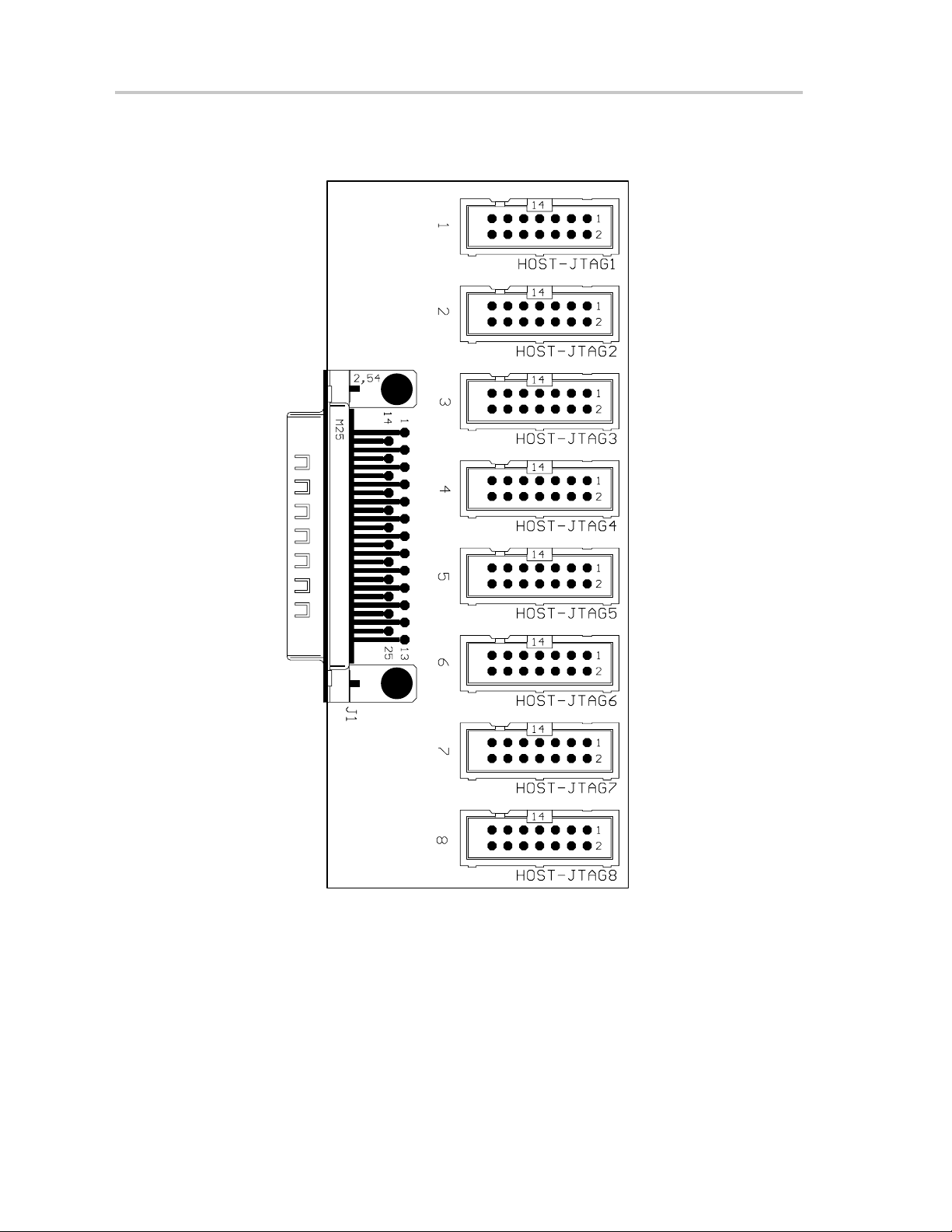
5.4 MSP-GANG430 Target Connector Signals
Figure 5–1, Figure 5–2, and Figure 5–3 show the target connector signals for
the MSP-GANG430. Chapter 5 presents a schematic of the connections
necessary to program multiple target devices.
When an external supply voltage is used for the target systems, it is very
important to disconnect VCC_MSP from the targets to avoid power supply
conflicts that could potential damage the MSP-GANG430 and the targets.
Connect the external supply voltage to MSP_VCC_IN.
It is not possible to use the MSP-GANG430 with targets powered by the
MSP-GANG430 and with targets powered by an external supply
simultaneously.
Hardware
5-3
Page 40

MSP-GANG430 Target Connector Signals
Figure 5–1.25-Pin Sub-D at the MSP-GANG430
TMS
TCK
GND
NC
10
11
12
13
1
14
2
3
4
5
6
7
8
9
VCC_MSP
15
MSP_VCC_IN
16
NC
17
TEST/VPP
18
NC
19
GND
20
GND
21
GND
22
GND
23
GND
24
TDO/TDI8
25
TDO/TDI7
TDO/TDI1
TDI/VPP
VCC_MSP
TDO/TDI1
TDO/TDI2
TDO/TDI3
TDO/TDI4
TDO/TDI5
TDO/TDI6
Figure 5–2.14-Pin Connector at the End of the Interconnect Cable
2 1
VCC_MSP TDO/TDIx
MSP_VCC_IN TDI/VPP
NC TMS
TEST/VPP TCK
NC GND
NC NC
NC NC
14 13
5-4
Page 41

MSP-GANG430 Target Connector Signals
Table 5–2.MSP-GANG430 Target Connector Signal Functions
Signal Name Required Function/Comment
TMS Yes IEE1 149.1 test mode select input
TCK Yes IEE1 149.1 test clock input
TDI/VPP Yes IEE1149.1 test data input multiplexed with fuse blow voltage
input.
TDO/TDI1 to
TDO/TDI8
GND Yes GND is the 0-V terminal
VCC_MSP Yes (if internal supply
MSP_VCC_IN Yes (if external supply
TEST/VPP Yes (depending on
Yes IEE1149.1 test data output multiplexed with Test data input for
use during fuse blow fuse operation.
Software selectable supply voltage VCC to power the targets
voltage is used)
voltage is used)
device)
from the programmer.
External supply voltage sense input, to adapt the internal level
shifter outputs.
Signal used with MSP430 flash devices with TEST/VPP pin.
The output signal levels of the MSP-GANG430 are near GND or VCC_MSP.
- The RST/NMI terminal of the device must be high; otherwise the access
to the device via JTAG fails.
- The programming procedure (handling of the SW) is described in
Chapters 1 and 2 of this manual.
- The connections from the MSP430 terminals must follow EMI rules,
including short trace lengths and use of ground planes.
Table 5–3.MSP-GANG430 Signal Levels
Signal/Pin Signal/Pin Levels
TMS VSS or VCC_MSP
TCK VSS or VCC_MSP
TDI/VPP VSS or VCC_MSP or VPP
TDO/TDI1..8 VSS or VCC_MSP
GND V
VCC_MSP VSS or VCC_MSP
MSP_VCC_IN Input: External VCC of MSP430
TEST/VPP VSS or VCC_MSP or VPP
SS
Hardware
5-5
Page 42

MSP-GANG430 Schematics
Figure 5–3.Typical Connections From Target Connector to Target Device
Connect if target has it’s own
local power source
V
CC
100 nF
Connect to power target from
MSP-GANG430 if not using
a local power source
VCC_MSP
MSP_VCC_IN
TEST/VPP
†
Not present on all devices.
‡
Pins vary by device.
§
Pulldown not required on all devices. Check device data sheet pin description.
2
4
6
8
10
12
14
14 pos. header
(3M p/n 2514–6002)
(Digi-Key p/n MHB14K–ND)
1
3
5
7
9
11
13
TDO/TDIx
TDI/VPP
TMS
TCK
GND
100 kΩ
20 kΩ
§
10 µF
VCC/AVCC/DV
RST/NMI
TDO/TDI
TDI
TMS
TCK
MSP430
PP
†
Test/V
VSS/AVSS/DV
CC
SS
‡
‡
5.5 MSP-GANG430 Schematics
The MSP-GANG430 schematics are presented in Chapter 6.
5-6
Page 43

5.6 MSP-GANG430 Component Locations
Figure 5–4.MSP-GANG430 Component Locations
MSP-GANG430 Component Locations
Hardware
5-7
Page 44
Gang_Exp Target Expansion Board Layout
5.7 Gang_Exp Target Expansion Board Layout
Figure 5–5.Gang_Exp Layout
5-8
Page 45

Chapter 6
Schematics
This chapter presents the schematics of the MSP-GANG430 and the
connections necessary to program multiple target devices.
Schematics
6-1
Page 46

Page 47

Page 48

Page 49

Page 50

Page 51

 Loading...