

Page 1

MSP430x1xx Family
User’s Guide
2000 Mixed Signal Products
SLAU049
Page 2

IMPORTANT NOTICE
T exas Instruments and its subsidiaries (TI) reserve the right to make changes to their products or to discontinue
any product or service without notice, and advise customers to obtain the latest version of relevant information
to verify, before placing orders, that information being relied on is current and complete. All products are sold
subject to the terms and conditions of sale supplied at the time of order acknowledgment, including those
pertaining to warranty, patent infringement, and limitation of liability.
TI warrants performance of its semiconductor products to the specifications applicable at the time of sale in
accordance with TI’s standard warranty. Testing and other quality control techniques are utilized to the extent
TI deems necessary to support this warranty . Specific testing of all parameters of each device is not necessarily
performed, except those mandated by government requirements.
Customers are responsible for their applications using TI components.
In order to minimize risks associated with the customer’s applications, adequate design and operating
safeguards must be provided by the customer to minimize inherent or procedural hazards.
TI assumes no liability for applications assistance or customer product design. TI does not warrant or represent
that any license, either express or implied, is granted under any patent right, copyright, mask work right, or other
intellectual property right of TI covering or relating to any combination, machine, or process in which such
semiconductor products or services might be or are used. TI’s publication of information regarding any third
party’s products or services does not constitute TI’s approval, warranty or endorsement thereof.
Copyright 2000, Texas Instruments Incorporated
Page 3

About This Manual
How to Use This Manual
Preface
Read This First
The MSP430x1xx User’s Guide is intended to assist the development of
MSP430x1xx family products by assembling together and presenting
hardware and software information in a manner that is easy for engineers and
programmers to use.
This manual discusses modules and peripherals of the MSP430x1xx family of
devices. Each discussion presents the module or peripheral in a general
sense. Not all features and functions of all modules or peripherals are present
on all devices. In addition, modules or peripherals may differ in their exact
implementation between device families, or may not be fully implemented on
an individual device or device family. Therefore, a user must always consult
the data sheet of any device of interest to determine what peripherals and
modules are implemented, and exactly how they are implemented on that
particular device.
How to Use This Manual
This document contains the following chapters:
Chapter 1 – Introduction
Chapter 2 – Architectural Overview
Chapter 3 – System Resets, Interrupts, and Operating Modes
Chapter 4 – Memory
Chapter 5 – 16-Bit CPU
Chapter 6 – Hardware Multiplier
Chapter 7 – Basic Clock Module
Chapter 8 – Digital I/O Configuration
Chapter 9 – Watchdog Timer
Chapter 10 – Timer_A
Chapter 11 – Timer_B
Chapter 12 – USART Peripheral Interface, UART Mode
Chapter 13 – USART Peripheral Interface, SPI Mode
Read This First
iii
Page 4

Related Documentation From Texas Instruments
Chapter 14 – Comparator_A
Chapter 15 – ADC12
Appendix A – Peripheral File Map
Appendix B – Instruction Set Description
Appendix C – Flash Memory
Notational Conventions
This document uses the following conventions.
-
Program listings, program examples, and interactive displays are shown
in a special typeface similar to a typewriter’s.
Here is a sample program listing:
0011 0005 0001 .field 1, 2
0012 0005 0003 .field 3, 4
0013 0005 0006 .field 6, 3
0014 0006 .even
Related Documentation From Texas Instruments
FCC Warning
For related documentation see the web site http://www.ti.com/sc/msp430.
This equipment is intended for use in a laboratory test environment only . It generates, uses, and can radiate radio frequency energy and has not been tested
for compliance with the limits of computing devices pursuant to subpart J of
part 15 of FCC rules, which are designed to provide reasonable protection
against radio frequency interference. Operation of this equipment in other environments may cause interference with radio communications, in which case
the user at his own expense will be required to take whatever measures may
be required to correct this interference.
iv
Page 5

Running Title—Attribute Reference
Contents
1 Introduction 1-1. . . . . . . . . . . . . . . . . . . . . . . . . . . . . . . . . . . . . . . . . . . . . . . . . . . . . . . . . . . . . . . . . . . . .
1.1 Features and Capabilities 1-2. . . . . . . . . . . . . . . . . . . . . . . . . . . . . . . . . . . . . . . . . . . . . . . . . . . .
1.2 1 1x Devices 1-3. . . . . . . . . . . . . . . . . . . . . . . . . . . . . . . . . . . . . . . . . . . . . . . . . . . . . . . . . . . . . . . .
1.3 11x1 Devices 1-3. . . . . . . . . . . . . . . . . . . . . . . . . . . . . . . . . . . . . . . . . . . . . . . . . . . . . . . . . . . . . . .
1.4 13x Devices 1-4. . . . . . . . . . . . . . . . . . . . . . . . . . . . . . . . . . . . . . . . . . . . . . . . . . . . . . . . . . . . . . . .
1.5 14x Devices 1-4. . . . . . . . . . . . . . . . . . . . . . . . . . . . . . . . . . . . . . . . . . . . . . . . . . . . . . . . . . . . . . . .
2 Architectural Overview 2-1. . . . . . . . . . . . . . . . . . . . . . . . . . . . . . . . . . . . . . . . . . . . . . . . . . . . . . . . . . .
2.1 Introduction 2-2. . . . . . . . . . . . . . . . . . . . . . . . . . . . . . . . . . . . . . . . . . . . . . . . . . . . . . . . . . . . . . . .
2.2 Central Processing Unit 2-2. . . . . . . . . . . . . . . . . . . . . . . . . . . . . . . . . . . . . . . . . . . . . . . . . . . . .
2.3 Program Memory 2-3. . . . . . . . . . . . . . . . . . . . . . . . . . . . . . . . . . . . . . . . . . . . . . . . . . . . . . . . . . .
2.4 Data Memory 2-3. . . . . . . . . . . . . . . . . . . . . . . . . . . . . . . . . . . . . . . . . . . . . . . . . . . . . . . . . . . . . .
2.5 Operation Control 2-3. . . . . . . . . . . . . . . . . . . . . . . . . . . . . . . . . . . . . . . . . . . . . . . . . . . . . . . . . . .
2.6 Peripherals 2-4. . . . . . . . . . . . . . . . . . . . . . . . . . . . . . . . . . . . . . . . . . . . . . . . . . . . . . . . . . . . . . . .
2.7 Oscillator and Clock Generator 2-4. . . . . . . . . . . . . . . . . . . . . . . . . . . . . . . . . . . . . . . . . . . . . . .
3 System Resets, Interrupts, and Operating Modes 3-1. . . . . . . . . . . . . . . . . . . . . . . . . . . . . . . . . .
3.1 System Reset and Initialization 3-2. . . . . . . . . . . . . . . . . . . . . . . . . . . . . . . . . . . . . . . . . . . . . . .
3.1.1 Introduction 3-2. . . . . . . . . . . . . . . . . . . . . . . . . . . . . . . . . . . . . . . . . . . . . . . . . . . . . . . . .
3.1.2 Device Initialization After System Reset 3-4. . . . . . . . . . . . . . . . . . . . . . . . . . . . . . . .
3.2 Global Interrupt Structure 3-5. . . . . . . . . . . . . . . . . . . . . . . . . . . . . . . . . . . . . . . . . . . . . . . . . . . .
3.3 MSP430 Interrupt-Priority Scheme 3-6. . . . . . . . . . . . . . . . . . . . . . . . . . . . . . . . . . . . . . . . . . . .
3.3.1 Operation of Global Interrupt—Reset/NMI 3-8. . . . . . . . . . . . . . . . . . . . . . . . . . . . . .
3.3.2 Operation of Global Interrupt—Oscillator Fault Control 3-9. . . . . . . . . . . . . . . . . . .
3.4 Interrupt Processing 3-9. . . . . . . . . . . . . . . . . . . . . . . . . . . . . . . . . . . . . . . . . . . . . . . . . . . . . . . .
3.4.1 Interrupt Control Bits in Special-Function Registers (SFRs) 3-11. . . . . . . . . . . . . .
3.4.2 Interrupt Vector Addresses 3-15. . . . . . . . . . . . . . . . . . . . . . . . . . . . . . . . . . . . . . . . . . .
3.5 Operating Modes 3-16. . . . . . . . . . . . . . . . . . . . . . . . . . . . . . . . . . . . . . . . . . . . . . . . . . . . . . . . . .
3.5.1 Low-Power Mode 0 and 1 (LPM0 and LPM1) 3-20. . . . . . . . . . . . . . . . . . . . . . . . . . .
3.5.2 Low-Power Modes 2 and 3 (LPM2 and LPM3) 3-21. . . . . . . . . . . . . . . . . . . . . . . . . .
3.5.3 Low-Power Mode 4 (LPM4) 3-21. . . . . . . . . . . . . . . . . . . . . . . . . . . . . . . . . . . . . . . . . .
3.6 Basic Hints for Low-Power Applications 3-22. . . . . . . . . . . . . . . . . . . . . . . . . . . . . . . . . . . . . . .
4 Memory 4-1. . . . . . . . . . . . . . . . . . . . . . . . . . . . . . . . . . . . . . . . . . . . . . . . . . . . . . . . . . . . . . . . . . . . . . . . .
4.1 Introduction 4-2. . . . . . . . . . . . . . . . . . . . . . . . . . . . . . . . . . . . . . . . . . . . . . . . . . . . . . . . . . . . . . . .
4.2 Data in the Memory 4-3. . . . . . . . . . . . . . . . . . . . . . . . . . . . . . . . . . . . . . . . . . . . . . . . . . . . . . . . .
4.3 Internal ROM Organization 4-4. . . . . . . . . . . . . . . . . . . . . . . . . . . . . . . . . . . . . . . . . . . . . . . . . . .
4.3.1 Processing of ROM Tables 4-4. . . . . . . . . . . . . . . . . . . . . . . . . . . . . . . . . . . . . . . . . . . .
4.3.2 Computed Branches and Calls 4-5. . . . . . . . . . . . . . . . . . . . . . . . . . . . . . . . . . . . . . . .
Chapter Title—Attribute Reference
v
Page 6

Contents
4.4 RAM and Peripheral Organization 4-6. . . . . . . . . . . . . . . . . . . . . . . . . . . . . . . . . . . . . . . . . . . .
4.4.1 Random Access Memory 4-6. . . . . . . . . . . . . . . . . . . . . . . . . . . . . . . . . . . . . . . . . . . . .
4.4.2 Peripheral Modules—Address Allocation 4-8. . . . . . . . . . . . . . . . . . . . . . . . . . . . . . .
4.4.3 Peripheral Modules—Special Function Registers (SFRs) 4-10. . . . . . . . . . . . . . . .
5 16-Bit CPU 5-1. . . . . . . . . . . . . . . . . . . . . . . . . . . . . . . . . . . . . . . . . . . . . . . . . . . . . . . . . . . . . . . . . . . . . .
5.1 CPU Registers 5-2. . . . . . . . . . . . . . . . . . . . . . . . . . . . . . . . . . . . . . . . . . . . . . . . . . . . . . . . . . . . .
5.1.1 The Program Counter (PC) 5-2. . . . . . . . . . . . . . . . . . . . . . . . . . . . . . . . . . . . . . . . . . .
5.1.2 The System Stack Pointer (SP) 5-2. . . . . . . . . . . . . . . . . . . . . . . . . . . . . . . . . . . . . . . .
5.1.3 The Status Register (SR) 5-4. . . . . . . . . . . . . . . . . . . . . . . . . . . . . . . . . . . . . . . . . . . . .
5.1.4 The Constant Generator Registers CG1 and CG2 5-5. . . . . . . . . . . . . . . . . . . . . . .
5.2 Addressing Modes 5-7. . . . . . . . . . . . . . . . . . . . . . . . . . . . . . . . . . . . . . . . . . . . . . . . . . . . . . . . . .
5.2.1 Register Mode 5-8. . . . . . . . . . . . . . . . . . . . . . . . . . . . . . . . . . . . . . . . . . . . . . . . . . . . . .
5.2.2 Indexed Mode 5-9. . . . . . . . . . . . . . . . . . . . . . . . . . . . . . . . . . . . . . . . . . . . . . . . . . . . . . .
5.2.3 Symbolic Mode 5-10. . . . . . . . . . . . . . . . . . . . . . . . . . . . . . . . . . . . . . . . . . . . . . . . . . . . .
5.2.4 Absolute Mode 5-11. . . . . . . . . . . . . . . . . . . . . . . . . . . . . . . . . . . . . . . . . . . . . . . . . . . . .
5.2.5 Indirect Mode 5-12. . . . . . . . . . . . . . . . . . . . . . . . . . . . . . . . . . . . . . . . . . . . . . . . . . . . . .
5.2.6 Indirect Autoincrement Mode 5-13. . . . . . . . . . . . . . . . . . . . . . . . . . . . . . . . . . . . . . . . .
5.2.7 Immediate Mode 5-14. . . . . . . . . . . . . . . . . . . . . . . . . . . . . . . . . . . . . . . . . . . . . . . . . . .
5.2.8 Clock Cycles, Length of Instruction 5-15. . . . . . . . . . . . . . . . . . . . . . . . . . . . . . . . . . .
5.3 Instruction Set Overview 5-17. . . . . . . . . . . . . . . . . . . . . . . . . . . . . . . . . . . . . . . . . . . . . . . . . . . .
5.3.1 Double-Operand Instructions 5-18. . . . . . . . . . . . . . . . . . . . . . . . . . . . . . . . . . . . . . . . .
5.3.2 Single-Operand Instructions 5-19. . . . . . . . . . . . . . . . . . . . . . . . . . . . . . . . . . . . . . . . .
5.3.3 Conditional Jumps 5-20. . . . . . . . . . . . . . . . . . . . . . . . . . . . . . . . . . . . . . . . . . . . . . . . . .
5.3.4 Short Form of Emulated Instructions 5-21. . . . . . . . . . . . . . . . . . . . . . . . . . . . . . . . . .
5.3.5 Miscellaneous 5-22. . . . . . . . . . . . . . . . . . . . . . . . . . . . . . . . . . . . . . . . . . . . . . . . . . . . . .
5.4 Instruction Map 5-23. . . . . . . . . . . . . . . . . . . . . . . . . . . . . . . . . . . . . . . . . . . . . . . . . . . . . . . . . . . .
6 Hardware Multiplier 6-1. . . . . . . . . . . . . . . . . . . . . . . . . . . . . . . . . . . . . . . . . . . . . . . . . . . . . . . . . . . . . .
6.1 Hardware Multiplier Module Support 6-2. . . . . . . . . . . . . . . . . . . . . . . . . . . . . . . . . . . . . . . . . .
6.2 Hardware Multiplier Operation 6-3. . . . . . . . . . . . . . . . . . . . . . . . . . . . . . . . . . . . . . . . . . . . . . . .
6.2.1 Multiply Unsigned, 16×16 bit, 16×8 bit, 8× 16 bit, 8×8 bit 6-5. . . . . . . . . . . . . . . .
6.2.2 Multiply Signed, 16×16 bit, 16×8 bit, 8×16 bit, 8×8 bit 6-6. . . . . . . . . . . . . . . . . . . .
6.2.3 Multiply Unsigned and Accumulate, 16x16bit, 16x8bit, 8x16bit, 8x8bit 6-7. . . . . .
6.2.4 Multiply Signed and Accumulate, 16x16bit, 16x8bit, 8x16bit, 8x8bit 6-8. . . . . . . .
6.3 Hardware Multiplier Registers 6-9. . . . . . . . . . . . . . . . . . . . . . . . . . . . . . . . . . . . . . . . . . . . . . . .
6.4 Hardware Multiplier Special Function Bits 6-10. . . . . . . . . . . . . . . . . . . . . . . . . . . . . . . . . . . . .
6.5 Hardware Multiplier Software Restrictions 6-10. . . . . . . . . . . . . . . . . . . . . . . . . . . . . . . . . . . . .
6.5.1 Hardware Multiplier Software Restrictions—Address Mode 6-10. . . . . . . . . . . . . . .
6.5.2 Hardware Multiplier Software Restrictions—Interrupt Routines 6-11. . . . . . . . . . . .
6.5.3 Hardware Multiplier Software Restrictions—MACS 6-12. . . . . . . . . . . . . . . . . . . . . .
7 Basic Clock Module 7-1. . . . . . . . . . . . . . . . . . . . . . . . . . . . . . . . . . . . . . . . . . . . . . . . . . . . . . . . . . . . .
7.1 Basic Clock Module 7-2. . . . . . . . . . . . . . . . . . . . . . . . . . . . . . . . . . . . . . . . . . . . . . . . . . . . . . . . .
7.2 LFXT1 and XT2 Oscillators 7-4. . . . . . . . . . . . . . . . . . . . . . . . . . . . . . . . . . . . . . . . . . . . . . . . . .
7.2.1 LFXT1 Oscillator 7-4. . . . . . . . . . . . . . . . . . . . . . . . . . . . . . . . . . . . . . . . . . . . . . . . . . . .
7.2.2 XT2 Oscillator 7-5. . . . . . . . . . . . . . . . . . . . . . . . . . . . . . . . . . . . . . . . . . . . . . . . . . . . . . .
7.2.3 Oscillator Fault Detection 7-6. . . . . . . . . . . . . . . . . . . . . . . . . . . . . . . . . . . . . . . . . . . . .
7.2.4 Select DCO Oscillator for MCLK on XT Oscillator Fault 7-8. . . . . . . . . . . . . . . . . . .
7.3 Digitally-Controlled Oscillator (DCO) 7-10. . . . . . . . . . . . . . . . . . . . . . . . . . . . . . . . . . . . . . . . .
7.3.1 Operation of the DCO Modulator 7-12. . . . . . . . . . . . . . . . . . . . . . . . . . . . . . . . . . . . .
vi
Page 7

Contents
7.4 Basic Clock Module Operating Modes 7-14. . . . . . . . . . . . . . . . . . . . . . . . . . . . . . . . . . . . . . . .
7.4.1 Starting From Power Up Clear (PUC) 7-14. . . . . . . . . . . . . . . . . . . . . . . . . . . . . . . . .
7.4.2 Adjusting the Basic Clock 7-14. . . . . . . . . . . . . . . . . . . . . . . . . . . . . . . . . . . . . . . . . . . .
7.4.3 Basic Clock Features for Low-Power Applications 7-15. . . . . . . . . . . . . . . . . . . . . .
7.4.4 Selecting a Crystal Clock for MCLK 7-15. . . . . . . . . . . . . . . . . . . . . . . . . . . . . . . . . . .
7.4.5 Synchronization of Clock Signals 7-17. . . . . . . . . . . . . . . . . . . . . . . . . . . . . . . . . . . . .
7.5 Basic Clock Module Control Registers 7-18. . . . . . . . . . . . . . . . . . . . . . . . . . . . . . . . . . . . . . . .
7.5.1 Digitally-Controlled Oscillator (DCO) Clock-Frequency Control 7-18. . . . . . . . . . .
7.5.2 Oscillator and Clock Control Register 7-18. . . . . . . . . . . . . . . . . . . . . . . . . . . . . . . . .
7.5.3 Special-Function Register Bits 7-20. . . . . . . . . . . . . . . . . . . . . . . . . . . . . . . . . . . . . . .
8 Digital I/O Configuration 8-1. . . . . . . . . . . . . . . . . . . . . . . . . . . . . . . . . . . . . . . . . . . . . . . . . . . . . . . . .
8.1 Introduction 8-2. . . . . . . . . . . . . . . . . . . . . . . . . . . . . . . . . . . . . . . . . . . . . . . . . . . . . . . . . . . . . . . .
8.2 Ports P1, P2 8-3. . . . . . . . . . . . . . . . . . . . . . . . . . . . . . . . . . . . . . . . . . . . . . . . . . . . . . . . . . . . . . .
8.2.1 Port P1, Port P2 Control Registers 8-4. . . . . . . . . . . . . . . . . . . . . . . . . . . . . . . . . . . . .
8.2.2 Port P1, Port P2 Schematic 8-7. . . . . . . . . . . . . . . . . . . . . . . . . . . . . . . . . . . . . . . . . . .
8.2.3 Port P1, P2 Interrupt Control Functions 8-8. . . . . . . . . . . . . . . . . . . . . . . . . . . . . . . . .
8.3 Ports P3, P4, P5, P6 8-9. . . . . . . . . . . . . . . . . . . . . . . . . . . . . . . . . . . . . . . . . . . . . . . . . . . . . . . .
8.3.1 Port P3–P6 Control Registers 8-9. . . . . . . . . . . . . . . . . . . . . . . . . . . . . . . . . . . . . . . . .
8.3.2 Port P3–P6 Schematic 8-1 1. . . . . . . . . . . . . . . . . . . . . . . . . . . . . . . . . . . . . . . . . . . . . .
9 Watchdog Timer 9-1. . . . . . . . . . . . . . . . . . . . . . . . . . . . . . . . . . . . . . . . . . . . . . . . . . . . . . . . . . . . . . . . .
9.1 The Watchdog Timer 9-2. . . . . . . . . . . . . . . . . . . . . . . . . . . . . . . . . . . . . . . . . . . . . . . . . . . . . . . .
9.1.1 Watchdog Timer Register 9-3. . . . . . . . . . . . . . . . . . . . . . . . . . . . . . . . . . . . . . . . . . . . .
9.1.2 Watchdog Timer Interrupt Control Functions 9-5. . . . . . . . . . . . . . . . . . . . . . . . . . . .
9.1.3 Watchdog Timer Operation 9-5. . . . . . . . . . . . . . . . . . . . . . . . . . . . . . . . . . . . . . . . . . .
10 Timer_A 10-1. . . . . . . . . . . . . . . . . . . . . . . . . . . . . . . . . . . . . . . . . . . . . . . . . . . . . . . . . . . . . . . . . . . . . . .
10.1 Introduction 10-2. . . . . . . . . . . . . . . . . . . . . . . . . . . . . . . . . . . . . . . . . . . . . . . . . . . . . . . . . . . . . . .
10.2 Timer_A Operation 10-4. . . . . . . . . . . . . . . . . . . . . . . . . . . . . . . . . . . . . . . . . . . . . . . . . . . . . . . . .
10.2.1 Timer Mode Control 10-4. . . . . . . . . . . . . . . . . . . . . . . . . . . . . . . . . . . . . . . . . . . . . . . . .
10.2.2 Clock Source Select and Divider 10-5. . . . . . . . . . . . . . . . . . . . . . . . . . . . . . . . . . . . . .
10.2.3 Starting the Timer 10-6. . . . . . . . . . . . . . . . . . . . . . . . . . . . . . . . . . . . . . . . . . . . . . . . . .
10.3 Timer Modes 10-7. . . . . . . . . . . . . . . . . . . . . . . . . . . . . . . . . . . . . . . . . . . . . . . . . . . . . . . . . . . . . .
10.3.1 Timer—Stop Mode 10-7. . . . . . . . . . . . . . . . . . . . . . . . . . . . . . . . . . . . . . . . . . . . . . . . .
10.3.2 Timer—Up Mode 10-7. . . . . . . . . . . . . . . . . . . . . . . . . . . . . . . . . . . . . . . . . . . . . . . . . . .
10.3.3 Timer—Continuous Mode 10-9. . . . . . . . . . . . . . . . . . . . . . . . . . . . . . . . . . . . . . . . . . .
10.3.4 Timer—Up/Down Mode 10-10. . . . . . . . . . . . . . . . . . . . . . . . . . . . . . . . . . . . . . . . . . . .
10.4 Capture/Compare Blocks 10-13. . . . . . . . . . . . . . . . . . . . . . . . . . . . . . . . . . . . . . . . . . . . . . . . . .
10.4.1 Capture/Compare Block—Capture Mode 10-14. . . . . . . . . . . . . . . . . . . . . . . . . . . . .
10.4.2 Capture/Compare Block—Compare Mode 10-18. . . . . . . . . . . . . . . . . . . . . . . . . . . .
10.5 The Output Unit 10-19. . . . . . . . . . . . . . . . . . . . . . . . . . . . . . . . . . . . . . . . . . . . . . . . . . . . . . . . . .
10.5.1 Output Unit—Output Modes 10-20. . . . . . . . . . . . . . . . . . . . . . . . . . . . . . . . . . . . . . . . .
10.5.2 Output Control Block 10-21. . . . . . . . . . . . . . . . . . . . . . . . . . . . . . . . . . . . . . . . . . . . . . .
10.5.3 Output Examples 10-22. . . . . . . . . . . . . . . . . . . . . . . . . . . . . . . . . . . . . . . . . . . . . . . . . .
10.6 Timer_A Registers 10-24. . . . . . . . . . . . . . . . . . . . . . . . . . . . . . . . . . . . . . . . . . . . . . . . . . . . . . . .
10.6.1 Timer_A Control Register TACTL 10-25. . . . . . . . . . . . . . . . . . . . . . . . . . . . . . . . . . . .
10.6.2 Timer_A Register TAR 10-26. . . . . . . . . . . . . . . . . . . . . . . . . . . . . . . . . . . . . . . . . . . . .
10.6.3 Capture/Compare Control Register CCTLx 10-27. . . . . . . . . . . . . . . . . . . . . . . . . . .
10.6.4 Timer_A Interrupt Vector Register 10-29. . . . . . . . . . . . . . . . . . . . . . . . . . . . . . . . . . .
10.7 Timer_A UART 10-33. . . . . . . . . . . . . . . . . . . . . . . . . . . . . . . . . . . . . . . . . . . . . . . . . . . . . . . . . . .
Contents
vii
Page 8

Contents
11 Timer_B 11-1. . . . . . . . . . . . . . . . . . . . . . . . . . . . . . . . . . . . . . . . . . . . . . . . . . . . . . . . . . . . . . . . . . . . . . .
1 1.1 Introduction 11-2. . . . . . . . . . . . . . . . . . . . . . . . . . . . . . . . . . . . . . . . . . . . . . . . . . . . . . . . . . . . . . .
11.1.1 Similarities and Differences From Timer_A 11-2. . . . . . . . . . . . . . . . . . . . . . . . . . . . .
11.2 Timer_B Operation 11-5. . . . . . . . . . . . . . . . . . . . . . . . . . . . . . . . . . . . . . . . . . . . . . . . . . . . . . . . .
11.2.1 Timer Length 11-5. . . . . . . . . . . . . . . . . . . . . . . . . . . . . . . . . . . . . . . . . . . . . . . . . . . . . .
11.2.2 Timer Mode Control 11-5. . . . . . . . . . . . . . . . . . . . . . . . . . . . . . . . . . . . . . . . . . . . . . . . .
11.2.3 Clock Source Select and Divider 11-6. . . . . . . . . . . . . . . . . . . . . . . . . . . . . . . . . . . . . .
11.2.4 Starting the Timer 11-7. . . . . . . . . . . . . . . . . . . . . . . . . . . . . . . . . . . . . . . . . . . . . . . . . .
11.3 Timer Modes 11-8. . . . . . . . . . . . . . . . . . . . . . . . . . . . . . . . . . . . . . . . . . . . . . . . . . . . . . . . . . . . . .
11.3.1 Timer—Stop Mode 11-8. . . . . . . . . . . . . . . . . . . . . . . . . . . . . . . . . . . . . . . . . . . . . . . . .
11.3.2 Timer—Up Mode 11-8. . . . . . . . . . . . . . . . . . . . . . . . . . . . . . . . . . . . . . . . . . . . . . . . . . .
11.3.3 Timer—Continuous Mode 11-10. . . . . . . . . . . . . . . . . . . . . . . . . . . . . . . . . . . . . . . . . .
11.3.4 Timer—Up/Down Mode 11-12. . . . . . . . . . . . . . . . . . . . . . . . . . . . . . . . . . . . . . . . . . . .
1 1.4 Capture/Compare Blocks 11-15. . . . . . . . . . . . . . . . . . . . . . . . . . . . . . . . . . . . . . . . . . . . . . . . . .
11.4.1 Capture/Compare Block—Capture Mode 11-16. . . . . . . . . . . . . . . . . . . . . . . . . . . . .
11.4.2 Capture/Compare Block—Compare Mode 11-19. . . . . . . . . . . . . . . . . . . . . . . . . . . .
11.5 The Output Unit 11-23. . . . . . . . . . . . . . . . . . . . . . . . . . . . . . . . . . . . . . . . . . . . . . . . . . . . . . . . . .
11.5.2 Output Control Block 11-25. . . . . . . . . . . . . . . . . . . . . . . . . . . . . . . . . . . . . . . . . . . . . . .
1 1.5.3 Output Examples 11-26. . . . . . . . . . . . . . . . . . . . . . . . . . . . . . . . . . . . . . . . . . . . . . . . . .
11.6 Timer_B Registers 11-29. . . . . . . . . . . . . . . . . . . . . . . . . . . . . . . . . . . . . . . . . . . . . . . . . . . . . . . .
11.6.1 Timer_B Control Register TBCTL 11-29. . . . . . . . . . . . . . . . . . . . . . . . . . . . . . . . . . . .
11.6.2 Timer_B Register TBR 11-32. . . . . . . . . . . . . . . . . . . . . . . . . . . . . . . . . . . . . . . . . . . . .
11.6.3 Capture/Compare Control Register CCTLx 11-32. . . . . . . . . . . . . . . . . . . . . . . . . . .
11.6.4 Timer_B Interrupt Vector Register 11-35. . . . . . . . . . . . . . . . . . . . . . . . . . . . . . . . . . .
12 USART Peripheral Interface, UART Mode 12-1. . . . . . . . . . . . . . . . . . . . . . . . . . . . . . . . . . . . . . . . .
12.1 USART Peripheral Interface 12-2. . . . . . . . . . . . . . . . . . . . . . . . . . . . . . . . . . . . . . . . . . . . . . . . .
12.2 USART Peripheral Interface, UART Mode 12-3. . . . . . . . . . . . . . . . . . . . . . . . . . . . . . . . . . . . .
12.2.1 UART Serial Asynchronous Communication Features 12-3. . . . . . . . . . . . . . . . . . .
12.3 Asynchronous Operation 12-4. . . . . . . . . . . . . . . . . . . . . . . . . . . . . . . . . . . . . . . . . . . . . . . . . . .
12.3.1 Asynchronous Frame Format 12-4. . . . . . . . . . . . . . . . . . . . . . . . . . . . . . . . . . . . . . . .
12.3.2 Baud Rate Generation in Asynchronous Communication Format 12-5. . . . . . . . . .
12.3.3 Asynchronous Communication Formats 12-7. . . . . . . . . . . . . . . . . . . . . . . . . . . . . . .
12.3.4 Idle-Line Multiprocessor Format 12-7. . . . . . . . . . . . . . . . . . . . . . . . . . . . . . . . . . . . . .
12.3.5 Address-Bit Multiprocessor Format 12-9. . . . . . . . . . . . . . . . . . . . . . . . . . . . . . . . . . .
12.4 Interrupt and Enable Functions 12-11. . . . . . . . . . . . . . . . . . . . . . . . . . . . . . . . . . . . . . . . . . . . .
12.4.1 USART Receive Enable Bit 12-11. . . . . . . . . . . . . . . . . . . . . . . . . . . . . . . . . . . . . . . . .
12.4.2 USART Transmit Enable Bit 12-12. . . . . . . . . . . . . . . . . . . . . . . . . . . . . . . . . . . . . . . . .
12.4.3 USART Receive Interrupt Operation 12-13. . . . . . . . . . . . . . . . . . . . . . . . . . . . . . . . .
12.4.4 USART Transmit Interrupt Operation 12-14. . . . . . . . . . . . . . . . . . . . . . . . . . . . . . . . .
12.5 Control and Status Registers 12-15. . . . . . . . . . . . . . . . . . . . . . . . . . . . . . . . . . . . . . . . . . . . . . .
12.5.1 USART Control Register UCTL 12-16. . . . . . . . . . . . . . . . . . . . . . . . . . . . . . . . . . . . . .
12.5.2 Transmit Control Register UTCTL 12-17. . . . . . . . . . . . . . . . . . . . . . . . . . . . . . . . . . .
12.5.3 Receiver Control Register URCTL 12-18. . . . . . . . . . . . . . . . . . . . . . . . . . . . . . . . . . .
12.5.4 Baud Rate Select and Modulation Control Registers 12-20. . . . . . . . . . . . . . . . . . .
12.5.5 Receive-Data Buffer URXBUF 12-21. . . . . . . . . . . . . . . . . . . . . . . . . . . . . . . . . . . . . .
12.5.6 Transmit Data Buffer UTXBUF 12-21. . . . . . . . . . . . . . . . . . . . . . . . . . . . . . . . . . . . . .
12.6 Utilizing Features of Low-Power Modes 12-22. . . . . . . . . . . . . . . . . . . . . . . . . . . . . . . . . . . . . .
12.6.1 Receive-Start Operation From UART Frame 12-22. . . . . . . . . . . . . . . . . . . . . . . . . .
12.6.2 Maximum Utilization of Clock Frequency vs Baud Rate UART Mode 12-24. . . . .
12.6.3 Support of Multiprocessor Modes for Reduced Use of
MSP430 Resources 12-25. . . . . . . . . . . . . . . . . . . . . . . . . . . . . . . . . . . . . . . . . . . . . . .
viii
Page 9

Contents
12.7 Baud Rate Considerations 12-25. . . . . . . . . . . . . . . . . . . . . . . . . . . . . . . . . . . . . . . . . . . . . . . . .
12.7.1 Bit Timing in Transmit Operation 12-25. . . . . . . . . . . . . . . . . . . . . . . . . . . . . . . . . . . . .
12.7.2 Typical Baud Rates and Errors 12-27. . . . . . . . . . . . . . . . . . . . . . . . . . . . . . . . . . . . . .
12.7.3 Synchronization Error 12-28. . . . . . . . . . . . . . . . . . . . . . . . . . . . . . . . . . . . . . . . . . . . . .
13 USART Peripheral Interface, SPI Mode 13-1. . . . . . . . . . . . . . . . . . . . . . . . . . . . . . . . . . . . . . . . . . .
13.1 USART Peripheral Interface 13-2. . . . . . . . . . . . . . . . . . . . . . . . . . . . . . . . . . . . . . . . . . . . . . . . .
13.2 USART Peripheral Interface, SPI Mode 13-3. . . . . . . . . . . . . . . . . . . . . . . . . . . . . . . . . . . . . . .
13.2.1 SPI Mode Features 13-3. . . . . . . . . . . . . . . . . . . . . . . . . . . . . . . . . . . . . . . . . . . . . . . . .
13.3 Synchronous Operation 13-4. . . . . . . . . . . . . . . . . . . . . . . . . . . . . . . . . . . . . . . . . . . . . . . . . . . .
13.3.1 Master SPI Mode 13-7. . . . . . . . . . . . . . . . . . . . . . . . . . . . . . . . . . . . . . . . . . . . . . . . . . .
13.3.2 Slave SPI Mode 13-8. . . . . . . . . . . . . . . . . . . . . . . . . . . . . . . . . . . . . . . . . . . . . . . . . . . .
13.4 Interrupt and Control Functions 13-9. . . . . . . . . . . . . . . . . . . . . . . . . . . . . . . . . . . . . . . . . . . . . .
13.4.1 USART Receive/T ransmit Enable Bit, Receive Operation 13-9. . . . . . . . . . . . . . . .
13.4.2 USART Receive/T ransmit Enable Bit, Transmit Operation 13-11. . . . . . . . . . . . . . .
13.4.3 USART Receive-Interrupt Operation 13-13. . . . . . . . . . . . . . . . . . . . . . . . . . . . . . . . .
13.4.4 Transmit-Interrupt Operation 13-14. . . . . . . . . . . . . . . . . . . . . . . . . . . . . . . . . . . . . . . .
13.5 Control and Status Registers 13-15. . . . . . . . . . . . . . . . . . . . . . . . . . . . . . . . . . . . . . . . . . . . . . .
13.5.1 USART Control Register 13-16. . . . . . . . . . . . . . . . . . . . . . . . . . . . . . . . . . . . . . . . . . .
13.5.2 Transmit Control Register UTCTL 13-16. . . . . . . . . . . . . . . . . . . . . . . . . . . . . . . . . . .
13.5.3 Receive Control Register URCTL 13-18. . . . . . . . . . . . . . . . . . . . . . . . . . . . . . . . . . . .
13.5.4 Baud-Rate Select and Modulation Control Registers 13-19. . . . . . . . . . . . . . . . . . .
13.5.5 Receive Data Buffer URXBUF 13-19. . . . . . . . . . . . . . . . . . . . . . . . . . . . . . . . . . . . . . .
13.5.6 Transmit Data Buffer UTXBUF 13-20. . . . . . . . . . . . . . . . . . . . . . . . . . . . . . . . . . . . . .
14 Comparator_A 14-1. . . . . . . . . . . . . . . . . . . . . . . . . . . . . . . . . . . . . . . . . . . . . . . . . . . . . . . . . . . . . . . . . .
14.1 Comparator_A Overview 14-2. . . . . . . . . . . . . . . . . . . . . . . . . . . . . . . . . . . . . . . . . . . . . . . . . . .
14.2 Comparator_A Description 14-3. . . . . . . . . . . . . . . . . . . . . . . . . . . . . . . . . . . . . . . . . . . . . . . . . .
14.2.1 Input Analog Switches 14-3. . . . . . . . . . . . . . . . . . . . . . . . . . . . . . . . . . . . . . . . . . . . . .
14.2.2 Input Multiplexer 14-3. . . . . . . . . . . . . . . . . . . . . . . . . . . . . . . . . . . . . . . . . . . . . . . . . . . .
14.2.3 The Comparator 14-3. . . . . . . . . . . . . . . . . . . . . . . . . . . . . . . . . . . . . . . . . . . . . . . . . . . .
14.2.4 The Output Filter 14-3. . . . . . . . . . . . . . . . . . . . . . . . . . . . . . . . . . . . . . . . . . . . . . . . . . .
14.2.5 The Voltage Reference Generator 14-4. . . . . . . . . . . . . . . . . . . . . . . . . . . . . . . . . . . .
14.2.6 Comparator_A Interrupt Circuitry 14-5. . . . . . . . . . . . . . . . . . . . . . . . . . . . . . . . . . . . .
14.3 Comparator_A Control Registers 14-6. . . . . . . . . . . . . . . . . . . . . . . . . . . . . . . . . . . . . . . . . . . .
14.3.1 Comparator_A, Control Register CACTL1 14-6. . . . . . . . . . . . . . . . . . . . . . . . . . . . .
14.3.2 Comparator_A, Control Register CACTL2 14-7. . . . . . . . . . . . . . . . . . . . . . . . . . . . .
14.3.3 Comparator_A, Port Disable Register CAPD 14-7. . . . . . . . . . . . . . . . . . . . . . . . . . .
14.4 Comparator_A in Applications 14-9. . . . . . . . . . . . . . . . . . . . . . . . . . . . . . . . . . . . . . . . . . . . . . .
14.4.1 Analog Signals at Digital Inputs 14-9. . . . . . . . . . . . . . . . . . . . . . . . . . . . . . . . . . . . . . .
14.4.2 Comparator_A Used to Measure Resistive Elements 14-11. . . . . . . . . . . . . . . . . . .
14.4.3 Measuring Two Independent Resistive Element Systems 14-13. . . . . . . . . . . . . . .
14.4.4 Comparator_A Used to Detect a Current or Voltage Level 14-16. . . . . . . . . . . . . . .
14.4.5 Comparator_A Used to Measure a Current or Voltage Level 14-17. . . . . . . . . . . . .
14.4.6 Measuring the Offset Voltage of Comparator_A 14-20. . . . . . . . . . . . . . . . . . . . . . . .
14.4.7 Compensating for the Offset Voltage of Comparator_A 14-22. . . . . . . . . . . . . . . . .
14.4.8 Adding Hysteresis to Comparator_A 14-22. . . . . . . . . . . . . . . . . . . . . . . . . . . . . . . . .
15 ADC12 15-1. . . . . . . . . . . . . . . . . . . . . . . . . . . . . . . . . . . . . . . . . . . . . . . . . . . . . . . . . . . . . . . . . . . . . . . . .
15.1 Introduction 15-2. . . . . . . . . . . . . . . . . . . . . . . . . . . . . . . . . . . . . . . . . . . . . . . . . . . . . . . . . . . . . . .
15.2 ADC12 Description and Operation 15-4. . . . . . . . . . . . . . . . . . . . . . . . . . . . . . . . . . . . . . . . . . .
Contents
ix
Page 10

Contents
15.2.1 ADC Core 15-4. . . . . . . . . . . . . . . . . . . . . . . . . . . . . . . . . . . . . . . . . . . . . . . . . . . . . . . . .
15.2.2 Reference 15-5. . . . . . . . . . . . . . . . . . . . . . . . . . . . . . . . . . . . . . . . . . . . . . . . . . . . . . . . .
15.3 Analog Inputs and Multiplexer 15-6. . . . . . . . . . . . . . . . . . . . . . . . . . . . . . . . . . . . . . . . . . . . . . .
15.3.1 Analog Multiplexer 15-6. . . . . . . . . . . . . . . . . . . . . . . . . . . . . . . . . . . . . . . . . . . . . . . . . .
15.3.2 Input Signal Considerations 15-7. . . . . . . . . . . . . . . . . . . . . . . . . . . . . . . . . . . . . . . . . .
15.3.3 Using the Temperature Diode 15-7. . . . . . . . . . . . . . . . . . . . . . . . . . . . . . . . . . . . . . . .
15.4 Conversion Memory 15-8. . . . . . . . . . . . . . . . . . . . . . . . . . . . . . . . . . . . . . . . . . . . . . . . . . . . . . .
15.5 Conversion Modes 15-9. . . . . . . . . . . . . . . . . . . . . . . . . . . . . . . . . . . . . . . . . . . . . . . . . . . . . . . . .
15.5.1 Single-Channel, Single-Conversion Mode 15-9. . . . . . . . . . . . . . . . . . . . . . . . . . . . .
15.5.2 Sequence-of-Channels Mode 15-12. . . . . . . . . . . . . . . . . . . . . . . . . . . . . . . . . . . . . . .
15.5.3 Repeat-Single-Channel Mode 15-16. . . . . . . . . . . . . . . . . . . . . . . . . . . . . . . . . . . . . . .
15.5.4 Repeat-Sequence-of-Channels Mode 15-17. . . . . . . . . . . . . . . . . . . . . . . . . . . . . . . .
15.5.5 Switching Between Conversion Modes 15-19. . . . . . . . . . . . . . . . . . . . . . . . . . . . . . .
15.5.6 Power Down 15-20. . . . . . . . . . . . . . . . . . . . . . . . . . . . . . . . . . . . . . . . . . . . . . . . . . . . . .
15.6 Conversion Clock and Conversion Speed 15-21. . . . . . . . . . . . . . . . . . . . . . . . . . . . . . . . . . . .
15.7 Sampling 15-22. . . . . . . . . . . . . . . . . . . . . . . . . . . . . . . . . . . . . . . . . . . . . . . . . . . . . . . . . . . . . . . .
15.7.1 Sampling Operation 15-22. . . . . . . . . . . . . . . . . . . . . . . . . . . . . . . . . . . . . . . . . . . . . . . .
15.7.2 Sample Signal Input Selection 15-23. . . . . . . . . . . . . . . . . . . . . . . . . . . . . . . . . . . . . . .
15.7.3 Sampling Modes 15-24. . . . . . . . . . . . . . . . . . . . . . . . . . . . . . . . . . . . . . . . . . . . . . . . . .
15.7.4 Using the MSC Bit 15-27. . . . . . . . . . . . . . . . . . . . . . . . . . . . . . . . . . . . . . . . . . . . . . . . .
15.7.5 Sample Timing Considerations 15-29. . . . . . . . . . . . . . . . . . . . . . . . . . . . . . . . . . . . . .
15.8 ADC12 Control Registers 15-30. . . . . . . . . . . . . . . . . . . . . . . . . . . . . . . . . . . . . . . . . . . . . . . . . .
15.8.1 Control Registers ADC12CTL0 and ADC12CTL1 15-31. . . . . . . . . . . . . . . . . . . . . .
15.8.2 Conversion-Memory Registers ADC12MEMx 15-35. . . . . . . . . . . . . . . . . . . . . . . . .
15.8.3 Control Registers ADC12MCTLx 15-35. . . . . . . . . . . . . . . . . . . . . . . . . . . . . . . . . . . .
15.8.4 ADC12 Interrupt Flags ADC12IFG.x and Interrupt-Enable Registers
ADC12IEN.x 15-37. . . . . . . . . . . . . . . . . . . . . . . . . . . . . . . . . . . . . . . . . . . . . . . . . . . . . .
15.8.5 ADC12 Interrupt Vector Register ADC12IV 15-37. . . . . . . . . . . . . . . . . . . . . . . . . . . .
15.9 A/D Grounding and Noise Considerations 15-41. . . . . . . . . . . . . . . . . . . . . . . . . . . . . . . . . . . .
A Peripheral File Map A-1. . . . . . . . . . . . . . . . . . . . . . . . . . . . . . . . . . . . . . . . . . . . . . . . . . . . . . . . . . . . . .
A.1 Overview A-2. . . . . . . . . . . . . . . . . . . . . . . . . . . . . . . . . . . . . . . . . . . . . . . . . . . . . . . . . . . . . . . . . .
A.2 Special Function Register of MSP430x1xx Family, Byte Access A-3. . . . . . . . . . . . . . . . . . .
A.3 Digital I/O, Byte Access A-3. . . . . . . . . . . . . . . . . . . . . . . . . . . . . . . . . . . . . . . . . . . . . . . . . . . . . .
A.4 Basic Clock Registers, Byte Access A-5. . . . . . . . . . . . . . . . . . . . . . . . . . . . . . . . . . . . . . . . . .
A.5 EPROM Control Register Byte Access A-5. . . . . . . . . . . . . . . . . . . . . . . . . . . . . . . . . . . . . . . .
A.6 Comparator_A Registers, Byte Access A-5. . . . . . . . . . . . . . . . . . . . . . . . . . . . . . . . . . . . . . . .
A.7 USART0, USART1, UAR T Mode (Sync=0), Byte Access A-6. . . . . . . . . . . . . . . . . . . . . . . . .
A.8 USART0, USART1, SPI Mode (Sync=1), Byte Access A-7. . . . . . . . . . . . . . . . . . . . . . . . . . .
A.9 ADC12 Registers, Byte and Word Access A-8. . . . . . . . . . . . . . . . . . . . . . . . . . . . . . . . . . . . .
A.10 Watchdog/Timer, Word Access A-11. . . . . . . . . . . . . . . . . . . . . . . . . . . . . . . . . . . . . . . . . . . . . .
A.11 Flash Control Registers, Word Access A-11. . . . . . . . . . . . . . . . . . . . . . . . . . . . . . . . . . . . . . .
A.12 Hardware Multiplier, Word Access A-12. . . . . . . . . . . . . . . . . . . . . . . . . . . . . . . . . . . . . . . . . . .
A.13 Timer_A Registers, Word Access A-13. . . . . . . . . . . . . . . . . . . . . . . . . . . . . . . . . . . . . . . . . . .
A.14 Timer_B Registers, Word Access A-15. . . . . . . . . . . . . . . . . . . . . . . . . . . . . . . . . . . . . . . . . . .
B Instruction Set Description B-1. . . . . . . . . . . . . . . . . . . . . . . . . . . . . . . . . . . . . . . . . . . . . . . . . . . . . . .
B.1 Instruction Set Overview B-2. . . . . . . . . . . . . . . . . . . . . . . . . . . . . . . . . . . . . . . . . . . . . . . . . . . . .
B.1.1 Instruction Formats B-4. . . . . . . . . . . . . . . . . . . . . . . . . . . . . . . . . . . . . . . . . . . . . . . . . .
B.1.2 Conditional and Unconditional Jumps (Core Instructions) B-5. . . . . . . . . . . . . . . . .
B.1.3 Emulated Instructions B-6. . . . . . . . . . . . . . . . . . . . . . . . . . . . . . . . . . . . . . . . . . . . . . . .
x
Page 11

Contents
B.2 Instruction Set Description B-8. . . . . . . . . . . . . . . . . . . . . . . . . . . . . . . . . . . . . . . . . . . . . . . . . . .
C Flash Memory C-1. . . . . . . . . . . . . . . . . . . . . . . . . . . . . . . . . . . . . . . . . . . . . . . . . . . . . . . . . . . . . . . . . . .
C.1 Flash Memory Organization C-2. . . . . . . . . . . . . . . . . . . . . . . . . . . . . . . . . . . . . . . . . . . . . . . . . .
C.1.1 Why Is a Flash Memory Module Divided Into Several Segments? C-5. . . . . . . . . .
C.2 Flash Memory Data Structure and Operation C-5. . . . . . . . . . . . . . . . . . . . . . . . . . . . . . . . . . .
C.2.1 Flash Memory Basic Functions C-6. . . . . . . . . . . . . . . . . . . . . . . . . . . . . . . . . . . . . . . .
C.2.2 Flash Memory Block Diagram C-6. . . . . . . . . . . . . . . . . . . . . . . . . . . . . . . . . . . . . . . . .
C.2.3 Flash Memory, Basic Operation C-6. . . . . . . . . . . . . . . . . . . . . . . . . . . . . . . . . . . . . . .
C.2.4 Flash Memory Status During Code Execution C-8. . . . . . . . . . . . . . . . . . . . . . . . . . .
C.2.5 Flash Memory Status During Erase C-8. . . . . . . . . . . . . . . . . . . . . . . . . . . . . . . . . . . .
C.2.6 Flash Memory Status During Write (Programming) C-10. . . . . . . . . . . . . . . . . . . . . .
C.3 Flash Memory Control Registers C-13. . . . . . . . . . . . . . . . . . . . . . . . . . . . . . . . . . . . . . . . . . . . .
C.3.1 Flash Memory Control Register FCTL1 C-13. . . . . . . . . . . . . . . . . . . . . . . . . . . . . . . .
C.3.2 Flash Memory Control Register FCTL2 C-15. . . . . . . . . . . . . . . . . . . . . . . . . . . . . . . .
C.3.3 Flash Memory Control Register FCTL3 C-16. . . . . . . . . . . . . . . . . . . . . . . . . . . . . . . .
C.4 Flash Memory, Interrupt and Security Key Violation C-18. . . . . . . . . . . . . . . . . . . . . . . . . . . .
C.4.1 Example of an NMI Interrupt Handler C-20. . . . . . . . . . . . . . . . . . . . . . . . . . . . . . . . . .
C.4.2 Protecting One-Flash Memory-Module Systems From Corruption C-20. . . . . . . . .
C.5 Flash Memory Access via JTAG and Software C-22. . . . . . . . . . . . . . . . . . . . . . . . . . . . . . . . .
C.5.1 Flash Memory Protection C-22. . . . . . . . . . . . . . . . . . . . . . . . . . . . . . . . . . . . . . . . . . . .
C.5.2 Program Flash Memory Module via Serial Data Link Using JTAG Feature C-22. .
C.5.3 Programming a Flash Memory Module via Controller Software C-22. . . . . . . . . . .
Contents
xi
Page 12

Running Title—Attribute Reference
Figures
2–1 MSP430 System Configuration 2-2. . . . . . . . . . . . . . . . . . . . . . . . . . . . . . . . . . . . . . . . . . . . . . . . .
2–2 Bus Connection of Modules/Peripherals 2-4. . . . . . . . . . . . . . . . . . . . . . . . . . . . . . . . . . . . . . . . . .
3–1 Power-On Reset and Power-Up Clear Schematic 3-2. . . . . . . . . . . . . . . . . . . . . . . . . . . . . . . . .
3–2 Power-On Reset Timing on Fast VCC Rise Time 3-3. . . . . . . . . . . . . . . . . . . . . . . . . . . . . . . . . .
3–3 Power-On Reset Timing on Slow VCC Rise Time 3-3. . . . . . . . . . . . . . . . . . . . . . . . . . . . . . . . . .
3–4 Interrupt Priority Scheme 3-6. . . . . . . . . . . . . . . . . . . . . . . . . . . . . . . . . . . . . . . . . . . . . . . . . . . . . . .
3–5 Block Diagram of NMI Interrupt Sources 3-7. . . . . . . . . . . . . . . . . . . . . . . . . . . . . . . . . . . . . . . . .
3–6 RST/NMI Mode Selection 3-8. . . . . . . . . . . . . . . . . . . . . . . . . . . . . . . . . . . . . . . . . . . . . . . . . . . . . .
3–7 Interrupt Processing 3-10. . . . . . . . . . . . . . . . . . . . . . . . . . . . . . . . . . . . . . . . . . . . . . . . . . . . . . . . . .
3–8 Return From Interrupt 3-10. . . . . . . . . . . . . . . . . . . . . . . . . . . . . . . . . . . . . . . . . . . . . . . . . . . . . . . . .
3–9 Status Register (SR) 3-11. . . . . . . . . . . . . . . . . . . . . . . . . . . . . . . . . . . . . . . . . . . . . . . . . . . . . . . . .
3–10 MSP430x1xx Operating Modes for Basic Clock System 3-19. . . . . . . . . . . . . . . . . . . . . . . . . . .
3–11 Typical Current Consumption of 13x and 14x Devices vs Operating Modes 3-20. . . . . . . . . .
4–1 Memory Map of Basic Address Space 4-2. . . . . . . . . . . . . . . . . . . . . . . . . . . . . . . . . . . . . . . . . . .
4–2 Memory Data Bus 4-2. . . . . . . . . . . . . . . . . . . . . . . . . . . . . . . . . . . . . . . . . . . . . . . . . . . . . . . . . . . . .
4–3 Bits, Bytes, and Words in a Byte-Organized Memory 4-3. . . . . . . . . . . . . . . . . . . . . . . . . . . . . . .
4–4 ROM Organization 4-4. . . . . . . . . . . . . . . . . . . . . . . . . . . . . . . . . . . . . . . . . . . . . . . . . . . . . . . . . . . .
4–5 Byte and Word Operation 4-6. . . . . . . . . . . . . . . . . . . . . . . . . . . . . . . . . . . . . . . . . . . . . . . . . . . . . .
4–6 Register-Byte/Byte-Register Operations 4-7. . . . . . . . . . . . . . . . . . . . . . . . . . . . . . . . . . . . . . . . . .
4–7 Example of RAM/Peripheral Organization 4-8. . . . . . . . . . . . . . . . . . . . . . . . . . . . . . . . . . . . . . . .
5–1 Program Counter 5-2. . . . . . . . . . . . . . . . . . . . . . . . . . . . . . . . . . . . . . . . . . . . . . . . . . . . . . . . . . . . .
5–2 System Stack Pointer 5-2. . . . . . . . . . . . . . . . . . . . . . . . . . . . . . . . . . . . . . . . . . . . . . . . . . . . . . . . . .
5–3 Stack Usage 5-3. . . . . . . . . . . . . . . . . . . . . . . . . . . . . . . . . . . . . . . . . . . . . . . . . . . . . . . . . . . . . . . . .
5–4 PUSH SP and POP SP 5-3. . . . . . . . . . . . . . . . . . . . . . . . . . . . . . . . . . . . . . . . . . . . . . . . . . . . . . . .
5–5 Status Register Bits 5-4. . . . . . . . . . . . . . . . . . . . . . . . . . . . . . . . . . . . . . . . . . . . . . . . . . . . . . . . . . .
5–6 Operand Fetch Operation 5-13. . . . . . . . . . . . . . . . . . . . . . . . . . . . . . . . . . . . . . . . . . . . . . . . . . . . .
5–7 Double Operand Instruction Format 5-18. . . . . . . . . . . . . . . . . . . . . . . . . . . . . . . . . . . . . . . . . . . .
5–8 Single Operand Instruction Format 5-19. . . . . . . . . . . . . . . . . . . . . . . . . . . . . . . . . . . . . . . . . . . . .
5–9 Conditional-Jump Instruction Format 5-20. . . . . . . . . . . . . . . . . . . . . . . . . . . . . . . . . . . . . . . . . . . .
5–10 Core Instruction Map 5-23. . . . . . . . . . . . . . . . . . . . . . . . . . . . . . . . . . . . . . . . . . . . . . . . . . . . . . . . .
6–1 Connection of the Hardware Multiplier Module to the Bus System 6-2. . . . . . . . . . . . . . . . . . .
6–2 Block Diagram of the MSP430 16y16-Bit Hardware Multiplier 6-3. . . . . . . . . . . . . . . . . . . . . . .
6–3 Registers of the Hardware Multiplier 6-9. . . . . . . . . . . . . . . . . . . . . . . . . . . . . . . . . . . . . . . . . . . . .
7–1 Basic Clock Schematic 7-2. . . . . . . . . . . . . . . . . . . . . . . . . . . . . . . . . . . . . . . . . . . . . . . . . . . . . . . .
7–2 Principle of LFXT1 Oscillator 7-4. . . . . . . . . . . . . . . . . . . . . . . . . . . . . . . . . . . . . . . . . . . . . . . . . . .
7–3 Off Signals for the LFXT1 Oscillator 7-5. . . . . . . . . . . . . . . . . . . . . . . . . . . . . . . . . . . . . . . . . . . . .
7–4 Off Signals for Oscillator XT2 7-5. . . . . . . . . . . . . . . . . . . . . . . . . . . . . . . . . . . . . . . . . . . . . . . . . . .
7–5 Oscillator-Fault-Interrupt 7-6. . . . . . . . . . . . . . . . . . . . . . . . . . . . . . . . . . . . . . . . . . . . . . . . . . . . . . .
7–6 Oscillator-Fault Signal 7-7. . . . . . . . . . . . . . . . . . . . . . . . . . . . . . . . . . . . . . . . . . . . . . . . . . . . . . . . .
xii
Page 13

Figures
7–7 Oscillator Fault in Oscillator Error Condition 7-7. . . . . . . . . . . . . . . . . . . . . . . . . . . . . . . . . . . . . .
7–8 Oscillator Fault in Oscillator Error Condition at Start-Up 7-8. . . . . . . . . . . . . . . . . . . . . . . . . . . .
7–9 NMI/OSCFault Interrupt Handler 7-9. . . . . . . . . . . . . . . . . . . . . . . . . . . . . . . . . . . . . . . . . . . . . . . .
7–10 DCO Schematic 7-10. . . . . . . . . . . . . . . . . . . . . . . . . . . . . . . . . . . . . . . . . . . . . . . . . . . . . . . . . . . . .
7–11 Principle Period Steps of the DCO 7-11. . . . . . . . . . . . . . . . . . . . . . . . . . . . . . . . . . . . . . . . . . . . . .
7–12 On/Off Control of DCO 7-11. . . . . . . . . . . . . . . . . . . . . . . . . . . . . . . . . . . . . . . . . . . . . . . . . . . . . . . .
7–13 Operation of the DCO Modulator 7-12. . . . . . . . . . . . . . . . . . . . . . . . . . . . . . . . . . . . . . . . . . . . . . .
7–14 Select Crystal Oscillator for MCLK, Example Uses LFXT1 for MCLK 7-15. . . . . . . . . . . . . . . .
7–15 Timing to Select Crystal Oscillator for MCLK, Example Uses LFXT1 in HF
Mode for MCLK 7-17. . . . . . . . . . . . . . . . . . . . . . . . . . . . . . . . . . . . . . . . . . . . . . . . . . . . . . . . . . . . . .
7–16 Select Another Clock Source Signal, Example Switches From DCOCLK to
LFXT1CLK for Clock MCLK 7-17. . . . . . . . . . . . . . . . . . . . . . . . . . . . . . . . . . . . . . . . . . . . . . . . . . .
8–1 Port P1, Port P2 Configuration 8-3. . . . . . . . . . . . . . . . . . . . . . . . . . . . . . . . . . . . . . . . . . . . . . . . . .
8–2 Schematic of One Bit in Port P1, P2 8-7. . . . . . . . . . . . . . . . . . . . . . . . . . . . . . . . . . . . . . . . . . . . .
8–3 Ports P3–P6 Configuration 8-9. . . . . . . . . . . . . . . . . . . . . . . . . . . . . . . . . . . . . . . . . . . . . . . . . . . . .
8–4 Schematic of Bits PN-x 8-11. . . . . . . . . . . . . . . . . . . . . . . . . . . . . . . . . . . . . . . . . . . . . . . . . . . . . . .
9–1 Schematic of Watchdog Timer 9-2. . . . . . . . . . . . . . . . . . . . . . . . . . . . . . . . . . . . . . . . . . . . . . . . . .
9–2 Watchdog Timer Control Register 9-3. . . . . . . . . . . . . . . . . . . . . . . . . . . . . . . . . . . . . . . . . . . . . . .
9–3 Reading WDTCTL 9-4. . . . . . . . . . . . . . . . . . . . . . . . . . . . . . . . . . . . . . . . . . . . . . . . . . . . . . . . . . . .
9–4 Writing to WDTCTL 9-4. . . . . . . . . . . . . . . . . . . . . . . . . . . . . . . . . . . . . . . . . . . . . . . . . . . . . . . . . . .
10–1 Timer_A Block Diagram 10-3. . . . . . . . . . . . . . . . . . . . . . . . . . . . . . . . . . . . . . . . . . . . . . . . . . . . . . .
10–2 Mode Control 10-4. . . . . . . . . . . . . . . . . . . . . . . . . . . . . . . . . . . . . . . . . . . . . . . . . . . . . . . . . . . . . . . .
10–3 Schematic of 16-Bit Timer 10-5. . . . . . . . . . . . . . . . . . . . . . . . . . . . . . . . . . . . . . . . . . . . . . . . . . . . .
10–4 Schematic of Clock Source Select and Input Divider 10-5. . . . . . . . . . . . . . . . . . . . . . . . . . . . . .
10–5 Timer Up Mode 10-7. . . . . . . . . . . . . . . . . . . . . . . . . . . . . . . . . . . . . . . . . . . . . . . . . . . . . . . . . . . . . .
10–6 Up Mode Flag Setting 10-7. . . . . . . . . . . . . . . . . . . . . . . . . . . . . . . . . . . . . . . . . . . . . . . . . . . . . . . .
10–7 New Period > Old Period 10-8. . . . . . . . . . . . . . . . . . . . . . . . . . . . . . . . . . . . . . . . . . . . . . . . . . . . . .
10–8 New Period < Old Period 10-8. . . . . . . . . . . . . . . . . . . . . . . . . . . . . . . . . . . . . . . . . . . . . . . . . . . . . .
10–9 Timer Continuous Mode 10-9. . . . . . . . . . . . . . . . . . . . . . . . . . . . . . . . . . . . . . . . . . . . . . . . . . . . . . .
10–10 Continuous Mode Flag Setting 10-9. . . . . . . . . . . . . . . . . . . . . . . . . . . . . . . . . . . . . . . . . . . . . . . . .
10–11 Output Unit in Continuous Mode for Time Intervals 10-10. . . . . . . . . . . . . . . . . . . . . . . . . . . . . .
10–12 Timer Up/Down Mode 10-10. . . . . . . . . . . . . . . . . . . . . . . . . . . . . . . . . . . . . . . . . . . . . . . . . . . . . . .
10–13 Output Unit in Up/Down Mode (II) 10-11. . . . . . . . . . . . . . . . . . . . . . . . . . . . . . . . . . . . . . . . . . . . .
10–14 Timer Up/Down Direction Control 10-11. . . . . . . . . . . . . . . . . . . . . . . . . . . . . . . . . . . . . . . . . . . . . .
10–15 Up/Down Mode Flag Setting 10-12. . . . . . . . . . . . . . . . . . . . . . . . . . . . . . . . . . . . . . . . . . . . . . . . . .
10–16 Altering CCR0—Timer in Up/Down Mode 10-12. . . . . . . . . . . . . . . . . . . . . . . . . . . . . . . . . . . . . . .
10–17 Capture/Compare Blocks 10-13. . . . . . . . . . . . . . . . . . . . . . . . . . . . . . . . . . . . . . . . . . . . . . . . . . . .
10–18 Capture Logic Input Signal 10-14. . . . . . . . . . . . . . . . . . . . . . . . . . . . . . . . . . . . . . . . . . . . . . . . . . .
10–19 Capture Signal 10-15. . . . . . . . . . . . . . . . . . . . . . . . . . . . . . . . . . . . . . . . . . . . . . . . . . . . . . . . . . . . . .
10–20 Capture Cycle 10-16. . . . . . . . . . . . . . . . . . . . . . . . . . . . . . . . . . . . . . . . . . . . . . . . . . . . . . . . . . . . . .
10–21 Software Capture Example 10-17. . . . . . . . . . . . . . . . . . . . . . . . . . . . . . . . . . . . . . . . . . . . . . . . . . .
10–22 Output Unit 10-19. . . . . . . . . . . . . . . . . . . . . . . . . . . . . . . . . . . . . . . . . . . . . . . . . . . . . . . . . . . . . . . . .
10–23 Output Control Block 10-21. . . . . . . . . . . . . . . . . . . . . . . . . . . . . . . . . . . . . . . . . . . . . . . . . . . . . . . .
10–24 Output Examples—Timer in Up Mode 10-23. . . . . . . . . . . . . . . . . . . . . . . . . . . . . . . . . . . . . . . . . .
10–25 Output Examples—Timer in Continuous Mode 10-23. . . . . . . . . . . . . . . . . . . . . . . . . . . . . . . . . .
10–26 Output Examples—Timer in Up/Down Mode (I) 10-24. . . . . . . . . . . . . . . . . . . . . . . . . . . . . . . . .
10–27 Timer_A Control Register TACTL 10-25. . . . . . . . . . . . . . . . . . . . . . . . . . . . . . . . . . . . . . . . . . . . . .
10–28 TAR Register 10-26. . . . . . . . . . . . . . . . . . . . . . . . . . . . . . . . . . . . . . . . . . . . . . . . . . . . . . . . . . . . . . .
10–29 Capture/Compare Control Register CCTLx 10-27. . . . . . . . . . . . . . . . . . . . . . . . . . . . . . . . . . . . .
10–30 Capture/Compare Interrupt Flag 10-29. . . . . . . . . . . . . . . . . . . . . . . . . . . . . . . . . . . . . . . . . . . . . .
10–31 Schematic of Capture/Compare Interrupt Vector Word 10-30. . . . . . . . . . . . . . . . . . . . . . . . . . .
Figures
xiii
Page 14

Figures
10–32 Vector Word Register 10-30. . . . . . . . . . . . . . . . . . . . . . . . . . . . . . . . . . . . . . . . . . . . . . . . . . . . . . . .
10–33 UART Implementation 10-34. . . . . . . . . . . . . . . . . . . . . . . . . . . . . . . . . . . . . . . . . . . . . . . . . . . . . . .
10–34 Timer_A UART Timing 10-35. . . . . . . . . . . . . . . . . . . . . . . . . . . . . . . . . . . . . . . . . . . . . . . . . . . . . . .
11–1 Timer_B Block Diagram 11-4. . . . . . . . . . . . . . . . . . . . . . . . . . . . . . . . . . . . . . . . . . . . . . . . . . . . . . .
11–2 Mode Control 11-5. . . . . . . . . . . . . . . . . . . . . . . . . . . . . . . . . . . . . . . . . . . . . . . . . . . . . . . . . . . . . . . .
11–3 Schematic of 16-Bit Timer 11-6. . . . . . . . . . . . . . . . . . . . . . . . . . . . . . . . . . . . . . . . . . . . . . . . . . . . .
11–4 Schematic of Clock Source Select and Input Divider 11-7. . . . . . . . . . . . . . . . . . . . . . . . . . . . . .
11–5 Timer Up Mode 11-8. . . . . . . . . . . . . . . . . . . . . . . . . . . . . . . . . . . . . . . . . . . . . . . . . . . . . . . . . . . . . .
11–6 Up Mode Flag Setting 11-8. . . . . . . . . . . . . . . . . . . . . . . . . . . . . . . . . . . . . . . . . . . . . . . . . . . . . . . .
11–7 New Period > Old Period 11-9. . . . . . . . . . . . . . . . . . . . . . . . . . . . . . . . . . . . . . . . . . . . . . . . . . . . . .
11–8 New Period < Old Period 1 1-10. . . . . . . . . . . . . . . . . . . . . . . . . . . . . . . . . . . . . . . . . . . . . . . . . . . . .
11–9 Timer Continuous Mode 11-10. . . . . . . . . . . . . . . . . . . . . . . . . . . . . . . . . . . . . . . . . . . . . . . . . . . . . .
11–10 Continuous Mode Flag Setting 11-11. . . . . . . . . . . . . . . . . . . . . . . . . . . . . . . . . . . . . . . . . . . . . . . .
11–11 Output Unit in Continuous Mode for Time Intervals 11-11. . . . . . . . . . . . . . . . . . . . . . . . . . . . . .
11–12 Timer Up/Down Mode 11-12. . . . . . . . . . . . . . . . . . . . . . . . . . . . . . . . . . . . . . . . . . . . . . . . . . . . . . .
11–13 Output Unit in Up/Down Mode (II) 11-12. . . . . . . . . . . . . . . . . . . . . . . . . . . . . . . . . . . . . . . . . . . . .
11–14 Timer Up/Down Direction Control 11-13. . . . . . . . . . . . . . . . . . . . . . . . . . . . . . . . . . . . . . . . . . . . . .
11–15 Up/Down Mode Flag Setting 11-13. . . . . . . . . . . . . . . . . . . . . . . . . . . . . . . . . . . . . . . . . . . . . . . . . .
11–16 Altering TBCL0—Timer in Up/Down Mode 11-14. . . . . . . . . . . . . . . . . . . . . . . . . . . . . . . . . . . . . .
1 1–17 Capture/Compare Blocks 11-15. . . . . . . . . . . . . . . . . . . . . . . . . . . . . . . . . . . . . . . . . . . . . . . . . . . .
11–18 Capture Logic Input Signal 11-16. . . . . . . . . . . . . . . . . . . . . . . . . . . . . . . . . . . . . . . . . . . . . . . . . . .
11–19 Capture Signal 11-16. . . . . . . . . . . . . . . . . . . . . . . . . . . . . . . . . . . . . . . . . . . . . . . . . . . . . . . . . . . . . .
11–20 Capture Cycle 11-17. . . . . . . . . . . . . . . . . . . . . . . . . . . . . . . . . . . . . . . . . . . . . . . . . . . . . . . . . . . . . .
11–21 Software Capture Example 11-19. . . . . . . . . . . . . . . . . . . . . . . . . . . . . . . . . . . . . . . . . . . . . . . . . . .
11–22 Output Unit 11-23. . . . . . . . . . . . . . . . . . . . . . . . . . . . . . . . . . . . . . . . . . . . . . . . . . . . . . . . . . . . . . . . .
11–23 Output Control Block 11-25. . . . . . . . . . . . . . . . . . . . . . . . . . . . . . . . . . . . . . . . . . . . . . . . . . . . . . . .
11–24 Output Examples—Timer in Up Mode 11-27. . . . . . . . . . . . . . . . . . . . . . . . . . . . . . . . . . . . . . . . . .
11–25 Output Examples—Timer in Continuous Mode 11-27. . . . . . . . . . . . . . . . . . . . . . . . . . . . . . . . . .
11–26 Output Examples—Timer in Up/Down Mode (I) 11-28. . . . . . . . . . . . . . . . . . . . . . . . . . . . . . . . .
11–27 Timer_B Control Register TBCTL 11-29. . . . . . . . . . . . . . . . . . . . . . . . . . . . . . . . . . . . . . . . . . . . .
11–28 TBR Register 11-32. . . . . . . . . . . . . . . . . . . . . . . . . . . . . . . . . . . . . . . . . . . . . . . . . . . . . . . . . . . . . . .
11–29 Capture/Compare Control Register CCTLx 11-32. . . . . . . . . . . . . . . . . . . . . . . . . . . . . . . . . . . . .
11–30 Capture/Compare Interrupt Flag 11-35. . . . . . . . . . . . . . . . . . . . . . . . . . . . . . . . . . . . . . . . . . . . . .
11–31 Schematic of Capture/Compare Interrupt Vector Word 11-36. . . . . . . . . . . . . . . . . . . . . . . . . . .
11–32 Vector Word Register 11-36. . . . . . . . . . . . . . . . . . . . . . . . . . . . . . . . . . . . . . . . . . . . . . . . . . . . . . . .
12–1 Block Diagram of USART 12-2. . . . . . . . . . . . . . . . . . . . . . . . . . . . . . . . . . . . . . . . . . . . . . . . . . . . .
12–2 Block Diagram of USART—UART Mode 12-3. . . . . . . . . . . . . . . . . . . . . . . . . . . . . . . . . . . . . . . .
12–3 Asynchronous Frame Format 12-4. . . . . . . . . . . . . . . . . . . . . . . . . . . . . . . . . . . . . . . . . . . . . . . . . .
12–4 Asynchronous Bit Format Example for n or n + 1 Clock Periods 12-4. . . . . . . . . . . . . . . . . . . .
12–5 Typical Baud-Rate Generation Other Than MSP430 12-5. . . . . . . . . . . . . . . . . . . . . . . . . . . . . .
12–6 MSP430 Baud Rate Generation Example for n or n + 1 Clock Periods 12-6. . . . . . . . . . . . . .
12–7 Idle-Line Multiprocessor Format 12-7. . . . . . . . . . . . . . . . . . . . . . . . . . . . . . . . . . . . . . . . . . . . . . . .
12–8 USART Receiver Idle Detect 12-8. . . . . . . . . . . . . . . . . . . . . . . . . . . . . . . . . . . . . . . . . . . . . . . . . .
12–9 Double-Buffered WUT and TX Shift Register 12-8. . . . . . . . . . . . . . . . . . . . . . . . . . . . . . . . . . . . .
12–10 USART Transmitter Idle Generation 12-9. . . . . . . . . . . . . . . . . . . . . . . . . . . . . . . . . . . . . . . . . . . .
12–11 Address-Bit Multiprocessor Format 12-10. . . . . . . . . . . . . . . . . . . . . . . . . . . . . . . . . . . . . . . . . . . .
12–12 State Diagram of Receiver Enable 12-11. . . . . . . . . . . . . . . . . . . . . . . . . . . . . . . . . . . . . . . . . . . . .
12–13 State Diagram of Transmitter Enable 12-12. . . . . . . . . . . . . . . . . . . . . . . . . . . . . . . . . . . . . . . . . .
12–14 Receive Interrupt Operation 12-13. . . . . . . . . . . . . . . . . . . . . . . . . . . . . . . . . . . . . . . . . . . . . . . . . .
12–15 Transmit Interrupt Operation 12-14. . . . . . . . . . . . . . . . . . . . . . . . . . . . . . . . . . . . . . . . . . . . . . . . . .
xiv
Page 15

Figures
12–16 USART Control Register UCTL 12-16. . . . . . . . . . . . . . . . . . . . . . . . . . . . . . . . . . . . . . . . . . . . . . .
12–17 Transmitter Control Register UTCTL 12-17. . . . . . . . . . . . . . . . . . . . . . . . . . . . . . . . . . . . . . . . . . .
12–18 Receiver-Control Register URCTL 12-18. . . . . . . . . . . . . . . . . . . . . . . . . . . . . . . . . . . . . . . . . . . . .
12–19 USART Baud Rate Select Register 12-20. . . . . . . . . . . . . . . . . . . . . . . . . . . . . . . . . . . . . . . . . . . .
12–20 USART Modulation Control Register 12-20. . . . . . . . . . . . . . . . . . . . . . . . . . . . . . . . . . . . . . . . . . .
12–21 USART0 Receive Data Buffer URXBUF 12-21. . . . . . . . . . . . . . . . . . . . . . . . . . . . . . . . . . . . . . . .
12–22 Transmit Data Buffer UTXBUF 12-21. . . . . . . . . . . . . . . . . . . . . . . . . . . . . . . . . . . . . . . . . . . . . . . .
12–23 Receive-Start Conditions 12-22. . . . . . . . . . . . . . . . . . . . . . . . . . . . . . . . . . . . . . . . . . . . . . . . . . . . .
12–24 Receive-Start Timing Using URXS Flag, Start Bit Accepted 12-23. . . . . . . . . . . . . . . . . . . . . . .
12–25 Receive-Start Timing Using URXS Flag, Start Bit Not Accepted 12-23. . . . . . . . . . . . . . . . . . .
12–26 Receive-Start Timing Using URXS Flag, Glitch Suppression 12-23. . . . . . . . . . . . . . . . . . . . . .
12–27 MSP430 Transmit Bit Timing 12-26. . . . . . . . . . . . . . . . . . . . . . . . . . . . . . . . . . . . . . . . . . . . . . . . .
12–28 MSP430 Transmit Bit Timing Errors 12-26. . . . . . . . . . . . . . . . . . . . . . . . . . . . . . . . . . . . . . . . . . .
12–29 Synchronization Error 12-29. . . . . . . . . . . . . . . . . . . . . . . . . . . . . . . . . . . . . . . . . . . . . . . . . . . . . . . .
13–1 Block Diagram of USART 13-2. . . . . . . . . . . . . . . . . . . . . . . . . . . . . . . . . . . . . . . . . . . . . . . . . . . . .
13–2 Block Diagram of USART—SPI Mode 13-3. . . . . . . . . . . . . . . . . . . . . . . . . . . . . . . . . . . . . . . . . .
13–3 MSP430 USART as Master, External Device With SPI as Slave 13-5. . . . . . . . . . . . . . . . . . . .
13–4 Serial Synchronous Data Transfer 13-6. . . . . . . . . . . . . . . . . . . . . . . . . . . . . . . . . . . . . . . . . . . . . .
13–5 Data Transfer Cycle 13-6. . . . . . . . . . . . . . . . . . . . . . . . . . . . . . . . . . . . . . . . . . . . . . . . . . . . . . . . . .
13–6 MSP430 USART as Slave in Three-Pin or Four-Pin Configuration 13-7. . . . . . . . . . . . . . . . . .
13–7 State Diagram of Receiver Enable Operation—MSP430 as Master 13-10. . . . . . . . . . . . . . . .
13–8 State Diagram of Receive/Transmit Enable—MSP430 as Slave, Three-Pin Mode 13-10. . . .
13–9 State Diagram of Receive Enable—MSP430 as Slave, Four-Pin Mode 13-11. . . . . . . . . . . . .
13–10 State Diagram of Transmit Enable—MSP430 as Master 13-11. . . . . . . . . . . . . . . . . . . . . . . . . .
13–11 State Diagram of Transmit Enable—MSP430 as Slave 13-12. . . . . . . . . . . . . . . . . . . . . . . . . . .
13–12 Receive Interrupt Operation 13-13. . . . . . . . . . . . . . . . . . . . . . . . . . . . . . . . . . . . . . . . . . . . . . . . . .
13–13 Receive Interrupt State Diagram 13-13. . . . . . . . . . . . . . . . . . . . . . . . . . . . . . . . . . . . . . . . . . . . . .
13–14 Transmit-Interrupt Operation 13-14. . . . . . . . . . . . . . . . . . . . . . . . . . . . . . . . . . . . . . . . . . . . . . . . . .
13–15 USART Control Register 13-16. . . . . . . . . . . . . . . . . . . . . . . . . . . . . . . . . . . . . . . . . . . . . . . . . . . . .
13–16 Transmit Control Register UTCTL 13-16. . . . . . . . . . . . . . . . . . . . . . . . . . . . . . . . . . . . . . . . . . . . .
13–17 USART Clock Phase and Polarity 13-18. . . . . . . . . . . . . . . . . . . . . . . . . . . . . . . . . . . . . . . . . . . . .
13–18 Receive Control Register URCTL 13-18. . . . . . . . . . . . . . . . . . . . . . . . . . . . . . . . . . . . . . . . . . . . .
13–19 USART Baud-Rate Select Register 13-19. . . . . . . . . . . . . . . . . . . . . . . . . . . . . . . . . . . . . . . . . . . .
13–20 USART Modulation Control Register 13-19. . . . . . . . . . . . . . . . . . . . . . . . . . . . . . . . . . . . . . . . . . .
13–21 Receive Data Buffer URXBUF 13-19. . . . . . . . . . . . . . . . . . . . . . . . . . . . . . . . . . . . . . . . . . . . . . . .
13–22 Transmit Data Buffer UTXBUF 13-20. . . . . . . . . . . . . . . . . . . . . . . . . . . . . . . . . . . . . . . . . . . . . . . .
14–1 Schematic of Comparator_A 14-2. . . . . . . . . . . . . . . . . . . . . . . . . . . . . . . . . . . . . . . . . . . . . . . . . . .
14–2 RC-Filter Response at the Output of the Comparator 14-4. . . . . . . . . . . . . . . . . . . . . . . . . . . . .
14–3 Comparator_A Interrupt System 14-5. . . . . . . . . . . . . . . . . . . . . . . . . . . . . . . . . . . . . . . . . . . . . . . .
14–4 Transfer Characteristic and Power Dissipation in a CMOS Inverter/Buffer 14-9. . . . . . . . . . . .
14–5 Transfer Characteristic and Power Dissipation in a CMOS Gate 14-9. . . . . . . . . . . . . . . . . . . .
14–6 Application Example With One Active(Driving R3) and Three Passive Pins
With Applied Analog Signals 14-10. . . . . . . . . . . . . . . . . . . . . . . . . . . . . . . . . . . . . . . . . . . . . . . . . .
14–7 Temperature Measurement Systems 14-11. . . . . . . . . . . . . . . . . . . . . . . . . . . . . . . . . . . . . . . . . . .
14–8 Timing for Temperature Measurement Systems 14-12. . . . . . . . . . . . . . . . . . . . . . . . . . . . . . . . .
14–9 Two Independent Temperature Measurement Systems 14-13. . . . . . . . . . . . . . . . . . . . . . . . . . .
14–10 Temperature Measurement Via Temperature Sensor R1(meas) 14-14. . . . . . . . . . . . . . . . . . .
14–11 Temperature Measurement Via Temperature Sensor R2(meas) 14-15. . . . . . . . . . . . . . . . . . .
14–12 Detect a Voltage Level Using an External Reference Level 14-16. . . . . . . . . . . . . . . . . . . . . . .
14–13 Detect a Current Level Using an Internal Reference Level 14-17. . . . . . . . . . . . . . . . . . . . . . . .
14–14 Measuring a Current Source 14-18. . . . . . . . . . . . . . . . . . . . . . . . . . . . . . . . . . . . . . . . . . . . . . . . . .
Figures
xv
Page 16

Figures
14–15 Timing for Measuring a Current Source 14-18. . . . . . . . . . . . . . . . . . . . . . . . . . . . . . . . . . . . . . . .
14–16 A/D Converter for Voltage Sources 14-19. . . . . . . . . . . . . . . . . . . . . . . . . . . . . . . . . . . . . . . . . . . .
14–17 A/D Converter for Voltage Sources, Conversion Timing 14-19. . . . . . . . . . . . . . . . . . . . . . . . . .
14–18 Measuring the Offset Voltage of the Comparator, CAEX = 0 14-20. . . . . . . . . . . . . . . . . . . . . .
14–19 Offset Voltage of the Comparator, CAEX = 0 14-20. . . . . . . . . . . . . . . . . . . . . . . . . . . . . . . . . . . .
14–20 Measuring the Offset Voltage of the Comparator, CAEX = 1 14-21. . . . . . . . . . . . . . . . . . . . . .
14–21 Offset Voltage of the Comparator, CAEX = 1 14-21. . . . . . . . . . . . . . . . . . . . . . . . . . . . . . . . . . . .
14–22 Use CAOUT at an External Pin to Add Hysteresis to the Reference Level 14-23. . . . . . . . . .
15–1 ADC12 Schematic 15-2. . . . . . . . . . . . . . . . . . . . . . . . . . . . . . . . . . . . . . . . . . . . . . . . . . . . . . . . . . .
15–2 ADC Core, Input Multiplexer, and Sample-and-Hold 15-4. . . . . . . . . . . . . . . . . . . . . . . . . . . . . .
15–3 Analog Multiplexer Channel 15-6. . . . . . . . . . . . . . . . . . . . . . . . . . . . . . . . . . . . . . . . . . . . . . . . . . .
15–4 Stopping Conversion With ENC Bit 15-10. . . . . . . . . . . . . . . . . . . . . . . . . . . . . . . . . . . . . . . . . . . .
15–5 Single-Channel, Single-Conversion Mode 15-11. . . . . . . . . . . . . . . . . . . . . . . . . . . . . . . . . . . . . .
15–6 Example Conversion-Memory Setup 15-12. . . . . . . . . . . . . . . . . . . . . . . . . . . . . . . . . . . . . . . . . . .
15–7 ENC Does Not Effect Active Sequence 15-13. . . . . . . . . . . . . . . . . . . . . . . . . . . . . . . . . . . . . . . .
15–8 Sequence-of-Channels Mode 15-14. . . . . . . . . . . . . . . . . . . . . . . . . . . . . . . . . . . . . . . . . . . . . . . . .
15–9 Sequence-of-Channels Mode Flow 15-15. . . . . . . . . . . . . . . . . . . . . . . . . . . . . . . . . . . . . . . . . . . .
15–10 Sequence-of-Channels Mode Example 15-16. . . . . . . . . . . . . . . . . . . . . . . . . . . . . . . . . . . . . . . .
15–11 Repeat-Single-Channel Mode 15-17. . . . . . . . . . . . . . . . . . . . . . . . . . . . . . . . . . . . . . . . . . . . . . . .
15–12 Repeat-Sequence-of-Channels Mode 15-19. . . . . . . . . . . . . . . . . . . . . . . . . . . . . . . . . . . . . . . . . .
15–13 The Conversion Clock ADC12CLK 15-21. . . . . . . . . . . . . . . . . . . . . . . . . . . . . . . . . . . . . . . . . . . .
15–14 The Sample-and-Hold Function 15-22. . . . . . . . . . . . . . . . . . . . . . . . . . . . . . . . . . . . . . . . . . . . . . .
15–15 Sample and Conversion, Basic Signal Timing 15-23. . . . . . . . . . . . . . . . . . . . . . . . . . . . . . . . . . .
15–16 Synchronized Sample and Conversion Signal With Enable Conversion 15-24. . . . . . . . . . . . .
15–17 Conversion Timing, Pulse-Sample Mode 15-25. . . . . . . . . . . . . . . . . . . . . . . . . . . . . . . . . . . . . . .
15–18 Pulse-Sample Mode Example Configuration 15-25. . . . . . . . . . . . . . . . . . . . . . . . . . . . . . . . . . . .
15–19 Pulse-Sample Mode Example Timing 15-26. . . . . . . . . . . . . . . . . . . . . . . . . . . . . . . . . . . . . . . . . .
15–20 Conversion Timing for Extended-Sample Mode 15-26. . . . . . . . . . . . . . . . . . . . . . . . . . . . . . . . .
15–21 Extended-Sample Mode Example Configuration 15-27. . . . . . . . . . . . . . . . . . . . . . . . . . . . . . . . .
15–22 Extended-Sample Mode Example Timing 15-27. . . . . . . . . . . . . . . . . . . . . . . . . . . . . . . . . . . . . .
15–23 Use of MSC Bit With Nonrepeated Modes 15-28. . . . . . . . . . . . . . . . . . . . . . . . . . . . . . . . . . . . . .
15–24 Use of MSC Bit With Repeated Modes 15-28. . . . . . . . . . . . . . . . . . . . . . . . . . . . . . . . . . . . . . . . .
15–25 Equivalent Circuit 15-29. . . . . . . . . . . . . . . . . . . . . . . . . . . . . . . . . . . . . . . . . . . . . . . . . . . . . . . . . . .
15–26 A/D Grounding and Noise Considerations 15-41. . . . . . . . . . . . . . . . . . . . . . . . . . . . . . . . . . . . . .
B–1 Double-Operand Instructions B-4. . . . . . . . . . . . . . . . . . . . . . . . . . . . . . . . . . . . . . . . . . . . . . . . . . .
B–2 Single-Operand Instructions B-5. . . . . . . . . . . . . . . . . . . . . . . . . . . . . . . . . . . . . . . . . . . . . . . . . . . .
B–3 Conditional and Unconditional Jump Instructions B-5. . . . . . . . . . . . . . . . . . . . . . . . . . . . . . . . . .
B–4 Decrement Overlap B-26. . . . . . . . . . . . . . . . . . . . . . . . . . . . . . . . . . . . . . . . . . . . . . . . . . . . . . . . . .
B–5 Main Program Interrupt B-46. . . . . . . . . . . . . . . . . . . . . . . . . . . . . . . . . . . . . . . . . . . . . . . . . . . . . . .
B–6 Destination Operand—Arithmetic Shift Left B-47. . . . . . . . . . . . . . . . . . . . . . . . . . . . . . . . . . . . . .
B–7 Destination Operand—Carry Left Shift B-48. . . . . . . . . . . . . . . . . . . . . . . . . . . . . . . . . . . . . . . . . .
B–8 Destination Operand—Arithmetic Right Shift B-49. . . . . . . . . . . . . . . . . . . . . . . . . . . . . . . . . . . . .
B–9 Destination Operand—Carry Right Shift B-51. . . . . . . . . . . . . . . . . . . . . . . . . . . . . . . . . . . . . . . . .
B–10 Destination Operand Byte Swap B-58. . . . . . . . . . . . . . . . . . . . . . . . . . . . . . . . . . . . . . . . . . . . . . .
B–11 Destination Operand Sign Extension B-59. . . . . . . . . . . . . . . . . . . . . . . . . . . . . . . . . . . . . . . . . . . .
C–1 Interconnection of Flash Memory Module(s) C-2. . . . . . . . . . . . . . . . . . . . . . . . . . . . . . . . . . . . . .
C–2 Flash Memory Module1 Disabled, Module2 Can Execute Code
Simultaneously C-3. . . . . . . . . . . . . . . . . . . . . . . . . . . . . . . . . . . . . . . . . . . . . . . . . . . . . . . . . . . . . . .
C–3 Flash Memory Module Example C-4. . . . . . . . . . . . . . . . . . . . . . . . . . . . . . . . . . . . . . . . . . . . . . . . .
C–4 Segments in Flash Memory Module, 4K-Byte Example C-5. . . . . . . . . . . . . . . . . . . . . . . . . . . . .
C–5 Flash Memory Module Block Diagram C-6. . . . . . . . . . . . . . . . . . . . . . . . . . . . . . . . . . . . . . . . . . .
xvi
Page 17

Figures
C–6 Block Diagram of the Timing Generator in the Flash Memory Module C-7. . . . . . . . . . . . . . . .
C–7 Basic Flash EEPROM Module Timing During the Erase Cycle C-9. . . . . . . . . . . . . . . . . . . . . .
C–8 Basic Flash Memory Module Timing During Write (Single Byte or Word) Cycle C-11. . . . . . .
C–9 Basic Flash Memory Module Timing During a Segment-Write Cycle C-11. . . . . . . . . . . . . . . .
C–10 Basic Flash Memory Module Timing During Segment Write Cycle C-19. . . . . . . . . . . . . . . . . .
C–11 Signal Connections to MSP430 JTAG Pins C-22. . . . . . . . . . . . . . . . . . . . . . . . . . . . . . . . . . . . . .
Figures
xvii
Page 18

Running Title—Attribute Reference
Tables
3–1 Interrupt Control Bits in SFRs 3-11. . . . . . . . . . . . . . . . . . . . . . . . . . . . . . . . . . . . . . . . . . . . . . . . . .
3–2 Interrupt Enable Registers 1 and 2 3-12. . . . . . . . . . . . . . . . . . . . . . . . . . . . . . . . . . . . . . . . . . . . .
3–3 Interrupt Flag Register 1 and 2 3-13. . . . . . . . . . . . . . . . . . . . . . . . . . . . . . . . . . . . . . . . . . . . . . . . .
3–4 Module Enable Registers 1 and 2 3-14. . . . . . . . . . . . . . . . . . . . . . . . . . . . . . . . . . . . . . . . . . . . . .
3–5 Interrupt Sources, Flags, and Vectors of 14x Configurations 3-15. . . . . . . . . . . . . . . . . . . . . . .
3–6 Low Power Mode Logic Chart for Basic Clock System 3-19. . . . . . . . . . . . . . . . . . . . . . . . . . . .
4–1 Peripheral File Address Map—Word Modules 4-9. . . . . . . . . . . . . . . . . . . . . . . . . . . . . . . . . . . . .
4–2 Peripheral File Address Map—Byte Modules 4-10. . . . . . . . . . . . . . . . . . . . . . . . . . . . . . . . . . . .
4–3 Special Function Register Address Map 4-11. . . . . . . . . . . . . . . . . . . . . . . . . . . . . . . . . . . . . . . . .
5–1 Register by Functions 5-2. . . . . . . . . . . . . . . . . . . . . . . . . . . . . . . . . . . . . . . . . . . . . . . . . . . . . . . . .
5–2 Description of Status Register Bits 5-4. . . . . . . . . . . . . . . . . . . . . . . . . . . . . . . . . . . . . . . . . . . . . .
5–3 Values of Constant Generators CG1, CG2 5-5. . . . . . . . . . . . . . . . . . . . . . . . . . . . . . . . . . . . . . . .
5–4 Source/Destination Operand Addressing Modes 5-7. . . . . . . . . . . . . . . . . . . . . . . . . . . . . . . . . .
5–5 Register Mode Description 5-8. . . . . . . . . . . . . . . . . . . . . . . . . . . . . . . . . . . . . . . . . . . . . . . . . . . . .
5–6 Indexed Mode Description 5-9. . . . . . . . . . . . . . . . . . . . . . . . . . . . . . . . . . . . . . . . . . . . . . . . . . . . . .
5–7 Symbolic Mode Description 5-10. . . . . . . . . . . . . . . . . . . . . . . . . . . . . . . . . . . . . . . . . . . . . . . . . . . .
5–8 Absolute Mode Description 5-11. . . . . . . . . . . . . . . . . . . . . . . . . . . . . . . . . . . . . . . . . . . . . . . . . . . .
5–9 Indirect Mode Description 5-12. . . . . . . . . . . . . . . . . . . . . . . . . . . . . . . . . . . . . . . . . . . . . . . . . . . . .
5–10 Indirect Autoincrement Mode Description 5-13. . . . . . . . . . . . . . . . . . . . . . . . . . . . . . . . . . . . . . . .
5–11 Immediate Mode Description 5-14. . . . . . . . . . . . . . . . . . . . . . . . . . . . . . . . . . . . . . . . . . . . . . . . . .
5–12 Instruction Format I and Addressing Modes 5-15. . . . . . . . . . . . . . . . . . . . . . . . . . . . . . . . . . . . . .
5–13 Instruction Format-II and Addressing Modes 5-16. . . . . . . . . . . . . . . . . . . . . . . . . . . . . . . . . . . . .
5–14 Miscellaneous Instructions or Operations 5-16. . . . . . . . . . . . . . . . . . . . . . . . . . . . . . . . . . . . . . . .
5–15 Double Operand Instruction Format Results 5-18. . . . . . . . . . . . . . . . . . . . . . . . . . . . . . . . . . . . .
5–16 Single Operand Instruction Format Results 5-19. . . . . . . . . . . . . . . . . . . . . . . . . . . . . . . . . . . . . .
5–17 Conditional-Jump Instructions 5-20. . . . . . . . . . . . . . . . . . . . . . . . . . . . . . . . . . . . . . . . . . . . . . . . .
5–18 Emulated Instructions 5-21. . . . . . . . . . . . . . . . . . . . . . . . . . . . . . . . . . . . . . . . . . . . . . . . . . . . . . . . .
6–1 Sum Extension Register Contents 6-4. . . . . . . . . . . . . . . . . . . . . . . . . . . . . . . . . . . . . . . . . . . . . . .
6–2 Hardware Multiplier Registers 6-9. . . . . . . . . . . . . . . . . . . . . . . . . . . . . . . . . . . . . . . . . . . . . . . . . . .
8–1 Port P1 Registers 8-4. . . . . . . . . . . . . . . . . . . . . . . . . . . . . . . . . . . . . . . . . . . . . . . . . . . . . . . . . . . . .
8–2 Port P2 Registers 8-4. . . . . . . . . . . . . . . . . . . . . . . . . . . . . . . . . . . . . . . . . . . . . . . . . . . . . . . . . . . . .
8–3 Port P3–P6 Registers 8-10. . . . . . . . . . . . . . . . . . . . . . . . . . . . . . . . . . . . . . . . . . . . . . . . . . . . . . . . .
9–1 WDTCNT Taps 9-3. . . . . . . . . . . . . . . . . . . . . . . . . . . . . . . . . . . . . . . . . . . . . . . . . . . . . . . . . . . . . . .
10–1 Timer Modes 10-4. . . . . . . . . . . . . . . . . . . . . . . . . . . . . . . . . . . . . . . . . . . . . . . . . . . . . . . . . . . . . . . .
10–2 State of OUTx at Next Rising Edge of Timer Clock 10-22. . . . . . . . . . . . . . . . . . . . . . . . . . . . . .
10–3 Timer_A Registers 10-24. . . . . . . . . . . . . . . . . . . . . . . . . . . . . . . . . . . . . . . . . . . . . . . . . . . . . . . . . .
10–4 Mode Control 10-25. . . . . . . . . . . . . . . . . . . . . . . . . . . . . . . . . . . . . . . . . . . . . . . . . . . . . . . . . . . . . . .
10–5 Input Clock Divider Control Bits 10-26. . . . . . . . . . . . . . . . . . . . . . . . . . . . . . . . . . . . . . . . . . . . . . .
10–6 Clock Source Selection 10-26. . . . . . . . . . . . . . . . . . . . . . . . . . . . . . . . . . . . . . . . . . . . . . . . . . . . . .
xviii
Page 19

Tables
10–7 Capture/Compare Control Register Output Mode 10-28. . . . . . . . . . . . . . . . . . . . . . . . . . . . . . . .
10–8 Capture/Compare Control Register Capture Mode 10-29. . . . . . . . . . . . . . . . . . . . . . . . . . . . . . .
10–9 Vector Register TAIV Description 10-31. . . . . . . . . . . . . . . . . . . . . . . . . . . . . . . . . . . . . . . . . . . . . .
11–1 Timer Modes 11-6. . . . . . . . . . . . . . . . . . . . . . . . . . . . . . . . . . . . . . . . . . . . . . . . . . . . . . . . . . . . . . . .
11–2 Shadow Register Operating Modes 11-21. . . . . . . . . . . . . . . . . . . . . . . . . . . . . . . . . . . . . . . . . . . .
11–3 State of OUTx at Next Rising Edge of Timer Clock 11-26. . . . . . . . . . . . . . . . . . . . . . . . . . . . . .
11–4 Timer_B Registers 11-29. . . . . . . . . . . . . . . . . . . . . . . . . . . . . . . . . . . . . . . . . . . . . . . . . . . . . . . . . .
11–5 Mode Control 11-30. . . . . . . . . . . . . . . . . . . . . . . . . . . . . . . . . . . . . . . . . . . . . . . . . . . . . . . . . . . . . . .
11–6 Input Clock Divider Control Bits 11-30. . . . . . . . . . . . . . . . . . . . . . . . . . . . . . . . . . . . . . . . . . . . . . .
11–7 Clock Source Selection 11-30. . . . . . . . . . . . . . . . . . . . . . . . . . . . . . . . . . . . . . . . . . . . . . . . . . . . . .
11–8 Capture/Compare Control Register Output Mode 11-34. . . . . . . . . . . . . . . . . . . . . . . . . . . . . . . .
11–9 Capture/Compare Control Register Capture Mode 11-35. . . . . . . . . . . . . . . . . . . . . . . . . . . . . . .
11–10 Vector Register TBIV Description 11-37. . . . . . . . . . . . . . . . . . . . . . . . . . . . . . . . . . . . . . . . . . . . . .
12–1 USART Interrupt Control and Enable Bits—UART Mode 12-11. . . . . . . . . . . . . . . . . . . . . . . . .
12–2 USART0 Control and Status Registers 12-15. . . . . . . . . . . . . . . . . . . . . . . . . . . . . . . . . . . . . . . . .
12–3 USART1 Control and Status Registers 12-15. . . . . . . . . . . . . . . . . . . . . . . . . . . . . . . . . . . . . . . . .
12–4 Interrupt Flag Set Conditions 12-19. . . . . . . . . . . . . . . . . . . . . . . . . . . . . . . . . . . . . . . . . . . . . . . . .
12–5 Receive Data Buffer Characters 12-21. . . . . . . . . . . . . . . . . . . . . . . . . . . . . . . . . . . . . . . . . . . . . . .
12–6 Commonly Used Baud Rates, Baud Rate Data, and Errors 12-28. . . . . . . . . . . . . . . . . . . . . . .
13–1 USART Interrupt Control and Enable Bits—SPI Mode 13-9. . . . . . . . . . . . . . . . . . . . . . . . . . . . .
13–2 USART0 Control and Status Registers 13-15. . . . . . . . . . . . . . . . . . . . . . . . . . . . . . . . . . . . . . . . .
13–3 USART1 Control and Status Registers 13-15. . . . . . . . . . . . . . . . . . . . . . . . . . . . . . . . . . . . . . . . .
14–1 Comparator_A Control Registers 14-6. . . . . . . . . . . . . . . . . . . . . . . . . . . . . . . . . . . . . . . . . . . . . . .
15–1 Reference Voltage Configurations 15-5. . . . . . . . . . . . . . . . . . . . . . . . . . . . . . . . . . . . . . . . . . . . . .
15–2 Conversion-Modes Summary 15-9. . . . . . . . . . . . . . . . . . . . . . . . . . . . . . . . . . . . . . . . . . . . . . . . . .
15–3 ADC12IV Interrupt-V ector Values 15-38. . . . . . . . . . . . . . . . . . . . . . . . . . . . . . . . . . . . . . . . . . . . . .
C–1 Control Bits for Write or Erase Operation C-8. . . . . . . . . . . . . . . . . . . . . . . . . . . . . . . . . . . . . . . . .
C–2 Conditions to Read Data From Flash Memory C-12. . . . . . . . . . . . . . . . . . . . . . . . . . . . . . . . . . .
Tables
xix
Page 20

Running Title—Attribute Reference
Examples
12–1 4800 Baud 12-6. . . . . . . . . . . . . . . . . . . . . . . . . . . . . . . . . . . . . . . . . . . . . . . . . . . . . . . . . . . . . . . . . . . .
12–2 19,200 Baud 12-6. . . . . . . . . . . . . . . . . . . . . . . . . . . . . . . . . . . . . . . . . . . . . . . . . . . . . . . . . . . . . . . . . . .
12–3 Error Example for 2400 Baud 12-27. . . . . . . . . . . . . . . . . . . . . . . . . . . . . . . . . . . . . . . . . . . . . . . . . . .
12–4 Synchronization Error—2400 Baud 12-29. . . . . . . . . . . . . . . . . . . . . . . . . . . . . . . . . . . . . . . . . . . . . .
xx
Page 21

Running Title—Attribute Reference
Notes, Cautions, and W arnings
Note: If desired, software can cause a PUC by simply writing to the watchdog timer
Word-Byte Operations 4-8. . . . . . . . . . . . . . . . . . . . . . . . . . . . . . . . . . . . . . . . . . . . . . . . . . . . . . . . . . . . . . . .
Status Register Bits V, N, Z, and C 5-5. . . . . . . . . . . . . . . . . . . . . . . . . . . . . . . . . . . . . . . . . . . . . . . . . . . . .
Data in Registers 5-8. . . . . . . . . . . . . . . . . . . . . . . . . . . . . . . . . . . . . . . . . . . . . . . . . . . . . . . . . . . . . . . . . . . . .
Instruction Format II Immediate Mode 5-16. . . . . . . . . . . . . . . . . . . . . . . . . . . . . . . . . . . . . . . . . . . . . . . . . .
Destination Address 5-17. . . . . . . . . . . . . . . . . . . . . . . . . . . . . . . . . . . . . . . . . . . . . . . . . . . . . . . . . . . . . . . . .
Instructions CMP and SUB 5-18. . . . . . . . . . . . . . . . . . . . . . . . . . . . . . . . . . . . . . . . . . . . . . . . . . . . . . . . . . .
Control of DCOCLK Frequency 7-13. . . . . . . . . . . . . . . . . . . . . . . . . . . . . . . . . . . . . . . . . . . . . . . . . . . . . . .
Writing to Read-Only Registers P1IN, P2IN 8-4. . . . . . . . . . . . . . . . . . . . . . . . . . . . . . . . . . . . . . . . . . . . . .
Port P1, Port P2 Interrupt Sensitivity 8-6. . . . . . . . . . . . . . . . . . . . . . . . . . . . . . . . . . . . . . . . . . . . . . . . . . . .
Function Select With P1SEL, P2SEL 8-7. . . . . . . . . . . . . . . . . . . . . . . . . . . . . . . . . . . . . . . . . . . . . . . . . . . .
Writing to Read-Only Register 8-10. . . . . . . . . . . . . . . . . . . . . . . . . . . . . . . . . . . . . . . . . . . . . . . . . . . . . . . .
Function Select With PnSEL Registers 8-11. . . . . . . . . . . . . . . . . . . . . . . . . . . . . . . . . . . . . . . . . . . . . . . . .
Watchdog Timer, Changing the Time Interval 9-6. . . . . . . . . . . . . . . . . . . . . . . . . . . . . . . . . . . . . . . . . . . .
Capture With Timer Halted 10-16. . . . . . . . . . . . . . . . . . . . . . . . . . . . . . . . . . . . . . . . . . . . . . . . . . . . . . . . . .
Changing Timer_A Control Bits 10-26. . . . . . . . . . . . . . . . . . . . . . . . . . . . . . . . . . . . . . . . . . . . . . . . . . . . . .
Modifying Timer A Register TAR 10-27. . . . . . . . . . . . . . . . . . . . . . . . . . . . . . . . . . . . . . . . . . . . . . . . . . . . . .
Simultaneous Capture and Capture Mode Selection 10-29. . . . . . . . . . . . . . . . . . . . . . . . . . . . . . . . . . . .
Writing to Read-Only Register TAIV 10-31. . . . . . . . . . . . . . . . . . . . . . . . . . . . . . . . . . . . . . . . . . . . . . . . . . .
Capture With Timer Halted 11-18. . . . . . . . . . . . . . . . . . . . . . . . . . . . . . . . . . . . . . . . . . . . . . . . . . . . . . . . . .
Changing Timer_B Control Bits 11-32. . . . . . . . . . . . . . . . . . . . . . . . . . . . . . . . . . . . . . . . . . . . . . . . . . . . . .
Modifying Timer_B Register TBR 11-32. . . . . . . . . . . . . . . . . . . . . . . . . . . . . . . . . . . . . . . . . . . . . . . . . . . . .
Simultaneous Capture and Capture Mode Selection 11-35. . . . . . . . . . . . . . . . . . . . . . . . . . . . . . . . . . . .
Writing to Read-Only Register TBIV 11-37. . . . . . . . . . . . . . . . . . . . . . . . . . . . . . . . . . . . . . . . . . . . . . . . . .
URXE Reenabled, UART Mode 12-11. . . . . . . . . . . . . . . . . . . . . . . . . . . . . . . . . . . . . . . . . . . . . . . . . . . . . .
Writing to UTXBUF, UART Mode 12-12. . . . . . . . . . . . . . . . . . . . . . . . . . . . . . . . . . . . . . . . . . . . . . . . . . . . .
Write to UTXBUF/Reset of Transmitter, UART Mode 12-12. . . . . . . . . . . . . . . . . . . . . . . . . . . . . . . . . . . .
Mark and Space Definitions 12-17. . . . . . . . . . . . . . . . . . . . . . . . . . . . . . . . . . . . . . . . . . . . . . . . . . . . . . . . . .
Receive Status Control Bits 12-20. . . . . . . . . . . . . . . . . . . . . . . . . . . . . . . . . . . . . . . . . . . . . . . . . . . . . . . . . .
Writing to UTXBUF 12-22. . . . . . . . . . . . . . . . . . . . . . . . . . . . . . . . . . . . . . . . . . . . . . . . . . . . . . . . . . . . . . . . .
Break Detect (BRK) Bit With Halted UART Clock 12-24. . . . . . . . . . . . . . . . . . . . . . . . . . . . . . . . . . . . . . .
USART Synchronous Master Mode, Receive Initiation 13-7. . . . . . . . . . . . . . . . . . . . . . . . . . . . . . . . . . .
USPIE Reenabled, SPI Mode 13-10. . . . . . . . . . . . . . . . . . . . . . . . . . . . . . . . . . . . . . . . . . . . . . . . . . . . . . . .
Writing to UTXBUF, SPI Mode 13-12. . . . . . . . . . . . . . . . . . . . . . . . . . . . . . . . . . . . . . . . . . . . . . . . . . . . . . .
Write to UTXBUF/Reset of Transmitter, SPI Mode 13-12. . . . . . . . . . . . . . . . . . . . . . . . . . . . . . . . . . . . . .
Caution! ADC12 Turnon Time 15-5. . . . . . . . . . . . . . . . . . . . . . . . . . . . . . . . . . . . . . . . . . . . . . . . . . . . . . . . .
Warning ! Reference Voltage Settling Time 15-6. . . . . . . . . . . . . . . . . . . . . . . . . . . . . . . . . . . . . . . . . . . . .
Caution! Do not power-down the converter or the reference generator while the converter is active.
control register with an incorrect password. 3-2. . . . . . . . . . . . . . . . . . . . . . . . . . . . . . . . . . . . . . .
Conversion results will be false. 15-20. . . . . . . . . . . . . . . . . . . . . . . . . . . . . . . . . . . . . . . . . . . . . . .
Contents
xxi
Page 22

Contents
Caution! The following must be considered when turning the ADC12 and voltage
reference on or off. 15-21. . . . . . . . . . . . . . . . . . . . . . . . . . . . . . . . . . . . . . . . . . . . . . . . . . . . . . . . . .
Availability of ADC12CLK During Conversion 15-22. . . . . . . . . . . . . . . . . . . . . . . . . . . . . . . . . . . . . . . . . .
Warning : Modifying ADC control register during active conversion 15-34. . . . . . . . . . . . . . . . . . . . . . . .
Warning : SOFTWARE WRITE TO REGISTER ADC12MEMx 15-35. . . . . . . . . . . . . . . . . . . . . . . . . . . .
Writing to Read Only Register ADC12IV 15-38. . . . . . . . . . . . . . . . . . . . . . . . . . . . . . . . . . . . . . . . . . . . . . .
Basic Clock System 15-40. . . . . . . . . . . . . . . . . . . . . . . . . . . . . . . . . . . . . . . . . . . . . . . . . . . . . . . . . . . . . . . .
Asterisked Instructions B-3. . . . . . . . . . . . . . . . . . . . . . . . . . . . . . . . . . . . . . . . . . . . . . . . . . . . . . . . . . . . . . . .
Operations Using the Status Register (SR) for Destination B-4. . . . . . . . . . . . . . . . . . . . . . . . . . . . . . . . .
Conditional and Unconditional Jumps B-6. . . . . . . . . . . . . . . . . . . . . . . . . . . . . . . . . . . . . . . . . . . . . . . . . . .
Disable Interrupt B-28. . . . . . . . . . . . . . . . . . . . . . . . . . . . . . . . . . . . . . . . . . . . . . . . . . . . . . . . . . . . . . . . . . . .
Enable Interrupt B-29. . . . . . . . . . . . . . . . . . . . . . . . . . . . . . . . . . . . . . . . . . . . . . . . . . . . . . . . . . . . . . . . . . . . .
Emulating No-Operation Instruction B-42. . . . . . . . . . . . . . . . . . . . . . . . . . . . . . . . . . . . . . . . . . . . . . . . . . . .
The System Stack Pointer B-43. . . . . . . . . . . . . . . . . . . . . . . . . . . . . . . . . . . . . . . . . . . . . . . . . . . . . . . . . . . .
The System Stack Pointer B-44. . . . . . . . . . . . . . . . . . . . . . . . . . . . . . . . . . . . . . . . . . . . . . . . . . . . . . . . . . . .
RLA Substitution B-47. . . . . . . . . . . . . . . . . . . . . . . . . . . . . . . . . . . . . . . . . . . . . . . . . . . . . . . . . . . . . . . . . . . .
RLC and RLC.B Emulation B-48. . . . . . . . . . . . . . . . . . . . . . . . . . . . . . . . . . . . . . . . . . . . . . . . . . . . . . . . . . .
Borrow Is Treated as a .NOT. B-52. . . . . . . . . . . . . . . . . . . . . . . . . . . . . . . . . . . . . . . . . . . . . . . . . . . . . . . . .
Borrow Is Treated as a .NOT. B-56. . . . . . . . . . . . . . . . . . . . . . . . . . . . . . . . . . . . . . . . . . . . . . . . . . . . . . . . .
Borrow Is Treated as a .NOT. Carry B-57. . . . . . . . . . . . . . . . . . . . . . . . . . . . . . . . . . . . . . . . . . . . . . . . . . . .
Flash Memory Module(s) in MSP430 Devices C-2. . . . . . . . . . . . . . . . . . . . . . . . . . . . . . . . . . . . . . . . . . .
xxii
Page 23

Chapter 1
Introduction
This chapter outlines the features and capabilities of the Texas Instruments
(TI) MSP430x1xx family of microcontrollers.
The MSP430 employs a von-Neumann architecture, therefore, all memory
and peripherals are in one address space.
The MSP430 devices constitute a family of ultralow-power, 16-bit RISC
microcontrollers with an advanced architecture and rich peripheral set. The
architecture uses advanced timing and design features, as well as a highly
orthogonal structure to deliver a processor that is both powerful and flexible.
The MSP430 consumes less than 400 µA in active mode operating at 1 MHz
in a typical 3-V system and can wake up from a <2-µA standby mode to fully
synchronized operation in less than 6 µs. These exceptionally low current
requirements, combined with the fast wake-up time, enable a user to build a
system with minimum current consumption and maximum battery life.
Additionally , the MSP430x1xx family has an abundant mix of peripherals and
memory sizes enabling true system-on-a-chip designs. The peripherals
include a 12-bit A/D, slope A/D, multiple timers (some with capture/compare
registers and PWM output capability), on-chip clock generation, H/W
multiplier, USART(s), Watchdog Timer, GPIO, and others.
See http://www.ti.com for the latest device information and literature for the
MSP430 family.
Topic Page
1.1 Features and Capabilities 1-2. . . . . . . . . . . . . . . . . . . . . . . . . . . . . . . . . . . . . .
1.2 11x Devices 1-3. . . . . . . . . . . . . . . . . . . . . . . . . . . . . . . . . . . . . . . . . . . . . . . . . .
1.3 11x1 Devices 1-3. . . . . . . . . . . . . . . . . . . . . . . . . . . . . . . . . . . . . . . . . . . . . . . . .
1.4 13x Devices 1-4. . . . . . . . . . . . . . . . . . . . . . . . . . . . . . . . . . . . . . . . . . . . . . . . . .
1.5 14x Devices 1-4. . . . . . . . . . . . . . . . . . . . . . . . . . . . . . . . . . . . . . . . . . . . . . . . . .
Introduction
1-1
Page 24

Features and Capabilities
1.1 Features and Capabilities
The TI MSP430x1xx family of controllers has the following features and
capabilities:
-
Ultralow-power architecture:
0.1– 400 µA nominal operating current @1 MHz
1.8 – 3.6 V operation (2.5–5.5 V for C11x, P11x, and E11x devices)
6 µs wake-up from standby mode
Extensive interrupt capability relieves need for polling
-
Flexible and powerful processing capabilities:
Seven source-address modes
Four destination-address modes
Only 27 core instructions
Prioritized, nested interrupts
No interrupt or subroutine level limits
Large register file
Ram execution capability
Efficient table processing
Fast hex-to-decimal conversion
-
Extensive, memory-mapped peripheral set including:
Integrated 12-bit A/D converter
Integrated precision comparator
Multiple timers and PWM capability
Slope A/D conversion (all devices)
Integrated USART(s)
Watchdog Timer
Multiple I/O with extensive interrupt capability
Integrated programmable oscillator
32-kHz crystal oscillator (all devices)
450-kHz – 8-MHz crystal oscillator (selected devices)
-
Powerful, easy-to-use development tools including:
Simulator (including peripheral and interrupt simulation)
C compiler
Assembler
Linker
Emulators
Flash emulator kit
Evaluation kits
Device programmer
Application notes
Example code
1-2
Page 25

1.2 11x Devices
11x Devices
-
Versatile ultralow-power device options including:
Masked ROM
OTP (in-system programmable)
Flash (in-system programmable)
EPROM (UV-erasable, in-system programmable)
–40°C to +85°C operating temperature range
Up to 64K addressing space
Memory mixes to support all types of applications
The 11x devices contain the following peripherals:
-
Basic Clock System (on-chip DCO + one or two crystal oscillators)
-
Watchdog Timer/General Purpose Timer
-
Timer_A3 (16-bit timer with 3 capture/compare registers and PWM output)
-
I/O Port1, 2 (8 I/O’s each, all with interrupt)
Available 11x devices are:
MSP430C111 2KB ROM, 128B RAM
MSP430C112 4KB ROM, 256B RAM
MSP430P112 4KB OTP, 256B RAM
PMS430E112 4KB EPROM, 256B RAM
MSP430F110 1KB +128B Flash, 128B RAM
MSP430F112 4KB +256B Flash, 256B RAM
1.3 11x1 Devices
The 11x1 devices contain the following peripherals:
-
Basic Clock System (on-chip DCO + one or two crystal oscillators)
-
Watchdog Timer/General Purpose Timer
-
Timer_A3 (16-bit timer with 3 capture/compare registers and PWM output)
-
I/O Port1, 2 (8 I/O’s each, all with interrupt)
-
Comparator_A (precision analog comparator, ideal for slope A/D
conversion)
Available 11x1 devices are:
MSP430C1111 2KB ROM, 128B RAM
MSP430C1121 4KB ROM, 256B RAM
MSP430F1101 1KB +128B Flash, 128B RAM
MSP430F1121 4KB +256B Flash, 256B RAM
Introduction
1-3
Page 26

13x Devices
1.4 13x Devices
1.5 14x Devices
The 13x devices contain the following peripherals:
-
Basic Clock System (on-chip DCO + one or two crystal oscillators)
-
Watchdog Timer/General Purpose Timer
-
Timer_A3 (16-bit timer with 3 capture/compare registers and PWM output)
-
Timer_B3 (16-bit timer with 3 capture/compare registers and PWM output)
-
I/O Port1, 2 (8 I/O’s each, all with interrupt)
-
I/O Port3, 4, 5, 6 (8 I/O’s each)
-
Comparator_A (precision analog comparator, ideal for slope A/D
conversion)
-
ADC12 (12-bit A/D)
-
USART0
13x devices include:
MSP430F133 8KB +256B Flash, 256B RAM
MSP430F135 16KB +256B Flash, 512B RAM
The 14x devices contain the following peripherals:
-
Basic Clock System (on-chip DCO + one or two crystal oscillators)
-
Watchdog Timer/General Purpose Timer
-
Timer_A3 (16-bit timer with 3 capture/compare registers and PWM output)
-
Timer_B7 (16-bit timer with 7 capture/compare registers and PWM output)
-
I/O Port1, 2 (8 I/O’s each, all with interrupt)
-
I/O Port3, 4, 5, 6 (8 I/O’s each)
-
Comparator_A (precision analog comparator, ideal for slope A/D
conversion)
-
ADC12 (12-bit A/D)
-
USART0
-
USART1
-
Hardware Multiplier
Available 14x devices are:
MSP430F147 32KB +256B Flash, 1KB RAM
MSP430F148 48KB +256B Flash, 2KB RAM
MSP430F149 60KB +256B Flash, 2KB RAM
1-4
Page 27

Chapter 2
Architectural Overview
This section describes the basic functions of an MSP430-based system.
The MSP430 devices contain the following main elements:
-
Central processing unit
-
Program memory
-
Data memory
-
Operation control
-
Peripheral modules
-
Oscillator and clock generator
Topic Page
2.1 Introduction 2-2. . . . . . . . . . . . . . . . . . . . . . . . . . . . . . . . . . . . . . . . . . . . . . . . . .
2.2 Central Processing Unit 2-2. . . . . . . . . . . . . . . . . . . . . . . . . . . . . . . . . . . . . . .
2.3 Program Memory 2-3. . . . . . . . . . . . . . . . . . . . . . . . . . . . . . . . . . . . . . . . . . . . .
2.4 Data Memory 2-3. . . . . . . . . . . . . . . . . . . . . . . . . . . . . . . . . . . . . . . . . . . . . . . . .
2.5 Operation Control 2-3. . . . . . . . . . . . . . . . . . . . . . . . . . . . . . . . . . . . . . . . . . . . .
2.6 Peripherals 2-4. . . . . . . . . . . . . . . . . . . . . . . . . . . . . . . . . . . . . . . . . . . . . . . . . . .
2.7 Oscillator and Clock Generator 2-4. . . . . . . . . . . . . . . . . . . . . . . . . . . . . . . .
Architectural Overview
2-1
Page 28
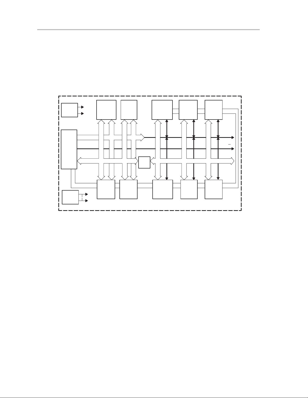
Introduction
2.1 Introduction
The architecture of the MSP430 family is based on a memory-to-memory
architecture, a common address space for all functional blocks, and a reduced
instruction set applicable to all functional blocks as illustrated in Figure 2–1.
See specific device data sheets for complete block diagrams of individual
devices.
Figure 2–1.MSP430 System Configuration
Oscillator
System
Clock
CPU
Incl.
16 Reg.
Random
Logic
ACLK
MCLK
MAB, 16 Bit
MDB, 16 Bit
Module Select
PROGRAM
Watchdog
2.2 Central Processing Unit
The CPU incorporates a reduced and highly transparent instruction set and a
highly orthogonal design. It consists of a 16-bit arithmetic logic unit (ALU), 16
registers, and instruction control logic. Four of these registers are used for
special purposes. These are the program counter (PC), stack pointer (SP),
status register (SR), and constant generator (CGx). All registers, except the
constant-generator registers R3/CG2 and part of R2/CG1, can be accessed
using the complete instruction set. The constant generator supplies instruction
constants, and is not used for data storage. The addressing mode used on
CG1 separates the data from the constants.
DATA I/O Port I/O Port I/O Port
Bus
Conv.
Timer_B
Comparator USART
USART
MAB, 4 Bit
R/W
MDB, 8 Bit
2-2
The CPU control over the program counter, the status register, and the stack
pointer (with the reduced instruction set) allows the development of
applications with sophisticated addressing modes and software algorithms.
Page 29

2.3 Program Memory
Instruction fetches from program memory are always 16-bit accesses,
whereas data memory can be accessed using word (16-bit) or byte (8-bit)
instructions. Any access uses the 16-bit memory data bus (MDB) and as many
of the least-significant address lines of the memory address bus (MAB) as
required to access the memory locations. Blocks of memory are automatically
selected through module-enable signals. This technique reduces overall
current consumption. Program memory is integrated as programmable or
mask-programmed memory.
In addition to program code, data may also be placed in the ROM section of
the memory map and may be accessed using word or byte instructions; this
is useful for data tables, for example. This unique feature gives the MSP430
an advantage over other microcontrollers, because the data tables do not
have to be copied to RAM for usage.
Sixteen words of memory are reserved for reset and interrupt vectors at the
top of the 64-kilobytes address space from 0FFFFh down to 0FFE0h.
Program Memory
2.4 Data Memory
The data memory is connected to the CPU through the same two buses as the
program memory (ROM): the memory address bus (MAB) and the memory
data bus (MDB). The data memory can be accessed with full (word) data width
or with reduced (byte) data width.
Additionally, because the RAM and ROM are connected to the CPU via the
same busses, program code can be loaded into and executed from RAM. This
is another unique feature of the MSP430 devices, and provides valuable,
easy-to-use debugging capability.
2.5 Operation Control
The operation of the different MSP430 members is controlled mainly by the
information stored in the special–function registers (SFRs). The different bits
in the SFRs enable interrupts, provide information about the status of interrupt
flags, and define the operating modes of the peripherals. By disabling
peripherals that are not needed during an operation, total current consumption
can be reduced. The individual peripherals are described later in this manual.
Architectural Overview
2-3
Page 30
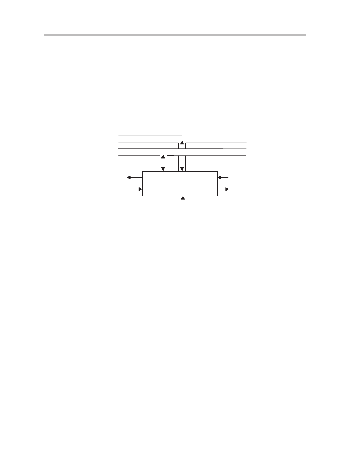
Peripherals
2.6 Peripherals
Peripheral modules are connected to the CPU through the MAB, MDB, and
interrupt service and request lines. The MAB is usually a 5-bit bus for most of
the peripherals. The MDB is an 8-bit or 16-bit bus. Most of the peripherals
operate in byte format. Modules with an 8-bit data bus are connected by
bus-conversion circuitry to the 16-bit CPU. The data exchange with these
modules must be handled with byte instructions. The SFRs are also handled
with byte instructions. The operation for 8-bit peripherals follows the order
described in Figure 2–2.
Figure 2–2.Bus Connection of Modules/Peripherals
MAB
MDB
Interrupt Request
Module/Peripheral
Interrupt Bus Grant
2.7 Oscillator and Clock Generator
The LFXT1 oscillator is designed for the commonly used 32,768 Hz,
low-current- consumption clock crystal or to be used with a high-speed crystal.
All analog components for the 32,768 Hz oscillator are integrated into the
MSP430; only the crystal needs to be connected with no other external
components required. When using the LFXT1 oscillator with a high-speed
crystal, additional load capacitors are required. Some MSP430 devices have
an additional high-speed crystal oscillator (LFXT2). Refer to the clock chapter
and the specific device data sheets for details.
In addition to the crystal oscillator(s), all MSP430 devices contain a digitallycontrolled RC oscillator (DCO). The DCO is different from RC oscillators found
on other microcontrollers because it is digitally controllable and tuneable.
Interrupt Request
Interrupt Bus Grant
PUC
2-4
Clock source selection for peripherals and CPU is very flexible. Most
peripherals are capable of using the 32768-Hz crystal oscillator clock, the
high-speed crystal oscillator clock (where applicable), or the DCO clock. The
CPU is capable of executing from the DCO clock or from either of the two
crystal oscillator clocks. See Chapter 7 for details on the clock system.
Page 31

Chapter 3
System Resets, Interrupts,
and Operating Modes
This chapter discusses the MSP430x1xx system resets, interrupts, and operating modes.
Topic Page
3.1 System Reset and Initialization 3-2. . . . . . . . . . . . . . . . . . . . . . . . . . . . . . . . .
3.2 Global Interrupt Structure 3-5. . . . . . . . . . . . . . . . . . . . . . . . . . . . . . . . . . . . .
3.3 MSP430 Interrupt-Priority Scheme 3-6. . . . . . . . . . . . . . . . . . . . . . . . . . . . . .
3.4 Interrupt Processing 3-9. . . . . . . . . . . . . . . . . . . . . . . . . . . . . . . . . . . . . . . . . .
3.5 Operating Modes 3-16. . . . . . . . . . . . . . . . . . . . . . . . . . . . . . . . . . . . . . . . . . . . .
3.6 Basic Hints for Low-Power Applications 3-22. . . . . . . . . . . . . . . . . . . . . . .
System Resets, Interrupts, and Operating Modes
3-1
Page 32

System Reset and Initialization
3.1 System Reset and Initialization
3.1.1 Introduction
The MSP430 system reset circuitry (shown in Figure 3–1) sources two internal
reset signals: power-on reset (POR) and power-up clear (PUC). Different
events trigger these reset signals and different initial conditions exist
depending on which signal was generated.
Figure 3–1.Power-On Reset and Power-Up Clear Schematic
V
V
CC
CC
POR Delay
POR
Detect
0 V
RST/MNI
NMI(WDTCTL.5)
TIMSEL
WDTQn
WDTIFG
EQU
KEYV
(from flash module)
†
From watchdog timer peripheral module
S
POR
S
Latch
R
0 V0 V
Delay
†
†
†
†
†
Resetwd1
Resetwd2
S
S
S
S
S
R
POR
Latch
MCLK
POR
PUC_DCO
PUC
A POR is a device reset. It is only generated by the two following events:
-
Powering up the device
-
A low signal on the RST/NMI pin when configured in the reset mode
A PUC is always generated when a POR is generated, but a POR is not
generated by a PUC. The following events trigger a PUC:
3-2
-
A POR signal
-
Watchdog timer expiration (in watchdog mode only)
-
Watchdog timer security key violation
-
A low signal on the RST/NMI pin when configured in the NMI mode
-
A Flash memory security key violation
Note:
If desired, software can cause a PUC by simply writing to the watchdog timer
control register with an incorrect password.
Page 33

Note:
Generation of the POR/PUC signals does not necessarily generate a system
reset interrupt. Anytime a POR is activated, a system reset interrupt is
generated. However, when a PUC is activated, a system reset interrupt may
or may not be generated. Instead, a lower priority interrupt vector may be
generated, depending on what action caused the PUC. Each device data
sheet gives a detailed table of what action generates each interrupt. This
table should be consulted for the proper handling of all interrupts.
When the VCC supply provides a fast rise time as shown in Figure 3–2, the
POR delay provides enough active time on the POR signal to allow the signal
to initialize the circuitry correctly after power up. When the V
slow, as shown in Figure 3–3, the POR detector holds the POR signal active
until Vcc has risen above the V
level. This also ensures a correct
(POR)
initialization.
Figure 3–2.Power-On Reset Timing on Fast VCC Rise Time
V
System Reset and Initialization
rise time is
CC
V
CC
POR
t
POR_Delay
If power to the chip is cycled, the supply voltage VCC must fall below the V
(see Figure 3–3) to ensure that another POR signal occurs when VCC is
powered up again. If VCC does not fall below V
a POR is not generated and power-up conditions do not set correctly.
Figure 3–3.Power-on Reset Timing on Slow VCC Rise Time
V
V
CC
V
(POR)
No POR
V
(min)
POR
during a cycle or a glitch,
(min)
POR
t
(min)
t
System Resets, Interrupts, and Operating Modes
3-3
Page 34

System Reset and Initialization
3.1.2 Device Initialization After System Reset
After a device reset (POR/PUC combination), the initial system conditions are:
-
I/O pins switched to input mode (see note below).
-
I/O flags are cleared as described in the I/O chapter (see note below).
-
Other peripherals and registers initialized as described in their respective
chapters.
-
Status register is reset.
-
Program counter is loaded with address contained at reset vector location
(0FFFEh). CPU execution begins at that address.
Note:
I/O pins and flags are only initialized after power-up. After the ’430 is
powered and running, if a reset is generated with RST/NMI pin (in reset
mode), the I/O pins are unaffected.
After a system reset, the user program can evaluate the various flags to
determine the source of the reset and take appropriate action.
The initial state of registers and peripherals is discussed in each applicable
section of this manual. Each register is shown with a key indicating the
rw–(0)
accessibility of the register and the initial condition, for example,
rw–0
. In these examples, the r indicates read, the w indicates write, and the
, or
value after the dash indicates the initial condition. If the value is in parenthesis,
the initial condition takes effect only after a POR – a PUC alone will not effect
the bit(s). If the value is not in parenthesis, it takes effect after a PUC alone or
after a POR/PUC combination. Some examples follow:
Type Description
rw–(0) Read/write, reset with POR
rw–0 Read/write, reset with POR or PUC
r–1 Read only, set with POR or PUC
r Read only, no initial state
w Write only, no initial state
3-4
Page 35

3.2 Global Interrupt Structure
There are four types of interrupts:
-
System reset
-
Maskable
-
Non-maskable
-
(Non)-maskable
System reset (POR/PUC) is discussed in section 3.1.
Maskable interrupts are caused by:
-
A watchdog-timer overflow (if timer mode is selected)
-
Other modules with interrupt capability
Non-maskable interrupts are not maskable in any way. No individual interrupt
enable bit is implemented for them, and the general interrupt enable bit (GIE)
has no effect on them.
(Non)-maskable interrupts are not masked by the general interrupt enable bit
(GIE) but are individually enabled or disabled by an individual interrupt enable
bit. When a (non)-maskable interrupt is accepted, the corresponding interrupt
enable bit is automatically reset, therefore disabling the interrupt for execution
of the interrupt service routine (ISR). The RETI (return from interrupt)
instruction has no effect on the individual enable bits of the (non)-maskable
interrupts. So the software must set the corresponding interrupt enable bit in
the ISR before execution of the RETI instruction for the interrupt to be
re-enabled after the ISR.
Global Interrupt Structure
A (non)-maskable NMI interrupt can be generated by an edge on the RST/NMI
pin (if NMI mode is selected), an oscillator fault occurs (if the oscillator fault
interrupt is enabled), or an access violation to the flash memory takes place
(if the access violation interrupt is enabled).
System Resets, Interrupts, and Operating Modes
3-5
Page 36

MSP430 Interrupt-Priority Scheme
3.3 MSP430 Interrupt-Priority Scheme
The interrupt priority of the modules, as shown in Figure 3–4, is defined by the
arrangement of the modules in the connection chain: the nearer a module is
to the CPU/NMIRS, the higher the priority.
Figure 3–4.Interrupt Priority Scheme
Priority
High
GMIRS
Low
CPU
PUC
Flash Security Key
PUC
Circuit
WDT Security Key
GIE
NMIRS
OSCfault
Flash ACCV
Reset/NMI
MAB – 5LSBs
Module
1
Module
2
12 12 12 12 1
Bus
Grant
WD
Timer
Module
m
Module
Reset and NMI, as shown in Figure 3–5, can only be used as alternative
interrupts because they use the same input pin. The associated control bits are
located in the watchdog timer control register shown in Figure 3–6, and are
password protected.
n
3-6
Page 37

Figure 3–5.Block Diagram of NMI Interrupt Sources
ACCV
ACCVIFG
S
FCTL1.1
MSP430 Interrupt-Priority Scheme
IE1.5
PUC
RST/NMI
IFG1.4
PUC
IE1.4
PUC
OSCFault
IFG1.1
IE1.1
PUC
Clear
S
Clear
Clear
S
Clear
ACCVIE
NMIFG
NMIIE
OFIFG
OFIE
NMI_IRQA
Counter
NMITMSELNMIES
WDT
IFG1.0
POR
IRQA
TIMSEL
IE1.0
Flash Module
Flash Module
POR PUC
KEYV
System Reset
Generator
WDTQn EQU
S
Clear
Clear
WDTIFG
WDTIE
Flash Module
VCC
PUC
POR
NMIRS
PUC POR
IRQ
IRQA: Interrupt Request Accepted
Watchdog Timer Module
PUC
System Resets, Interrupts, and Operating Modes
3-7
Page 38

MSP430 Interrupt-Priority Scheme
Figure 3–6.RST/NMI Mode Selection
70
WDTCTL
0120h
rw-0 rw-0 rw-0 rw-0 (w)-0 rw-0 rw-0 rw-0
NMIESHOLD NMI TMSEL CNTCL SSEL IS1 IS0
BITS 0–4,7 See Watchdog Timer chapter.
BIT 5: The NMI bit selects the function of the RST/NMI input pin. It is cleared after
a PUC signal.
NMI = 0: The RST/NMI input works as reset input. As long as the
RST/NMI pin is held low, the internal PUC signal is active
(level-sensitive).
NMI = 1: The RST
/NMI input works as an edge-sensitive, nonmaskable
interrupt input.
BIT 6: This bit selects the activating edge of the RST/NMI input if the NMI function
is selected. It is cleared after a PUC signal.
NMIES = 0: A rising edge triggers an NMI interrupt.
NMIES = 1: A falling edge triggers an NMI interrupt.
3.3.1 Operation of Global Interrupt—Reset/NMI
If the RST/NMI pin is set to the reset function, the CPU is held in the reset state
as long as the RST/NMI pin is held low. After the input changes to a high state,
the CPU starts program execution at the word address stored in word location
0FFFEh (reset vector).
If the RST/NMI pin is set to the NMI function, a signal edge (selected by the
NMIES bit) will generate an interrupt if the NMIIE bit is set. When accepted,
program execution begins at the address stored in location 0FFFCh. The RST
NMI flag in the SFR IFG1.4 is also set.
Note:
When configured in the NMI mode, a signal generating an NMI event should
not hold the RST
/NMI pin low, unless it is intended to hold the processor in
reset. When an NMI event occurs on the pin, the PUC signal is activated, thus
resetting the bits in the WDTCTL register. This results in the RST
/NMI pin
being configured in the reset mode. If the signal on the RST/NMI pin that
generated the NMI event remains low, the processor will be held in the reset
state.
When NMI mode is selected and the NMI edge select bit is changed, an NMI
can be generated, depending on the actual level at RST/NMI pin. When the
NMI edge select bit is changed before selecting the NMI mode, no NMI is
generated.
/
3-8
The NMI interrupt is maskable by the NMIIE bit.
Page 39

3.3.2 Operation of Global Interrupt—Oscillator Fault Control
The oscillator fault signal warns of a possible error condition with the crystal
oscillator.
3.3.2.1 Oscillator Fault Control in the Basic Clock System
The oscillator-fault signal is triggered when the LFXT1 oscillator is configured
to run in HF mode but is not running, stops running after being operational, or
is switched off. The oscillator-fault signal is also triggered under the same
conditions for the XT2 oscillator, present in some devices. Note that a PUC signal can trigger an oscillator fault, because the PUC switches the LFXT1 to LF
mode, therefore switching off the HF mode. The PUC signal also switches off
the XT2 oscillator.
The oscillator fault signal can be enabled to generate an NMI by bit OFIE in
the SFRs. The interrupt flag OFIFG in the SFRs can then be tested by the
interrupt service routine to determine if the NMI was caused by an oscillator
fault. See Basic Clock Module chapter for more details on the operation of the
crystal oscillators LFXT1 and XT2.
Interrupt Processing
3.4 Interrupt Processing
The MSP430 programmable interrupt structure allows flexible on-chip and
external interrupt configurations to meet real-time interrupt-driven system
requirements. Interrupts may be initiated by the processor’s operating
conditions such as watchdog overflow; or by peripheral modules or external
events. Each interrupt source can be disabled individually by an interrupt
enable bit, or all maskable interrupts can be disabled by the general interrupt
enable (GIE) bit in the status register.
Whenever an interrupt is requested and the appropriate interrupt enable bit
and general interrupt enable (GIE) bit are set, the interrupt service routine
becomes active as follows:
1) CPU active: The currently executing instruction is completed.
2) CPU stopped: The low-power modes are terminated.
3) The program counter pointing to the next instruction is pushed onto the
stack.
4) The status register is pushed onto the stack.
5) The interrupt with the highest priority is selected if multiple interrupts
occurred during the last instruction and are pending for service.
6) The appropriate interrupt request flag resets automatically on singlesource flags. Multiple source flags remain set for servicing by software.
7) The GIE bit is reset; the CPUOff bit, the OscOff bit, and the SCG1 bit are
cleared; the status bits V , N, Z, and C are reset. SCG0 is left unchanged.
System Resets, Interrupts, and Operating Modes
3-9
Page 40

Interrupt Processing
8) The content of the appropriate interrupt vector is loaded into the program
counter: the program continues with the interrupt handling routine at that
address.
The interrupt latency is six cycles, starting with the acceptance of an interrupt
request, and lasting until the start of execution of the appropriate
interrupt-service routine first instruction, as shown in Figure 3–7.
Figure 3–7.Interrupt Processing
Before
Interrupt
Item1
SP TOS
Item2
SP TOS
After
Interrupt
Item1
Item2
PC
SR
The interrupt handling routine terminates with the instruction:
RETI (return from an interrupt service routine)
which performs the following actions:
1) The status register with all previous settings pops from the stack. All previous settings of GIE, CPUOFF, etc. are now in effect, regardless of the
settings utilized during the interrupt service routine.
2) The program counter pops from the stack and begins execution at the
point where it was interrupted.
The return from the interrupt is illustrated in Figure 3–8.
Figure 3–8.Return From Interrupt
SP TOS
A RETI instruction takes five cycles. Interrupt nesting is activated if the GIE bit
is set inside the interrupt handling routine. The GIE bit is located in status
register SR/R2, which is included in the CPU as shown in Figure 3–9.
3-10
Before After
Return From Interrupt
Item1
Item2
PC
SR
SP TOS
Item1
Item2
PC
SR
Page 41

Figure 3–9.Status Register (SR)
15 0
Reserved For Future Enhancements
Apart from the GIE bit, other sources of interrupt requests can be enabled/
disabled individually or in groups. The interrupt enable flags are located
together within two addresses of the special-function registers (SFRs). The
program-flow conditions on interrupt requests can be easily adjusted using the
interrupt enable masks. The hardware serves the highest priority within the
empowered interrupt source.
87
SCG1V
rw-0
CPU
SCG0 GIE Z C
OSC
Off
Off
3.4.1 Interrupt Control Bits in Special-Function Registers (SFRs)
Most of the interrupt control bits, interrupt flags, and interrupt enable bits are
collected in SFRs under a few addresses, as shown in Table 3–1. The SFRs
are located in the lower address range and are implemented in byte format.
SFRs must be accessed using byte instructions.
Interrupt Processing
N
Table 3–1.Interrupt Control Bits in SFRs
Address 7 0
000Fh Not yet defined or implemented
000Eh Not yet defined or implemented
000Dh Not yet defined or implemented
000Ch Not yet defined or implemented
000Bh Not yet defined or implemented
000Ah Not yet defined or implemented
0009h Not yet defined or implemented
0008h Not yet defined or implemented
0007h Not yet defined or implemented
0006h Not yet defined or implemented
0005h Module enable 2 (ME2.x)
0004h Module enable 1 (ME1.x)
0003h Interrupt flag reg. 2 (IFG2.x)
0002h Interrupt flag reg. 1 (IFG1.x)
0001h Interrupt enable 2 (IE2.x)
0000h Interrupt enable 1 (IE1.x)
The MSP430 family supports SFRs by applying the correct logic and functions
to each individual module. Each module interrupt source can be individually
enabled or disable using the bits described in Table 3–2.
The interrupt-flag registers are described in Table 3–3. The module-enable
bits are described in Table 3–4.
System Resets, Interrupts, and Operating Modes
3-11
Page 42

Interrupt Processing
Table 3–2.Interrupt Enable Registers 1 and 2
Bit Position Short Form Initial State†Comments
IE1.0 WDTIE Reset Watchdog timer enable signal. Inactive if watchdog mode is
selected. Active if watchdog timer is configured as general-purpose
timer.
IE1.1 OFIE Reset Oscillator fault interrupt enable
IE1.2 Not implemented
IE1.3 Not implemented
IE1.4 NMIIE Reset NMI interrupt enable
IE1.5 ACCVIE Reset Flash access violation enable
IE1.6 URXIE0 Reset USART0 receive interrupt enable (13x, 14x devices)
IE1.7 UTXIE0 Reset USART0 transmit interrupt enable (13x, 14x devices)
IE2.0 Not implemented
IE2.1 Not implemented
IE2.2 Not implemented
IE2.3 Not implemented
IE2.4 URXIE1 Reset USART1 receive interrupt enable (14x devices)
IE2.5 UTXIE1 Reset USART1 transmit interrupt enable (14x devices)
IE2.6 Not implemented
IE2.7 Not implemented
†
The initial state is the logical state after the PUC signal.
3-12
Page 43

Interrupt Processing
Table 3–3.Interrupt Flag Register 1 and 2
Bit Position Short Form Initial State Comments
IFG1.0 WDTIFG Set Set on watchdog timer overflow in watchdog mode or security key
violation.
Or reset Reset with VCC power-up, or a reset condition at the RST/NMI pin
in reset mode.
IFG1.1
IFG1.2 Not implemented
IFG1.3 Not implemented
IFG1.4 NMIIFG Reset Set through the RST/NMI pin
IFG1.5 Not implemented
IFG1.6 URXIFG0 Reset USART0 receive flag (13x, 14x devices)
IFG1.7 UTXIFG0 Set USART0 transmitter ready (13x, 14x devices)
IFG2.0 Not implemented
IFG2.1 Not implemented
IFG2.2 Not implemented
IFG2.3 Not implemented
IFG2.4 URXIFG1 Reset USART1 receive flag (14x devices)
IFG2.5 UTXIFG1 Set USART1 transmitter ready (14x devices)
IFG2.6 Not implemented
IFG2.7 Not implemented
OFIFG Set Flag set on oscillator fault
Note: The configuration of some MSP430 devices may dif fer slightly from those in above table. Refer to specific device data
sheets for individual configurations.
System Resets, Interrupts, and Operating Modes
3-13
Page 44

Interrupt Processing
Table 3–4.Module Enable Registers 1 and 2
Bit Position Short Form Initial State Comments
ME1.0 Reserved
ME1.1 Reserved
ME1.2 Reserved
ME1.3 Reserved
ME1.4 Reserved
ME1.5 Reserved
ME1.6 URXE0
USPIE0
ME1.7 UTXE0 Reset USART0 transmit enable (UART mode)
ME2.0 Reserved
ME2.1 Reserved
ME2.2 Reserved
ME2.3 Reserved
ME2.4 URXE1
USPIE1
ME2.5 UTXE1 Reset USART1 transmit enable (UART mode)
ME2.6 Reserved
ME2.7 Reserved
Note: The configuration of some MSP430 devices may dif fer slightly from those in above table. Refer to specific device data
sheets for individual configurations.
Reset
Reset
Reset
Reset
USART0 receiver enable (UART mode)
USART0 transmit and receive enable (SPI mode)
USART1 receiver enable (UART mode)
USART1 transmit and receive enable (SPI mode)
3-14
Page 45
3.4.2 Interrupt Vector Addresses
The interrupt vectors and the power-up starting address are located in the
ROM, using the address range 0FFFFh – 0FFE0h as described in Table 3–5.
The vector contains the 16-bit address of the appropriate interrupt handler
instruction sequence. The interrupt vectors for 14x devices are shown in T able
3–5 in decreasing order of priority . See device data sheet for interrupt vectors
for a specific device.
Table 3–5.Interrupt Sources, Flags, and Vectors of 14x Configurations
INTERRUPT SOURCE INTERRUPT FLAG SYSTEM
Power-up
External Reset
Watchdog
Flash memory
NMI
Oscillator Fault
Flash memory access violation
Timer_B7 BCCIFG0 (see Note 2) Maskable 0FFFAh 13
Timer_B7
Comparator_A CMPAIFG Maskable 0FFF6h 11
Watchdog timer WDTIFG Maskable 0FFF4h 10
USART0 receive URXIFG0 Maskable 0FFF2h 9
USART0 transmit UTXIFG0 Maskable 0FFF0h 8
ADC ADCIFG (see Notes 1 & 2) Maskable 0FFEEh 7
Timer_A3 CCIFG0 (see Note 2) Maskable 0FFECh 6
Timer_A3
I/O port P1 (eight flags)
USART1 receive URXIFG1 Maskable 0FFE6h 3
USART1 transmit UTXIFG1 0FFE4h 2
I/O port P2 (eight flags)
NOTES: 1. Multiple source flags
2. Interrupt flags are located in the module.
3. (Non)maskable: the individual interrupt-enable bit can disable an interrupt event, but the general-interrupt enable
can not disable it.
Note: Some MSP430 devices have different implementations, See device datasheet for details.
NMIIFG (see Notes 1 & 3)
ACCVIFG (see Notes 1 & 3)
P1IFG.0 (see Notes 1 & 2)
P1IFG.7 (see Notes 1 & 2)
P2IFG.0 (see Notes 1 & 2)
P2IFG.7 (see Notes 1 & 2)
WDTIFG
KEYV
(see Note 1)
OFIFG (see Notes 1 & 3)
BCCIFG1 to BCCIFG6
TBIFG (see Notes 1 & 2)
CCIFG1,
CCIFG2,
TAIFG (see Notes 1 & 2)
To
To
INTERRUPT
Reset 0FFFEh 15, highest
(Non)maskable
(Non)maskable
(Non)maskable
Maskable 0FFF8h 12
Maskable 0FFEAh 5
Maskable 0FFE8h 4
Maskable 0FFE2h 1
ADDRESS
Interrupt Processing
WORD
0FFFCh 14
0FFE0h 0, lowest
PRIORITY
3.4.2.1 External Interrupts
All eight bits of ports P1 and P2 are designed for interrupt processing of
external events. All individual I/O bits are independently programmable. Any
combinations of inputs, outputs, and interrupt conditions are possible. This
allows easy adaptation to different I/O configurations. See Chapter I/O Ports
for more details on I/O ports.
System Resets, Interrupts, and Operating Modes
3-15
Page 46

Operating Modes
3.5 Operating Modes
The MSP430 family was developed for ultralow-power applications and uses
different levels of operating modes. The MSP430 operating modes, shown in
Figure 3–10, give advanced support to various requirements for ultralow
power and ultralow energy consumption. This support is combined with an
intelligent management of operations during the different module and CPU
states. An interrupt event wakes the system from each of the various operating
modes and the RETI instruction returns operation to the mode that was
selected before the interrupt event.
The ultra-low power system design which uses complementary metal-oxide
semiconductor (CMOS) technology , takes into account three different needs:
-
-
-
There are four bits that control the CPU and the main parts of the operation
of the system clock generator: CPUOff, OscOff, SCG0, and SCG1. These four
bits support discontinuous active mode (AM) requests, to limit the time period
of the full operating mode, and are located in the status register. The major
advantage of including the operating mode bits in the status register is that the
present state of the operating condition is saved onto the stack during an
interrupt service request. As long as the stored status register information is
not altered, the processor continues (after RETI) with the same operating
mode as before the interrupt event. Another program flow may be selected by
manipulating the data stored on the stack or the stack pointer. Being able to
access the stack and stack pointer with the instruction set allows the program
structures to be individually optimized, as illustrated in the following program
flow:
The desire for speed and data throughput despite conflicting needs for
ultra-low power
Minimization of individual current consumption
Limitation of the activity state to the minimum required by the use of low
power modes
3-16
-
Enter interrupt routine
The interrupt routine is entered and processed if an enabled interrupt awakens
the MSP430:
J
The SR and PC are stored on the stack, with the content present at the
interrupt event.
J
Subsequently, the operation mode control bits OscOff, SCG1, and
CPUOff are cleared automatically in the status register.
Page 47

Operating Modes
-
Return from interrupt
Two dif ferent modes are available to return from the interrupt service routine
and continue the flow of operation:
J
Return with low-power mode bits set. When returning from the
interrupt, the program counter points to the next instruction. The
instruction pointed to is not executed, since the restored low power
mode stops CPU activity.
J
Return with low-power mode bits reset. When returning from the
interrupt, the program continues at the address following the
instruction that set the OscOff or CPUOff-bit in the status register . To
use this mode, the interrupt service routine must reset the OscOff,
CPUOff, SCGO, and SCG1 bits on the stack. Then, when the SR
contents are popped from the stack upon RETI, the operating mode
will be active mode (AM).
There are six operating modes that the software can configure:
-
Active mode AM; SCG1=0, SCG0=0, OscOff=0, CPUOff=0:
CPU clocks are active
-
Low power mode 0 (LPM0); SCG1=0, SCG0=0, OscOff=0, CPUOff=1:
CPU is disabled
MCLK is disabled
SMCLK and ACLK remain active
-
Low power mode 1 (LPM1); SCG1=0, SCG0=1, OscOff=0, CPUOff=1:
CPU is disabled
MCLK is disabled
DCO’s dc generator is disabled if the DCO is not used for MCLK or
SMCLK when in active mode. Otherwise, it remains enabled.
SMCLK and ACLK remain active
System Resets, Interrupts, and Operating Modes
3-17
Page 48

Operating Modes
-
Low power mode 2 (LPM2); SCG1=1, SCG0=0, OscOff=0, CPUOff=1:
CPU is disabled
MCLK is disabled
SMCLK is disabled
DCO oscillator automatically disabled because it is not needed for MCLK
or SMCLK
DCO’s dc-generator remains enabled
ACLK remains active
-
Low power mode 3 (LPM3); SCG1=1, SCG0=1, OscOff=0, CPUOff=1:
CPU is disabled
MCLK is disabled
SMCLK is disabled
DCO oscillator is disabled
DCO’s dc-generator is disabled
ACLK remains active
-
Low power mode 4 (LPM4); SCG1=X, SCG0=X, OscOff=1, CPUOff=1:
CPU is disabled
ACLK is disabled
MCLK is disabled
SMCLK is disabled
DCO oscillator is disabled
DCO’s dc-generator is disabled
Crystal oscillator is stopped
Note:
Peripheral operation is not halted by CPUOff. Peripherals are controlled by
their individual control registers.
3-18
Page 49

Table 3–6.Low Power Mode Logic Chart for Basic Clock System
SCG1 SCG0 OscOff CPUOff
LPM0 0 0 0 1
LPM1 0 1 0 1
LPM2 1 0 0 1
LPM3 1 1 0 1
LPM4 1 1 1 1
These modes are illustrated in Figure 3–11.
Figure 3–10. MSP430x1xx Operating Modes For Basic Clock System
Operating Modes
WDT Active,
Time Expired, Overflow
WDT Active,
Security Key Violation
CPUOff = 1
SCG0,1 = 0
LP Mode LPM0
CPU Off, MCLK Off,
SMCLK, ACLK On
CPUOff = 1
SCG0 = 1
SCG1 = 0
LP Mode LPM1
CPU Off, MCLK Off,
SMCLK, ACLK On
DC Generator Off if DCO
not used in active mode
RST/NMI
Reset Active
POR
WDTIFG = 1
WDTIFG = 1
V arious Modules Are Active
CPUOff = 1
SCG0 = 0
SCG1 = 1
CPU Off, MCLK Off,
SMCLK Off, DCO Off,
PUC
Active Mode
CPU Is Active
LP Mode LPM2
ACLK On
VCC On
WDTIFG = 0
/NMI is Reset Pin
RST
WDT is Active
CPUOff = 1
SCG0,1 = 1
RST/NMI
NMI Active
CPUOff = 1
OscOff = 1
SG0,1 = 1
LP-Mode LPM4
CPU Off, MCLK Off,
DCO Off, ACLK Off
DC Generator Off
LP Mode LPM3
CPU Off, MCLK Off,
SMCLK Off, DCO Off
ACLK On
DC Generator Off
System Resets, Interrupts, and Operating Modes
3-19
Page 50

Operating Modes
Figure 3–11. Typical Current Consumption of 13x and 14x Devices vs. Operating Modes
90
45
340
225
70
65
0
AM
LPM0 LPM2 LPM3 LPM4
315
270
225
Aµ
180
135
ICC/
The low-power modes 1–4 enable or disable the CPU and the clocks. In
addition to the CPU and clocks, enabling or disabling specific peripherals may
further reduce total current consumption of the individual modes. The activity
state of each peripheral is controlled by the control registers for the individual
peripherals. In addition, the SFRs include module enable bits that may be used
to enable or disable the operation of specific peripheral modules (see
Table 3–4).
3.5.1 Low-Power Mode 0 and 1 (LPM0 and LPM1)
Low power mode 0 or 1 is selected if bit CPUOff in the status register is set.
Immediately after the bit is set the CPU stops operation, and the normal
operation of the system core stops. The operation of the CPU halts and all
internal bus activities stop until an interrupt request or reset occurs. The
system clock generator continues operation, and the clock signals MCLK,
SMCLK, and ACLK stay active depending on the state of the other three status
register bits, SCG0, SCG1, and OscOff.
17
11
Operating Modes
2
VCC = 3 V
= 2.2 V
V
CC
1
0.1 0.1
3-20
The peripherals are enabled or disabled with their individual control register
settings, and with the module enable registers in the SFRs. All I/O port pins
and RAM/registers are unchanged. Wake up is possible through all enabled
interrupts.
The following are examples of entering and exiting LPM0. The method shown
is applicable to all low-power modes.
The following example describes entering into low-power mode 0.
;===Main program flow with switch to CPUOff Mode==============
;
BIS #18h,SR ;Enter LPM0 + enable general interrupt GIE
;(CPUOff=1, GIE=1). The PC is incremented
;during execution of this instruction and
;points to the consecutive program step.
...... ;The program continues here if the CPUOff
;bit is reset during the interrupt service
;routine. Otherwise, the PC retains its
;value and the processor returns to LPM0.
Page 51

The following example describes clearing low-power mode 0.
;===Interrupt service routine=================================
...... ;CPU is active while handling interrupts
BIC #10h,0(SP) ;Clears the CPUOff bit in the SR contents
;that were stored on the stack.
RETI ;RETI restores the CPU to the active state
;because the SR values that are stored on
;the stack were manipulated. This occurs
;because the SR is pushed onto the stack
;upon an interrupt, then restored from the
;stack after the RETI instruction.
3.5.2 Low-Power Modes 2 and 3 (LPM2 and LPM3)
Low-power mode 2 or 3 is selected if bits CPUOff and SCG1 in the status
register are set. Immediately after the bits are set, CPU, MCLK, and SMCLK
operations halt and all internal bus activities stop until an interrupt request or
reset occurs.
Peripherals that operate with the MCLK or SMCLK signal are inactive because
the clock signals are inactive. Peripherals that operate with the ACLK signal
are active or inactive according with the individual control registers and the
module enable bits in the SFRs. All I/O port pins and the RAM/registers are
unchanged. Wake up is possible by enabled interrupts coming from active
peripherals or RST
/NMI.
Operating Modes
3.5.3 Low-Power Mode 4 (LPM4)
In low power mode 4 all activities cease; only the RAM contents, I/O ports, and
registers are maintained. Wake up is only possible by enabled external
interrupts.
Before activating LPM4, the software should consider the system conditions
during the low power mode period . The two most important conditions are
environmental (that is, temperature effect on the DCO), and the clocked
operation conditions.
The environment defines whether the value of the frequency integrator should
be held or corrected. A correction should be made when ambient conditions
are anticipated to change drastically enough to increase or decrease the
system frequency while the device is in LPM4.
System Resets, Interrupts, and Operating Modes
3-21
Page 52

Basic Hints for Low-Power Applications
3.6 Basic Hints for Low-Power Applications
There are some basic practices to follow when current consumption is a critical
part of a system application:
-
Switch off analog circuitry when possible.
-
Select the lowest possible operating frequency for the core and the
individual peripheral module.
-
Use the interrupt driven software; the program starts execution rapidly.
-
Tie all unused inputs to an applicable voltage level. The list below defines
the correct termination for all unused pins.
-
AVCC:
-
AVSS:
-
Xout:
-
XIN
-
XT2IN
-
XT2OUT
-
Px.0 to Px.7:
-
RST/NMI:
-
Test/V
-
Test
-
TDO:
-
TDI:
-
TMS:
-
TCK:
Pin
PP
Potential Comment
DV
CC
DV
SS
open
DV
SS
DV
SS
open 13x and 14x devices
open Unused ports switched to port function and
resp.VCCPullup resistor 100k
DV
CC
DV
SS
DV
SS
Refer to device specific datasheets for the correct termination of these pins.
13x and 14x devices
output direction
11x devices
11x1 devices
3-22
Page 53

Chapter 4
Memory
MSP430 devices are configured as a von-Neumann architecture. It has code
memory , data memory , and peripherals in one address space. As a result, the
same instructions are used for code, data, or peripheral accesses. Also, code
may be executed from RAM.
Topic Page
4.1 Introduction 4-2. . . . . . . . . . . . . . . . . . . . . . . . . . . . . . . . . . . . . . . . . . . . . . . . . .
4.2 Data in the Memory 4-3. . . . . . . . . . . . . . . . . . . . . . . . . . . . . . . . . . . . . . . . . . .
4.3 Internal ROM Organization 4-4. . . . . . . . . . . . . . . . . . . . . . . . . . . . . . . . . . . . .
4.4 RAM and Peripheral Organization 4-6. . . . . . . . . . . . . . . . . . . . . . . . . . . . . .
Memory
4-1
Page 54

Introduction
4.1 Introduction
All of the physically separated memory areas (ROM, RAM, SFRs, and
peripheral modules) are mapped into the common address space, as shown
in Figure 4–1 for the MSP430 family . The addressable memory space is 64KB.
Future expansion is possible.
Figure 4–1.Memory Map of Basic Address Space
Address
(Hex.)
0FFFFh
0FFE0h
0FFDFh
0200h
01FFh
0100h
0FFh
010h
0Fh
0h
Interrupt Vector Table
Program Memory
Branch Control Tables
Data Tables...
Data Memory
16-Bit Peripheral Modules
8-Bit Peripheral Modules
Special Function Registers
Function
ROM
ROM
RAM
Timer,
ADC, . . .
I/O, LCD
8bT/C, . . .
SFR
Access
Word/Byte
Word/Byte
Word/Byte
Word
Byte
Byte
The memory data bus (MDB) is 16- or 8-bits wide. For those modules that can
be accessed with word data the width is always 16 bits. For the other modules,
the width is 8 bits, and they must be accessed using byte instructions only . The
program memory (ROM) and the data memory (RAM) can be accessed with
byte or word instructions.
Figure 4–2.Memory Data Bus
Address Range 0000h – 00FFh
LCD USART ROM RAM
SFRs COMPARATOR_A
8-Bit Peripheral Modules,
Byte Access
4-2
High Byte
Data Bus
Low Byte
Byte/Word
Access
CPU
ADC WDT
16-Bit Peripheral Modules,
Word Access
Page 55

4.2 Data in the Memory
Bytes are located at even or odd addresses as shown in Figure 4–3. However,
words are only located at even addresses. Therefore, when using word
instructions, only even addresses may be used. The low byte of a word is
always at an even address. The high byte of a word is at the next odd address
after the address of the word. For example, if a data word is located at address
xxx2h, then the low byte of that data word is located at address xxx2h, and the
high byte of that word is located at address xxx3h.
Figure 4–3.Bits, Bytes, and Words in a Byte-Organized Memory
Data in the Memory
xxxAh
157146. . Bits . .
. . Bits . .9180
Byte
Byte
Word (High Byte)
Word (Low Byte)
xxx9h
xxx8h
xxx7h
xxx6h
xxx5h
xxx4h
xxx3h
Memory
4-3
Page 56
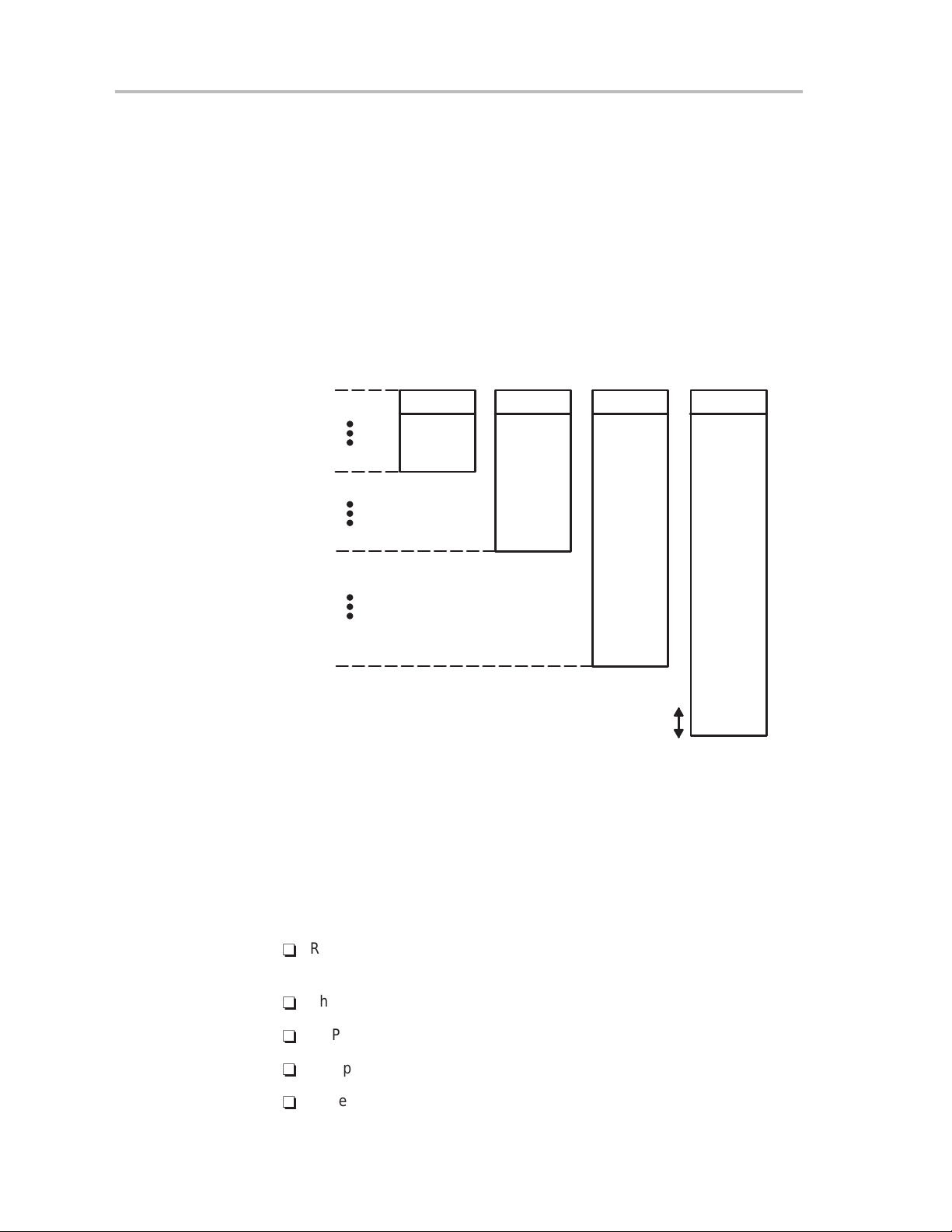
Internal ROM Organization
4.3 Internal ROM Organization
V arious sizes of ROM (OTP , masked-ROM, EPROM, or FLASH) are available
within the 64-kB address space, as shown in Figure 4–4. The common
address space is shared with SFRs, peripheral module registers, data and
code memory . The SFRs and peripheral modules are mapped into the address
range, starting with 0 and ending with 01FFh. The remaining address space,
0200h to 0FFFFh, is shared by data and code memory . The start address for
ROM depends on the amount of ROM present. The interrupt vector table is
mapped into the the upper 16 words of ROM address space, with the highest
priority interrupt vector at the highest ROM word address (0FFFEh). See the
individual data sheets for specific memory maps.
Figure 4–4.ROM Organization
0FFFEh
0FFE0h
0F000h
0EFFFh
0D000h
0CFFFh
08000h
4.3.1 Processing of ROM Tables
The MSP430 architecture allows for the storage and usage of large tables in
ROM without the need to copy the tables to RAM before using them. This ROM
accessing of tables allows fast and clear programming in applications where
data tables are necessary . This offers the flexible advantages listed below, and
saves on ROM and RAM requirements. To access these tables, all word and
byte instructions can be used.
4 k
12 k
32 k
VectorsVectors Vectors Vectors
Vectors
xx k
4-4
-
ROM storage of an output programmable logic array (OPLA) for display
character conversion
-
The use of as many OPLA terms as needed (no restriction on n terms)
-
OTP version automatically includes OPLA programmability
-
Computed table accessibility (for example, for a bar graph display)
-
Table-supported program flows
Page 57

4.3.2 Computed Branches and Calls
Computed branches and subroutine calls are possible using standard
instructions. The call and branch instructions use the same addressing modes
as the other instructions.
The addressing modes allow indirect-indirect addressing that is ideally suited
for computed branches and calls. This programming technique permits a
program structure that is different from conventional 8- and 16-bit
microcontrollers. Most of the routines can be handled easily by using software
status handling instead of flag-type program-flow control.
The computed branch and subroutine calls are valid throughout the entire
ROM space.
Internal ROM Organization
Memory
4-5
Page 58

RAM and Peripheral Organization
4.4 RAM and Peripheral Organization
The entire RAM can be accessed with byte or word instructions using the
appropriate instruction suffix. The peripheral modules, however, are located
in two different address spaces and must be accessed with the appropriate
instruction length.
-
The SFRs are byte-oriented and mapped into the address space from 0h
up to 0Fh.
-
Peripheral modules that are byte-oriented are mapped into the address
space from 010h up to 0FFh.
-
Peripheral modules that are word-oriented are mapped into the address
space from 100h up to 01FFh.
4.4.1 Random Access Memory
RAM can be used for both code and data memory . Code accesses are always
performed on even byte addresses.
The instruction mnemonic suffix defines the data as being word or byte data.
Example:
MOV.B TXDATA,&UTXBUF0 ;Byte access
ADD R5,SUM_A = ADD.W R5,SUM_A ;Word access
ADDC SUM_B = ADDC.W SUM_A ;Word access
A word consists of two bytes: a high byte (bit 15 to bit 8), and a low byte
(bit 7 to bit 0) as shown in Figure 4–5. It must always align to an even address.
Figure 4–5.Byte and Word Operation
Byte1: 012h
Byte2: 034h
Word1 (High Byte): 056h
Word1 (Low Byte): 078h
Word2 (High Byte): 09Ah
Word2 (Low Byte): 0BCh
xxxAh
ADD.B Byte1, Byte2:
xxx9h
Byte2 = 012h + 034h = 046h
xxx8h
xxx7h
xxx6h
ADD.W Word1, Word2:
Word2 = 05678h + 09ABCh = 0F134h
xxx5h
xxx4h
4-6
xxx3h
All operations on the stack and PC are word operations and use even-aligned
memory addresses.
Page 59

RAM and Peripheral Organization
In the following examples, word-to-word and byte-to-byte operations show the
results of the operation and the status bit information.
Example Word-Word Operation Example Byte-Byte Operation
R5 = 0F28Eh R5 = 0223h
EDE .EQU 0212h EDE .EQU 0202h
Mem(0F28Eh) = 0FFFEh Mem(0223h) = 05Fh
Mem(0212h) = 00112h Mem(0202h) = 043h
ADD @R5,&EDE ADD.B @R5,&EDE
Mem(0212h) = 00110h Mem(0202h) = 0A2h
C = 1, Z = 0, N = 0 C = 0, Z = 0, N = 1
Figure 4–6 shows the register-byte and byte-register operations.
Figure 4–6.Register
-Byte/Byte-Register Operations
Register-Byte Operation
High Byte Low Byte
Unused
Byte
Register
Memory
Byte-Register Operation
High Byte Low Byte
Byte
0h
Memory
Register
The following examples describe the register-byte and byte-register
operations.
Example Register-Byte Operation Example Byte-Register Operation
R5 = 0A28Fh R5 = 01202h
R6 = 0203h R6 = 0223h
Mem(0203h) = 012h Mem(0223h) = 05Fh
ADD.B R5,0(R6) ADD.B @R6,R5
08Fh 05Fh
+ 012h + 002h ;Low byte of R5
0A1h
00061h ;–>Store into R5
;High byte is 0
Mem (0203h) = 0A1h R5 = 00061h
C = 0, Z = 0, N = 1 C = 0, Z = 0, N = 0
(Low byte of register) (Addressed byte)
+ (Addressed byte) + (Low byte of register)
–>(Addressed byte)
–>(Low byte of register,
zero to High byte)
Memory
4-7
Page 60

RAM and Peripheral Organization
Note: Word-Byte Operations
Word-byte or byte-word operations on memory data are not supported. Each
register-byte or byte-register is performed as a byte operation.
4.4.2 Peripheral Modules—Address Allocation
Some peripheral modules are accessible only with byte instructions, while
others are accessible only with word instructions. The address space from
0100 to 01FFh is reserved for word modules, and the address space from 00h
to 0FFh is reserved for byte modules.
Peripheral modules that are mapped into the word address space must be
accessed using word instructions (for example, MOV R5,&WDTCTL).
Peripheral modules that are mapped into the byte address space must be
accessed with byte instructions (MOV.B #1,&P1OUT).
The addressing of both is through the absolute addressing mode or the 16-bit
working registers using the indexed, indirect, or indirect autoincrement
addressing mode. See Figure 4–7 for the RAM/peripheral organization.
Figure 4–7.Example of RAM/Peripheral Organization
Address
(Hex.)
01FFh
0100h
0FFh
010h
0Fh
0h
4.4.2.1 Word Modules
70
16-Bit Peripheral Modules
8-Bit Peripheral Modules
Special Function Registers
Word modules are peripherals that are connected to the 16-bit MDB.
Word modules can be accessed with word or byte instructions. If byte
instructions are used, only even addresses are permissible, and the high byte
of the result is always ’0’.
The peripheral file address space is organized into sixteen frames with each
frame representing eight words as described in Table 4–1.
Function
Timer,
ADC, . . .
I/O, USART
Comparator_A, . . .
SFR
Access
Word
Byte
Byte
4-8
Page 61

Table 4–1.Peripheral File Address Map—Word Modules
Address Description
1F0h – 1FFh Reserved
1E0h – 1EFh Reserved
1D0h – 1DFH Reserved
1C0h – 1CFH Reserved
1B0h – 1BFH Reserved
1A0h – 1AFH ADC12 control and interrupt
190h – 19FH Timer_B
180h – 18FH Timer_B
170h – 17FH Timer_A
160h – 16FH Timer_A
150h – 15FH ADC12 conversion
140h – 14FH ADC12 conversion
130h – 13FH Multiplier
120h – 12FH Watchdog Timer, Flash control
110h – 11FH Reserved
100h – 10FH
Reserved
RAM and Peripheral Organization
4.4.2.2 Byte Modules
Byte modules are peripherals that are connected to the reduced (eight LSB)
MDB. Access to byte modules is always by byte instructions. The hardware
in the peripheral byte modules takes the low byte (the LSBs) during a write
operation.
Byte instructions operate on byte modules without any restrictions. Read
access to peripheral byte modules using word instructions results in
unpredictable data in the high byte. Word data is written into a byte module by
writing the low byte to the appropriate peripheral register and ignoring the high
byte.
The peripheral file address space is organized into sixteen frames as
described in Table 4–2.
Memory
4-9
Page 62

RAM and Peripheral Organization
Table 4–2.Peripheral File Address Map—Byte Modules
Address Description
00F0h – 00FFh Reserved
00E0h – 00EFh Reserved
00D0h – 00DFh Reserved
00C0h – 00CFh Reserved
00B0h – 00BFh Reserved
00A0h – 00AFh Reserved
0090h – 009Fh Reserved
0080h – 008Fh ADC12 memory control
0070h – 007Fh USART0, USART1
0060h – 006Fh Reserved
0050h – 005Fh System clock generator, Comparator A
0040h – 004Fh Reserved
0030h – 003Fh Digital I/O port P5, digital I/O port P6
0020h – 002Fh Digital I/O port P1 and P2 control
0010h – 001Fh Digital I/O port P3, and P4 control
0000h – 000Fh
Special function
4.4.3 Peripheral Modules-Special Function Registers (SFRs)
The system configuration and the individual reaction of the peripheral modules
to the processor operation is configured in the SFRs as described in
Table 4–3. The SFRs are located in the lower address range, and are
organized by bytes. SFRs must be accessed using byte instructions only.
4-10
Page 63

Table 4–3.Special Function Register Address Map
Address Data Bus
000Fh Not yet defined or implemented
000Eh Not yet defined or implemented
000Dh Not yet defined or implemented
000Ch Not yet defined or implemented
000Bh Not yet defined or implemented
000Ah Not yet defined or implemented
0009h Not yet defined or implemented
0008h Not yet defined or implemented
0007h Not yet defined or implemented
0006h Not yet defined or implemented
0005h Module enable 2; ME2.2
0004h Module enable 1; ME1.1
0003h Interrupt flag reg. 2; IFG2.x
0002h Interrupt flag reg.1; IFG1.x
0001h Interrupt enable 2; IE2.x
0000h Interrupt enable 1; IE1.x
RAM and Peripheral Organization
70
The system power consumption is influenced by the number of enabled
modules and their functions. Disabling a module from the actual operation
mode reduces power consumption while other parts of the controller remain
fully active (unused pins must be tied appropriately or power consumption will
increase; see
Basic Hints for Low Power Applications
in section 3.6.
Memory
4-1 1
Page 64

4-12
Page 65

Chapter 5
16-Bit CPU
The MSP430 von-Neumann architecture has RAM, ROM, and peripherals in
one address space, both using a single address and data bus. This allows
using the same instruction to access either RAM, ROM, or peripherals and
also allows code execution from RAM.
Topic Page
5.1 CPU Registers 5-2. . . . . . . . . . . . . . . . . . . . . . . . . . . . . . . . . . . . . . . . . . . . . . . .
5.2 Addressing Modes 5-7. . . . . . . . . . . . . . . . . . . . . . . . . . . . . . . . . . . . . . . . . . . .
5.3 Instruction Set Overview 5-17. . . . . . . . . . . . . . . . . . . . . . . . . . . . . . . . . . . . .
5.4 Instruction Map 5-23. . . . . . . . . . . . . . . . . . . . . . . . . . . . . . . . . . . . . . . . . . . . . .
16-Bit CPU
5-1
Page 66

CPU Registers
R2
5.1 CPU Registers
Sixteen 16-bit registers (R0, R1, and R4 to R15) are used for data and
addresses and are implemented in the CPU. They can address up to
64 Kbytes (ROM, RAM, peripherals, etc.) without any segmentation. The
complete CPU-register set is described in Table 5–1. Registers R0, R1, R2,
and R3 have dedicated functions, which are described in detail later.
Table 5–1.Register by Functions
Program counter (PC) R0
Stack pointer (SP) R1
Status register (SR)
Constant generator (CG1)
Constant generator (CG2) R3
Working register R4 R4
Working register R5 R5
: :
: :
Working register R13 R13
Working register R14 R14
Working register R15 R15
5.1.1 The Program Counter (PC)
The 16-bit program counter points to the next instruction to be executed. Each
instruction uses an even number of bytes (two, four, or six), and the program
counter is incremented accordingly. Instruction accesses are performed on
word boundaries, and the program counter is aligned to even addresses.
Figure 5–1 shows the program counter bits.
Figure 5–1.Program Counter
15 0
Program Counter Bits 15 to 1
5.1.2 The System Stack Pointer (SP)
The system stack pointer must always be aligned to even addresses because
the stack is accessed with word data during an interrupt request service. The
system SP is used by the CPU to store the return addresses of subroutine calls
and interrupts. It uses a predecrement, postincrement scheme. The
advantage of this scheme is that the item on the top of the stack is available.
The SP can be used by the user software (PUSH and POP instructions), but
the user should remember that the CPU also uses the SP. Figure 5–2 shows
the system SP bits.
1
0
Figure 5–2.System Stack Pointer
15 0
System Stack Pointer Bits 15 to 1
5-2
1
0
Page 67

5.1.2.1 Examples for System SP Addressing (Refer to Figure 5–4)
MOV SP,R4 ; SP –> R4
MOV @SP,R5 ; Item I3 (TOS) –> R5
MOV 2(SP),R6 ; Item I2 –> R6
MOV R7,0(SP) ; Overwrite TOS with R7
MOV R8,4(SP) ; Modify item I1
PUSH R12 ; Store R12 in address 0xxxh – 6; SP points to same address
POP R12 ; Restore R12 from address 0xxxh – 6; SP points to
0xxxh – 4
MOV @SP+,R5 ; Item I3 –> R5 (popped from stack); same as POP
instruction
Figure 5–3 shows stack usage.
Figure 5–3.Stack Usage
PUSH #1 POP R8Address
CPU Registers
0xxxh
0xxxh – 2
0xxxh – 4
0xxxh – 6
0xxxh – 8
I1
I2
I3
5.1.2.2 Special Cases—PUSH SP and POP SP
The special cases of using the SP as an argument to the PUSH and POP
instructions are described below.
Figure 5–4.PUSH SP and POP SP
PUSH SP
SP
old
SP
1
The stack pointer is changed after
a PUSH SP instruction.
SP
1
SP
I1
I2
I3
#1
SP
The stack pointer is not changed
after a POP SP instruction.
SP
2
I1
I2
I3
POP SP
SP
1
SP
After the sequence
PUSH SP
I
I
POP SP ; SP2 is stack pointer after this instruction
; SP1 is stack pointer after this instruction
The stack pointer is two bytes lower than before this sequence.
16-Bit CPU
5-3
Page 68
CPU Registers
5.1.3 The Status Register (SR)
The status register SR contains the following CPU status bits:
-
V Overflow bit
-
SCG1 System clock generator control bit 1
-
SCG0 System clock generator control bit 0
-
OscOff Crystal oscillator off bit
-
CPUOff CPU off bit
-
GIE General interrupt enable bit
-
N Negative bit
-
Z Zero bit
-
C Carry bit
Figure 5–5 shows the SR bits.
Figure 5–5.Status Register Bits
15 0
Reserved For Future Enhancements
879
CPU
SCG1V
rw-0
SCG0 GIE Z C
OSC
Off
Off
N
Table 5–2 describes the status register bits.
Table 5–2.Description of Status Register Bits
Bit Description
V Overflow bit. Set if the result of an arithmetic operation overflows the signed-variable range. The
bit is valid for both data formats, byte and word:
ADD(.B), ADDC(.B) Set when:
Positive + Positive = Negative
Negative + Negative = Positive, otherwise reset
SUB(.B), SUBC(.B), CMP(.B) Set when:
Positive – Negative = Negative
Negative – Positive = Positive, otherwise reset
SCG1, SCG0 These bits control four activity states of the system-clock generator and therefore influence the
operation of the processor system.
OscOFF If set, the crystal oscillator enters off mode: all activities cease; however, the RAM contents, the
port, and the registers are maintained. Wake up is possible only through enabled external
interrupts when the GIE bit is set and from the NMI.
CPU Off If set, the CPU enters off mode: program execution stops. However , the RAM, the port registers,
and especially the enabled peripherals (for example, Timer_A, UART, etc.) stay active. Wake
up is possible through all enabled interrupts.
GIE If set, all enabled maskable interrupts are handled. If reset, all maskable interrupts are disabled.
The GIE bit is cleared by interrupts and restored by the RETI instruction as well as by other
appropriate instructions.
N Set if the result of an operation is negative.
Word operation: Negative bit is set to the value of bit 15 of the result
Byte operation: Negative bit is set to the value of bit 7 of the result
Z Set if the result of byte or word operation is 0; cleared if the result is not 0.
C
Set if the result of an operation produced a carry; cleared if no carry occurred. Some instructions
modify the carry bit using the inverted zero bits.
5-4
Page 69

Note: Status Register Bits V, N, Z, and C
The status register bits V , N, Z, and C are modified only with the appropriate
instruction. For additional information, see the detailed description of the
instruction set in Appendix B.
5.1.4 The Constant Generator Registers CG1 and CG2
Commonly-used constants are generated with the constant generator
registers R2 and R3, without requiring an additional 16-bit word of program
code. The constant used for immediate values is defined by the addressing
mode bits (As) as described in T able 5–3. See Section 5.3 for a description of
the addressing mode bits (As).
Table 5–3.Values of Constant Generators CG1, CG2
Register As Constant Remarks
R2 00 – – – – – Register mode
R2 01 (0) Absolute address mode
R2 10 00004h +4, bit processing
R2 11 00008h +8, bit processing
R3 00 00000h 0, word processing
R3 01 00001h +1
R3 10 00002h +2, bit processing
R3 11 0FFFFh –1, word processing
CPU Registers
The major advantages of this type of constant generation are:
-
No special instructions required
-
Reduced code memory requirements: no additional word for the six most
used constants
-
Reduced instruction cycle time: no code memory access to retrieve the
constant
The assembler uses the constant generator automatically if one of the six
constants is used as a source operand in the immediate addressing mode.
The status register SR/R2, used as a source or destination register, can be
used in the register mode only. The remaining combinations of
addressing-mode bits are used to support absolute-address modes and bit
processing without any additional code. Registers R2 and R3, used in the
constant mode, cannot be addressed explicitly; they act like source-only
registers.
16-Bit CPU
5-5
Page 70

CPU Registers
The RISC instruction set of the MSP430 only has 27 instructions. However, the
constant generator allows the MSP430 assembler to support 24 additional,
emulated instructions. For example, the single-operand instruction:
CLR dst
is emulated by the double-operand instruction with the same length:
MOV R3,dst
or the equivalent
MOV #0,dst
where #0 is replaced by the assembler, and R3 is used with As = 00, which
results in:
-
One word instruction
-
No additional control operation or hardware within the CPU
-
Register-addressing mode for source: no additional fetch cycle for the
constant (#0)
5-6
Page 71

5.2 Addressing Modes
All seven addressing modes for the source operand and all four addressing
modes for the destination operand can address the complete address space.
The bit numbers in T able 5–4 describe the contents of the As and Ad mode bits.
See Section 5.3 for a description of the source address As and the destination
address Ad bits.
Table 5–4.Source/Destination Operand Addressing Modes
As/Ad Addressing Mode Syntax Description
00/0 Register mode Rn Register contents are operand
01/1 Indexed mode X(Rn) (Rn + X) points to the operand
01/1 Symbolic mode ADDR (PC + X) points to the operand
01/1 Absolute mode &ADDR The word following the instruction
10/– Indirect register
mode
11/– Indirect
autoincrement
1 1/–
Immediate mode #N The word following the instruction
@Rn Rn is used as a pointer to the
@Rn+ Rn is used as a pointer to the
Addressing Modes
X is stored in the next word
X is stored in the next word.
Indexed mode X(PC) is used.
contains the absolute address.
operand.
operand. Rn is incremented
afterwards.
contains the immediate constant
N. Indirect autoincrement mode
@PC+ is used.
The seven addressing modes are explained in detail in the following sections.
Most of the examples show the same addressing mode for the source and
destination, but any valid combination of source and destination addressing
modes is possible in an instruction.
16-Bit CPU
5-7
Page 72

Addressing Modes
5.2.1 Register Mode
The register mode is described in Table 5–5.
Table 5–5.Register Mode Description
Assembler Code Content of ROM
MOV R10,R11 MOV R10,R11
Length: One or two words
Operation: Move the content of R10 to R11. R10 is not affected.
Comment: Valid for source and destination
Example: MOV R10,R1 1
Before: After:
R1 1
PC
0A023hR10
0FA15h
PC
old
R1 1
PC PC
0A023hR10
0A023h
+ 2
old
Note: Data in Registers
The data in the register can be accessed using word or byte instructions. If
byte instructions are used, the high byte is always 0 in the result. The status
bits are handled according to the result of the byte instruction.
5-8
Page 73

5.2.2 Indexed Mode
The indexed mode is described in Table 5–6.
Table 5–6.Indexed Mode Description
Assembler Code Content of ROM
MOV 2(R5),6(R6) MOV X(R5),Y(R6)
Length: Two or three words
Operation: Move the contents of the source address (contents of R5 + 2)
Comment: Valid for source and destination
Addressing Modes
X = 2
Y = 6
to the destination address (contents of R6 + 6). The source
and destination registers (R5 and R6) are not affected. In
indexed mode, the program counter is incremented
automatically so that program execution continues with the
next instruction.
Example: MOV 2(R5),6(R6):
Before:
0FF16h
0FF14h
0FF12h
01094h
01092h
01090h
01084h
01082h
01080h
Address
Space
00006h
00002h
04596h PC
0xxxxh
05555h
0xxxxh
0xxxxh
01234h
0xxxxh
Register
R5
R6
01080h
0108Ch
0108Ch
+0006h
01092h
01080h
+0002h
01082h
After:
0FF16h
0FF14h
0FF12h
01094h
01092h
01090h
01084h
01082h
01080h
Address
Space
0xxxxh
00006h
00002h
04596h
0xxxxh
01234h
0xxxxh
0xxxxh
01234h
0xxxxh
PC
Register
R5
R6
01080h
0108Ch
16-Bit CPU
5-9
Page 74

Addressing Modes
5.2.3 Symbolic Mode
The symbolic mode is described in Table 5–7.
Table 5–7.Symbolic Mode Description
Assembler Code Content of ROM
MOV EDE,TONI MOV X(PC),Y(PC)
Length: Two or three words
Operation: Move the contents of the source address EDE (contents of
PC + X) to the destination address TONI (contents of PC + Y).
The words after the instruction contain the differences
between the PC and the source or destination addresses.
The assembler computes and inserts offsets X and Y
automatically . With symbolic mode, the program counter (PC)
is incremented automatically so that program execution
continues with the next instruction.
X = EDE – PC
Y = TONI – PC
Comment: Valid for source and destination
Example: MOV EDE,TONI ;Source address EDE = 0F016h,
;dest. address TONI=01114h
Before:
0FF16h
0FF14h
0FF12h
0F018h
0F016h
0F014h
01116h
01114h
01112h
Address
Space
011FEh
0F102h
04090h PC
0xxxxh
0A123h
0xxxxh
0xxxxh
01234h
0xxxxh
Register
0FF14h
+0F102h
0F016h
0FF16h
+011FEh
01114h
After:
0FF16h
0FF14h
0FF12h
0F018h
0F016h
0F014h
01116h
01114h
01112h
Address
Space
0xxxxh
011FEh
0F102h
04090h
0xxxxh
0A123h
0xxxxh
0xxxxh
0A123h
0xxxxh
Register
PC
5-10
Page 75

5.2.4 Absolute Mode
The absolute mode is described in Table 5–8.
Table 5–8.Absolute Mode Description
Assembler Code Content of ROM
MOV &EDE,&TONI MOV X(0),Y(0)
Length: Two or three words
Operation: Move the contents of the source address EDE to the
destination address TONI. The words after the instruction
contain the absolute address of the source and destination
addresses. With absolute mode, the PC is incremented
automatically so that program execution continues with the
next instruction.
Comment: Valid for source and destination
Example: MOV &EDE,&TONI ;Source address EDE = 0F016h,
Addressing Modes
X = EDE
Y = TONI
;dest. address TONI=01114h
Before:
0FF16h
0FF14h
0FF12h
0F018h
0F016h
0F014h
01116h
01114h
01112h
Address
Space
01114h
0F016h
04292h PC
0xxxxh
0A123h
0xxxxh
0xxxxh
01234h
0xxxxh
Register
After:
0FF16h
0FF14h
0FF12h
0F018h
0F016h
0F014h
01116h
01114h
01112h
Address
Space
0xxxxh
01114h
0F016h
04292h
0xxxxh
0A123h
0xxxxh
0xxxxh
0A123h
0xxxxh
Register
PC
This address mode is mainly for hardware peripheral modules that are located
at an absolute, fixed address. These are addressed with absolute mode to
ensure software transportability (for example, position-independent code).
16-Bit CPU
5-11
Page 76
Addressing Modes
5.2.5 Indirect Mode
The indirect mode is described in table 5–9.
Table 5–9.Indirect Mode Description
Assembler Code Content of ROM
MOV @R10,0(R11) MOV @R10,0(R11)
Length: One or two words
Operation: Move the contents of the source address (contents of R10) to
Comment: Valid only for source operand. The substitute for destination
Example: MOV.B @R10,0(R11)
the destination address (contents of R11). The registers are
not modified.
operand is 0(Rd).
Before:
0FF16h
0FF14h
0FF12h
0FA34h
0FA32h
0FA30h
002A8h
002A7h
002A6h
Address
Space
0xxxxh
0000h
04AEBh
0xxxxh
0xxxxh
05BC1h
0xxxxh
0xxh
012h
0xxh
PC
R10
R1 1
Register
0FA33h
002A7h
After:
0FF16h
0FF14h
0FF12h
0FA34h
0FA32h
0FA30h
002A8h
002A7h
002A6h
Address
Space
0xxxxh
0000h
04AEBh
0xxxxh
0xxxxh
05BC1h
0xxxxh
0xxh
05Bh
0xxh
PC
R10
R1 1
Register
0FA33h
002A7h
5-12
Page 77

5.2.6 Indirect Autoincrement Mode
The indirect autoincrement mode is described in Table 5–10.
Table 5–10.Indirect Autoincrement Mode Description
Assembler Code Content of ROM
MOV @R10+,0(R11) MOV @R10+,0(R11)
Length: One or two words
Operation: Move the contents of the source address (contents of R10) to
the destination address (contents of R11). Register R10 is
incremented by 1 for a byte operation, or 2 for a word
operation after the fetch; it points to the next address without
any overhead. This is useful for table processing.
Comment: Valid only for source operand. The substitute for destination
operand is 0(Rd) plus second instruction INCD Rd.
Example: MOV @R10+,0(R1 1)
Addressing Modes
Before:
0FF18h
0FF16h
0FF14h
0FF12h
0FA34h
0FA32h
0FA30h
010AAh
010A8h
010A6h
Address
Space
0xxxxh
00000h
04ABBh
0xxxxh
0xxxxh
05BC1h
0xxxxh
0xxxxh
01234h
0xxxxh
PC
R10
R1 1
Register
0FA32h
010A8h
After:
0FF18h
0FF16h
0FF14h
0FF12h
0FA34h
0FA32h
0FA30h
010AAh
010A8h
010A6h
Address
Space
0xxxxh
00000h
04ABBh
0xxxxh
0xxxxh
05BC1h
0xxxxh
0xxxxh
05BC1h
0xxxxh
PC
R1 1
Register
0FA34hR10
010A8h
The autoincrementing of the register contents occurs after the operand is
fetched. This is shown in Figure 5–6.
Figure 5–6.Operand Fetch Operation
Instruction Address Operand
+1/ +2
16-Bit CPU
5-13
Page 78

Addressing Modes
5.2.7 Immediate Mode
The immediate mode is described in Table 5–11.
Table 5–11.Immediate Mode Description
Assembler Code Content of ROM
MOV #45,TONI MOV @PC+,X(PC)
Length: Two or three words
It is one word less if a constant of CG1 or CG2 can be used.
Operation: Move the immediate constant 45, which is contained in the
word following the instruction, to destination address TONI.
When fetching the source, the program counter points to the
word following the instruction and moves the contents to the
destination.
Comment: Valid only for a source operand.
45
X = TONI – PC
Example: MOV #45,TONI
Before:
0FF16h
0FF14h
0FF12h
010AAh
010A8h
010A6h
Address
Space
01192h
00045h
040B0h PC
0xxxxh
01234h
0xxxxh
Register
0FF16h
+01192h
010A8h
After:
0FF18h
0FF16h
0FF14h
0FF12h
010AAh
010A8h
010A6h
Address
Space
0xxxxh
01192h
00045h
040B0h
0xxxxh
00045h
0xxxxh
Register
PC
5-14
Page 79

5.2.8 Clock Cycles, Length of Instruction
The operating speed of the CPU depends on the instruction format and
addressing modes. The number of clock cycles refers to the MCLK.
5.2.8.1 Format-I Instructions
Table 5–12 describes the CPU format-I instructions and addressing modes.
Table 5–12.Instruction Format I and Addressing Modes
Addressing Modes
Address Mode
As Ad
00, Rn
00, Rn 1, x(Rm)
01, x(Rn)
01, EDE
01, &EDE
01, x(Rn)
01, EDE
01, &EDE
10, @Rn 0, Rm 2 1 AND @R4,R5
10, @Rn 1, x(Rm)
11, @Rn+
11, #N
11, @Rn+
11, #N
11, @Rn+
11, #N
0, Rm
0, PC
1, EDE
1, &EDE
0, Rm 3 2
1, x(Rm)
1, TONI
1, &TONI
1, EDE
1, &EDE
0, Rm
0, PC
0, Rm
0, PC
1, x(Rm)
1, EDE
1, &EDE
No. of Length of Example
Cycles Instruction
1
2
4 2
6 3
5 2
2
3
2
3
5 2
1
1
2
2
2
2
3
3
3
2
2
1
1
2
2
3
2
3
MOVBRR5,R8
R9
ADD
XOR
MOR
MOV
AND
MOV
ADD
CMP
MOV
ADD
XOR
MOV
XOR
ADD
BR
MOV
BR
MOV
ADD
MOV
ADD
R5,3(R6)
R8,EDE
R5,&EDE
2(R5),R7
EDE,R6
&EDE,R8
3(R4),6(R9)
EDE,TONI
2(R5),&TONI
EDE,&TONI
@R5,8(R6)
@R5,EDE
@R5,&EDE
@R5+,R6
@R9+
#20,R9
#2AEh
@R9+,2(R4)
#33,EDE
@R9+,&EDE
#33,&EDE
16-Bit CPU
5-15
Page 80

Addressing Modes
(
)
5.2.8.2 Format-II Instructions
Table 5–13 describes the CPU format II instructions and addressing modes.
Table 5–13.Instruction Format-II and Addressing Modes
No. of Cycles
RRA
RRC
Address Mode
A
s/d
00, Rn
01, X(Rn)
01, EDE
01, &EDE
10, @Rn 3 4 1 RRC @R9
11, @Rn+
(see Note)
11, #N
Note: Instruction Format II Immediate Mode
Do not use instructions RRA, RRC, SWPB, and SXT with the immediate
mode in the destination field. Use of these in the immediate mode will result
in an unpredictable program operation.
SWPB
SXT
1 3/4 1 SWPB R5
4
4
3 4/5 1
PUSH/
CALL
5
5
Length of
Instruction
(words)
2
2
2
Example
CALL 2(R7)
PUSH EDE
SXT &EDE
SWPB @R10+
CALL #81H
5.2.8.3 Format-III Instructions
Format-III instructions are described as follows:
Jxx—all instructions need the same number of cycles, independent of
whether a jump is taken or not.
Clock cycle: Two cycles
Length of instruction: One word
5.2.8.4 Miscellaneous-Format Instructions
Table 5–14 describes miscellaneous-format instructions.
Table 5–14.Miscellaneous Instructions or Operations
Activity Clock Cycle
RETI 5 cycles
Interrupt 6 cycles
WDT reset 4 cycles
Reset (RST/NMI) 4 cycles
†
Length of instruction
1 word
†
5-16
Page 81

5.3 Instruction Set Overview
This section gives a short overview of the instruction set. The addressing
modes are described in Section 5.2.
Instructions are either single or dual operand or jump.
The source and destination parts of an instruction are defined by the following
fields:
src The source operand defined by As and S-reg
dst The destination operand defined by Ad and D-reg
As The addressing bits responsible for the addressing mode used
for the source (src)
S-reg The working register used for the source (src)
Ad The addressing bits responsible for the addressing mode used
for the destination (dst)
D-reg The working register used for the destination (dst)
B/W Byte or word operation:
0: word operation
1: byte operation
Instruction Set Overview
Note: Destination Address
Destination addresses are valid anywhere in the memory map. However,
when using an instruction that modifies the contents of the destination, the
user must ensure the destination address is writeable. For example, a
masked-ROM location would be a valid destination address, but the contents
are not modifiable, so the results of the instruction would be lost.
16-Bit CPU
5-17
Page 82

Instruction Set Overview
5.3.1 Double-Operand Instructions
Figure 5–7 illustrates the double-operand instruction format.
Figure 5–7.Double Operand Instruction Format
15 0
Opcode
Table 5–15 describes the effects of an instruction on double operand
instruction status bits.
8714 13 12 11 10 9 6 5 4 3 2 1
B/W D-Reg
AdS-Reg
Table 5–15.Double Operand Instruction Format Results
Mnemonic S-Reg, D-Reg Operation Status Bits
MOV
ADD src,dst src + dst –> dst * * * *
ADDC src,dst src + dst + C –> dst * * * *
SUB src,dst dst + .not.src + 1 –> dst * * * *
SUBC src,dst dst + .not.src + C –> dst * * * *
CMP src,dst dst – src * * * *
DADD src,dst src + dst + C –> dst (dec) * * * *
AND src,dst src .and. dst –> dst 0 * * *
BIT src,dst src .and. dst 0 * * *
BIC src,dst .not.src .and. dst –> dst – – – –
BIS src,dst src .or. dst –> dst – – – –
XOR src,dst src .xor. dst –> dst * * * *
src,dst src –> dst – – – –
As
VNZC
* The status bit is affected
– The status bit is not affected
0 The status bit is cleared
1 The status bit is set
Note: Instructions CMP and SUB
The instructions CMP and SUB are identical except for the storage of the
result. The same is true for the BIT and AND instructions.
5-18
Page 83

5.3.2 Single-Operand Instructions
Figure 5–8 illustrates the single-operand instruction format.
Figure 5–8.Single Operand Instruction Format
15 0
8714 13 12 11 10 9 6 5 4 3 2 1
Instruction Set Overview
Opcode
B/W D/S-Reg
Table 5–16 describes the effects of an instruction on the single operand
instruction status bits.
Table 5–16.Single Operand Instruction Format Results
Mnemonic S-Reg, D-Reg Operation Status Bits
RRC
RRA dst MSB –> MSB –>....LSB –> C 0 * * *
PUSH src SP – 2 –> SP, src –> @ SP – – – –
SWPB dst swap bytes – – – –
CALL dst SP – 2 –> SP – – – –
RETI TOS –> SR, SP <– SP + 2 X X X X
SXT dst Bit 7 –> Bit 8........Bit 15 0 * * *
dst C –> MSB –>.......LSB –> C * * * *
PC+2 –> stack, dst –> PC
TOS –> PC, SP <– SP + 2
* The status bit is affected
– The status bit is not affected
0 The status bit is cleared
1 The status bit is set
Ad
VNZC
All addressing modes are possible for the CALL instruction. If the symbolic
mode (ADDRESS), the immediate mode (#N), the absolute mode (&EDE) or
the indexed mode X (RN) is used, the word that follows contains the address
information.
16-Bit CPU
5-19
Page 84

Instruction Set Overview
5.3.3 Conditional Jumps
Conditional jumps support program branching relative to the program counter.
The possible jump range is from –511 to +512 words relative to the program
counter state of the jump instruction. The 10-bit program-counter offset value
is treated as a signed 10-bit value that is doubled and added to the program
counter. None of the jump instructions affect the status bits.
The instruction code fetch and the program counter increment technique end
with the formula:
PC
new
= PC
+ 2 + PC
old
Figure 5–9 shows the conditional-jump instruction format.
Figure 5–9.Conditional-Jump Instruction Format
15 0
Opcode
C 10-Bit PC Offset
Table 5–17 describes these conditional-jump instructions.
8714 13 12 11 10 9 6 5 4 3 2 1
Table 5–17.Conditional-Jump Instructions
Mnemonic
JEQ/JZ Label Jump to label if zero bit is set
JNE/JNZ Label Jump to label if zero bit is reset
JC Label Jump to label if carry bit is set
JNC Label Jump to label if carry bit is reset
JN Label
JGE Label Jump to label if (N .XOR. V) = 0
JL Label Jump to label if (N .XOR. V) = 1
JMP Label Jump to label unconditionally
S-Reg, D-Reg
× 2
offset
Operation
Jump to label if negative bit is set
5-20
Page 85

Instruction Set Overview
5.3.4 Short Form of Emulated Instructions
The basic instruction set, together with the register implementations of the
program counter, stack pointer, status register, and constant generator, form
the emulated instruction set; these make up the popular instruction set. The
status bits are set according to the result of the execution of the basic
instruction that replaces the emulated instruction.
Table 5–18 describes these instructions.
Table 5–18.Emulated Instructions
Mnemonic Description Status Bits Emulation
VNZC
ArIthmetic Instructions
ADC[.W] dst Add carry to destination * * * * ADDC #0,dst
ADC.B dst Add carry to destination * * * * ADDC.B #0,dst
DADC[.W] dst Add carry decimal to destination * * * * DADD #0,dst
DADC.B dst Add carry decimal to destination * * * * DADD.B #0,dst
DEC[.W] dst Decrement destination * * * * SUB #1,dst
DEC.B dst Decrement destination * * * * SUB.B #1,dst
DECD[.W] dst Double-decrement destination * * * * SUB #2,dst
DECD.B dst Double-decrement destination * * * * SUB.B #2,dst
INC[.W] dst Increment destination * * * * ADD #1,dst
INC.B dst Increment destination * * * * ADD.B #1,dst
INCD[.W] dst Increment destination * * * * ADD #2,dst
INCD.B dst Increment destination * * * * ADD.B #2,dst
SBC[.W] dst Subtract carry from destination * * * * SUBC #0,dst
SBC.B dst Subtract carry from destination * * * * SUBC.B #0,dst
Logical Instructions
INV[.W] dst Invert destination * * * * XOR #0FFFFh,dst
INV.B dst Invert destination * * * * XOR.B #–1,dst
RLA[.W] dst Rotate left arithmetically * * * * ADD dst,dst
RLA.B dst Rotate left arithmetically * * * * ADD.B dst,dst
RLC[.W] dst Rotate left through carry * * * * ADDC dst,dst
RLC.B dst Rotate left through carry * * * * ADDC.B dst,dst
Data Instructions (common use)
CLR[.W] Clear destination – – – – MOV #0,dst
CLR.B Clear destination – – – – MOV.B #0,dst
CLRC Clear carry bit – – – 0 BIC #1,SR
CLRN Clear negative bit – 0 – – BIC #4,SR
CLRZ Clear zero bit – – 0 – BIC #2,SR
POP dst Item from stack – – – – MOV @SP+,dst
SETC Set carry bit – – – 1 BIS #1,SR
SETN Set negative bit – 1 – – BIS #4,SR
SETZ Set zero bit – – 1 – BIS #2,SR
16-Bit CPU
5-21
Page 86

Instruction Set Overview
Table 5–18. Emulated Instructions (Continued)
Mnemonic Description Status Bits Emulation
V N Z C
Data Instructions (common use) (continued)
TST[.W] dst Test destination 0 * * * CMP #0,dst
TST.B dst Test destination 0 * * * CMP.B #0,dst
Program Flow Instructions
BR dst Branch to . . . – – – – MOV dst,PC
DINT Disable interrupt – – – – BIC #8,SR
EINT Enable interrupt – – – – BIS #8,SR
NOP No operation – – – – MOV #0h,#0h
RET Return from subroutine – – – – MOV @SP+,PC
5.3.5 Miscellaneous
Instructions without operands, such as CPUOff, are not provided. Their
functions are switched on or off by setting or clearing the function bits in the
status register or the appropriate I/O register. Other functions are emulated
using dual operand instructions.
Some examples are as follows:
BIS #28h,SR ; Enter OscOff mode
; + Enable general interrupt (GIE)
BIS #18h,SR ; Enter CPUOff mode
; + Enable general interrupt (GIE)
5-22
Page 87

5.4 Instruction Map
The instruction map in Figure 5–10 is an example of how to encode
instructions. There is room for more instructions, if needed.
Figure 5–10. Core Instruction Map
000 040 080 0C0 100 140 180 1C0 200 240 280 2C0 300 340
0x
04x
08x
0Cx
RRC.B SWPB RRA RRA.B SXT PUSH PUSH.B CALL RETI
RRC
10x
14x
18x
1Cx
20x
24x
28x
2Cx
30x
34x
38x
3Cx
40x–4Fx
50x–5Fx
60x–6Fx
70x–7Fx
80x–8Fx
90x–9Fx
A0x–AFx
B0x–BFx
C0x–CFx
D0x–DFx
E0x–EFx
F0x–FFx
Instruction Map
380 3C0
JNE/JNZ
JEQ/JZ
JNC
JC
JN
JGE
JL
JMP
MOV, MOV.B
ADD, ADD.B
ADDC, ADDC.B
SUBC, SUBC.B
SUB, SUB.B
CMP, CMP.B
DADD, DADD.B
BIT, BIT.B
BIC, BIC.B
BIS, BIS.B
XOR, XOR.B
AND, AND.B
16-Bit CPU
5-23
Page 88

5-24
Page 89

Chapter 6
Hardware Multiplier
The hardware multiplier is a 16-bit peripheral module. It is not integrated into
the CPU. Therefore, it requires no special instructions and operates
independent of the CPU. To use the hardware multiplier, the operands are
loaded into registers and the results are available the next instruction—no
extra cycles are required for a multiplication.
Topic Page
6.1 Hardware Multiplier Module Support 6-2. . . . . . . . . . . . . . . . . . . . . . . . . . . .
6.2 Hardware Multiplier Operation 6-3. . . . . . . . . . . . . . . . . . . . . . . . . . . . . . . . .
6.3 Hardware Multiplier Registers 6-9. . . . . . . . . . . . . . . . . . . . . . . . . . . . . . . . . .
6.4 Hardware Multiplier Special Function Bits 6-10. . . . . . . . . . . . . . . . . . . . . .
6.5 Hardware Multiplier Software Restrictions 6-10. . . . . . . . . . . . . . . . . . . . .
Hardware Multiplier
6-1
Page 90

Hardware Multiplier Module Support
6.1 Hardware Multiplier Module Support
The hardware multiplier module expands the capabilities of the MSP430
family without changing the basic architecture. Multiplication is possible for:
-
16×16 bits
-
16×8 bits
-
8×16 bits
-
8×8 bits
The hardware multiplier module supports four types of multiplication: unsigned
multiplication (MPY), signed multiplication (MPYS), unsigned multiplication
with accumulation (MAC), and signed multiplication with accumulation
(MACS). Figure 6–1 shows how the hardware multiplier module interfaces
with the bus system to support multiplication operations.
Figure 6–1.Connection of the Hardware Multiplier Module to the Bus System
ROM RAM
TDI
TDO
TMS
TCK
CPU
Incl. 16 Reg.
Test
JTAG
MAB, 16 Bit
MDB, 16 Bit
MPY
MPYS
MAC
MACS
Other
Modules
6-2
Page 91

Hardware Multiplier Operation
6.2 Hardware Multiplier Operation
The hardware multiplier has two 16-bit registers for both operands and three
registers to store the results of the multiplication. The multiplication is
executed correctly when the first operand is written to the operand register
OP1 prior to writing the second operand to OP2. Writing the first operand to
the applicable register selects the type of multiplication. Writing the second
operand to OP2 starts the multiplication. Multiplication is completed before the
result registers are accessed using the indexed address mode for the source
operand. When indirect or indirect autoincrement address modes are used,
another instruction is needed between the writing of the second operand and
accessing the result registers. Both operands, OP1 and OP2, utilize all seven
address mode capabilities.
No instruction is necessary for the multiplication; as a result, the real-time
operation does not require additional clock cycles and the interrupt latency is
unchanged.
The multiplier architecture is illustrated in Figure 6–2.
Figure 6–2.Block Diagram of the MSP430 16×16-Bit Hardware Multiplier
0rw15
Operand 1
(address
defines
operation)
MPY 130h
MPYS 132h
MAC 134h
MACS 136h
Operand 1 Operand 2 138h
0rw15 0rw15
Mode
16 x 16 Multiplier
031
Accessible Register
0000
MACS
MPYS
MACMPY
Mode Mode
Multiplexer
SumExt 13Eh C
S
Product Register
MPY, MPYS
32-Bit Multiplexer
Accumulator ACC
SumLo 013AhSumHi 13Ch
32-Bit Adder
MAC, MACS
0rw150rw150r15
Hardware Multiplier
6-3
Page 92

Hardware Multiplier Operation
ACC) ≤
ACC) >
ACC) >
ACC) ≤
The sum extension register contents differ, depending on the operation and
on the results of the operation.
Table 6–1.Sum Extension Register Contents
Register MPY MPYS MAC MACS, see Notes
Operand1 x + – + +
(OP1×OP2 +
(OP1×OP2 +
(OP1×OP2 +
(OP1×OP2 +
Operand2 x + – – –
SumExt
Note: The following two overflow conditions may occur when using the MACS function and should be handled by software or
avoided.
0000h 0000h 0FFFFh 0000h 0001h 0FFFFh 0000h
1) The result of a MACS operation is positive and larger than 07FFF FFFFh. In this case, the SumExt register contains
0FFFFh and the ACC register contains a negative number (8000 0000h .... 0FFFF FFFFh).
2) The result of a MACS operation is negative and less than or equal to 07FFF FFFFh. In this case, the SumExt register
contains 0000h and the ACC register contains a positive number (0000 0000h ... 07FFF FFFFh).
0FFFFFFFFh
0FFFFFFFFh
07FFFFFFFh
07FFFFFFFh
6-4
Page 93

Hardware Multiplier Operation
6.2.1 Multiply Unsigned, 16×16 bit, 16× 8 bit, 8×16 bit, 8 ×8 bit
The following multiplication operation shows 32 bytes of program code and 32
execution cycles (16×16 bit multiplication).
**********************************************************
* TRANSFER BOTH OPERANDS TO THE REGISTERS IN THE *
* HARDWARE MULTIPLIER MODULE *
* USE CONSTANT OPERAND1 AND OPERAND2 TO IDENTIFY *
* BYTE DATA *
**********************************************************
OPERAND1 .EQU 0 ; 0: OPERAND1 IS WORD (16BIT)
; 8: OPERAND1 IS BYTE ( 8BIT)
OPERAND2 .EQU 0 ; 0: OPERAND2 IS WORD (16BIT)
; 8: OPERAND2 IS BYTE ( 8BIT)
MPY .EQU 0130H
MPYS .EQU 0132H
MAC .EQU 0134H
MACS .EQU 0136H
OP2 .EQU 0138H
RESLO .EQU 013AH
RESHI .EQU 013CH
SUMEXT .EQU 013EH
.BSS OPER1,2,200H
.BSS OPER2,2
.BSS RAM,8
.IF OPERAND1=8
MOV.B &OPER1,&MPY ; LOAD 1ST OPERAND,
; DEFINES ADD. UNSIGNED MULTIPLY
.ELSE
MOV &OPER1,&MPY ; LOAD 1ST OPERAND,
; DEFINES ADD. UNSIGNED MULTIPLY
.ENDIF
.IF OPERAND1=8
MOV.B &OPER2,&OP2 ; LOAD 2ND OPERAND AND START
; MULTIPLICATION
.ELSE
MOV &OPER2,&OP2 ; LOAD 2ND OPERAND AND START
; MULTIPLICATION
.ENDIF
**********************************************************
* EXAMPLE TO ADD THE RESULT OF THE HARDWARE *
* MULTIPLICATION TO THE RAM DATA, 64BITS *
**********************************************************
ADD &RESLO,&RAM ; ADD LOW RESULT TO RAM
ADDC &RESHI,&RAM+2 ; ADD HIGH RESULT TO RAM+2
ADC &RAM+4 ; ADD CARRY TO EXTENSION WORD
ADC &RAM+6 ; IF 64 BIT LENGTH IS USED
Hardware Multiplier
6-5
Page 94

Hardware Multiplier Operation
6.2.2 Multiply Signed, 16×16 bit, 16×8 bit, 8×16 bit, 8×8 bit
The following multiplication operation shows 36 bytes of program code and 36
execution cycles (16×16 bit multiplication).
**********************************************************
* TRANSFER BOTH OPERANDS TO THE REGISTERS IN THE *
* HARDWARE MULTIPLIER MODULE *
* IF ONE OF THE OPERANDS IS 8 BIT, SIGN EXTENSION *
* is NEEDED. USE CONSTANT OPERAND1 AND OPERAND2 TO *
* IDENTIFY BYTE DATA *
**********************************************************
OPERAND1 .EQU 0 ; 0: OPERAND1 IS WORD (16BIT)
; 8: OPERAND1 IS BYTE ( 8BIT)
OPERAND2 .EQU 0 ; 0: OPERAND2 IS WORD (16BIT)
; 8: OPERAND2 IS BYTE ( 8BIT)
MPY .EQU 0130H
MPYS .EQU 0132H
MAC .EQU 0134H
MACS .EQU 0136H
OP2 .EQU 0138H
RESLO .EQU 013AH
RESHI .EQU 013CH
SUMEXT .EQU 013EH
.BSS OPER1,2,200H
.BSS OPER2,2
.BSS RAM,8
.IF OPERAND1=0
MOV &OPER1,&MPYS ; LOAD 1ST (WORD) OPERAND,
; DEFINES ADD. SIGNED MULTIPLY
.ELSE
MOV.B &OPER1,&MPYS ; LOAD 1ST (BYTE) OPERAND,
; DEFINES ADD. SIGNED MULTIPLY
SXT &MPYS ; EXPAND BYTE TO SIGNED WORD DATA
.ENDIF
.IF OPERAND2=0
MOV &OPER2,&OP2 ; LOAD 2ND (WORD) OPERAND AND
; START SIGNED MULTIPLICATION
.ELSE
MOV.B &OPER2,&OP2 ; LOAD 2ND (BYTE) OPERAND,
SXT &OP2 ; RE–LOAD 2ND OPERAND AND START
; SIGNED ‘FINAL’ MULTIPLICATION
.ENDIF
**********************************************************
* EXAMPLE TO ADD THE RESULT OF THE HARDWARE *
* MULTIPLICATION TO THE RAM DATA, 64 BITS *
**********************************************************
ADD &RESLO,&RAM ; ADD LOW RESULT TO RAM
ADDC &RESHI,&RAM+2 ; ADD HIGH RESULT TO RAM+2
ADDC &SUMEXT,&RAM+4 ; ADD SIGN WORD TO EXTENSION WORD
ADDC &SUMEXT,&RAM+6 ; IF 64 BIT LENGTH IS USED
6-6
Page 95

Hardware Multiplier Operation
6.2.3 Multiply Unsigned and Accumulate, 16x16bit, 16x8bit, 8x16bit, 8x8bit
The following multiplication operation shows 32 bytes of program code and 32
execution cycles (16X16-bit multiplication).
**********************************************************
* TRANSFER BOTH OPERANDS TO THE REGISTERS IN THE *
* HARDWARE MULTIPLIER MODULE *
* THE RESULT OF THE MULTIPLICATION IS ADDED TO THE *
* CONTENT OF BOTH RESULT REGISTERS, RESLO AND RESHI *
* USE CONSTANT OPERAND1 AND OPERAND2 TO IDENTIFY *
* BYTE DATA *
**********************************************************
OPERAND1 .EQU 0 ; 0: OPERAND1 IS WORD (16BIT)
; 8: OPERAND1 IS BYTE ( 8BIT)
OPERAND2 .EQU 0 ; 0: OPERAND2 IS WORD (16BIT)
; 8: OPERAND2 IS BYTE ( 8BIT)
MPY .EQU 0130H
MPYS .EQU 0132H
MAC .EQU 0134H
MACS .EQU 0136H
OP2 .EQU 0138H
RESLO .EQU 013AH
RESHI .EQU 013CH
SUMEXT .EQU 013EH
.BSS OPER1,2,200H
.BSS OPER2,2
.BSS RAM,8
.IF OPERAND1=8
MOV.B &OPER1,&MAC ; LOAD 1ST OPERAND,
; DEFINES ADD. UNSIGNED MULTIPLY
.ELSE
MOV &OPER1,&MAC ; LOAD 1ST OPERAND,
; DEFINES ADD. UNSIGNED MULTIPLY
.ENDIF
.IF OPERAND1=8
MOV.B &OPER2,&OP2 ; LOAD 2ND OPERAND AND START
; MULTIPLICATION
.ELSE
MOV &OPER2,&OP2 ; LOAD 2ND OPERAND AND START
; MULTIPLICATION
.ENDIF
**********************************************************
* EXAMPLE TO ADD THE RESULT OF THE HARDWARE *
* MULTIPLICATION TO THE RAM DATA, 64BITS *
* THE RESULT OF THE MULTIPLICATION IS HELD IN RESLO*
* AND RESHI REGISTERS. THE UPPER TWO WORDS IN THE *
* EXAMPLE ARE FURTHER LOCATED IN THEIR RAM LOCATION*
**********************************************************
ADDC &SUMEXT,&RAM+4 ; ADD SUMEXTENSTION TO RAM+4
ADC &RAM+6 ; IF 64 BIT LENGTH IS USED
Hardware Multiplier
6-7
Page 96

Hardware Multiplier Operation
6.2.4 Multiply Signed and Accumulate, 16x16bit, 16x8bit, 8x16bit, 8x8bit
********************************************************************
* TRANSFER BOTH OPERANDS TO THE REGISTERS IN THE HARDWARE *
* MULTIPLIER MODULE *
* USE CONSTANT OPERAND1 AND OPERAND 2 TO IDENTIFY BYTE DATA *
********************************************************************
OPERAND1 .EQU 0 ; 0: OPERAND1 IS WORD (16BIT)
; 8: OPERAND1 IS BYTE ( 8BIT)
OPERAND2 .EQU 0 ; 0: OPERAND2 IS WORD (16BIT)
; 8: OPERAND2 IS BYTE ( 8BIT)
MPY .EQU 0130H
MPYS .EQU 0132H
MAC .EQU 0134H
MACS .EQU 0136H
OP2 .EQU 0138H
RESLO .EQU 013AH
RESHI .EQU 013CH
SUMEXT .EQU 013EH
MAXMACS .EQU 32H ;NUMBER OF MACS FUNCTIONS WHICH COULD
;BE EXECUTED TILL AN OVERFLOW OR UNDERFLOW
;COULD OCCUR THE FIRST TIME
.BSS OPER1,2,200H
.BSS OPER2,2
.BSS RAM,8
.BSS MCOUNT,2
.IF OPERAND1=8
MOV.B &OPER1,&MACS ; LOAD 1ST OPERAND,
; DEFINES ADD. UNSIGNED MULTIPLY
SXT &MACS ; EXPAND BYTE TO SIGNED WORD DATA
.ELSE
MOV &OPER1,&MACS ; LOAD 1ST OPERAND,
; DEFINES ADD. UNSIGNED MULTIPLY
.ENDIF
.IF OPERAND1=8
SXT &OPER2 ; OPER2 MEMORY LOCATION NEEDS
MOV.B &OPER2,&OP2 ; LOAD 2ND OPERAND AND START
.ELSE
MOV &OPER2,&OP2 ; LOAD 2ND OPERAND AND START
.ENDIF
********************************************************************
* EXAMPLE TO ADD THE RESULT OF THE HARDWARE MULTIPLICATION *
* TO THE RAM DATA IF NECESSARY *
* THE RESULT OF THE MULTIPLICATION IS HELD IN RESLO AND *
* RESHI REGISTERS. THE UPPER TWO WORDS IN THE EXAMPLE ARE *
* FURTHER LOCATED IN THEIR RAM LOCATION *
********************************************************************
INC MCOUNT ; INC MACS COUNTER
CMP #MAXMACS,MCOUNT ; ONLY ADD TO RAM IF NECESSARY
JNE NEXTMACS ;
ADDC &RESLO,&RAM+0 ; ADD SUMEXTENSION TO RAM+0
ADDC &RESHI,&RAM+2 ; ADD SUMEXTENSION TO RAM+2
ADDC &SUMEXT,&RAM+4 ; ADD SUMEXTENSION TO RAM+4
ADDC &SUMEXT,&RAM+6 ; IF 64 BIT LENGTH IS USED
CLR MCOUNT
NEXTMACS
. . .
; 2 BYTES
; MULTIPLICATION
; MULTIPLICATION
6-8
Page 97

Hardware Multiplier Registers
6.3 Hardware Multiplier Registers
Hardware multiplier registers are word structured, but can be accessed using
word or byte processing instructions. Table 6–2 describes the hardware
multiplier registers.
Table 6–2.Hardware Multiplier Registers
Register Short Form Register Type Address Initial State
Multiply Unsigned (Operand1) MPY Read/write 0130h Unchanged
Multiply Signed (Operand1) MPYS Read/write 0132h Unchanged
Multiply+Accumulate (Operand1) MAC Read/write 0134h Unchanged
Multiply Signed+Accumulate (Operand1) MACS Read/write 0136h Unchanged
Second Operand OP2 Read/write 0138h Unchanged
Result Low Word ResLo Read/write 013Ah Undefined
Result High Word ResHi Read/write 013Ch Undefined
Sum Extend SumExt Read 013Eh Undefined
Two registers are implemented for both operands, OP1 and OP2, as shown
in Figure 6–3. Operand 1 uses four different addresses to address the same
register. The dif ferent address information is decoded and defines the type of
multiplication operation used.
Figure 6–3.Registers of the Hardware Multiplier
15 0
MPY (130h),MPYS (132h)
MAC (134h), MACS(136h)
OP2 (138h)
ResLo (13Ah)
ResHi (13Ch)
SumExt (13Eh)
The multiplication result is located in two word registers: result high (RESHI)
and result low (RESLO). The sum extend register (SumExt) holds the result
sign of a signed operation or the overflow of the multiply and accumulate
(MAC) operation. See Section 6.5.3 for a description of overflow and
underflow when using the MACS operations.
All registers have the least significant bit (LSB) at bit0 and the most significant
bit (MSB) at bit7 (byte data) or bit15 (word data).
Operand 1, OP1
Operand 2, OP2
Result Low Word, ResLo
Result High Word, ResHi
Sum Extension Word, SumExt
Hardware Multiplier
6-9
Page 98

Hardware Multiplier Special Function Bits
6.4 Hardware Multiplier Special Function Bits
Because the hardware multiplier module completes all multiplication
operations quickly, without interrupt intervention, no special function bits are
used.
6.5 Hardware Multiplier Software Restrictions
Two restrictions require attention when the hardware multiplier is used:
-
The indirect or indirect autoincrement address mode used to process the
result
-
The hardware multiplier used in an interrupt routine
6.5.1 Hardware Multiplier Software Restrictions—Address Mode
The result of the multiplication operation can be accessed in indexed, indirect,
or indirect autoincrement mode. The result registers may be accessed without
any restrictions if you use the indexed address mode including the symbolic
and absolute address modes. However, when you use the indirect and indirect
autoincrement address modes to access the result registers, you need at least
one instruction between loading the second operand and accessing one of the
result registers.
**********************************************************
* EXAMPLE: MULTIPLY OPERAND1 AND OPERAND2
**********************************************************
RESLO .SET 013AH ; RESLO = ADDRESS OF RESLO
PUSH R5 ; R5 WILL HOLD THE ADDRESS OF
MOV #RESLO,R5 ; THE RESLO REGISTER
MOV &OPER1,&MPY ; LOAD 1ST OPERAND,
; DEFINES ADD. UNSIGNED MULTIPLY
MOV &OPER2,&OP2 ; LOAD 2ND OPERAND AND START
; MULTIPLICATION
**********************************************************
* EXAMPLE TO ADD THE RESULT OF THE HARDWARE *
* MULTIPLICATION TO THE RAM DATA, 64BITS *
**********************************************************
NOP ; MIN. ONE CYCLES BETWEEN MOVING
; THE OPERAND2 TO HW–MULTIPLIER
; AND PROCESSING THE RESULT WITH
; INDIRECT ADDRESS MODE
ADD @R5+,&RAM ; ADD LOW RESULT TO RAM
ADDC @R5,&RAM+2 ; ADD HIGH RESULT TO RAM+2
ADC &RAM+4 ; ADD CARRY TO EXTENSION WORD
ADC &RAM+6 ; IF 64 BIT LENGTH IS USED
POP R5
The previous example shows that the indirect or indirect autoincrement
address modes, when used to transfer the result of a multiplication operation
to the destination, need more cycles and code than the absolute address
mode. There is no need to access the hardware multiplier using the indirect
addressing mode.
6-10
Page 99

Hardware Multiplier Software Restrictions
6.5.2 Hardware Multiplier Software Restrictions—Interrupt Routines
The entire multiplication routine requires only three steps:
1) Move operand OP1 to the hardware multiplier; this defines the type of
multiplication.
2) Move operand OP2 to the hardware multiplier; the multiplication starts.
3) Process the result of the multiplication in the RESLO, RESHI, and
SUMEXT registers.
The following considerations describe the main routines that use hardware
multiplication. If no hardware multiplication is used in the main routine,
multiplication in an interrupt routine is protected from further interrupts,
because the GIE bit is reset after entering the interrupt service routine.
Typically, a multiplication operation that uses the entire data process occurs
outside an interrupt routine and the interrupt routines are as short as possible.
A multiplication operation in an interrupt routine has some feedback to the
multiplication operation in the main routine.
6.5.2.1 Interrupt Following an OP1 Transfer
The two LSBs of the first operand address define the type of multiplication
operation. This information cannot be recovered by any later operation.
Therefore an interrupt must not be accepted between the first two steps: move
operand OP1 and OP2 to the multiplier.
6.5.2.2 Interrupt Following an OP2 Transfer
After the first two steps, the multiplication result is in the corresponding
registers RESLO, RESHI, and SUMEXT. It can be saved on the stack (using
the PUSH instruction) and can be restored after completing another
multiplication operation (using the POP instruction). However, this operation
takes additional code and cycles in the interrupt routine. You can avoid this,
by making an entire multiplication routine uninterruptible, by disabling any
interrupt (DINT) before entering the multiplication routine, and by enabling
interrupts (EINT) after the multiplication routine is completed. The negative
aspect of this method is that the critical interrupt latency is increased drastically
for events that occur during this period.
6.5.2.3 General Recommendation
In general, one should avoid a hardware multiplication operation within an
interrupt routine when a hardware multiplication is already used in the main
program. (This will depend upon the application-specific software, applied
libraries, and other included software.) The methods previously discussed
have some negative implications; therefore, the best practice is to keep
interrupt routines as short as possible.
Hardware Multiplier
6-1 1
Page 100

Hardware Multiplier Software Restrictions
6.5.3 Hardware Multiplier Software Restrictions—MACS
The multiplier does not automatically detect underflow or overflow in the
MACS mode. An overflow occurs when the sum of the accumulator register
and the result of the signed multiplication exceed the maximum binary range.
The binary range of the accumulator for positive numbers is 0 to 2
(7FFF FFFFh) and for negative numbers is –1 (0FFFF FFFFh) to –2
(8000 0000h). An overflow occurs when the sum of two negative numbers
yields a result that is in the range given above for a positive number. An underflow occurs when the sum of two positive numbers yields a result that is in the
range for a negative number.
The maximum number of successive MACS instructions without underflow or
overflow is limited by the individual application and should be determined using a worst-case calculation. Care should then be exercised to not exceed the
maximum number or to handle the conditions accordingly.
31
–1
31
6-12
 Loading...