

Page 1

MSP430 Hardware Tools
User's Guide
Literature Number: SLAU278F
May 2009–Revised December 2010
Page 2

2
SLAU278F–May 2009–Revised December 2010
Submit Documentation Feedback
© 2009–2010, TexasInstruments Incorporated
Page 3

Contents
Preface ....................................................................................................................................... 9
1 Get Started Now! ............................................................................................................... 13
1.1 Flash Emulation Tool (FET) Overview .................................................................................. 14
1.2 Kit Contents, MSP-FET430PIF .......................................................................................... 14
1.3 Kit Contents, eZ430-F2013 .............................................................................................. 14
1.4 Kit Contents, eZ430-T2012 .............................................................................................. 14
1.5 Kit Contents, eZ430-RF2500 ............................................................................................ 15
1.6 Kit Contents, eZ430-RF2500T ........................................................................................... 15
1.7 Kit Contents, eZ430-RF2500-SEH ...................................................................................... 15
1.8 Kit Contents, eZ430-Chronos-xxx ....................................................................................... 15
1.9 Kit Contents, MSP-FET430UIF .......................................................................................... 15
1.10 Kit Contents, MSP-FET430xx ............................................................................................ 16
1.11 Kit Contents, FET430Fx137RF900 ..................................................................................... 17
1.12 Kit Contents, MSP-TS430xx ............................................................................................. 17
1.13 Kit Contents, EM430Fx137RF900 ....................................................................................... 19
1.14 Hardware Installation, MSP-FET430PIF ............................................................................... 19
1.15 Hardware Installation, MSP-FET430UIF ............................................................................... 20
1.16 Hardware Installation, eZ430-F2013, eZ430-RF2500, eZ430-Chronos ............................................ 20
1.17 Hardware Installation, MSP-FET430Uxx, MSP-TS430xxx, FET430Fx137RF900, EM430Fx137RF900 ...... 20
1.18 Important MSP430 Documents on the CD-ROM and Web .......................................................... 21
2 Design Considerations for In-Circuit Programming ............................................................... 23
2.1 Signal Connections for In-System Programming and Debugging ................................................... 24
2.2 External Power ............................................................................................................. 27
2.3 Bootstrap Loader (BSL) .................................................................................................. 27
A Frequently Asked Questions and Known Issues ................................................................... 29
A.1 Hardware FAQs ............................................................................................................ 30
A.2 Known Issues .............................................................................................................. 32
B Hardware .......................................................................................................................... 33
B.1 MSP-TS430PW14 ......................................................................................................... 34
B.2 MSP-TS430L092 .......................................................................................................... 37
B.3 MSP-TS430L092 Active Cable .......................................................................................... 40
B.4 MSP-TS430PW24 ......................................................................................................... 43
B.5 MSP-TS430DW28 ......................................................................................................... 46
B.6 MSP-TS430PW28 ......................................................................................................... 49
B.7 MSP-TS430PW28A ....................................................................................................... 52
B.8 MSP-TS430DA38 .......................................................................................................... 55
B.9 MSP-TS430QFN23x0 ..................................................................................................... 58
B.10 MSP-TS430RSB40 ........................................................................................................ 61
B.11 MSP-TS430RHA40A ...................................................................................................... 64
B.12 MSP-TS430DL48 .......................................................................................................... 67
B.13 MSP-TS430RGZ48B ...................................................................................................... 70
B.14 MSP-TS430PM64 ......................................................................................................... 73
B.15 MSP-TS430PM64A ....................................................................................................... 76
B.16 MSP-TS430RGC64B ..................................................................................................... 79
SLAU278F–May 2009–Revised December 2010 Contents
Submit Documentation Feedback
© 2009–2010, TexasInstruments Incorporated
3
Page 4

www.ti.com
B.17 MSP-TS430RGC64USB .................................................................................................. 82
B.18 MSP-TS430PN80 .......................................................................................................... 86
B.19 MSP-TS430PN80A ........................................................................................................ 89
B.20 MSP-TS430PN80USB .................................................................................................... 91
B.21 MSP-TS430PZ100 ........................................................................................................ 96
B.22 MSP-TS430PZ100A ....................................................................................................... 99
B.23 MSP-TS430PZ100B ..................................................................................................... 102
B.24 MSP-TS430PZ5x100 .................................................................................................... 105
B.25 MSP-TS430PZ100USB ................................................................................................. 107
B.26 EM430F5137RF900 ..................................................................................................... 112
B.27 EM430F6137RF900 ..................................................................................................... 116
B.28 MSP-FET430PIF ......................................................................................................... 120
B.29 MSP-FET430UIF ......................................................................................................... 122
B.29.1 MSP-FET430UIF Revision History .......................................................................... 127
C Hardware Installation Guide .............................................................................................. 129
C.1 Hardware Installation .................................................................................................... 130
Document Revision History ........................................................................................................ 136
4
Contents SLAU278F–May 2009–Revised December 2010
© 2009–2010, TexasInstruments Incorporated
Submit Documentation Feedback
Page 5

www.ti.com
2-1. Signal Connections for 4-Wire JTAG Communication................................................................ 25
2-2. Signal Connections for 2-Wire JTAG Communication (Spy-Bi-Wire)............................................... 26
B-1. MSP-TS430PW14 Target Socket Module, Schematic ............................................................... 34
B-2. MSP-TS430PW14 Target Socket Module, PCB ...................................................................... 35
B-3. MSP-TS430L092 Target Socket Module, Schematic................................................................. 37
B-4. MSP-TS430L092 Target Socket Module, PCB........................................................................ 38
B-5. MSP-TS430L092 Active Cable Target Socket Module, Schematic................................................. 40
B-6. MSP-TS430L092 Active Cable Target Socket Module, PCB........................................................ 41
B-7. MSP-TS430PW24 Target Socket Module, Schematic ............................................................... 43
B-8. MSP-TS430PW24 Target Socket Module, PCB ...................................................................... 44
B-9. MSP-TS430DW28 Target Socket Module, Schematic ............................................................... 46
B-10. MSP-TS430DW28 Target Socket Module, PCB ...................................................................... 47
B-11. MSP-TS430PW28 Target Socket Module, Schematic ............................................................... 49
B-12. MSP-TS430PW28 Target Socket Module, PCB ...................................................................... 50
B-13. MSP-TS430PW28A Target Socket Module, Schematic.............................................................. 52
B-14. MSP-TS430PW28A Target Socket Module, PCB (Red) ............................................................. 53
B-15. MSP-TS430DA38 Target Socket Module, Schematic................................................................ 55
B-16. MSP-TS430DA38 Target Socket Module, PCB....................................................................... 56
B-17. MSP-TS430QFN23x0 Target Socket Module, Schematic ........................................................... 58
B-18. MSP-TS430QFN23x0 Target Socket Module, PCB .................................................................. 59
B-19. MSP-TS430RSB40 Target Socket Module, Schematic .............................................................. 61
B-20. MSP-TS430RSB40 Target Socket Module, PCB ..................................................................... 62
B-21. MSP-TS430RHA40A Target Socket Module, Schematic ............................................................ 64
B-22. MSP-TS430RHA40A Target Socket Module, PCB ................................................................... 65
B-23. MSP-TS430DL48 Target Socket Module, Schematic ................................................................ 67
B-24. MSP-TS430DL48 Target Socket Module, PCB ....................................................................... 68
B-25. MSP-TS430RGZ48B Target Socket Module, Schematic ............................................................ 70
B-26. MSP-TS430RGZ48B Target Socket Module, PCB ................................................................... 71
B-27. MSP-TS430PM64 Target Socket Module, Schematic................................................................ 73
B-28. MSP-TS430PM64 Target Socket Module, PCB....................................................................... 74
B-29. MSP-TS430PM64A Target Socket Module, Schematic.............................................................. 76
B-30. MSP-TS430PM64A Target Socket Module, PCB..................................................................... 77
B-31. MSP-TS430RGC64B Target Socket Module, Schematic............................................................ 79
B-32. MSP-TS430RGC64B Target Socket Module, PCB................................................................... 80
B-33. MSP-TS430RGC64USB Target Socket Module, Schematic ........................................................ 82
B-34. MSP-TS430RGC64USB Target Socket Module, PCB ............................................................... 83
B-35. MSP-TS430PN80 Target Socket Module, Schematic................................................................ 86
B-36. MSP-TS430PN80 Target Socket Module, PCB....................................................................... 87
B-37. MSP-TS430PN80A Target Socket Module, Schematic .............................................................. 89
B-38. MSP-TS430PN80A Target Socket Module, PCB ..................................................................... 90
B-39. MSP-TS430PN80USB Target Socket Module, Schematic .......................................................... 92
B-40. MSP-TS430PN80USB Target Socket Module, PCB.................................................................. 93
B-41. MSP-TS430PZ100 Target Socket Module, Schematic............................................................... 96
B-42. MSP-TS430PZ100 Target Socket Module, PCB...................................................................... 97
B-43. MSP-TS430PZ100A Target Socket Module, Schematic............................................................. 99
B-44. MSP-TS430PZ100A Target Socket Module, PCB................................................................... 100
B-45. MSP-TS430PZ100B Target Socket Module, Schematic............................................................ 102
List of Figures
SLAU278F–May 2009–Revised December 2010 List of Figures
Submit Documentation Feedback
© 2009–2010, Texas Instruments Incorporated
5
Page 6

www.ti.com
B-46. MSP-TS430PZ100B Target Socket Module, PCB................................................................... 103
B-47. MSP-TS430PZ5x100 Target Socket Module, Schematic .......................................................... 105
B-48. MSP-TS430PZ5x100 Target Socket Module, PCB.................................................................. 106
B-49. MSP-TS430PZ100USB Target Socket Module, Schematic........................................................ 108
B-50. MSP-TS430PZ100USB Target Socket Module, PCB............................................................... 109
B-51. EM430F5137RF900 Target Socket Module, Schematic............................................................ 112
B-52. EM430F5137RF900 Target Socket Module, PCB................................................................... 113
B-53. EM430F6137RF900 Target Socket Module, Schematic............................................................ 116
B-54. EM430F6137RF900 Target Socket Module, PCB................................................................... 117
B-55. MSP-FET430PIF FET Interface Module, Schematic................................................................ 120
B-56. MSP-FET430PIF FET Interface Module, PCB....................................................................... 121
B-57. MSP-FET430UIF USB Interface, Schematic (1 of 4) ............................................................... 122
B-58. MSP-FET430UIF USB Interface, Schematic (2 of 4) ............................................................... 123
B-59. MSP-FET430UIF USB Interface, Schematic (3 of 4) ............................................................... 124
B-60. MSP-FET430UIF USB Interface, Schematic (4 of 4) ............................................................... 125
B-61. MSP-FET430UIF USB Interface, PCB................................................................................ 126
C-1. Windows XP Hardware Recognition................................................................................... 130
C-2. Windows XP Hardware Wizard ........................................................................................ 130
C-3. Windows XP Driver Location Selection Folder....................................................................... 131
C-4. Windows XP Driver Installation ........................................................................................ 132
C-5. Device Manager Using MSP-FET430UIF or eZ430-F2013 (CCE and CCS Only).............................. 133
C-6. Device Manager Using MSP-FET430UIF or eZ430-F2013 (IAR Only)........................................... 134
C-7. Device Manager Using eZ430-RF2500 (CCE/CCS and IAR)...................................................... 135
6
List of Figures SLAU278F–May 2009–Revised December 2010
© 2009–2010, Texas Instruments Incorporated
Submit Documentation Feedback
Page 7

www.ti.com
1-1. Flash Emulation Tool (FET) Features .................................................................................. 14
1-2. Individual Kit Contents, MSP-TS430xx................................................................................. 18
B-1. MSP-TS430PW14 Bill of Materials...................................................................................... 36
B-2. MSP-TS430L092 Bill of Materials....................................................................................... 39
B-3. MSP-TS430L092 JP1 Settings .......................................................................................... 41
B-4. MSP-TS430L092 Active Cable Bill of Materials ....................................................................... 42
B-5. MSP-TS430PW24 Bill of Materials...................................................................................... 45
B-6. MSP-TS430DW28 Bill of Materials...................................................................................... 48
B-7. MSP-TS430PW28 Bill of Materials ..................................................................................... 51
B-8. MSP-TS430PW28A Bill of Materials.................................................................................... 54
B-9. MSP-TS430DA38 Bill of Materials ...................................................................................... 57
B-10. MSP-TS430QFN23x0 Bill of Materials.................................................................................. 60
B-11. MSP-TS430RSB40 Bill of Materials .................................................................................... 63
B-12. MSP-TS430RHA40A Bill of Materials................................................................................... 66
B-13. MSP-TS430DL48 Bill of Materials....................................................................................... 69
B-14. MSP-TS430RGZ48B Bill of Materials................................................................................... 72
B-15. MSP-TS430PM64 Bill of Materials...................................................................................... 75
B-16. MSP-TS430PM64A Bill of Materials .................................................................................... 78
B-17. MSP-TS430RGC64B Bill of Materials .................................................................................. 81
B-18. MSP-TS430RGC64USB Bill of Materials............................................................................... 84
B-19. MSP-TS430PN80 Bill of Materials ...................................................................................... 88
B-20. MSP-TS430PN80A Bill of Materials .................................................................................... 91
B-21. MSP-TS430PN80USB Bill of Materials................................................................................. 94
B-22. MSP-TS430PZ100 Bill of Materials..................................................................................... 98
B-23. MSP-TS430PZ100A Bill of Materials.................................................................................. 101
B-24. MSP-TS430PZ100B Bill of Materials.................................................................................. 104
B-25. MSP-TS430PZ5x100 Bill of Materials................................................................................. 107
B-26. MSP-TS430PZ100USB Bill of Materials.............................................................................. 110
B-27. EM430F5137RF900 Bill of Materials.................................................................................. 114
B-28. EM430F6137RF900 Bill of Materials.................................................................................. 118
List of Tables
SLAU278F–May 2009–Revised December 2010 List of Tables
Submit Documentation Feedback
© 2009–2010, Texas Instruments Incorporated
7
Page 8

8
List of Tables SLAU278F–May 2009–Revised December 2010
Submit Documentation Feedback
© 2009–2010, Texas Instruments Incorporated
Page 9

About This Manual
This manual describes the hardware of the Texas Instruments MSP-FET430 Flash Emulation Tool (FET).
The FET is the program development tool for the MSP430 ultra-low-power microcontroller. Both available
interface types, the parallel port interface and the USB interface, are described.
How to Use This Manual
Read and follow the instructions in Chapter 1. This chapter lists the contents of the FET, provides
instructions on installing the hardware and according software drivers. After you see how quick and easy it
is to use the development tools, TI recommends that you read all of this manual.
This manual describes the setup and operation of the FET but does not fully describe the MSP430™
microcontrollers or the development software systems. For details of these items, see the appropriate TI
documents listed in Section 1.18.
This manual applies to the following tools (and devices):
• MSP-FET430PIF (debug interface with parallel port connection, for all MSP430 flash-based devices)
• MSP-FET430UIF (debug interface with USB connection, for all MSP430 flash-based devices)
• eZ430-F2013 (USB stick form factor interface with attached MSP430F2013 target, for all
MSP430F20xx, MSP430G2x01, MSP430G2x11, MSP430G2x21 and MSP430G2x31 devices)
• eZ430-T2012 (three MSP430F2012 based target boards)
• eZ430-RF2500 (USB stick form factor interface with attached MSP430F2274/CC2500 target, for all
MSP430F20xx, MSP430F21x2, MSP430F22xx, MSP430G2x01, MSP430G2x11, MSP430G2x21 and
MSP430G2x31 devices)
• eZ430-RF2500T (one MSP430F2274/CC2500 target board including battery pack)
• eZ430-RF2500-SEH (USB stick form factor interface with attached MSP430F2274/CC2500 target and
solar energy harvesting module)
• eZ430-Chronos-xxx (USB stick form factor interface with CC430F6137 based development system
contained in a watch. Includes <1 GHz RF USB access point)
Preface
SLAU278F–May 2009–Revised December 2010
Read This First
SLAU278F–May 2009–Revised December 2010 Read This First
Submit Documentation Feedback
© 2009–2010, Texas Instruments Incorporated
9
Page 10

How to Use This Manual
The following tools contain the USB debug interface (MSP-FET430UIF) and the respective target socket
module:
• MSP-FET430U14 (for MSP430F20xx, MSP430F20xx, MSP430G2x01, MSP430G2x11, MSP430G2x21
and MSP430G2x31 devices in 14-pin PW packages)
• MSP-FET430U092 (for MSP430FL092 devices in 14-pin PW packages)
• MSP-FET430U24 (for MSP430AFE2xx devices in 24-pin PW packages)
• MSP-FET430U28 (for MSP430F11xx(A) devices in 20- and 28-pin DW or PW packages)
• MSP-FET430U28A (for MSP430F20xx and MSP430G2xxx devices in 14-, 20-, and 28-pin PW)
• MSP-FET430U38 (for MSP430F22x2 and MSP430F22x4 devices in 38-pin DA packages)
• MSP-FET430U23x0 (for MSP430F23x0 devices in 40-pin RHA packages)
• MSP-FET430U40 (for MSP430F51x1, MSP430F51x2 devices in 40-pin RSB packages)
• MSP-FET430U40A (for MSP430FR572x, MSP430FR573x devices in 40-pin RHA packages)
• MSP-FET430U48 (for MSP430F22x2 and MSP430F22x4 devices in 48-pin DL packages)
• MSP-FET430U48B (for MSP430F534x devices in 48-pin RGZ packages)
• MSP-FET430U64 (for MSP430F13x, MSP430F14x, MSP430F14x1, MSP430F15x, MSP430F16x(1),
MSP430F23x, MSP430F24x, MSP430F24xx, MSP430F261x, MSP430F41x, MSP430F42x(A),
MSP430FE42x(A), MSP430FE42x2, and MSP430FW42x devices in 64-pin PM packages)
• MSP-FET430U64A (for MSP430F41x2 devices in 64-pin PM packages)
• MSP-FET430U64B (for MSP430F530x devices in 64-pin RGC packages)
• MSP-FET430U64USB (for MSP430F550x, MSP430F551x, MSP430552x, devices in 64-pin RGC
packages
• MSP-FET430U80 (for MSP430F241x, MSP430F261x, MSP430F43x, MSP430F43x1, MSP430FG43x,
MSP430F47x, and MSP430FG47x devices in 80-pin PN packages)
• MSP-FET430U80A (for MSP430F532x devices in 80-pin PN packages)
• MSP-FET430U80USB (for MSP430F552x devices with USB peripheral in 80-pin PN packages)
• MSP-FET430U100 (for MSP430F43x, MSP430F43x1, MSP430F44x, MSP430FG461x, and
MSP430F47xx devices in 100-pin PZ packages)
• MSP-FET430U100A (for MSP430F471xx devices in 100-pin PZ packages - red PCB)
• MSP-FET430U5x100 (for MSP430F54xx(A) devices and the MSP430BT5190 in 100-pin PZ packages)
• MSP-FET430U100USB (for MSP430F663x and MSP430F563x devices in 100-pin PZ packages)
• FET430F5137RF900 (for CC430F513x devices in 48-pin RGZ packages)
• FET430F6137RF900 (for CC430F612x and CC430F613x devices in 64-pin RGC packages)
Stand-alone target-socket modules (without debug interface):
• MSP-TS430PW14 (for MSP430F20xx, MSP430G2x01, MSP430G2x11, MSP430G2x21 and
MSP430G2x31 devices in 14-pin PW packages)
• MSP-TS430L092 (for MSP430FL092 devices in 14-pin PW packages)
• MSP-TS430PW24 (for MSP430AFE2xx devices in 24-pin PW packages)
• MSP-TS430DW28 (for MSP430F11xx(A) devices in 28-in DW packages)
• MSP-TS430PW28 (for MSP430F11xx(A) devices in 28-in PW packages)
• MSP-TS430PW28A (for MSP430F20xx and MSP430G2xxx devices in 14, 20 and 28-pin PW)
• MSP-TS430DA38 (for MSP430F22x2 and MSP430F22x4 devices in 38-pin DA packages)
• MSP-TS430QFN23x0 (for MSP430F23x0 devices in 40-pin RHA packages)
• MSP-TS430RSB40 (for MSP430F51x1, MSP430F51x2 devices in 40-pin RSB packages)
• MSP-TS430RHA40A ((for MSP430FR572x, MSP430FR573x devices in 40-pin RHA packages)
• MSP-TS430DL48 (for MSP430F22x2 and MSP430F22x4 devices in 48-pin DL packages)
• MSP-TS430RGZ48B (for MSP430F534x devices in 48-pin RGZ packages)
• MSP-TS430PM64 (for MSP430F13x, MSP430F14x, MSP430F14x1, MSP430F15x, MSP430F16x(1),
MSP430F23x, MSP430F24x, MSP430F24xx, MSP430F261x, MSP430F41x, MSP430F42x(A),
MSP430FE42x(A), MSP430FE42x2, and MSP430FW42x devices in 64-pin PM packages)
• MSP-TS430PM64A (for MSP430F41x2 devices in 64-pin PM packages)
www.ti.com
10
Read This First SLAU278F–May 2009–Revised December 2010
Submit Documentation Feedback
© 2009–2010, Texas Instruments Incorporated
Page 11
www.ti.com
• MSP-TS430RGC64B (for MSP430F530x devices in 64-pin RGC packages)
• MSP-TS430RGC64USB (for MSP430F550x, MSP430F551x, MSP430552x, devices in 64-pin RGC
packages)
• MSP-TS430PN80 (for MSP430F241x, MSP430F261x, MSP430F43x, MSP430F43x1, MSP430FG43x,
MSP430F47x, and MSP430FG47x devices in 80-pin PN packages)
• MSP-TS430PN80A (for MSP430F532x devices in 80-pin PN packages)
• MSP-TS430PN80USB (for MSP430F552x devices with USB peripheral in 80-pin PN packages)
• MSP-TS430PZ100 (for MSP430F43x, MSP430F43x1, MSP430F44x, MSP430FG461x, and
MSP430F47xx devices in 100-pin PZ packages)
• MSP-TS430PZ100A (for MSP430F471xx devices in 100-pin PZ packages — red PCB)
• MSP-TS430PZ5x100 (for MSP430F54xx(A) and the MSP430BT5190 devices in 100-pin PZ packages)
• MSP-TS430PZ100USB (for MSP430F663x and MSP430F563x devices in 100-pin PZ packages)
• EM430F5137RF900 (with integrated CC430F5137 IC in a 48-pin RGZ package)
• EM430F6137RF900 (with integrated CC430F6137 IC in a 64-pin RGC package)
These tools contain the most up-to-date materials available at the time of packaging. For the latest
materials (data sheets, user's guides, software, application information, etc.), visit the TI MSP430 web site
at www.ti.com/msp430 or contact your local TI sales office.
Information About Cautions and Warnings
This document may contain cautions and warnings.
Information About Cautions and Warnings
CAUTION
This is an example of a caution statement.
A caution statement describes a situation that could potentially damage your
software or equipment.
WARNING
This is an example of a warning statement.
A warning statement describes a situation that could potentially
cause harm to you.
The information in a caution or a warning is provided for your protection. Read each caution and warning
carefully.
SLAU278F–May 2009–Revised December 2010 Read This First
Submit Documentation Feedback
© 2009–2010, Texas Instruments Incorporated
11
Page 12

Related Documentation From Texas Instruments
Related Documentation From Texas Instruments
MSP430 development tools documentation:
CCS for MSP430 User's Guide, literature number SLAU157
Code Composer Studio v4.x Core Edition, CCS Mediawiki
IAR for MSP430 User's Guide, literature number SLAU138
IAR Embedded Workbench KickStart, SLAC050
eZ430-F2013 Development Tool User's Guide, literature number SLAU176
eZ430-RF2480 User's Guide, literature number SWRA176
eZ430-RF2500 Development Tool User's Guide, literature number SLAU227
eZ430-RF2500-SEH Development Tool User's Guide, literature number SLAU273
eZ430-Chronos Development Tool User's Guide, literature number SLAU292
MSP430xxxx device user's guides:
MSP430x1xx Family User's Guide, literature number SLAU049
MSP430x2xx Family User's Guide, literature number SLAU144
MSP430x3xx Family User's Guide, literature number SLAU012
MSP430x4xx Family User's Guide, literature number SLAU056
MSP430x5xx Family User's Guide, literature number SLAU208
CC430 Family User's Guide, literature number SLAU259
www.ti.com
If You Need Assistance
Support for the MSP430 devices and the FET development tools is provided by the Texas Instruments
Product Information Center (PIC). Contact information for the PIC can be found on the TI web site at
www.ti.com/support. The Texas Instruments E2E Community support forums for the MSP430 provide
open interaction with peer engineers, TI engineers, and other experts. Additional device-specific
information can be found on the MSP430 web site.
FCC Warning
This equipment is intended for use in a laboratory test environment only. It generates, uses, and can
radiate radio frequency energy and has not been tested for compliance with the limits of computing
devices pursuant to subpart J of part 15 of FCC rules, which are designed to provide reasonable
protection against radio-frequency interference. Operation of this equipment in other environments may
cause interference with radio communications, in which case, the user is required to take whatever
measures may be required to correct this interference at his own expense.
12
Read This First SLAU278F–May 2009–Revised December 2010
Submit Documentation Feedback
© 2009–2010, Texas Instruments Incorporated
Page 13

Chapter 1
SLAU278F–May 2009–Revised December 2010
Get Started Now!
This chapter lists the contents of the FET and provides instruction on installing the hardware.
Topic ........................................................................................................................... Page
1.1 Flash Emulation Tool (FET) Overview .................................................................. 14
1.2 Kit Contents, MSP-FET430PIF ............................................................................. 14
1.3 Kit Contents, eZ430-F2013 .................................................................................. 14
1.4 Kit Contents, eZ430-T2012 .................................................................................. 14
1.5 Kit Contents, eZ430-RF2500 ................................................................................ 15
1.6 Kit Contents, eZ430-RF2500T .............................................................................. 15
1.7 Kit Contents, eZ430-RF2500-SEH ........................................................................ 15
1.8 Kit Contents, eZ430-Chronos-xxx ........................................................................ 15
1.9 Kit Contents, MSP-FET430UIF ............................................................................. 15
1.10 Kit Contents, MSP-FET430xx .............................................................................. 16
1.11 Kit Contents, FET430Fx137RF900 ........................................................................ 17
1.12 Kit Contents, MSP-TS430xx ................................................................................ 17
1.13 Kit Contents, EM430Fx137RF900 ......................................................................... 19
1.14 Hardware Installation, MSP-FET430PIF ................................................................ 19
1.15 Hardware Installation, MSP-FET430UIF ................................................................ 20
1.16 Hardware Installation, eZ430-F2013, eZ430-RF2500, eZ430-Chronos ........................ 20
1.17 Hardware Installation, MSP-FET430Uxx, MSP-TS430xxx, FET430Fx137RF900,
EM430Fx137RF900 ............................................................................................ 20
1.18 Important MSP430 Documents on the CD-ROM and Web ....................................... 21
SLAU278F–May 2009–Revised December 2010 Get Started Now!
Submit Documentation Feedback
© 2009–2010, Texas Instruments Incorporated
13
Page 14
Flash Emulation Tool (FET) Overview
1.1 Flash Emulation Tool (FET) Overview
TI offers several flash emulation tools according to different requirements.
Table 1-1. Flash Emulation Tool (FET) Features
eZ430-F2013 eZ430-RF2500 eZ430-Chronos MSP-FET430PIF
Supports all MSP430 and CC430
flash-based devices ('F1xx, 'F2xx, X X
'F4xx, 'F5xx, 'F6xx, 'G2xx, 'L092)
Supports only 'F20xx, 'G2x01,
'G2x11, 'G2x21, 'G2x31
Supports only MSP430F20xx,
'F21x2, 'F22xx, 'G2x01, 'G2x11, X
'G2x21, 'G2x31
Supports only
CC430F51xx, 'F61xx,
MSP430F20xx, 'F21x2, 'F22xx,
'F41x2, 'F54xx, 'F54xxA, 'F55xx
Allows fuse blow X
Adjustable target supply voltage X
Fixed 2.8-V target supply voltage X
Fixed 3.6-V target supply voltage X X X
4-wire JTAG X X
2-wire JTAG
Application UART X X
Supported by CCE X X X X
Supported by CCS X X X X X
Supported by IAR X X X X X
(1)
The 2-wire JTAG debug interface is also referred to as Spy-Bi-Wire (SBW) interface.
(2)
Not supported by default. Driver installation needs to be selected manually during the CCS installation process.
(1)
X
X X X X
www.ti.com
MSP-
FET430UIF
X
(2)
1.2 Kit Contents, MSP-FET430PIF
• One READ ME FIRST document
• One MSP430 CD-ROM
• One MSP-FET430PIF interface module
• One 25-conductor cable
• One 14-conductor cable
1.3 Kit Contents, eZ430-F2013
• One QUICK START GUIDE document
• One eZ430-F2013 CD-ROM
• One eZ430-F2013 development tool including one MSP430F2013 target board
1.4 Kit Contents, eZ430-T2012
• Three MSP430F2012-based target boards
14
Get Started Now! SLAU278F–May 2009–Revised December 2010
Submit Documentation Feedback
© 2009–2010, Texas Instruments Incorporated
Page 15

www.ti.com
1.5 Kit Contents, eZ430-RF2500
• One QUICK START GUIDE document
• One eZ430-RF2500 CD-ROM
• One eZ430-RF2500 development tool including one MSP430F2274/CC2500 target board
• One eZ430-RF2500T target board
• One AAA battery pack with expansion board (batteries included)
1.6 Kit Contents, eZ430-RF2500T
• One eZ430-RF2500T target board
• One AAA battery pack with expansion board (batteries included)
1.7 Kit Contents, eZ430-RF2500-SEH
• One MSP430 development tool CD containing documentation and development software
• One eZ430-RF USB debugging interface
• Two eZ430-RF2500T wireless target boards
• One SEH-01 solar energy harvester board
• One AAA battery pack with expansion board (batteries included)
1.8 Kit Contents, eZ430-Chronos-xxx
'433, '868, '915
• One QUICK START GUIDE document
• One eZ430-Chronos CD-ROM
• One ez430-Chronos emulator
• One screwdriver
• Two spare screws
eZ430-Chronos-433:
– One 433-MHz eZ430-Chronos watch (battery included)
– One 433-MHz eZ430-Chronos access point
eZ430-Chronos-868:
– One 868-MHz eZ430-Chronos watch (battery included)
– One 868-MHz eZ430-Chronos access point
eZ430-Chronos-915:
– One 915-MHz eZ430-Chronos watch (battery included)
– One 915-MHz eZ430-Chronos access point
Kit Contents, eZ430-RF2500
1.9 Kit Contents, MSP-FET430UIF
• One READ ME FIRST document
• One MSP430 CD-ROM
• One MSP-FET430UIF interface module
• One USB cable
• One 14-conductor cable
SLAU278F–May 2009–Revised December 2010 Get Started Now!
Submit Documentation Feedback
© 2009–2010, Texas Instruments Incorporated
15
Page 16

Kit Contents, MSP-FET430xx
1.10 Kit Contents, MSP-FET430xx
'U14, 'U092, 'U24, 'U28, 'U28A, 'U38, 'U23x0, 'U40, 'U40A, 'U48, 'U48B, 'U64, 'U64A, 'U64USB, 'U80,
'U80USB, 'U100, 'U100A, 'U100B, 'U5x100, 'U100USB
• One READ ME FIRST document
• One MSP430 CD-ROM
• One MSP-FET430UIF USB interface module. This is the unit that has a USB B-connector on one end
of the case, and a 2×7-pin male connector on the other end of the case.
• One USB cable
• One 32.768-kHz crystal from Micro Crystal (except MSP-FET430U24)
• A 2×7-pin male JTAG connector is also present on the PCB (see different setup for L092)
• One 14-Pin JTAG conductor cable
• One small box containing two MSP430 device samples (See table for Sample Type)
• One target socket module. To check the devices used for each board and a summary of the board,
see Table 1-2. MSP-TS430xx below is the target socket module for each MSP-FET430Uxx kit.
MSP-FET430U14: One MSP-TS430PW14 target socket module.
MSP-FET430U092: One MSP-TS430L092 target socket module with Active Cable.
MSP-FET430U24: One MSP-TS430PW24 target socket module.
MSP-FET430U28: One MSP-TS430PW28 target socket module.
MSP-FET430U28A: One MSP-TS430PW28A target socket module.
MSP-FET430U38: One MSP-TS430DA38 target socket module..
MSP-FET430U23x0: One MSP-TS430QFN23x0 (former name MSP-TS430QFN40) target socket
module.
MSP-FET430U40: One MSP-TS430RSB40 target socket module.
MSP-FET430U48: One MSP-TS430DL48 target socket module.
MSP-FET430U48B: One MSP-TS430RGZ48B target socket module.
MSP-FET430U64: One MSP-TS430PM64 target socket module.
MSP-FET430U64A: One MSP-TS430PM64A target socket module.
MSP-FET430U64B: One MSP-TS430RGC64B target socket module.
MSP-FET430U64USB: One MSP-TS430RGC64USB target socket module.
MSP-FET430U80: One MSP-TS430PN80 target socket module.
MSP-FET430U80A: One MSP-TS430PN80A target socket module.
MSP-FET430U80USB: One MSP-TS430PN80USB target socket module.
MSP-FET430U100: One MSP-TS430PZ100 target socket module.
MSP-FET430U100A: One MSP-TS430PZ100A target socket module
MSP-FET430U100B: One MSP-TS430PZ100B target socket module
MSP-FET430U5x100: One MSP-TS430PZ5x100 target socket module.
MSP-FET430U100USB: One MSP-TS430PZ100USB target socket module.
Consult the device data sheets for device specifications. Device errata can be found in the respective
device product folder on the web provided as a PDF document. Depending on the device, errata may also
be found in the device bug database at www.ti.com/sc/cgi-bin/buglist.cgi.
www.ti.com
16
Get Started Now! SLAU278F–May 2009–Revised December 2010
Submit Documentation Feedback
© 2009–2010, Texas Instruments Incorporated
Page 17

www.ti.com
1.11 Kit Contents, FET430Fx137RF900
• One READ ME FIRST document
• One legal notice
• One MSP430 CD-ROM
• One MSP-FET430UIF interface module
• Two target socket module
MSP-FET430F5137RF900: Two EM430F5137RF900 target socket modules. This is the PCB on which
is soldered a CC430F5137 device in a 48-pin RGZ package. A 2×7-pin male connector is also present
on the PCB
MSP-FET430F6137RF900: Two EM430F6137RF900 target socket modules. This is the PCB on which
is soldered a CC430F6137 device in a 64-pin RGC package. A 2×7-pin male connector is also present
on the PCB
• Two CC430EM battery packs
• Four AAA batteries
• Two 868-/915-MHz antennas
• Two 32.768-kHz crystals
• 18 PCB 2x4-pin headers
• One USB cable
• One 14-Pin JTAG conductor cable
1.12 Kit Contents, MSP-TS430xx
Kit Contents, FET430Fx137RF900
'PW14, 'L092, 'PW24, 'DW28, 'PW28, 'PW28A, 'DA38, 'QFN32x0, 'RSB40, 'DL48, 'RGZ48B, 'PM64,
'PM64A, 'RGC64B, 'RGC64USB, 'PN80, 'PN80A, 'PN80USB, 'PZ100, 'PZ100A, 'PZ100B, 'PZ5x100,
'PZ100USB
• One READ ME FIRST document
• One MSP430 CD-ROM
• One 32.768-kHz crystal from Micro Crystal (except MSP-TS430PW24)
• One target socket module
• A 2×7-pin male JTAG connector is also present on the PCB (see different setup for L092)
• One small box containing two MSP430 device samples (See table for Sample Type)
SLAU278F–May 2009–Revised December 2010 Get Started Now!
Submit Documentation Feedback
© 2009–2010, Texas Instruments Incorporated
17
Page 18
Kit Contents, MSP-TS430xx
Target Socket
Module
MSP-TS430PW14 2 x MSP430F2013IPW
MSP-TS430L092 MSP-TS430L092 2 x MSP430L092IPW
MSP-TS430PW24 MSP430AFE2xx 2 x MSP430AFE253IPW
MSP-TS430DW28 2 x MSP430F123IDW
MSP-TS430PW28 2 x MSP430F2132IPW
MSP-TS430PW28A
MSP-TS430DA38 MSP430F22xx 2 x MSP430F2274IDA
MSP- 40-pin RHA Eight PCB 1×10-pin headers (four
TS430QFN23x0 (QFN ZIF) male and four female
MSP-TS430RSB40 MSP430F51x1, 'F51x2 2 x MSP430F5172IRSB
MSP-TS430RHA40A
MSP-TS430DL48 MSP430F42x0 2 x MSP430F4270IDL
MSP-TS430RGZ48B MSP430F534x 2 x MSP430F5342IRGZ
MSP-TS430PM64 FET Kit: 2 x
MSP-TS430PM64A MSP430F41x2 2 x MSP430F4152IPM
MSP- 64-pin RGC Eight PCB 1×16-pin headers (four
TS430RGC64B (QFN ZIF) male and four female
MSP- 64-pin RGC MSP430F550x, 'F551x, Eight PCB 1×16-pin headers (four
TS430RGC64USB (QFN ZIF) 'F552x male and four female
MSP-TS430PN80 'F43x, 'F43x1, 'FG43x, 2 x MSP430FG439IPN
MSP-TS430PN80A MSP430F532x 2 x MSP430F5329IPN
MSP- 80-pin PN Eight PCB 1×20-pin headers (four
TS430PN80USB (QFP ZIF) male and four female
MSP-TS430PZ100 2 x MSP430FG4619IPZ
MSP-TS430PZ100A MSP430F471xx 2 x MSP430F47197IPZ
www.ti.com
Table 1-2. Individual Kit Contents, MSP-TS430xx
Socket Type Supported Devices Included Devices Headers / Comment
14-pin PW MSP430F20xx, 'G2x01, Four PCB 1×7-pin headers (two
(TSSOP ZIF) 'G2x11, 'G2x21, 'G2x31 male and two female
Four PCB 1×7-pin headers (two
male and two female). A
14-pin PW connector is also present on the
(TSSOP ZIF) PCB which connects the kit with an
24-pin PW Four PCB 1×12-pin headers (two
(TSSOP ZIF) male and two female
28-pin DW 'F12x 'F12x2 'F21xx. Four PCB 1×12-pin headers (two
(SSOP ZIF) Supports devices in 20- male and two female
28-pin PW MSP430F11x1, 'F11x2, Four PCB 1×12-pin headers (two
(TSSOP ZIF) 'F12x, 'F12x2, 'F21xx male and two female
28-pin PW MSP430G2xxx in 14-, 2 x Four PCB 1×12-pin headers (two
(TSSOP ZIF) 20-, and 28-pin PW MSP430G2452IPW28 male and two female
38-pin DA Four PCB 1×19-pin headers (two
(TSSOP ZIF) male and two female
40-pin RSB Eight PCB 1×10-pin headers (four
(QFN ZIF) male and four female
40-pin RHA MSP430FR572x, 2 x Eight PCB 1×10-pin headers (four
(QFN ZIF) 'FR573x MSP430FR5739IRHA male and four female
48-pin DL Four PCB 2×12-pin headers (two
(TSSOP ZIF) male and two female
48-pin RGZ Eight PCB 1×12-pin headers (four
(QFN ZIF) male and four female
64-pin PM 'F23x, 'F24x, 'F24xx, Eight PCB 1×16-pin headers (four
(QFP ZIF) 'F261x, 'F41x, 'F42x(A), male and four female
64-pin PM Eight PCB 1×16-pin headers (four
(QFP ZIF) male and four female
80-pin PN Eight PCB 1×20-pin headers (four
(QFP ZIF) male and four female
80-pin PN Eight PCB 1×20-pin headers (four
(QFP ZIF) male and four female
100-pin PZ MSP430F43x, 'F43x1, Eight PCB 1×25-pin headers (four
(QFP ZIF) 'F44x, 'FG461x, 'F47xx male and four female
100-pin PZ Eight PCB 1×25-pin headers (four
(QFP ZIF) male and four female
MSP430F11x1, 'F11x2,
and 28-pin DA packages
MSP430F20xx,
packages
MSP430F23x0 2 x MSP430F2370IRHA
MSP430F13x, 'F14x,
'F14x1, 'F15x, 'F16x(1),
'FE42x(A), 'FE42x2,
'FW42x
MSP430F530x 2 x MSP430F5310IRGC
MSP430F241x, 'F261x,
'F47x, 'FG47x
MSP430F552x, 'F551x 2 x MSP430F5529IPN
TS Kit: 2 x
MSP430F2618IPM;
MSP430F417IPM and 2
x MSP430F169IPM
2 x MSP430F5510IRGC
and/or 2 x
MSP430F5528IRGC
"Micro-MaTch" 10-pin female
'Active Cable' PCB, this 'Active
Cable' PCB is connected by 14 Pin
JTAG cable with the FET430UIF
18
Get Started Now! SLAU278F–May 2009–Revised December 2010
© 2009–2010, Texas Instruments Incorporated
Submit Documentation Feedback
Page 19
www.ti.com
Table 1-2. Individual Kit Contents, MSP-TS430xx (continued)
Target Socket
Module
MSP-TS430PZ100B MSP430F67xx 2 x MSP430F6733IPZ
MSP- 100-pin PZ MSP430F543x,MSP430 Eight PCB 1×25-pin headers (four
TS430PZ5x100 (QFP ZIF) BT5190IPZ male and four female
MSP- 100-pin PZ Eight PCB 1×25-pin headers (four
TS430PZ100USB (QFP ZIF) male and four female
Socket Type Supported Devices Included Devices Headers / Comment
100-pin PZ Eight PCB 1×25-pin headers (four
(QFP ZIF) male and four female
MSP430F663x, 'F563x 2 x MSP430F6638IPZ
See the device data sheets for device specifications. Device errata can be found in the respective device
product folder on the web provided as a PDF document. Depending on the device, errata may also be
found in the device bug database at www.ti.com/sc/cgi-bin/buglist.cgi.
1.13 Kit Contents, EM430Fx137RF900
• One READ ME FIRST document
• One legal notice
• One MSP430 CD-ROM
• Two target socket module
MSP-EM430F5137RF900: Two EM430F5137RF900 target socket modules. This is the PCB on which
is soldered a CC430F5137 device in a 48-pin RGZ package. A 2×7-pin male connector is also present
on the PCB
MSP-EM430F6137RF900: Two EM430F6137RF900 target socket modules. This is the PCB on which
is soldered a CC430F6137 device in a 64-pin RGC package. A 2×7-pin male connector is also present
on the PCB
• Two CC430EM battery packs
• Four AAA batteries
• Two 868-/915-MHz antennas
• Two 32.768-kHz crystals
• 18 PCB 2×4-pin headers
Kit Contents, EM430Fx137RF900
2 x MSP430F5438IPZ
1.14 Hardware Installation, MSP-FET430PIF
Follow these steps to install the hardware for the MSP-FET430PIF tools:
1. Use the 25-conductor cable to connect the FET interface module to the parallel port of the PC. The
necessary driver for accessing the PC parallel port is installed automatically during CCE/CCS or IAR
Embedded Workbench installation. Note that a restart is required after the CCE/CCS or IAR
Embedded Workbench installation for the driver to become active.
2. Use the 14-conductor cable to connect the parallel-port debug interface module to a target board, such
as an MSP-TS430xxx target socket module. Module schematics and PCBs are shown in Appendix B.
SLAU278F–May 2009–Revised December 2010 Get Started Now!
Submit Documentation Feedback
© 2009–2010, Texas Instruments Incorporated
19
Page 20

Hardware Installation, MSP-FET430UIF
1.15 Hardware Installation, MSP-FET430UIF
Follow these steps to install the hardware for the MSP-FET430UIF tool:
1. Use the USB cable to connect the USB-FET interface module to a USB port on the PC. The USB FET
should be recognized, as the USB device driver should have been installed with the IDE (Code
Composer Essentials/Studio or IAR Embedded Workbench).. If the install wizard starts, follow the
prompts and point the wizard to the driver files.
The default location for CCE is C:\Program Files\Texas Instruments\MSP430_USB_DRIVERS_v3\.
The default location for CCS is C:\Program Files\Texas Instruments\ccs4\emulation\drivers\msp430\.
The default location for IAR Embedded Workbench is <Installation Root>\Embedded Workbench x.x\
430\bin\WinXP.
Detailed driver installation instructions can be found in Appendix C.
2. After connecting to a PC, the USB FET performs a self-test during which the red LED flashes for
approximately two seconds. If the self-test passes successfully, the green LED stays on.
3. Use the 14-conductor cable to connect the USB-FET interface module to a target board, such as an
MSP-TS430xxx target socket module.
4. Ensure that the MSP430 device is securely seated in the socket, and that its pin 1 (indicated with a
circular indentation on the top surface) aligns with the "1" mark on the PCB.
5. Compared to the parallel-port debug interface, the USB FET has additional features including JTAG
security fuse blow and adjustable target VCC(1.8 V to 3.6 V). Supply the module with up to 100 mA.
1.16 Hardware Installation, eZ430-F2013, eZ430-RF2500, eZ430-Chronos
Follow these steps to install the hardware for the eZ430-F2013 and eZ430-RF2500 tools:
1. Connect the eZ430-F2013, eZ430-RF2500 and eZ430-Chronos to a USB port of the PC.
2. The USB FET should be recognized by the PC. The USB device driver should have been installed with
the IDE (Code Composer Studio or IAR Embedded Workbench - Code Composer Essentials only
supports eZ430-F2013 and eZ430-RF2500). If the install wizard starts, follow the prompts and point
the wizard to the driver files.
The default location for CCE is C:\Program Files\Texas Instruments\MSP430_USB_DRIVERS_v3\.
The default location for CCS is C:\Program Files\Texas Instruments\ccs4\emulation\drivers\msp430\.
The default location for IAR Embedded Workbench is <Installation Root>\Embedded Workbench x.x\
430\bin\WinXP.
Detailed driver installation instructions can be found in Appendix C.
www.ti.com
1.17 Hardware Installation, MSP-FET430Uxx, MSP-TS430xxx, FET430Fx137RF900, EM430Fx137RF900
MSP-FET430Uxx – 'U14, 'U092, ,U24, 'U28, 'U28A, 'U38, 'U23x0, 'U40, 'U40A, 'U48, 'U48B, 'U64,
'U64A, 'U64USB, 'U80, 'U80USB, 'U100, 'U100A, 'U100B, 'U5x100, 'U100USB
TS430xxx – 'PW14, 'L092, 'PW24, 'DW28, 'PW28, 'PW28A, 'DA38, 'QFN32x0, 'RSB40, 'DL48,
'RGZ48B, 'PM64, 'PM64A, 'RGC64B, 'RGC64USB, 'PN80, 'PN80A, 'PN80USB, 'PZ100, 'PZ100A,
'PZ100B, 'PZ5x100, 'PZ100USB
Follow these steps to install the hardware for the MSP-FET430Uxx and MSP-TS430xxx tools:
1. Connect the MSP-FET430PIF or MSP-FET430UIF debug interface to the appropriate port of the PC.
Use the 14-conductor cable to connect the FET interface module to the supplied target socket module.
2. Ensure that the MSP430 device is securely seated in the socket and that its pin 1 (indicated with a
circular indentation on the top surface) aligns with the "1" mark on the PCB.
3. Ensure that the two jumpers (LED and VCC) near the 2×7-pin male connector are in place. Illustrations
of the target socket modules and their parts are found in Appendix B.
NOTE: Regarding 'U38, see FAQ Hardware #2 in Appendix A.
20
Get Started Now! SLAU278F–May 2009–Revised December 2010
© 2009–2010, Texas Instruments Incorporated
Submit Documentation Feedback
Page 21

www.ti.com
Important MSP430 Documents on the CD-ROM and Web
1.18 Important MSP430 Documents on the CD-ROM and Web
The primary sources of MSP430 information are the device-specific data sheet and user's guide. The most
up-to-date versions of these documents that are available at the time of production are provided on the
CD-ROM included with this tool. The MSP430 web site (www.ti.com/msp430) contains the most recent
version of these documents.
PDF documents describing the CCS tools (CCS IDE, the assembler, the C compiler, the linker, and the
librarian) are in the msp430\documentation folder. A Code Composer Studio specific Wiki page (FAQ) is
available, and the Texas Instruments E2E Community support forums for the MSP430 and Code
Composer Studio v4 provide additional help besides the product help and Welcome page.
PDF documents describing the IAR tools (Workbench/C-SPY, the assembler, the C compiler, the linker,
and the librarian) are in the common\doc and 430\doc folders. Supplements to the documents (i.e., the
latest information) are available in HTML format in the same directories. 430\doc\readme_start.htm
provides a convenient starting point for navigating the IAR documentation.
SLAU278F–May 2009–Revised December 2010 Get Started Now!
Submit Documentation Feedback
© 2009–2010, Texas Instruments Incorporated
21
Page 22

22
Get Started Now! SLAU278F–May 2009–Revised December 2010
Submit Documentation Feedback
© 2009–2010, Texas Instruments Incorporated
Page 23
Chapter 2
SLAU278F–May 2009–Revised December 2010
Design Considerations for In-Circuit Programming
This chapter presents signal requirements for in-circuit programming of the MSP430.
Topic ........................................................................................................................... Page
2.1 Signal Connections for In-System Programming and Debugging ............................ 24
2.2 External Power .................................................................................................. 27
2.3 Bootstrap Loader (BSL) ..................................................................................... 27
SLAU278F–May 2009–Revised December 2010 Design Considerations for In-Circuit Programming
Submit Documentation Feedback
© 2009–2010, Texas Instruments Incorporated
23
Page 24

Signal Connections for In-System Programming and Debugging
2.1 Signal Connections for In-System Programming and Debugging
MSP-FET430PIF, MSP-FET430UIF, MSP-GANG430, MSP-PRGS430
With the proper connections, the debugger and an FET hardware JTAG interface (such as the
MSP-FET430PIF and MSP-FET430UIF) can be used to program and debug code on the target board. In
addition, the connections also support the MSP-GANG430 or MSP-PRGS430 production programmers,
thus providing an easy way to program prototype boards, if desired.
Figure 2-1 shows the connections between the 14-pin FET interface module connector and the target
device required to support in-system programming and debugging for 4-wire JTAG communication.
Figure 2-2 shows the connections for 2-wire JTAG mode (Spy-Bi-Wire). While 4-wire JTAG mode is
supported on all MSP430 devices, 2-wire JTAG mode is available on selected devices only. See the CCS
User's Guide for MSP430 (SLAU157) or IAR for MSP430 User's Guide (SLAU138) for information on
which interface method can be used on which device.
The connections for the FET interface module and the MSP-GANG430 or MSP-PRGS430 are identical.
Both the FET interface module and MSP-GANG430 can supply VCCto the target board (via pin 2). In
addition, the FET interface module and MSP-GANG430 have a VCC-sense feature that, if used, requires
an alternate connection (pin 4 instead of pin 2). The VCC-sense feature senses the local VCCpresent on the
target board (i.e., a battery or other local power supply) and adjusts the output signals accordingly. If the
target board is to be powered by a local VCC, then the connection to pin 4 on the JTAG should be made,
and not the connection to pin 2. This utilizes the VCC-sense feature and prevents any contention that might
occur if the local on-board VCCwere connected to the VCCsupplied from the FET interface module or the
MSP-GANG430. If the VCC-sense feature is not necessary (i.e., the target board is to be powered from the
FET interface module or the GANG430) the VCCconnection is made to pin 2 on the JTAG header and no
connection is made to pin 4. Figure 2-1 and Figure 2-2 show a jumper block that supports both scenarios
of supplying VCCto the target board. If this flexibility is not required, the desired VCCconnections may be
hard-wired eliminating the jumper block. Pins 2 and 4 must not be connected simultaneously.
Note that in 4-wire JTAG communication mode (see Figure 2-1), the connection of the target RST signal
to the JTAG connector is optional when using devices that support only 4-wire JTAG communication
mode. However, when using devices that support 2-wire JTAG communication mode in 4-wire JTAG
mode, the RST connection must be made. The MSP430 development tools and device programmers
perform a target reset by issuing a JTAG command to gain control over the device. However, if this is
unsuccessful, the RST signal of the JTAG connector may be used by the development tool or device
programmer as an additional way to assert a device reset.
www.ti.com
24
Design Considerations for In-Circuit Programming SLAU278F–May 2009–Revised December 2010
Submit Documentation Feedback
© 2009–2010, Texas Instruments Incorporated
Page 25
1
3
5
7
9
11
13
2
4
6
8
10
12
14
TDO/TDI
TDI/VPP
TMS
TCK
GND
TEST/VPP
JTAG
VCC TOOL
VCC TARGET
J1 (see Note A)
J2 (see Note A)
V
CC
R1
47 k
(see Note B)
W
C2
10 µF
C3
0.1 µF
V /AV /DV
CCCC CC
RST/NMI
TDO/TDI
TDI/VPP
TMS
TCK
TEST/VPP (see Note C)
V /AV /DV
SS SS SS
MSP430Fxxx
C1
10 nF/2.2 nF
(see Notes B and E)
RST (see Note D)
www.ti.com
Signal Connections for In-System Programming and Debugging
A Make either connection J1 in case a local target power supply is used or connection J2 to power target from the
debug/programming adapter.
B The RST/NMI pin R1/C1 configuration is device family dependent. See the respective MSP430 family user's guide for
the recommended configuration.
C The TEST pin is available only on MSP430 family members with multiplexed JTAG pins. See the device-specific data
sheet to determine if this pin is available.
D The connection to the JTAG connector RST pin is optional when using 4-wire JTAG communication mode
capable-only devices and not required for device programming or debugging. However, this connection is required
when using 2-wire JTAG communication mode capable devices in 4-wire JTAG mode.
E When using 2-wire JTAG communication capable devices in 4-wire JTAG mode, the upper limit for C1 should not
exceed 2.2 nF. This applies to both TI FET interface modules (LPT/USB FET).
Figure 2-1. Signal Connections for 4-Wire JTAG Communication
SLAU278F–May 2009–Revised December 2010 Design Considerations for In-Circuit Programming
Submit Documentation Feedback
© 2009–2010, Texas Instruments Incorporated
25
Page 26
TCK
GND
TEST/VPP
VCC TOOL
VCC TARGET
J2 (see Note A)
V
CC
R1
47 k
(see Note B)
W
C2
10 µF
C3
0.1 µF
V /AV /DV
CCCC CC
RST/NMI/SBWTDIO
MSP430Fxxx
C1
2.2 nF
(see Note B)
TEST/SBWTCK
V /AV /DV
SS SS SS
J1 (see Note A)
JTAG
TDO/TDI
1
3
5
7
9
11
13
2
4
6
8
10
12
14
R2
330
(see Note C)
W
Signal Connections for In-System Programming and Debugging
www.ti.com
A Make either connection J1 in case a local target power supply is used or connection J2 to power target from the
debug/programming adapter.
B The device RST/NMI/SBWTDIO pin is used in 2-wire mode for bidirectional communication with the device during
JTAG access and that any capacitance attached to this signal may affect the ability to establish a connection with the
device. The upper limit for C1 is 2.2 nF when using current TI FET interface modules (USB FET).
C R2 protects the JTAG debug interface TCK signal from the JTAG security fuse blow voltage that is supplied by the
TEST/VPP pin during the fuse blow process. If fuse blow functionality is not needed, R2 is not required (populate
0 ?), and do not connect TEST/VPP to TEST/SBWTCK.
Figure 2-2. Signal Connections for 2-Wire JTAG Communication (Spy-Bi-Wire)
26
Design Considerations for In-Circuit Programming SLAU278F–May 2009–Revised December 2010
© 2009–2010, Texas Instruments Incorporated
Submit Documentation Feedback
Page 27

www.ti.com
2.2 External Power
The PC parallel port can source a limited amount of current. Because of the ultra-low-power requirement
of the MSP430, a standalone FET does not exceed the available current. However, if additional circuitry is
added to the tool, this current limit could be exceeded. In this case, external power can be supplied to the
tool via connections provided on the target socket modules. See the schematics and pictorials of the
target socket modules in Appendix B to locate the external power connectors.
The MSP-FET430UIF can supply targets with up to 100 mA through pin 2 of the 14-pin connector. VCCfor
the target can be selected between 1.8 V and 5 V in steps of 0.1 V. Alternatively, the target can be
supplied externally. In this case, the external voltage should be connected to pin 4 of the 14-pin connector.
The MSP-FET430UIF then adjusts the level of the JTAG signals to external VCCautomatically. Only pin 2
(MSP-FET430UIF supplies target) or pin 4 (target is externally supplied) must be connected; not both at
the same time.
When a target socket module is powered from an external supply, the external supply powers the device
on the target socket module and any user circuitry connected to the target socket module, and the FET
interface module continues to be powered from the PC via the parallel port. If the externally supplied
voltage differs from that of the FET interface module, the target socket module must be modified so that
the externally supplied voltage is routed to the FET interface module (so that it may adjust its output
voltage levels accordingly). See the target socket module schematics in Appendix B.
2.3 Bootstrap Loader (BSL)
The JTAG pins provide access to the flash memory of the MSP430Fxxx devices. On some devices, these
pins are shared with the device port pins, and this sharing of pins can complicate a design (or sharing may
not be possible). As an alternative to using the JTAG pins, most MSP430Fxxx devices contain a program
(a "bootstrap loader") that permits the flash memory to be erased and programmed using a reduced set of
signals. The MSP430 Programming Via the Bootstrap Loader User's Guide (SLAU319) describes this
interface. TI does not produce a BSL tool. However, customers can easily develop their own BSL tools
using the information in the application reports, or BSL tools can be purchased from third parties. See the
MSP430 web site for the application reports and a list of MSP430 third-party tool developers.
TI suggests that MSP430Fxxx customers design their circuits with the BSL in mind (i.e., TI suggests
providing access to these signals via, for example, a header).
See FAQ Hardware #11 for a second alternative to sharing the JTAG and port pins.
External Power
SLAU278F–May 2009–Revised December 2010 Design Considerations for In-Circuit Programming
Submit Documentation Feedback
© 2009–2010, Texas Instruments Incorporated
27
Page 28

28
Design Considerations for In-Circuit Programming SLAU278F–May 2009–Revised December 2010
Submit Documentation Feedback
© 2009–2010, Texas Instruments Incorporated
Page 29
Appendix A
SLAU278F–May 2009–Revised December 2010
Frequently Asked Questions and Known Issues
This appendix presents solutions to frequently asked questions regarding the MSP-FET430 hardware.
Topic ........................................................................................................................... Page
A.1 Hardware FAQs ................................................................................................. 30
A.2 Known Issues ................................................................................................... 32
SLAU278F–May 2009–Revised December 2010 Frequently Asked Questions and Known Issues
Submit Documentation Feedback
© 2009–2010, Texas Instruments Incorporated
29
Page 30

Hardware FAQs
A.1 Hardware FAQs
1. The state of the device (CPU registers, RAM memory, etc.) is undefined following a reset.
Exceptions to the above statement are that the PC is loaded with the word at 0xFFFE (i.e., the reset
vector), the status register is cleared, and the peripheral registers (SFRs) are initialized as documented
in the device family user's guides. The CCE/CCS debugger and C-SPY reset the device after
programming it.
2. MSP430F22xx Target Socket Module (MSP-TS430DA38) – Important Information
Due to the large capacitive coupling introduced by the device socket between the adjacent signals
XIN/P2.6 (socket pin 6) and RST/SBWTDIO (socket pin 7), in-system debugging can disturb the
LFXT1 low-frequency crystal oscillator operation (ACLK). This behavior applies only to the Spy-Bi-Wire
(2-wire) JTAG configuration and only to the period while a debug session is active.
Workarounds:
• Use the 4-wire JTAG mode debug configuration instead of the Spy-Bi-Wire (2-wire) JTAG
configuration. This can be achieved by placing jumpers JP4 through JP9 accordingly.
• Use the debugger option "Run Free" that can be selected from the Advanced Run drop-down
menu (at top of Debug View). This prevents the debugger from accessing the MSP430 while the
application is running. Note that, in this mode, a manual halt is required to see if a breakpoint was
hit. See the IDE documentation for more information on this feature.
• Use an external clock source to drive XIN directly.
3. With current interface hardware and software, there is a weakness when adapting target boards
that are powered externally. This leads to an accidental fuse check in the MSP430. This is valid for
PIF and UIF but is mainly seen on UIF. A solution is being developed.
Workarounds:
• Connect RST/NMI pin to JTAG header (pin 11), LPT/USB tools are able to pull the RST line, which
also resets the device internal fuse logic.
• Use the debugger option "Release JTAG On Go" that can be selected from the IDE drop-down
menu. This prevents the debugger from accessing the MSP430 while the application is running.
Note that in this mode, a manual halt is required to see if a breakpoint was hit. See the IDE
documentation for more information on this feature.
• Use an external clock source to drive XIN directly.
4. The 14-conductor cable connecting the FET interface module and the target socket module must not
exceed 8 inches (20 centimeters) in length.
5. The signal assignment on the 14-conductor cable is identical for the parallel port interface and the
USB FET.
6. To utilize the on-chip ADC voltage references, C6 (10 ?F, 6.3 V, low leakage) must be installed on
the target socket module.
7. To utilize the charge pump on the devices with LCD+ Module, C4 (10 ?F, low leakage) must be
installed on the target socket module.
8. Crystals/resonators Q1 and Q2 (if applicable) are not provided on the target socket module. For
MSP430 devices that contain user-selectable loading capacitors, the effective capacitance is the
selected capacitance plus 3 pF (pad capacitance) divided by two.
9. Crystals/resonators have no effect upon the operation of the tool and the CCE/CCS debugger or
C-SPY (as any required clocking/timing is derived from the internal DCO/FLL).
10. On 20-pin and 28-pin devices with multiplexed port/JTAG pins (P1.4 to P1.7), to use these pin in
their port capacity:
For CCE/CCS: "Run Free" (in Run pull-down menu at top of Debug View) must be selected.
For C-SPY: "Release JTAG On Go" must be selected.
11. As an alternative to sharing the JTAG and port pins (on 20 and 28 pin devices), consider using
an MSP430 device that is a "superset" of the smaller device. A very powerful feature of the
MSP430 is that the family members are code and architecturally compatible, so code developed on
one device (for example, one without shared JTAG and port pins) ports effortlessly to another
(assuming an equivalent set of peripherals).
www.ti.com
30
Frequently Asked Questions and Known Issues SLAU278F–May 2009–Revised December 2010
Submit Documentation Feedback
© 2009–2010, Texas Instruments Incorporated
Page 31

www.ti.com
12. Information memory may not be blank (erased to 0xFF) when the device is delivered from TI.
13. The device current increases by approximately 10 ?A when a device in low-power mode is
14. The following ZIF sockets are used in the FET tools and target socket modules:
Hardware FAQs
Customers should erase the information memory before its first use. Main memory of packaged
devices is blank when the device is delivered from TI.
stopped [using Halt (CCE/CCS) or Esc (C-SPY)] and then the low-power mode is restored [using
Run (CCE/CCS) or Go (C-SPY)]. This behavior appears to happen on all devices except the
MSP430F12x.
• 14-pin device (PW package): Enplas OTS-14-065-01
• 14-pin package for 'L092 (PW package): Yamaichi IC189-0142-146
• 24-pin package (PW package): Enplas OTS-24(28)-0.65-02
• 28-pin device (DW package): Wells-CTI 652 D028
• 28-pin device (PW package): Enplas OTS-28-0.65-01
• 38-pin device (DA package): Yamaichi IC189-0382-037
• 40-pin device (RHA package): Enplas QFN-40B-0.5-01
• 40-pin device (RSB package): Enplas QFN-40B-0.4
• 48-pin device (RGZ package): Yamaichi QFN11T048-008 A101121-001
• 48-pin device (DL package): Yamaichi IC51-0482-1163
• 64-pin device (PM package): Yamaichi IC51-0644-807
• 64-pin device (RGC package): Yamaichi QFN11T064-006
• 80-pin device (PN package): Yamaichi IC201-0804-014
• 100-pin device (PZ package): Yamaichi IC201-1004-008
Enplas: www.enplas.com
Wells-CTI: www.wellscti.com
Yamaichi: www.yamaichi.us
SLAU278F–May 2009–Revised December 2010 Frequently Asked Questions and Known Issues
Submit Documentation Feedback
© 2009–2010, Texas Instruments Incorporated
31
Page 32

Known Issues
www.ti.com
A.2 Known Issues
MSP-FET430PIF Some PCs do not supply 5 V through the parallel port
Problem Description Device identification problems with modern PCs, because the parallel port often does not
deliver 5 V as was common with earlier hardware.
1. When connected to a laptop, the test signal is clamped to 2.5 V.
2. When the external VCCbecomes less than 3 V, up to 10 mA is flowing in the adapter
via pin 4 (sense).
Solution Measure the voltage level of the parallel port. If it is too low, provide external 5 V to the
VCCpads of the interface. The jumper on a the target socket must be switched to
external power.
MSP-FET430UIF Current detection algorithm of the UIF firmware
Problem Description If high current is detected, the I
Monitor algorithm stays in a loop of frequently
CC
switching on and off the target power supply. This power switching puts some MSP430
devices such as the MSP430F5438 in a state that requires a power cycle to return the
device to JTAG control.
A side issue is that if the UIF firmware has entered this switch on / switch off loop, it is
not possible to turn off the power supply to the target by calling MSP430_VCC(0). A
power cycle is required to remove the device from this state.
Solution IAR KickStart and Code Composer Essentials that have the MSP430.dll version
2.04.00.003 and higher do not show this problem. Update the software development tool
to this version or higher to update the MSP-FET430UIF firmware.
32
Frequently Asked Questions and Known Issues SLAU278F–May 2009–Revised December 2010
Submit Documentation Feedback
© 2009–2010, Texas Instruments Incorporated
Page 33

Appendix B
SLAU278F–May 2009–Revised December 2010
Hardware
This appendix contains information relating to the FET hardware, including schematics, PCB pictorials,
and bills of materials. All other tools, such as the eZ430 series, are described in separate product-specific
user's guides.
Topic ........................................................................................................................... Page
B.1 MSP-TS430PW14 ............................................................................................... 34
B.2 MSP-TS430L092 ................................................................................................ 37
B.3 MSP-TS430L092 Active Cable ............................................................................. 40
B.4 MSP-TS430PW24 ............................................................................................... 43
B.5 MSP-TS430DW28 ............................................................................................... 46
B.6 MSP-TS430PW28 ............................................................................................... 49
B.7 MSP-TS430PW28A ............................................................................................. 52
B.8 MSP-TS430DA38 ............................................................................................... 55
B.9 MSP-TS430QFN23x0 .......................................................................................... 58
B.10 MSP-TS430RSB40 ............................................................................................. 61
B.11 MSP-TS430RHA40A ........................................................................................... 64
B.12 MSP-TS430DL48 ................................................................................................ 67
B.13 MSP-TS430RGZ48B ........................................................................................... 70
B.14 MSP-TS430PM64 ............................................................................................... 73
B.15 MSP-TS430PM64A ............................................................................................. 76
B.16 MSP-TS430RGC64B ........................................................................................... 79
B.17 MSP-TS430RGC64USB ....................................................................................... 82
B.18 MSP-TS430PN80 ............................................................................................... 86
B.19 MSP-TS430PN80A ............................................................................................. 89
B.20 MSP-TS430PN80USB ......................................................................................... 91
B.21 MSP-TS430PZ100 .............................................................................................. 96
B.22 MSP-TS430PZ100A ............................................................................................ 99
B.23 MSP-TS430PZ100B .......................................................................................... 102
B.24 MSP-TS430PZ5x100 ......................................................................................... 105
B.25 MSP-TS430PZ100USB ...................................................................................... 107
B.26 EM430F5137RF900 ........................................................................................... 112
B.27 EM430F6137RF900 ........................................................................................... 116
B.28 MSP-FET430PIF ............................................................................................... 120
B.29 MSP-FET430UIF ............................................................................................... 122
SLAU278F–May 2009–Revised December 2010 Hardware
Submit Documentation Feedback
© 2009–2010, Texas Instruments Incorporated
33
Page 34

MSP-TS430PW14
B.1 MSP-TS430PW14
www.ti.com
34
Figure B-1. MSP-TS430PW14 Target Socket Module, Schematic
Hardware SLAU278F–May 2009–Revised December 2010
Submit Documentation Feedback
© 2009–2010, Texas Instruments Incorporated
Page 35

Jumper J4
Open to disconnect LED
Orient Pin 1 of
MSP430 device
Jumper J6
Open to measure current
Connector J3
External power connector
Jumper J5 to 'ext'
LED connected to P1.0
Jumpers J7 to J12
Close 1-2 to debug in
Spy-Bi-Wire Mode.
Close 2-3 to debug in
4-wire JTAG mode.
www.ti.com
MSP-TS430PW14
Figure B-2. MSP-TS430PW14 Target Socket Module, PCB
SLAU278F–May 2009–Revised December 2010 Hardware
Submit Documentation Feedback
35
© 2009–2010, Texas Instruments Incorporated
Page 36

MSP-TS430PW14
Position Ref Des Description DigiKey Part No. Comment
1 C1, C2 0 12pF, SMD0805 DNP
2 C7 1 10uF/10V, Tantal Size B 511-1463-2-ND
3 C3, C5 1 100nF, SMD0805 478-3351-2-ND DNP: C3
4 C8 0 2.2nF, SMD0805 DNP
5 D1 1 green LED, SMD0603 475-1056-2-ND
6 J1, J2 0 7-pin header, TH enclosed with kit. Keep vias free of
7 J8, J9, J10, 8 3-pin header, male, TH SAM1035-03-ND
8 J4, J6 2 2-pin header, male, TH SAM1035-02-ND Place jumper on header
9 9 Jumper 15-38-1024-ND Place on: J5, J7-J12; Pos 1-2
10 JTAG 1 HRP14H-ND
12 Q1 0 Crystal 32.768kHz, C(Load) = DNP: keep vias free of solder
13 R2, R3 2 330 Ω, SMD0805 541-330ATR-ND
15 R5 1 47k Ω, SMD0805 541-47000ATR-ND
16 U1 1 Socket: OTS-14-0.65-01 Manuf.: Enplas
17 PCB 1 56 x 53 mm 2 layers
18 4 Apply to corners at bottom side
19 MSP430 2 MSP430F2013IPW DNP: enclosed with kit, supplied by TI
Table B-1. MSP-TS430PW14 Bill of Materials
No. per
Board
"SAM1029-07NDSAM1213-07-ND"
J3, J5, J7,
J11, J12
14-pin connector, male,
TH
Micro Crystal MS1V-T1K
12.5pF
Adhesive about 6mm width, 2mm e.g., 3M Bumpons Part
plastic feet height No. SJ-5302
www.ti.com
DNP: Headers and receptacles
solder: Header: Receptacle
Place jumpers on headers J5, J7, J8,
J9, J10, J11, J12; Pos 1-2
36
Hardware SLAU278F–May 2009–Revised December 2010
Submit Documentation Feedback
© 2009–2010, Texas Instruments Incorporated
Page 37

www.ti.com
B.2 MSP-TS430L092
MSP-TS430L092
Figure B-3. MSP-TS430L092 Target Socket Module, Schematic
SLAU278F–May 2009–Revised December 2010 Hardware
Submit Documentation Feedback
© 2009–2010, Texas Instruments Incorporated
37
Page 38

MSP-TS430L092
Settings of the MSP-TS430L092 Target Socket
Figure B-4 shows the PCB layout of the MSP-TS430L092 target socket. The following pinning is
recommended:
• JP1 is write enable for the EPROM. If this is not set, the EPROM can only be read.
• JP2 and JP3 connect device supply with boost converter. They can be opened to measure device
current consumption. For default operation, they should be closed.
www.ti.com
Figure B-4. MSP-TS430L092 Target Socket Module, PCB
38
Hardware SLAU278F–May 2009–Revised December 2010
© 2009–2010, Texas Instruments Incorporated
Submit Documentation Feedback
Page 39
www.ti.com
MSP-TS430L092
Table B-2. MSP-TS430L092 Bill of Materials
Pos. Ref Des No. Description DigiKey Part No. Comment
1 C1, C2 2 330nF, SMD0603
2 C5 1 100n, SMD0603
3 C6 1 10u, SMD0805
4 C10 1 100n, SMD0603
5 EEPROM1 1 M95512 SO08 (SO8) ST Micro M95160R Digikey: 497-8688-1-ND
7 J1, J2 2 7-pin header, TH
8 J3 1 3-pin header, male, TH SAM1035-03-ND
9 J4, J5 2 FE4L, FE4H 4 pol. Stiftreihe
11 J13 1 MICRO_STECKV_10 MicroMaTch-Connector: MM
12 JP1, JP2,JP3 3 2-pin header, male, TH SAM1035-02-ND place jumper on header
15 L1 1 33uH, SMD0806 LQH2MCN330K02L Farnell: 151-5557
16 LED1, LED4 2 LEDCHIPLED_0603 Farnell: 1686065
17 Q2 1 BC817-16LT1SMD BC817-16LT1SMD SOT23-BEC
18 R0, R6, R7 3 2K7, SMD0603
19 R1 1 1k, SMD0603
20 R2 1 47k, SMD0603
R4,R5, R8,
21 6 10k, SMD0603
R10, RC, RD
22 RA 1 3.9k, SMD0603
23 RB 1 6.8k, SMD0603
24 U1 1 Manuf. Yamaichi
22 MSP430 2 MSP430L092PWR
No. Per
Board
DNP: headers and
receptacles enclosed with kit.
Keep vias free of solder.
SAM1213-07-ND : Header
SAM1035-07-ND : Receptacle
DNP; Keep vias free of
solder.
Reichelt:
FL 10G
14 Pin Socket IC189-0142-146
DNP: enclosed with kit. Is
supplied by TI
SLAU278F–May 2009–Revised December 2010 Hardware
Submit Documentation Feedback
© 2009–2010, Texas Instruments Incorporated
39
Page 40

MSP-TS430L092 Active Cable
B.3 MSP-TS430L092 Active Cable
www.ti.com
40
Figure B-5. MSP-TS430L092 Active Cable Target Socket Module, Schematic
Hardware SLAU278F–May 2009–Revised December 2010
Submit Documentation Feedback
© 2009–2010, Texas Instruments Incorporated
Page 41
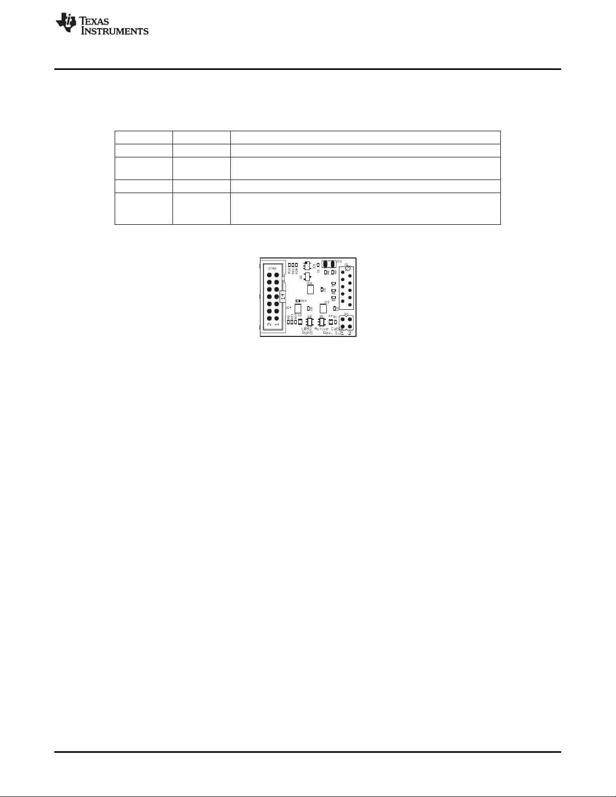
www.ti.com
Figure B-6 shows the PCB layout for the Active Cable. The following pinning is possible:
• JP1 has two jumpers (Jumper 1 and Jumper 2) that can be set as shown in Table B-3.
• JP2 is for reset. For the standard MSP-TS430L092, this jumper must be set. It sets the reset pin to
MSP-TS430L092 Active Cable
Table B-3. MSP-TS430L092 JP1 Settings
Jumper 1 Jumper 2 Description
Off Off The active cable has no power and does not function.
Off On
On Off The active cable receives power from the JTAG connector.
On On this option, the target socket must not have its own power source, as this
The active cable receives power from target socket. For this option, the
target socket must have its own power supply.
The JTAG connector powers the active cable and the target socket. For
would cause a not defined state.
high and can also control it. Without this jumper on the MSP-TS430L092, reset is set to zero.
Figure B-6. MSP-TS430L092 Active Cable Target Socket Module, PCB
SLAU278F–May 2009–Revised December 2010 Hardware
Submit Documentation Feedback
© 2009–2010, Texas Instruments Incorporated
41
Page 42

MSP-TS430L092 Active Cable
Pos. Ref Des Description DigiKey Part No. Comment
C1, C3, C5,
1 4 100nF, SMD0603
2 C2, C4 2 1uF, SMD0805
3 R1, R10 2 10K, SMD0603
4 R2 1 4K7, SMD0603
5 4 100, SMD0603
6 R8 1 680k, SMD0603
7 R11, R15 2 1K, SMD0603
8 R12 0 SMD0603 DNP
9 R13 0 SMD0603 DNP
10 R14 1 0, SMD0603
11 IC1 1 SN74AUC1G04DBVR Manu: TI
12 IC2, IC3, IC4 3 SN74AUC2G125DCTR Manu: TI
13 J2 1 MICRO_STECKV_10 MicroMaTch-Connector: MM
14 JP1 1 2x2 Header JP2Q
15 JP2 1 2-pin header, male, TH SAM1035-02-ND place jumper on header
16 JTAG 1 14-pin connector, male, TH HRP14H-ND
17 Q1 1
18 U1, U2 2 TLVH431IDBVR SOT23-5 Manu: TI
C6
R5, R6, R7,
R9
www.ti.com
Table B-4. MSP-TS430L092 Active Cable Bill of Materials
No. Per
Board
Reichelt:
FL 10G
Put jumper on Position 1 and
2. Do not mix direction.
BC817-25LT1SMD, Digi-Key:
SOT23-BEC BC817-25LT1GOSCT-ND
42
Hardware SLAU278F–May 2009–Revised December 2010
Submit Documentation Feedback
© 2009–2010, Texas Instruments Incorporated
Page 43
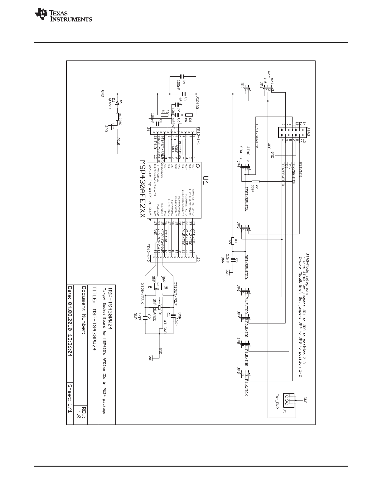
www.ti.com
B.4 MSP-TS430PW24
MSP-TS430PW24
Figure B-7. MSP-TS430PW24 Target Socket Module, Schematic
SLAU278F–May 2009–Revised December 2010 Hardware
Submit Documentation Feedback
© 2009–2010, Texas Instruments Incorporated
43
Page 44

Jumper JP2
Open to measure current
Orient Pin 1 of MSP430 device
D1 LED connected to P1.0
Jumper JP3
Open to disconnect LED
Connector J5
External power connector
Jumper JP1 to "ext"
Jumpers JP4 to JP9
Close 1-2 to debug in Spy-Bi-Wire mode
Close 2-3 to debug in 4-wire JTAG mode
MSP-TS430PW24
www.ti.com
Figure B-8. MSP-TS430PW24 Target Socket Module, PCB
44
Hardware SLAU278F–May 2009–Revised December 2010
Submit Documentation Feedback
© 2009–2010, Texas Instruments Incorporated
Page 45

www.ti.com
MSP-TS430PW24
Table B-5. MSP-TS430PW24 Bill of Materials
Position Ref Des Description DigiKey Part No. Comment
1 C1, C2 0 12pF, SMD0805 DNP
2 C5 1 2.2nF, SMD0805
3 C3, C7 2 10uF/10V, SMD0805
4 C4, C6, C8 3 100nF, SMD0805 478-3351-2-ND
5 D1 1 green LED, SMD0805 P516TR-ND
6 J1, J2 0 12-pin header, TH enclosed with kit. Keep vias free of
J5, JP1,
7 8 3-pin header, male, TH SAM1035-03-ND
8 JP2, JP3 2 2-pin header, male, TH SAM1035-02-ND Place jumper on header
9 9 Jumper 15-38-1024-ND see Pos 7 an 8
10 JTAG 1 HRP14H-ND
11 Q1 0 Crystal DNP: keep vias free of solder
12 R1, R7 2 330 Ω, SMD0805 541-330ATR-ND
13 2 0 Ohm, SMD0805 541-000ATR-ND DNP R5, R6
14 R4 1 47k Ohm, SMD0805 541-47000ATR-ND
15 U1 1 Manuf.: Enplas
16 PCB 1 68.5 x 61 mm 2 layers
17 4 Apply to corners at bottom side
18 MSP430 2 MSP430AFE2xx DNP: enclosed with kit, supplied by TI
JP4, JP5, Place jumper on 1-2 of JP4-JP9
JP6, JP7, Place on 1-2 on JP1
JP8, JP9
R5, R6,
R8, R9,
Adhesive about 6mm width, 2mm e.g., 3M Bumpons Part
plastic feet height No. SJ-5302
No. per
Board
14-pin connector, male,
TH
Socket: OTS
24(28)-065-02-00
"SAM1029-07NDSAM1213-07-ND"
DNP: Headers and receptacles
solder. (Header & Receptacle)
SLAU278F–May 2009–Revised December 2010 Hardware
Submit Documentation Feedback
© 2009–2010, Texas Instruments Incorporated
45
Page 46

MSP-TS430DW28
B.5 MSP-TS430DW28
www.ti.com
46
Figure B-9. MSP-TS430DW28 Target Socket Module, Schematic
Hardware SLAU278F–May 2009–Revised December 2010
Submit Documentation Feedback
© 2009–2010, Texas Instruments Incorporated
Page 47

Jumper J4
Open to disconnect LED
Orient Pin 1 of
MSP430 device
Jumper J5
Open to measure current
Connector J3
External power connector
Remove R8 and jumper R9
LED connected to P1.0
www.ti.com
MSP-TS430DW28
Figure B-10. MSP-TS430DW28 Target Socket Module, PCB
SLAU278F–May 2009–Revised December 2010 Hardware
Submit Documentation Feedback
© 2009–2010, Texas Instruments Incorporated
47
Page 48
MSP-TS430DW28
Position Ref Des Description DigiKey Part No. Comment
1 C1, C2 0 12pF, SMD0805
2 C5 1 100nF, SMD0805
3 C7 1 10uF/10V Tantal Elko B
4 C8 1 10nF SMD0805
5 D1 1 LED3 T1 3mm yellow RS: 228-4991
6 Q1 0 QUARZ, Crystal 32.768kHz, C(Load) = DNP: Cover holes while soldering
7 J1, J2 2 14-pin header, TH male enclosed with kit. Keep vias free of
7.1 2 enclosed with kit. Keep vias free of
8 J3 1 3-Pin Connector, male
9 J4, J5 2 2-Pin Connector, male With jumper
10 BOOTST 0 ML10, 10-Pin Conn., m RS: 482-115 DNP, Cover holes while soldering
11 JTAG 1 ML14, 14-Pin Conn., m RS: 482-121
12 4 0R, SMD0805 DNP: R1, R2, R9, R10
13 R3 1 560R, SMD0805
14 R5 1 47K, SMD0805
15 U1 1 SOP28DW socket
16 U2 0 TSSOP DNP
R1, R2,
R6, R7,
R8,R9,
R10, R11
Table B-6. MSP-TS430DW28 Bill of Materials
No. per
Board
Micro Crystal MS1V-T1K
12.5pF
14-pin header, TH
female
Yamaichi:
IC189-0282-042
www.ti.com
DNP: C1, C2, Cover holes while
soldering
DNP: Headers and receptacles
solder.: Header: Receptacle
DNP: Headers and receptacles
solder.: Header: Receptacle
48
Hardware SLAU278F–May 2009–Revised December 2010
Submit Documentation Feedback
© 2009–2010, Texas Instruments Incorporated
Page 49

www.ti.com
B.6 MSP-TS430PW28
MSP-TS430PW28
Figure B-11. MSP-TS430PW28 Target Socket Module, Schematic
SLAU278F–May 2009–Revised December 2010 Hardware
Submit Documentation Feedback
© 2009–2010, Texas Instruments Incorporated
49
Page 50
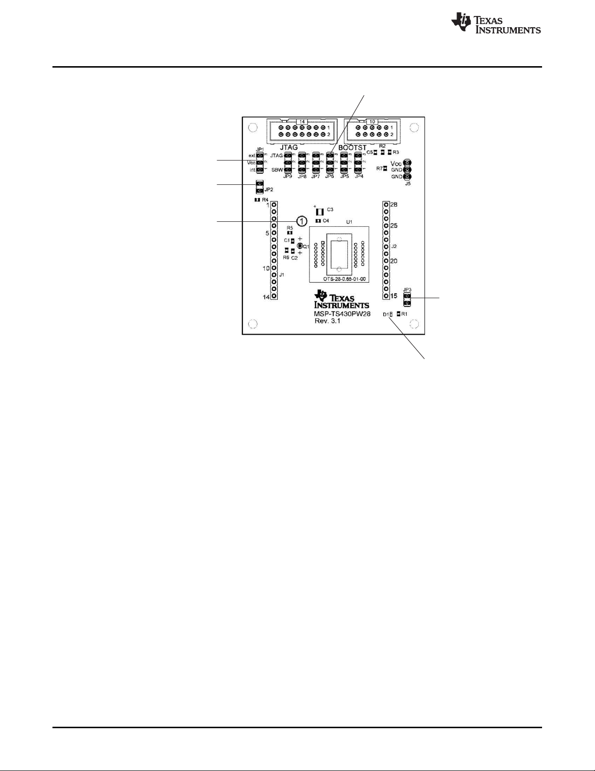
Jumper JP2
Open to measure current
Jumper JP3
Open to disconnect LED
LED D1 connected to P5.1
Jumper JP1
1-2 (int): Power supply via JTAG interface
2-3 (ext): External Power Supply
Jumper JP4 to JP9:
Close 1-2 to debug in Spy-Bi-Wire mode
Close 2-3 to debug in 4-wire JTAG mode
Orient Pin 1 of Device
MSP-TS430PW28
www.ti.com
Figure B-12. MSP-TS430PW28 Target Socket Module, PCB
50
Hardware SLAU278F–May 2009–Revised December 2010
© 2009–2010, Texas Instruments Incorporated
Submit Documentation Feedback
Page 51

www.ti.com
(1)
MSP-TS430PW28
Table B-7. MSP-TS430PW28 Bill of Materials
Pos. Ref Des Description DigiKey Part No. Comment
1 C1, C2 0 12pF, SMD0805
2 C3 1 10uF/10V Tantal Elko B
3 C4 1 100nF, SMD0805
4 C5 0 2.2nF, SMD0805 DNP
5 D1 1 LED green SMD0603
6 Q1 0 QUARZ, Crystal 32.768kHz, C(Load) = neighboring holes while
7 J1, J2 2 14-pin header, TH male kit.Keep vias free of
7.1 2 14-pin header, TH female kit.Keep vias free of
8 J5, IP1 1 3-Pin Connector , male
JP1, JP4,
8a 7 3-Pin Connector , male Jumper on Pos 1-2
JP5, JP6,
JP7, JP8,
JP9
9 JP2, JP3 2 2-Pin Connector , male with Jumper
10 BOOTST 0 ML10, 10-Pin Conn. , m RS: 482-115
11 JTAG 1 ML14, 14-Pin Conn. , m RS: 482-121
12 R1, R7 2 330R, SMD0805
12 0 0R, SMD0805 DNP
R2, R3, R5,
R6
14 R4 1 47K, SMD0805
15 U1 1 SOP28PW socket Enplas: OTS-28-0.65-01
PCB 66 x 79 mm, two layers; Rubber stand off, four pieces
No. per
Board
Micro Crystal MS1V-T1K DNP: Cover holes and
12.5pF soldering
(1)
DNP: C1, C2 , Cover holes
while soldering
DNP: Headers and
receptacles enclosed with
solder.: Header:
Receptacle
DNP: headers and
receptacles enclosed with
solder.: Header:
Receptacle
DNP: Cover holes while
soldering
SLAU278F–May 2009–Revised December 2010 Hardware
Submit Documentation Feedback
© 2009–2010, Texas Instruments Incorporated
51
Page 52

MSP-TS430PW28A
B.7 MSP-TS430PW28A
www.ti.com
52
Figure B-13. MSP-TS430PW28A Target Socket Module, Schematic
Hardware SLAU278F–May 2009–Revised December 2010
Submit Documentation Feedback
© 2009–2010, Texas Instruments Incorporated
Page 53

Jumper JP2
Open to measure current
Orient Pin 1 of MSP430 device
Jumper JP3
Open to disconnect LED
D1 LED connected to P1.0
Connector J5
External power connector
Jumper JP1 to "ext"
Jumpers JP4 to JP9
Close 1-2 to debug in Spy-Bi-Wire mode
Close 2-3 to debug in 4-wire JTAG mode
www.ti.com
MSP-TS430PW28A
Figure B-14. MSP-TS430PW28A Target Socket Module, PCB (Red)
SLAU278F–May 2009–Revised December 2010 Hardware
Submit Documentation Feedback
53
© 2009–2010, Texas Instruments Incorporated
Page 54

MSP-TS430PW28A
Position Ref Des Description DigiKey Part No. Comment
1 C1, C2 0 12pF, SMD0805 DNP
2 C5 1 2.2nF, SMD0805
3 C3 1 10uF/10V, SMD0805
4 C4, C6, 2 100nF, SMD0805 478-3351-2-ND
5 D1 1 green LED, SMD0805 P516TR-ND
6 J1, J2 0 14-pin header, TH enclosed with kit. Keep vias free of
7 8 3-pin header, male, TH SAM1035-03-ND
8 JP2, JP3 2 2-pin header, male, TH SAM1035-02-ND Place jumper on header
9 9 Jumper 15-38-1024-ND see Pos 7 an 8
10 JTAG 1 HRP14H-ND
11 BOOTST 0 DNP Keep vias free of solder
12 Q1 0 Crystal 32.768kHz, C(Load) = DNP: keep vias free of solder
13 R1, R7 2 330 Ω, SMD0805 541-330ATR-ND
14 0 0 Ohm, SMD0805 541-000ATR-ND DNP R2, R3,R5, R6
15 R4 1 47k Ω, SMD0805 541-47000ATR-ND
16 U1 1 Socket: OTS-28-0.65-01 Manuf.: Enplas
17 PCB 1 63.5 x 64.8 mm 2 layers
18 4 Apply to corners at bottom side
19 MSP430 2 MSP430G2553IPW28 DNP: enclosed with kit, supplied by TI
www.ti.com
Table B-8. MSP-TS430PW28A Bill of Materials
No. per
Board
DNP: Headers and receptacles
solder: (Header & Receptacle)
J5, JP1,
JP4, JP5, Place jumper on 1-2 of JP4-JP9
JP6, JP7, Place on 1-2 on JP1
JP8, JP9
14-pin connector, male,
TH
Micro Crystal MS3V
12.5pF
R2, R3,R5,
R6,
Adhesive about 6mm width, 2mm e.g., 3M Bumpons Part
plastic feet height No. SJ-5302
54
Hardware SLAU278F–May 2009–Revised December 2010
Submit Documentation Feedback
© 2009–2010, Texas Instruments Incorporated
Page 55
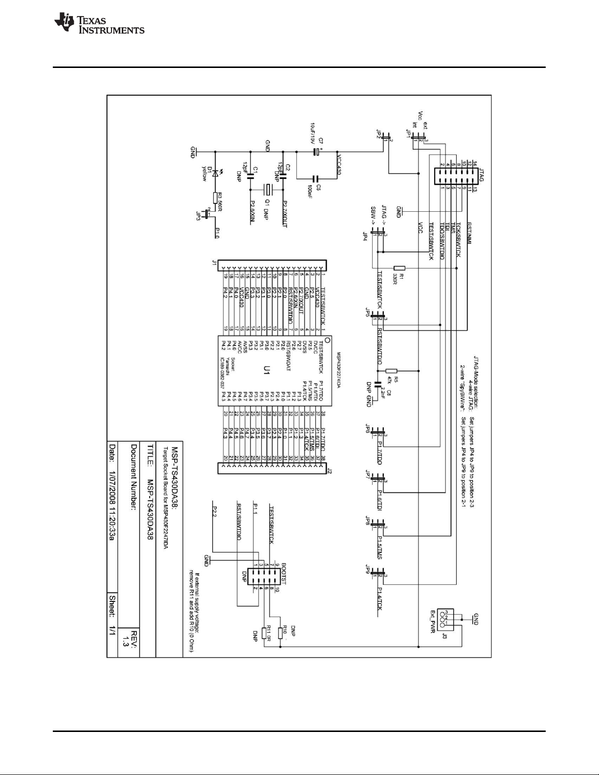
www.ti.com
B.8 MSP-TS430DA38
MSP-TS430DA38
Figure B-15. MSP-TS430DA38 Target Socket Module, Schematic
SLAU278F–May 2009–Revised December 2010 Hardware
Submit Documentation Feedback
© 2009–2010, Texas Instruments Incorporated
55
Page 56

Orient pin 1 of
MSP430 device
LED connected to P1.0
Connector J3
External power connector
Jumper JP1 to 'ext'
Jumper JP3
Open to disconnect LED
Jumper JP2
Open to measure current
Jumpers JP4 to JP9
Close 1-2 to debug in
Spy-Bi-Wire Mode,
Close 2-3 to debug in
4-wire JTAG Mode
MSP-TS430DA38
www.ti.com
Figure B-16. MSP-TS430DA38 Target Socket Module, PCB
56
Hardware SLAU278F–May 2009–Revised December 2010
Submit Documentation Feedback
© 2009–2010, Texas Instruments Incorporated
Page 57

www.ti.com
MSP-TS430DA38
Table B-9. MSP-TS430DA38 Bill of Materials
Pos. Ref Des Description DigiKey Part No. Comment
1 C1, C2 0 12pF, SMD0805 DNP
2 C7 1 10uF/10V, Tantal Size B 511-1463-2-ND
3 C5 1 100nF, SMD0805 478-3351-2-ND
4 C8 0 2.2nF, SMD0805 DNP
5 D1 1 green LED, SMD0603 475-1056-2-ND
6 J1, J2 0 19-pin header, TH kit.Keep vias free of
"J3, JP1,
7 8 3-pin header, male, TH SAM1035-03-ND JP1, JP4,JP5, JP6, JP7,
8 JP2, JP3 2 2-pin header, male, TH SAM1035-02-ND Place jumper on header
9 9 Jumper 15-38-1024-ND
10 JTAG 1 14-pin connector, male, TH HRP14H-ND
11 BOOTST 0 10-pin connector, male, TH
12 Q1 0 Crystal 32.768kHz, C(Load) =
13 R1, R3 2 330 Ω, SMD0805 541-330ATR-ND
14 R10, R11 0 0 Ω, SMD0805 541-000ATR-ND DNP
15 R5 1 47k Ω, SMD0805 541-47000ATR-ND
16 U1 1 Socket: IC189-0382--037 Manuf.: Yamaichi
17 PCB 1 67 x 66 mm 2 layers
18 4 ~6mm width, 2mm height
19 MSP430 2 MSP430F2274IDA
JP4, JP5,
JP6, JP7,
JP8, JP9"
Adhesive e.g., 3M Bumpons Part No. Apply to corners at bottom
Plastic feet SJ-5302 side
No. per
Board
"SAM1029-19NDSAM1213-19-ND"
Micro Crystal MS1V-T1K
12.5pF
DNP: headers and
receptacles enclosed with
solder.: Header:
Receptacle
Place jumpers on headers
JP8, JP9; Pos 1-2
Place on: JP1 - JP9; Pos
1-2
DNP: Keep vias free of
solder
DNP: Keep vias free of
solder
DNP: enclosed with kit
supplied by TI
SLAU278F–May 2009–Revised December 2010 Hardware
Submit Documentation Feedback
© 2009–2010, Texas Instruments Incorporated
57
Page 58
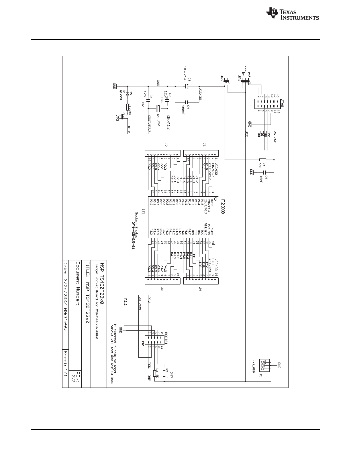
MSP-TS430QFN23x0
B.9 MSP-TS430QFN23x0
www.ti.com
58
Figure B-17. MSP-TS430QFN23x0 Target Socket Module, Schematic
Hardware SLAU278F–May 2009–Revised December 2010
Submit Documentation Feedback
© 2009–2010, Texas Instruments Incorporated
Page 59
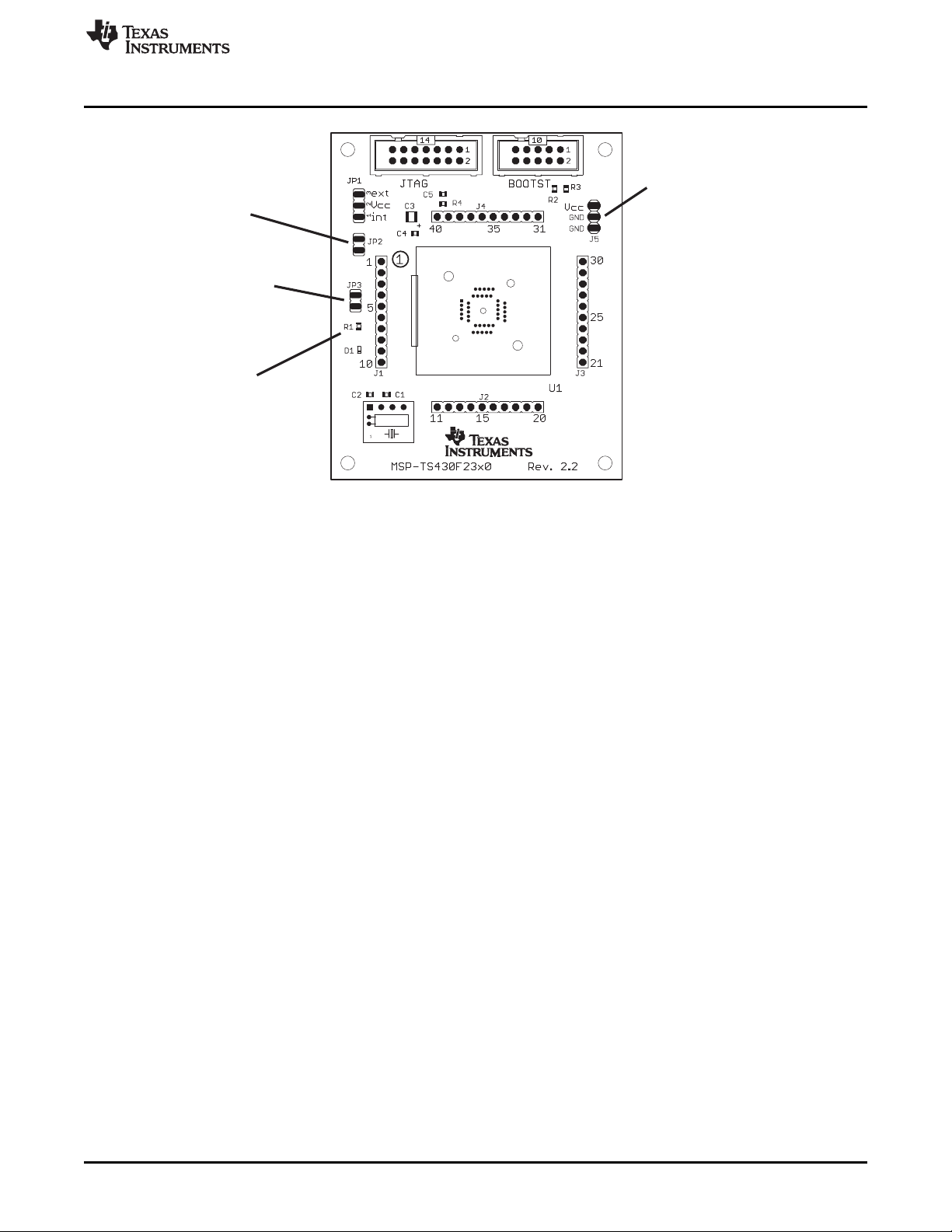
LED connected
to P1.0
Connector J5
External power connector
Jumper JP1 to 'ext'
Jumper JP3
Open to disconnect LED
Jumper JP2
Open to measure current
www.ti.com
MSP-TS430QFN23x0
Figure B-18. MSP-TS430QFN23x0 Target Socket Module, PCB
SLAU278F–May 2009–Revised December 2010 Hardware
Submit Documentation Feedback
59
© 2009–2010, Texas Instruments Incorporated
Page 60

MSP-TS430QFN23x0
Pos. Ref Des Description DigiKey Part No. Comment
1 C1, C2 0 12pF, SMD0805 DNP
2 C3 1 10uF/10V, Tantal Size B 511-1463-2-ND
3 C4 1 100nF, SMD0805 478-3351-2-ND
4 C5 1 10nF, SMD0805 478-1383-2-ND
5 D1 1 green LED, SMD0603 475-1056-2-ND
6 0 10-pin header, TH kit.Keep vias free of
7 J5, JP1 2 3-pin header, male, TH SAM1035-03-ND
8 JP2, JP3 2 2-pin header, male, TH SAM1035-02-ND Place jumper on header
9 3 Jumper 15-38-1024-ND Place on: JP1, JP2, JP3
10 JTAG 1 14-pin connector, male, TH HRP14H-ND
11 BOOTST 0 10-pin connector, male, TH
12 Q1 0 Crystal 32.768kHz, C(Load) =
13 R1 1 330 Ω, SMD0805 541-330ATR-ND
14 R2, R3 0 0 Ω, SMD0805 541-000ATR-ND DNP
15 R4 1 47k Ω, SMD0805 541-47000ATR-ND
16 U1 1 Socket: QFN-40B-0.5-01 Manuf.: Enplas
17 PCB 1 79 x 66 mm 2 layers
18 4 ~6mm width, 2mm height
19 MSP430 2 MSP430F2370IRHA
www.ti.com
Table B-10. MSP-TS430QFN23x0 Bill of Materials
No. per
Board
DNP: headers and
J1, J2, J3, SAM1034-10-NDSAM1212-
J4 10-ND
Micro Crystal MS1V-T1K
12.5pF
Adhesive e.g., 3M Bumpons Part No. Apply to corners at bottom
Plastic feet SJ-5302 side
receptacles enclosed with
solder.: Header:
Receptacle
Place jumper on header
JP1; Pos 1-2.
DNP: Keep vias free of
solder
DNP: Keep vias free of
solder
DNP: enclosed with kit
supplied by TI
60
Hardware SLAU278F–May 2009–Revised December 2010
Submit Documentation Feedback
© 2009–2010, Texas Instruments Incorporated
Page 61
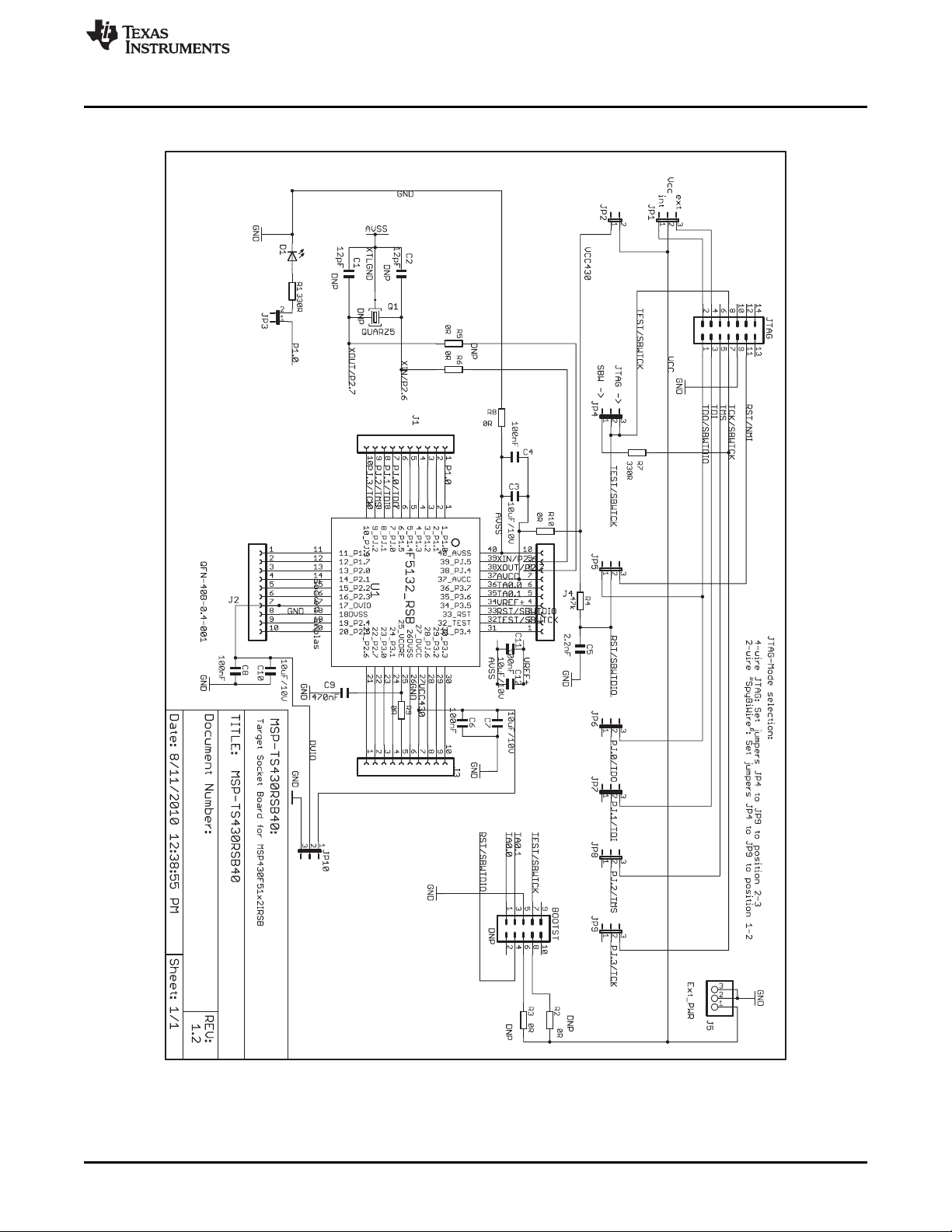
www.ti.com
B.10 MSP-TS430RSB40
MSP-TS430RSB40
Figure B-19. MSP-TS430RSB40 Target Socket Module, Schematic
SLAU278F–May 2009–Revised December 2010 Hardware
Submit Documentation Feedback
© 2009–2010, Texas Instruments Incorporated
61
Page 62
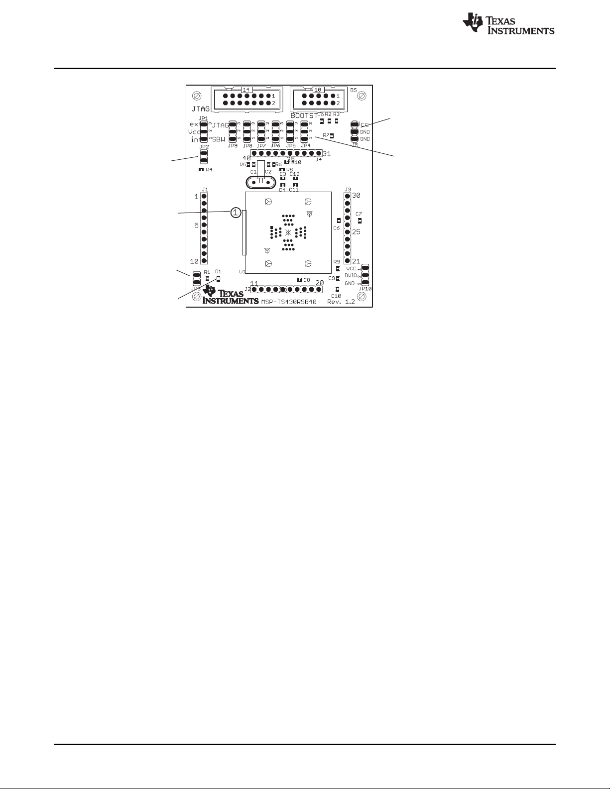
Jumper JP2
Open to measure current
Orient Pin 1 of MSP430 device
Jumper JP3
Open to disconnect LED
D1 LED connected to P1.0
Jumpers JP4 to JP9
Close 1-2 to debug in Spy-Bi-Wire mode
Close 2-3 to debug in 4-wire JTAG mode
Connector J5
External power connector
Jumper JP1 to "ext"
MSP-TS430RSB40
www.ti.com
Figure B-20. MSP-TS430RSB40 Target Socket Module, PCB
62
Hardware SLAU278F–May 2009–Revised December 2010
Submit Documentation Feedback
© 2009–2010, Texas Instruments Incorporated
Page 63
www.ti.com
MSP-TS430RSB40
Table B-11. MSP-TS430RSB40 Bill of Materials
Pos. Ref Des Description DigiKey Part No. Comment
1 C1, C2 0 12pF, SMD0805 DNP: C1, C2
C3, C7, C10,
2 3 10uF/10V, SMD 0805 445-1371-1-ND DNP C12
3 3 100nF, SMD0805 311-1245-2-ND DNP C11
4 C5 1 2.2nF, SMD0805
5 C9 1 470nF, SMD0805
6 D1 1 green LED, SMD0805 P516TR-ND
7 J1, J2, J3, J4 4 10-pin header, TH
7.1 4 10-pin header, TH
8 JP6, JP7, 9 3-pin header, male, TH SAM1035-03-ND
9 JP2, JP3 2 2-pin header, male, TH SAM1035-02-ND place jumper on header
10 JTAG 1 14-pin connector, male, TH HRP14H-ND
11 BOOTST 0 10-pin connector, male, TH
12 U1 1 Enplas
13 Q1 0 Crystal 32.768kHz, C(Load) =
15 10 Jumper 15-38-1024-ND JP4, JP5, JP6, JP7, JP8,
16 R1,R7 2 330R SMD0805
17 R6, R8, R9, 3 0R SMD0805 DNP R2, R3, R5, R6
18 R4 1 47k SMD0805
19 MSP430 2 MSP430F5132
20 4
C12
C4, C6, C8,
C11
JP1,
JP4,JP5,
JP8, JP9, J5,
JP10
R2, R3, R5,
R10
Rubber stand select appropriate; e.g., apply to corners at bottom
off Buerklin: 20H1724 side
No. Per
Board
QFN-40B-0.4_
ENPLAS_SOCKET
Micro Crystal MS3V-T1R
12.5pF
DNP: headers and
receptacles enclosed with kit.
Keep vias free of solder. :
Header : Receptacle
DNP: headers and
receptacles enclosed with kit.
Keep vias free of solder. :
Header : Receptacle
Jumper: 1-2 on JP1, JP10;
2-3 on JP4-JP9
DNP. Keep vias free of
solder
DNP: Q1. Keep vias free of
solder
Place on: JP1, JP2, JP3,
JP9, JP10
DNP: enclosed with kit. Is
supplied by TI
SLAU278F–May 2009–Revised December 2010 Hardware
Submit Documentation Feedback
© 2009–2010, Texas Instruments Incorporated
63
Page 64
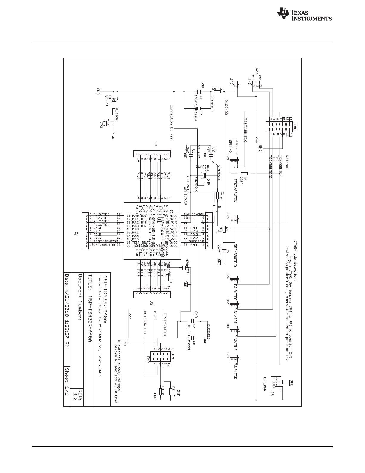
MSP-TS430RHA40A
B.11 MSP-TS430RHA40A
www.ti.com
64
Figure B-21. MSP-TS430RHA40A Target Socket Module, Schematic
Hardware SLAU278F–May 2009–Revised December 2010
Submit Documentation Feedback
© 2009–2010, Texas Instruments Incorporated
Page 65

Jumper JP2
Open to measure current
Connector J5
External power connector
Jumper JP1 to "ext"
Jumpers JP4 to JP9
Close 1-2 to debug in Spy-Bi-Wire mode
Close 2-3 to debug in 4-wire JTAG mode
D1 LED connected to P1.0
Jumper JP3
Open to disconnect LED
Orient Pin 1 of MSP430 device
www.ti.com
MSP-TS430RHA40A
Figure B-22. MSP-TS430RHA40A Target Socket Module, PCB
SLAU278F–May 2009–Revised December 2010 Hardware
Submit Documentation Feedback
© 2009–2010, Texas Instruments Incorporated
65
Page 66
MSP-TS430RHA40A
Position Ref Des Description DigiKey Part No. Comment
1 C1, C2 0 12pF, SMD0805 DNP: C1, C2
2 C5 0 2.2nF, SMD0805 DNP C12
3 C3, C7 2 10uF/10V, SMD0805 5 DNP C11
4 C4, C6 2 100nF, SMD0805 478-3351-2-ND
5 C9 1 470nF, SMD0805
6 D1 1 green LED, SMD0805 P516TR-ND
7 4 10-pin header, TH enclosed with kit. Keep vias free of
7.1 4 10-pin header, TH enclosed with kit. Keep vias free of
8 8 3-pin header, male, TH SAM1035-03-ND
9 JP2, JP3 2 2-pin header, male, TH SAM1035-02-ND place jumper on header
10 9 Jumper 15-38-1024-ND see Pos 8 an 9
11 JTAG 1 HRP14H-ND
12 BOOTST 0 DNP. Keep vias free of solder
13 U1 1 Socket: QFN-40B-0.5-01 Manuf.: Enplas
14 Q1 0 Crystal 32.768kHz, C(Load) = DNP: Q1. Keep vias free of solder
15 R1,R7 2 330R SMD0805 541-330ATR-ND
16 R5, R6, 2 0 Ohm, SMD0805 541-000ATR-ND DNP:R2, R3, R5, R6
17 R4 1 47k SMD0805
18 PCB 1 79 x 66 mm 2 layers
19 4 apply to corners at bottom side
20 MSP430 2 MSP430N5736IRHA
www.ti.com
Table B-12. MSP-TS430RHA40A Bill of Materials
No. per
Board
J1, J2, J3,
J4
J5, JP1,
JP4, JP5, Place jumper on 1-2 of JP4-JP9;
JP6, JP7, Place on 1-2 on JP1
JP8, JP9
14-pin connector, male,
TH
10-pin connector, male,
TH
Micro Crystal MS3V-T1R
12.5pF
R2, R3,
R8, R9,
Rubber select appropriate; e.g.,
stand off Buerklin: 20H1724
DNP: headers and receptacles
solder. : Header : Receptacle
DNP: headers and receptacles
solder. : Header : Receptacle
DNP: enclosed with kit. Is supplied by
TI
66
Hardware SLAU278F–May 2009–Revised December 2010
Submit Documentation Feedback
© 2009–2010, Texas Instruments Incorporated
Page 67
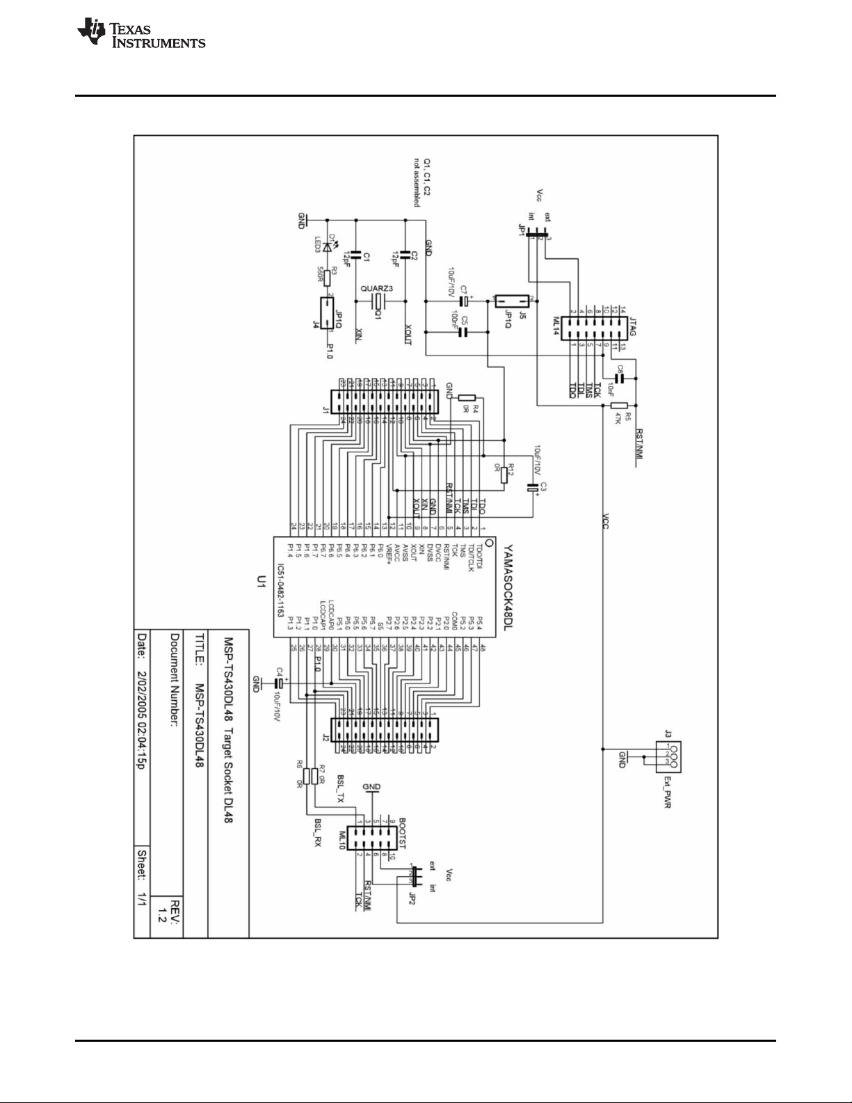
www.ti.com
B.12 MSP-TS430DL48
MSP-TS430DL48
Figure B-23. MSP-TS430DL48 Target Socket Module, Schematic
SLAU278F–May 2009–Revised December 2010 Hardware
Submit Documentation Feedback
© 2009–2010, Texas Instruments Incorporated
67
Page 68

Jumper J4
Open to
disconnect LED
LED connected
to P1.0
Orient pin 1 of
MSP430 device
Jumper J5
Open to measure current
Connector J3
External power connector
Jumper JP1 to ‘ext’
MSP-TS430DL48
www.ti.com
Figure B-24. MSP-TS430DL48 Target Socket Module, PCB
68
Hardware SLAU278F–May 2009–Revised December 2010
© 2009–2010, Texas Instruments Incorporated
Submit Documentation Feedback
Page 69

www.ti.com
MSP-TS430DL48
Table B-13. MSP-TS430DL48 Bill of Materials
Pos. Ref Des Description DigiKey Part No. Comment
1 C1, C2 0 12pF, SMD0805 DNP
2 C4, C7 2 10uF/10V, Tantal Size B 511-1463-2-ND
3 C3, C5 2 100nF, SMD0805 478-3351-2-ND
4 C8 1 10nF, SMD0805 478-1383-2-ND
5 D1 1 yellow LED, TH, 3mm, T1 511-1251-ND
6 J1, J2 0 24-pin header, TH kit.Keep vias free of
7 J3, JP1, JP2 2 3-pin header, male, TH SAM1035-03-ND
8 J4, J5 2 2-pin header, male, TH SAM1035-02-ND Place jumper on header
9 3 Jumper 15-38-1024-ND Place on: JP1, J4, J5
10 JTAG 1 14-pin connector, male, TH HRP14H-ND
11 BOOTST 0 10-pin connector, male, TH
12 Q1 0 Crystal 32.768kHz, C(Load) =
13 R3 1 560 Ω, SMD0805 541-560ATR-ND
14 2 0 Ω, SMD0805 541-000ATR-ND DNP: R6, R7
15 R5 1 47k Ω, SMD0805 541-47000ATR-ND
16 U1 1 Manuf.: Yamaichi
17 PCB 1 58 x 66 mm 2 layers
18 4 ~6mm width, 2mm height
19 MSP430 2 MSP430F4270IDL
R4, R6, R7,
R12
Adhesive e.g., 3M Bumpons Part No. Apply to corners at bottom
Plastic feet SJ-5302 side
No. per
Board
Socket: IC51-1387
KS-15186
SAM1034-12-NDSAM121212-ND
Micro Crystal MS1V-T1K
12.5pF
DNP: Headers and
receptacles enclosed with
solder.: Header:
Receptacle
Place jumper on header
JP1; Pos 1-2. DNP: JP2
DNP: Keep vias free of
solder
DNP: Keep vias free of
solder
DNP: Enclosed with kit
supplied by TI
SLAU278F–May 2009–Revised December 2010 Hardware
Submit Documentation Feedback
© 2009–2010, Texas Instruments Incorporated
69
Page 70

MSP-TS430RGZ48B
B.13 MSP-TS430RGZ48B
www.ti.com
70
Figure B-25. MSP-TS430RGZ48B Target Socket Module, Schematic
Hardware SLAU278F–May 2009–Revised December 2010
Submit Documentation Feedback
© 2009–2010, Texas Instruments Incorporated
Page 71

Jumper JP2
Open to disconnect LED
Connector J5
External power connector
Jumper JP1 to "ext"
Jumpers JP5 to JP10
Close 1-2 to debug in Spy-Bi-Wire mode
Close 2-3 to debug in 4-wire JTAG mode
D1 LED connected to P1.0
Jumper JP1
Open to measure current
Orient Pin 1 of MSP430 device
www.ti.com
MSP-TS430RGZ48B
Figure B-26. MSP-TS430RGZ48B Target Socket Module, PCB
SLAU278F–May 2009–Revised December 2010 Hardware
Submit Documentation Feedback
71
© 2009–2010, Texas Instruments Incorporated
Page 72

MSP-TS430RGZ48B
Position Ref Des Description DigiKey Part No. Comment
1 C1, C2 0 12pF, SMD0805 DNP
2 C3, C4 0 47pF, SMD0805 DNP
3 3 10uF/6.3V, SMD0805
4 4 100nF, SMD0805 311-1245-2-ND
5 C8 1 2.2nF, SMD0805
6 C9 1 470nF, SMD0805 478-1403-2-ND
7 D1 1 green LED, SMD0805 P516TR-ND
8 0 12-pin header, TH enclosed with kit. Keep vias free of
9 J5 1 3-pin header, male, TH
10 7 3-pin header, male, TH SAM1035-03-ND JP6, JP7, JP8, JP9, JP10 place
11 JP1, JP2 2 2-pin header, male, TH SAM1035-02-ND Place jumper on header
12 9 Jumper 15-38-1024-ND See Pos. 10and Pos. 11
13 JTAG 1 HRP14H-ND
14 BOOTST 0 "DNP Keep vias free of solder"
15 Q1 0 Crystal 32.768kHz, C(Load) = DNP: Q1 Keep vias free of solder
16 Q2 0 Crystal DNP: Q2 Keep vias free of solder
17 0 Insulating disk to Q2 t_Detail.cfm?ART_ART
18 R3, R7 2 330 Ω, SMD0805 541-330ATR-ND
19 R8, 3 0 Ohm, SMD0805 541-000ATR-ND DNP: R6, R8, R9, R10, R11,R12
20 R5 1 47k Ω, SMD0805 541-47000ATR-ND
21 U1 1 QFN11T048- Manuf.: Yamaichi
22 PCB 1 81 x 76 mm 2 layers
23 4 Apply to corners at bottom side
24 MSP430 2 MSP430F5342IRGZ DNP: enclosed with kit, supplied by TI
Table B-14. MSP-TS430RGZ48B Bill of Materials
No. per
Board
C6, C7,
C12
C5, C11,
C13, C14
J1, J2, J3, (Header)
J4 SAM1213-12-ND
JP3, JP5,
JP6, JP7,
JP8, JP9,
JP10
14-pin connector, male,
TH
10-pin connector, male,
TH
Insulating
disk to Q2
R1, R2,
R4, R6,
R9,R10,
R11, R12
Socket:
008_A101121_RGZ48
Adhesive about 6mm width, 2mm e.g., 3M Bumpons Part
plastic feet height No. SJ-5302
SAM1029-12-ND
(Receptacle)
Micro Crystal MS3V-T1R
12.5pF
Q2: 4MHz Buerklin:
78D134
http://www.ettinger.de/Ar
NUM=70.08.121
www.ti.com
DNP: Headers and receptacles
solder:
place jumpers on pins 2-3 on JP5,
jumpers on pins 1-2 on JP3,
72
Hardware SLAU278F–May 2009–Revised December 2010
Submit Documentation Feedback
© 2009–2010, Texas Instruments Incorporated
Page 73

www.ti.com
B.14 MSP-TS430PM64
MSP-TS430PM64
NOTE: Connections between the JTAG header and pins XOUT and XIN are no longer required and should not be
made.
Figure B-27. MSP-TS430PM64 Target Socket Module, Schematic
SLAU278F–May 2009–Revised December 2010 Hardware
Submit Documentation Feedback
© 2009–2010, Texas Instruments Incorporated
73
Page 74
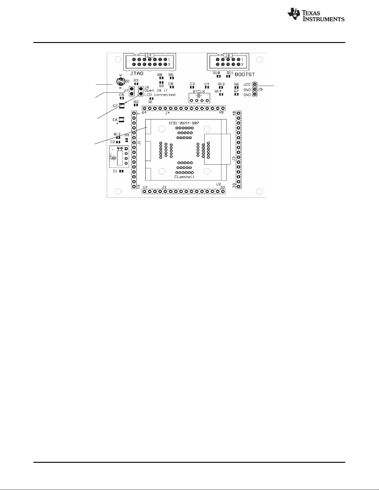
Connector J5
External power connection
Remove R8 and jumper R9
LED connected
to pin 12
Jumper J6
Open to disconnect LED
Jumper J7
Open to measure current
Orient Pin 1 of
MSP430 device
MSP-TS430PM64
www.ti.com
Figure B-28. MSP-TS430PM64 Target Socket Module, PCB
74
Hardware SLAU278F–May 2009–Revised December 2010
Submit Documentation Feedback
© 2009–2010, Texas Instruments Incorporated
Page 75
www.ti.com
MSP-TS430PM64
Table B-15. MSP-TS430PM64 Bill of Materials
Pos. Ref Des Description DigiKey Part No. Comment
1 C1, C2 0 12pF, SMD0805 DNP
1.1 C3, C4 0 47pF, SMD0805 recommendation. Check
2 C6, C7 1 10uF/10V, Tantal Size B 511-1463-2-ND DNP: C6
3 C5 1 100nF, SMD0805 478-3351-2-ND
4 C8 1 10nF, SMD0805 478-1383-2-ND
5 C9 1 470nF, SMD0805 478-1403-2-ND
6 D1 1 green LED, SMD0805 P516TR-ND
7 0 16-pin header, TH kit.Keep vias free of
8 J5 1 3-pin header, male, TH SAM1035-03-ND
9 J6, J7 2 2-pin header, male, TH SAM1035-02-ND Place jumper on header
11 2 Jumper 15-38-1024-ND Place on: J6, J7
12 JTAG 1 14-pin connector, male, TH HRP14H-ND
13 BOOTST 0 10-pin connector, male, TH
14 Q1, Q2 0 Crystal MS1V-T1K 32.768kHz,
15 R3 1 330 Ω, SMD0805 541-330ATR-ND
16 R9, R10, 3 0 Ω, SMD0805 541-000ATR-ND
17 R5 1 47k Ω, SMD0805 541-47000ATR-ND
18 U1 1 Socket: IC51-0644-807 Manuf.: Yamaichi
19 PCB 1 78 x 75 mm 2 layers
20 4 select appropriate
21 MSP430 22
J1, J2, J3, SAM1029-16-NDSAM1213-
J4 16-ND
R1, R2, R4,
R6, R7, R8,
R11, R12,
R13, R14
Rubber Apply to corners at bottom
standoff side
No. per
Board
DNP: Only
your crystal spec.
DNP: Headers and
receptacles enclosed with
solder.: Header:
Receptacle
DNP: Keep vias free of
solder
Q1: Micro Crystal
C(Load) = 12.5pF
MSP430F2619IPM DNP: Enclosed with kit
MSP430F417IPM supplied by TI
DNP: Keep vias free of
solder
DNP: R4, R6, R7, R9, R10,
R11, R12, R13, R14
SLAU278F–May 2009–Revised December 2010 Hardware
Submit Documentation Feedback
© 2009–2010, Texas Instruments Incorporated
75
Page 76

MSP-TS430PM64A
B.15 MSP-TS430PM64A
www.ti.com
76
Figure B-29. MSP-TS430PM64A Target Socket Module, Schematic
Hardware SLAU278F–May 2009–Revised December 2010
Submit Documentation Feedback
© 2009–2010, Texas Instruments Incorporated
Page 77
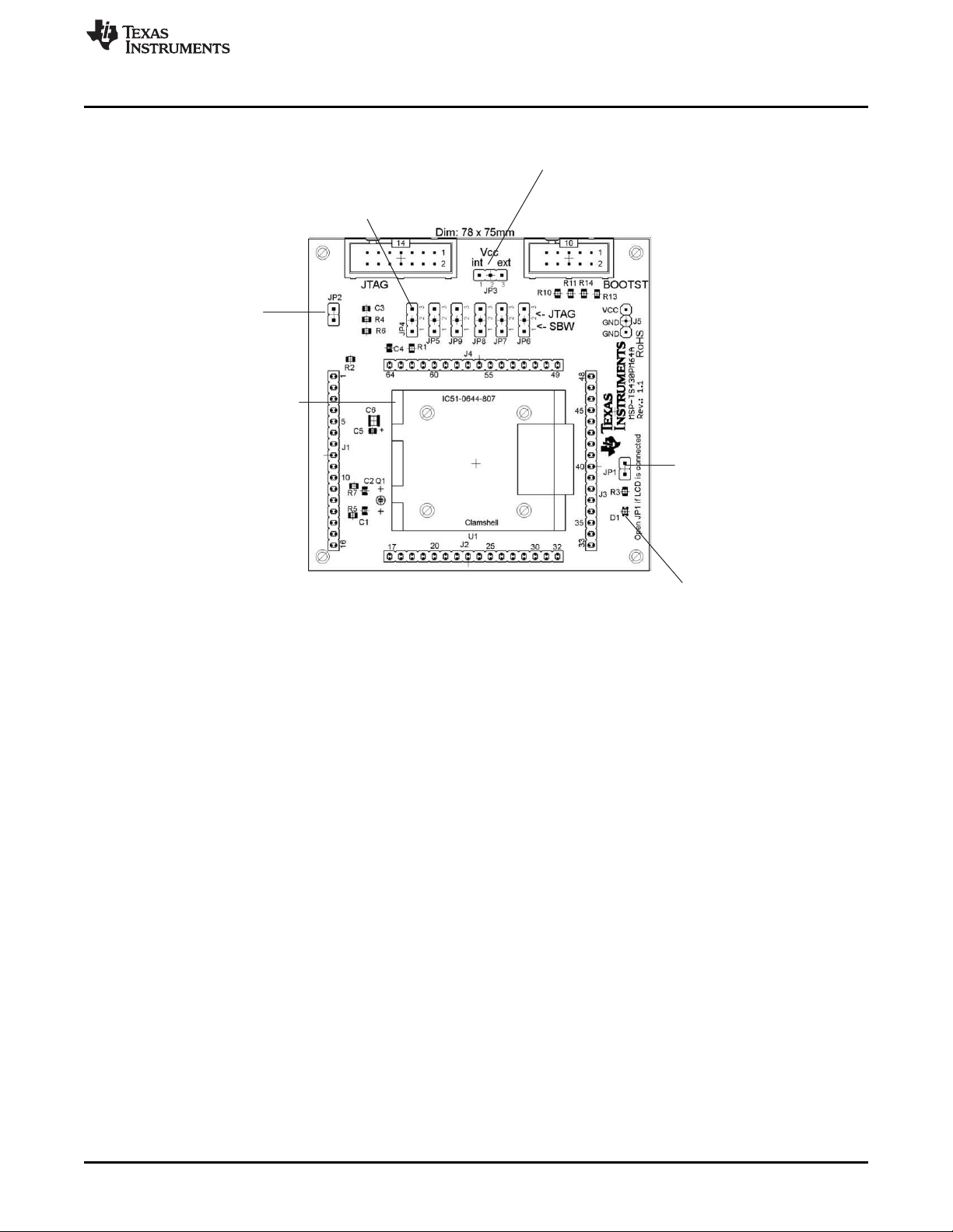
Jumper JP2
Open to measure current
Jumper JP1
Open to disconnect LED
LED D1 connected to P5.1
Jumper JP3
1-2 (int): Power supply via JTAG interface
2-3 (ext): External Power Supply
Jumper JP4 to JP9:
Close 1-2 to debug in Spy-Bi-Wire mode
Close 2-3 to debug in 4-wire JTAG mode
Orient Pin 1 of Device
www.ti.com
MSP-TS430PM64A
Figure B-30. MSP-TS430PM64A Target Socket Module, PCB
SLAU278F–May 2009–Revised December 2010 Hardware
Submit Documentation Feedback
© 2009–2010, Texas Instruments Incorporated
77
Page 78
MSP-TS430PM64A
Pos. Ref Des Description DigiKey Part No. Comment
1 C1, C2, 0 12pF, SMD0805 DNP
2 C3 0 2.2nF, SMD0805 DNP
3 C6, 1 10uF/10V, Tantal Size B 511-1463-2-ND
4 C4, C5 2 100nF, SMD0805 478-3351-2-ND
5 D1 1 green LED, SMD0805 P516TR-ND
6 0 16-pin header, TH kit. Keep vias free of
7 8 3-pin header, male, TH SAM1035-03-ND
8 JP1, JP2 2 2-pin header, male, TH SAM1035-02-ND Place jumper on header
9 2 Jumper 15-38-1024-ND Place on: J6, J7
10 JTAG 1 14-pin connector, male, TH HRP14H-ND
11 BOOTST 0 10-pin connector, male, TH
12 Q1 0 Crystal 32.768kHz, C(Load) =
13 R3, R6 2 330 Ω, SMD0805 541-330ATR-ND
14 2 0 Ω, SMD0805 541-000ATR-ND
15 R4 1 47k Ω, SMD0805 541-47000ATR-ND
16 U1 1 Socket: IC51-0644-807 Manuf.: Yamaichi
17 PCB 1 78 x 75 mm 4 layers
18 4 select appropriate
19 MSP430 2 MSP430F4152IPM
www.ti.com
Table B-16. MSP-TS430PM64A Bill of Materials
No. per
Board
DNP: Headers and
J1, J2, J3, SAM1029-16-NDSAM1213-
J4 16-ND
J5, JP3,
JP4, JP5,
JP6, JP7,
JP8, JP9
Micro Crystal MS1V-T1K
12.5pF
R1, R2, R5,
R7, R9, R10, DNP: R5, R7, R9, R10,
R11, R13, R11, R13, R14
R14
Rubber Apply to corners at bottom
stand off side
receptacles enclosed with
solder.: Header:
Receptacle
DNP: Keep vias free of
solder
DNP: Keep vias free of
solder
DNP: Enclosed with kit
supplied by TI
78
Hardware SLAU278F–May 2009–Revised December 2010
Submit Documentation Feedback
© 2009–2010, Texas Instruments Incorporated
Page 79
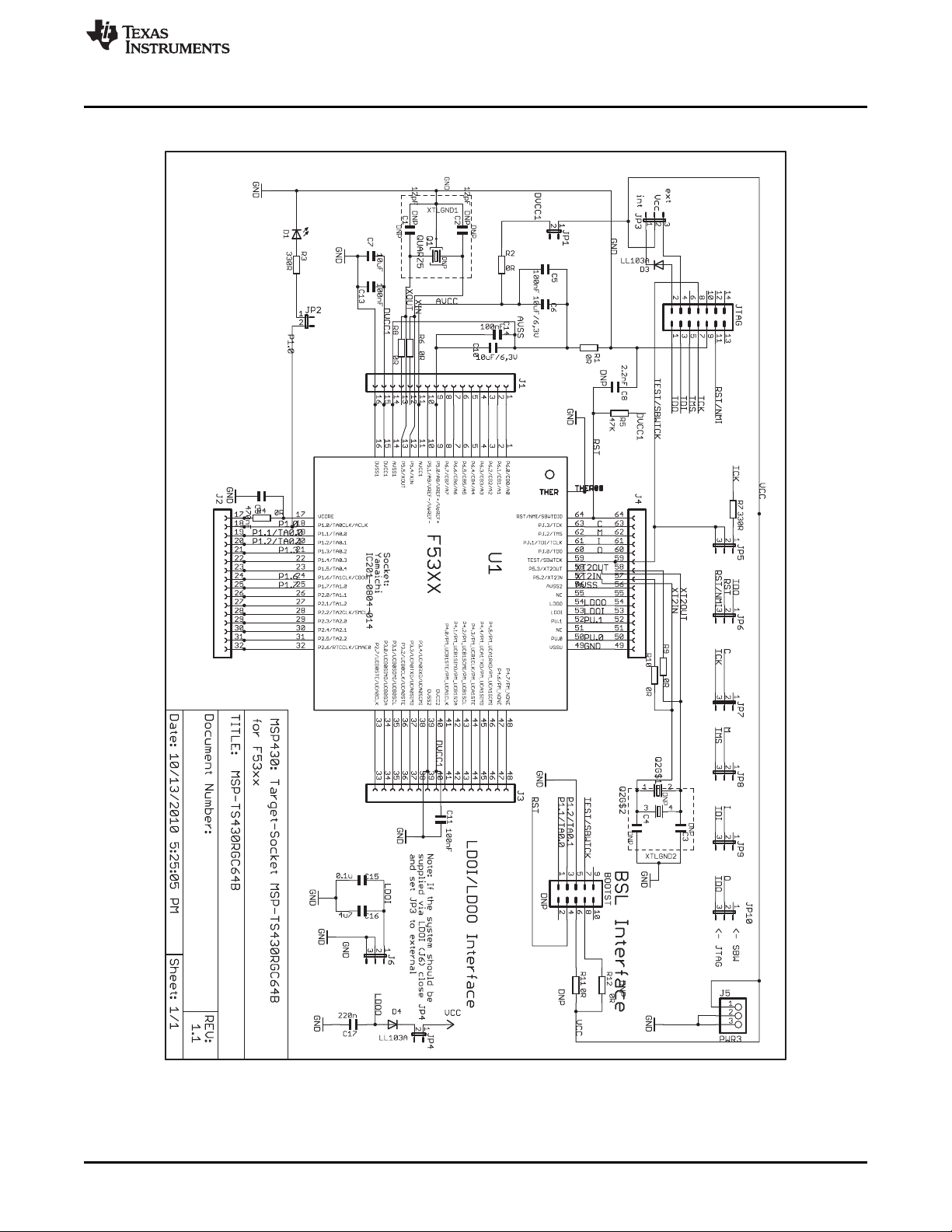
www.ti.com
B.16 MSP-TS430RGC64B
MSP-TS430RGC64B
Figure B-31. MSP-TS430RGC64B Target Socket Module, Schematic
SLAU278F–May 2009–Revised December 2010 Hardware
Submit Documentation Feedback
© 2009–2010, Texas Instruments Incorporated
79
Page 80

Jumper JP2
Open to disconnect LED
Connector J5
External power connector
Jumper JP3 to "ext"
Jumpers JP5 to JP10
Close 1-2 to debug in Spy-Bi-Wire mode
Close 2-3 to debug in 4-wire JTAG mode
D1 LED connected to P1.0
If the system should
be supplied via LDOI (J6),
close JP4 and
set JP3 to external
Orient Pin 1 of MSP430 device
MSP-TS430RGC64B
www.ti.com
Figure B-32. MSP-TS430RGC64B Target Socket Module, PCB
80
Hardware SLAU278F–May 2009–Revised December 2010
© 2009–2010, Texas Instruments Incorporated
Submit Documentation Feedback
Page 81
www.ti.com
MSP-TS430RGC64B
Table B-17. MSP-TS430RGC64B Bill of Materials
Position Ref Des Description DigiKey Part No. Comment
1 C1, C2 0 12pF, SMD0805 DNP
2 C3, C4 0 47pF, SMD0805 DNP
3 3 10uF/6.3V, SMD0805
4 C13, C14, 5 100nF, SMD0805 311-1245-2-ND
5 C8 1 2.2nF, SMD0805
6 C9 1 470nF, SMD0805 478-1403-2-ND
7 C16 1 4.7uF, SMD0805
8 C17 1 220nF, SMD0805
9 D1 1 green LED, SMD0805 P516TR-ND
10 0 16-pin header, TH enclosed with kit. Keep vias free of
11 J5 , J6 2 3-pin header, male, TH
12 7 3-pin header, male, TH SAM1035-03-ND JP6, JP7, JP8, JP9, JP10 place
13 3 2-pin header, male, TH SAM1035-02-ND Place jumper on header
14 10 Jumper 15-38-1024-ND See Pos. 12 and Pos. 13
15 JTAG 1 HRP14H-ND
16 BOOTST 0 "DNP Keep vias free of solder"
17 Q1 0 Crystal 32.768kHz, C(Load) = DNP: Q1 Keep vias free of solder
18 Q2 0 Crystal DNP: Q2 Keep vias free of solder
19 0 Insulating disk to Q2 t_Detail.cfm?ART_ART
20 R3, R7 2 330 Ω, SMD0805 541-330ATR-ND
21 R8, 3 0 Ohm, SMD0805 541-000ATR-ND DNP: R6, R8, R9, R10, R11,R12
22 R5 1 47k Ω, SMD0805 541-47000ATR-ND
23 U1 1 Manuf.: Yamaichi
24 PCB 1 85 x 76 mm 2 layers
25 4 Apply to corners at bottom side
26 D3,D4
27 MSP430 2 MSP430F5310 RGC DNP: enclosed with kit, supplied by TI
C6, C7,
C10
C5, C11,
C15
J1, J2, J3, (Header)
J4 SAM1213-16-ND
JP3, JP5,
JP6, JP7,
JP8, JP9,
JP10
JP1, JP2,
JP4
Insulating
disk to Q2
R1, R2,
R4, R6,
R9,R10,
R11, R12
Adhesive about 6mm width, 2mm e.g., 3M Bumpons Part
plastic feet height No. SJ-5302
No. per
Board
14-pin connector, male,
TH
10-pin connector, male,
TH
Socket:
QFN11T064-006-N-HSP
SAM1029-16-ND
(Receptacle)
Micro Crystal MS3V-T1R
12.5pF
Q2: 4MHz Buerklin:
78D134
http://www.ettinger.de/Ar
NUM=70.08.121
DNP: Headers and receptacles
solder:
place jumpers on pins 2-3 on JP5,
jumpers on pins 1-2 on JP3,
SLAU278F–May 2009–Revised December 2010 Hardware
Submit Documentation Feedback
© 2009–2010, Texas Instruments Incorporated
81
Page 82

MSP-TS430RGC64USB
B.17 MSP-TS430RGC64USB
Due to the use of diodes in the power chain, the voltage on the MSP430F5xx device is approximately
0.3 V lower than is set by the debugging tool. Set the voltage in the IDE to 0.3 V higher than desired; for
example, to run the MCU at 3.0 V, set it to 3.3 V.
www.ti.com
82
Figure B-33. MSP-TS430RGC64USB Target Socket Module, Schematic
Hardware SLAU278F–May 2009–Revised December 2010
Submit Documentation Feedback
© 2009–2010, Texas Instruments Incorporated
Page 83

www.ti.com
MSP-TS430RGC64USB
Figure B-34. MSP-TS430RGC64USB Target Socket Module, PCB
SLAU278F–May 2009–Revised December 2010 Hardware
Submit Documentation Feedback
© 2009–2010, Texas Instruments Incorporated
83
Page 84

MSP-TS430RGC64USB
Pos. Ref Des Description DigiKey Part No. Comment
1 C1, C2 0 12pF, SMD0805 DNP: C1, C2
1.1 C3, C4 2 47pF, SMD0805
2 C6, C7 2 10uF/6.3V, Tantal Size B 511-1463-2-ND
C5, C11,
3 4 100nF, SMD0805 311-1245-2-ND
C13, C14
3.1 C10, C12 0 10uF, SMD0805 DNP: C10, C12
4 C8 1 2.2nF, SMD0805
5 C9 1 470nF, SMD0805 478-1403-2-ND
6 D1 1 green LED, SMD0805 P516TR-ND
7 J1, J2, J3, J4 4 16-pin header, TH
8 J5 1 3-pin header, male, TH SAM1035-03-ND
JP5, JP6,
9 JP7, JP8, 6 3-pin header, male, TH SAM1035-03-ND place jumpers on pins 2-3
JP9, JP10
JP1, JP2,
10 3 2-pin header, male, TH SAM1035-02-ND place jumper on header
11 JP3 1 3-pin header, male, TH SAM1035-03-ND place jumper on pins 1-2
12 10 Jumper 15-38-1024-ND JP4, JP5, JP6, JP7, JP8,
13 JTAG 1 14-pin connector, male, TH HRP14H-ND
14 Q1 0 Crystal 32.768kHz, C(Load) =
15 Q2 1 Crystal Q2: 4MHz Buerklin: 78D134
16 R3, R7 2 330 Ω, SMD0805 541-330ATR-ND
17 R6, R8, R9, 2 0 Ω, SMD0805 541-000ATR-ND DNP: R4, R6, R8, R9, R12
18 R10 1 100 Ω, SMD0805 Buerklin: 07E500
18 R11 1 1M Ω, SMD0805
18 R5 1 47k Ω, SMD0805 541-47000ATR-ND
19 U1 1 Socket: QFN11T064-006 Manuf.: Yamaichi
20 PCB 1 79 x 77 mm 2 layers
21 4 Buerklin: 20H1724
22 MSP430 2 MSP430F5509 RGC
23 1 Insulating disk to Q2 tail.cfm?ART_ARTNUM=70.0
27 C33 1 220n SMD0603 Buerklin: 53D2074
28 C35 1 10p SMD0603 Buerklin: 56D102
29 C36 1 10p SMD0603 Buerklin: 56D102
30 C38 1 220n SMD0603 Buerklin: 53D2074
31 C39 1 4u7 SMD0603 Buerklin: 53D2086
32 C40 1 0.1u SMD0603 Buerklin: 53D2068
33 D2, D3, D4 3 LL103A Buerklin: 24S3406
JP4
R1, R2, R4,
R12
Rubber stand apply to corners at bottom
off side
Insulating
disk to Q2
Table B-18. MSP-TS430RGC64USB Bill of Materials
No. Per
Board
SAM1029-16-ND : Header
SAM1213-16-ND : Receptacle
Q1: Micro Crystal MS1V-T1K
12.5pF
http://www.ettinger.de/Art_De
8.121
www.ti.com
DNP: headers and
receptacles enclosed with kit.
Keep vias free of solder.
Place on: JP1, JP2, JP3,
JP9, JP10
DNP: Q1
Keep vias free of solder"
DNP: enclosed with kit. Is
supplied by TI
84
Hardware SLAU278F–May 2009–Revised December 2010
© 2009–2010, Texas Instruments Incorporated
Submit Documentation Feedback
Page 85

www.ti.com
MSP-TS430RGC64USB
Table B-18. MSP-TS430RGC64USB Bill of Materials (continued)
Pos. Ref Des Description DigiKey Part No. Comment
34 IC7 1 TPD4E004 Manu: TI
36 LED 0 JP3QE SAM1032-03-ND DNP
37 LED1 0 LEDCHIPLED_0603 FARNELL: 852-9833 DNP
38 LED2 0 LEDCHIPLED_0603 FARNELL: 852-9868 DNP
39 LED3 0 LEDCHIPLED_0603 FARNELL: 852-9841 DNP
R13, R15,
40 0 470R Buerklin: 07E564 DNP
41 R33 1 1k4 / 1k5 Buerklin: 07E612
42 R34 1 27R Buerklin: 07E444
43 R35 1 27R Buerklin: 07E444
44 R36 1 33k Buerklin: 07E740
45 S1 0 PB P12225STB-ND DNP
46 S2 0 PB P12225STB-ND DNP
46 S3 1 PB P12225STB-ND
47 USB1 1 USB_RECEPTACLE FARNELL: 117-7885
R16
No. Per
Board
SLAU278F–May 2009–Revised December 2010 Hardware
Submit Documentation Feedback
© 2009–2010, Texas Instruments Incorporated
85
Page 86

MSP-TS430PN80
B.18 MSP-TS430PN80
www.ti.com
86
NOTE: For MSP430F(G)47x devices:
Connect pins 7 and 10 (GND) externally to DVSS(see data sheet).
Connect load capacitance on V
pin 60 when SD16 is used (see data sheet).
ref
Figure B-35. MSP-TS430PN80 Target Socket Module, Schematic
Hardware SLAU278F–May 2009–Revised December 2010
© 2009–2010, Texas Instruments Incorporated
Submit Documentation Feedback
Page 87

Connector J5
External power connection
Remove R8 and jumper R9
LED connected to pin 12
Jumper J6
Open to disconnect LED
Orient Pin 1 of MSP430 device
www.ti.com
MSP-TS430PN80
Figure B-36. MSP-TS430PN80 Target Socket Module, PCB
SLAU278F–May 2009–Revised December 2010 Hardware
Submit Documentation Feedback
87
© 2009–2010, Texas Instruments Incorporated
Page 88

MSP-TS430PN80
Pos. Ref Des Description DigiKey Part No. Comment
1 C1, C2 0 12pF, SMD0805 DNP: C1, C2
1.1 C3, C4 0 47pF, SMD0805 recommendation. Check
2 C6, C7 1 10uF/10V, Tantal Size B 511-1463-2-ND
3 C5 1 100nF, SMD0805 478-3351-2-ND
4 C8 1 10nF, SMD0805 478-1383-2-ND
5 D1 1 green LED, SMD0603 475-1056-2-ND
6 0 25-pin header, TH kit.Keep vias free of
7 J5, JP1 2 3-pin header, male, TH SAM1035-03-ND
8 J6, JP2 2 2-pin header, male, TH SAM1035-02-ND Place jumper on header
9 3 Jumper 15-38-1024-ND
10 JTAG 1 14-pin connector, male, TH HRP14H-ND
11 BOOTST 0 10-pin connector, male, TH
12 Q1, Q2 0 Crystal MS1V-T1K 32.768kHz,
13 R3 1 560 Ω, SMD0805 541-560ATR-ND
14 R6, R7, R10, 2 0 Ω, SMD0805 541-000ATR-ND
15 R5 1 47k Ω, SMD0805 541-47000ATR-ND
16 U1 1 Socket: IC201-0804-014 Manuf.: Yamaichi
17 PCB 1 77 x 77 mm 2 layers
18 4 ~6mm width, 2mm height
19 MSP430 2 MSP430FG439IPN
www.ti.com
Table B-19. MSP-TS430PN80 Bill of Materials
No. per
Board
DNP: Only
your crystal spec.
DNP: Headers and
J1, J2, J3, SAM1029-20-NDSAM1213-
J4 20-ND
Q1: Micro Crystal
C(Load) = 12.5pF
R1, R2, R4,
R11, R12
Adhesive e.g., 3M Bumpons Part No. Apply to corners at bottom
Plastic feet SJ-5302 side
receptacles enclosed with
solder.: Header:
Receptacle
Place on: J6, JP2,
JP1/Pos1-2
DNP: Keep vias free of
solder
DNP: Keep vias free of
solder
DNP: R4, R6, R7, R10,
R11, R12
DNP: Enclosed with kit
supplied by TI
88
Hardware SLAU278F–May 2009–Revised December 2010
Submit Documentation Feedback
© 2009–2010, Texas Instruments Incorporated
Page 89

www.ti.com
B.19 MSP-TS430PN80A
MSP-TS430PN80A
Figure B-37. MSP-TS430PN80A Target Socket Module, Schematic
SLAU278F–May 2009–Revised December 2010 Hardware
Submit Documentation Feedback
© 2009–2010, Texas Instruments Incorporated
89
Page 90
Connector J5
External power connector
Jumper JP3 to "ext"
Orient Pin 1 of MSP430 device
Jumpers JP5 to JP10
Close 1-2 to debug in Spy-Bi-Wire mode
Close 2-3 to debug in 4-wire JTAG mode
D1 LED connected to P1.0
Jumper JP2
Open to disconnect LED
If the system should
be supplied via LDOI (J6),
close JP4 and
set JP3 to external
MSP-TS430PN80A
www.ti.com
Figure B-38. MSP-TS430PN80A Target Socket Module, PCB
90
Hardware SLAU278F–May 2009–Revised December 2010
© 2009–2010, Texas Instruments Incorporated
Submit Documentation Feedback
Page 91
www.ti.com
MSP-TS430PN80USB
Table B-20. MSP-TS430PN80A Bill of Materials
Position Ref Des Description DigiKey Part No. Comment
1 C1, C2 0 12pF, SMD0805 DNP
2 C3, C4 0 47pF, SMD0805 DNP
3 3 10uF/6.3V, SMD0805 DNP C10
4 C13, C14, 5 100nF, SMD0805 311-1245-2-ND
5 C8 1 2.2nF, SMD0805
6 C9 1 470nF, SMD0805 478-1403-2-ND
7 C16 1 4.7uF, SMD0805
8 C17 1 220nF, SMD0805
9 D1 1 green LED, SMD0805 P516TR-ND
10 0 20-pin header, TH enclosed with kit. Keep vias free of
11 J5 , J6 2 3-pin header, male, TH
12 7 3-pin header, male, TH SAM1035-03-ND JP6, JP7, JP8, JP9, JP10 place
13 3 2-pin header, male, TH SAM1035-02-ND Place jumper on header
14 10 Jumper 15-38-1024-ND See Pos. 12 and Pos. 13
15 JTAG 1 HRP14H-ND
16 BOOTST 0 "DNP Keep vias free of solder"
17 Q1 0 Crystal 32.768kHz, C(Load) = DNP: Q1 Keep vias free of solder
18 Q2 0 Crystal DNP: Q2 Keep vias free of solder
19 0 Insulating disk to Q2 t_Detail.cfm?ART_ART
20 D3,D4 2 LL103A Buerklin: 24S3406
21 R3, R7 2 330 Ω, SMD0805 541-330ATR-ND
22 R8, 3 0 Ohm, SMD0805 541-000ATR-ND DNP: R6, R8, R9, R10, R11,R12
23 R5 1 47k Ω, SMD0805 541-47000ATR-ND
24 U1 1 Socket:IC201-0804-014 Manuf.: Yamaichi
25 PCB 1 77 x 91 mm 2 layers
26 4 Apply to corners at bottom side
27 MSP430 2 MSP430F5329IPN DNP: enclosed with kit, supplied by TI
C6, C7,
C10, C12
C5, C11,
C15
J1, J2, J3, (Header)
J4 SAM1213-20-ND
JP3, JP5,
JP6, JP7,
JP8, JP9,
JP10
JP1, JP2,
JP4
Insulating
disk to Q2
R1, R2,
R4, R6,
R9,R10,
R11, R12
Adhesive about 6mm width, 2mm e.g., 3M Bumpons Part
plastic feet height No. SJ-5302
No. per
Board
14-pin connector, male,
TH
10-pin connector, male,
TH
SAM1029-20-ND
(Receptacle)
Micro Crystal MS3V-T1R
12.5pF
Q2: 4MHz Buerklin:
78D134
http://www.ettinger.de/Ar
NUM=70.08.121
DNP: Headers and receptacles
solder:
place jumpers on pins 2-3 on JP5,
jumpers on pins 1-2 on JP3,
B.20 MSP-TS430PN80USB
Due to the use of diodes in the power chain, the voltage on the MSP430F5xx device is approximately
0.3 V lower than is set by the debugging tool. Set the voltage in the IDE to 0.3 V higher than desired; for
example, to run the MCU at 3.0 V, set it to 3.3 V.
SLAU278F–May 2009–Revised December 2010 Hardware
Submit Documentation Feedback
© 2009–2010, Texas Instruments Incorporated
91
Page 92

MSP-TS430PN80USB
www.ti.com
92
NOTE: R11 should be populated.
Figure B-39. MSP-TS430PN80USB Target Socket Module, Schematic
Hardware SLAU278F–May 2009–Revised December 2010
Submit Documentation Feedback
© 2009–2010, Texas Instruments Incorporated
Page 93
Jumper JP3
1-2 (int): Power supply via JTAG debug interface
2-3 (ext): External power supply
Connector J5
External power connector
Jumper JP3 to ‘ext’
USB Connector
BSL invoke button S3
Jumper JP4
Close for USB bus powered
device
Jumper JP2
Open to disconnect LED
LED connected to P1.0
Jumper JP1
Open to measure current
Jumper JP5 to JP10
Close 1-2 to debug in Spy-Bi-
Wire mode.
Close 2-3 to debug in 4-wire
JTAG mode.
www.ti.com
MSP-TS430PN80USB
Figure B-40. MSP-TS430PN80USB Target Socket Module, PCB
SLAU278F–May 2009–Revised December 2010 Hardware
Submit Documentation Feedback
93
© 2009–2010, Texas Instruments Incorporated
Page 94
MSP-TS430PN80USB
Pos. Ref Des Description DigiKey Part No. Comment
1 C1, C2 0 12pF, SMD0805 DNP: C1, C2
1.1 C3, C4 2 47pF, SMD0805
2 C6, C7 2 10uF/6.3V, Tantal Size B 511-1463-2-ND
3 4 100nF, SMD0805 311-1245-2-ND
3.1 C10, C12 0 10uF, SMD0805 311-1245-2-ND DNP: C10, C12
4 C8 1 2.2nF, SMD0805
5 C9 1 470nF, SMD0805 478-1403-2-ND
6 D1 1 green LED, SMD0805 P516TR-ND
7 4 20-pin header, TH SAM1029-20-ND kit. Keep vias free of
7.1 4 20-pin header, TH SAM1213-20-ND kit. Keep vias free of
8 J5 1 3-pin header, male, TH SAM1035-03-ND
9 6 3-pin header, male, TH SAM1035-03-ND Place jumpers on pins 2-3
10 JP1, JP2 2 2-pin header, male, TH SAM1035-02-ND Place jumper on header
11 JP3 1 3-pin header, male, TH SAM1035-03-ND Place jumper on pins 1-2
12 10 Jumper 15-38-1024-ND JP4, JP5, JP6, JP7, JP8,
13 JTAG 1 14-pin connector, male, TH HRP14H-ND
14 Q1 0 Crystal 32.768kHz, C(Load) =
15 Q2 1 Crystal
16 R3, R7 2 330 Ω, SMD0805 541-330ATR-ND
17 R6, R8, R9, 2 0 Ω, SMD0805 541-000ATR-ND DNP: R4, R6, R8, R9, R12
18 R10 1 100 Ω, SMD0805 Buerklin: 07E500
18 R11 0 1M Ω, SMD0805 DNP
18 R5 1 47k Ω, SMD0805 541-47000ATR-ND
19 U1 1 Socket:IC201-0804-014 Manuf.: Yamaichi
20 PCB 1 79 x 77 mm 2 layers
21 4 Buerklin: 20H1724
22 MSP430 2 MSP430F5529
23 1 Insulating disk to Q2 Detail.cfm?ART_ARTNUM
27 C33 1 220n Buerklin: 53D2074
28 C35 1 10p Buerklin: 56D102
www.ti.com
Table B-21. MSP-TS430PN80USB Bill of Materials
No. per
Board
C5, C11,
C13, C14
DNP: headers and
J1, J2, J3,
J4
JP5, JP6,
JP7,
JP8,JP9,
JP10
JP4 1 SAM1035-02-ND
Micro Crystal MS1V-T1K
12.5pF
"Q2: 4MHzBuerklin:
78D134"
R1, R2, R4,
R12
Rubber Apply to corners at bottom
standoff side
Insulating
disk to Q2
http://www.ettinger.de/Art_
=70.08.121
receptacles enclosed with
solder.: Header:
Receptacle
DNP: headers and
receptacles enclosed with
solder.: Header:
Receptacle
Place jumper only on one
pin
Place on: JP1, JP2, JP3,
JP9, JP10
DNP: Q1 Keep vias free of
solder
DNP: Enclosed with kit
supplied by TI
94
Hardware SLAU278F–May 2009–Revised December 2010
© 2009–2010, Texas Instruments Incorporated
Submit Documentation Feedback
Page 95
www.ti.com
MSP-TS430PN80USB
Table B-21. MSP-TS430PN80USB Bill of Materials (continued)
Pos. Ref Des Description DigiKey Part No. Comment
29 C36 1 10p Buerklin: 56D102
30 C38 1 220n Buerklin: 53D2074
31 C39 1 4u7 Buerklin: 53D2086
32 C40 1 0.1u Buerklin: 53D2068
33 D2, D3, D4 3 LL103A Buerklin: 24S3406
34 IC7 1 TPD4E004 Manu: TI
36 LED 0 JP3QE SAM1032-03-ND DNP
37 LED1 0 LEDCHIPLED_0603 FARNELL: 852-9833 DNP
38 LED2 0 LEDCHIPLED_0603 FARNELL: 852-9868 DNP
39 LED3 0 LEDCHIPLED_0603 FARNELL: 852-9841 DNP
40 0 470R Buerklin: 07E564 DNP
41 R33 1 1k4 Buerklin: 07E612
42 R34 1 27R Buerklin: 07E444
43 R35 1 27R Buerklin: 07E444
44 R36 1 33k Buerklin: 07E740
45 S1 0 PB P12225STB-ND DNP
46 S2 0 PB P12225STB-ND DNP
46 S3 1 PB P12225STB-ND
47 USB1 1 USB_RECEPTACLE FARNELL: 117-7885
R13, R15,
R16
No. per
Board
SLAU278F–May 2009–Revised December 2010 Hardware
Submit Documentation Feedback
© 2009–2010, Texas Instruments Incorporated
95
Page 96

MSP-TS430PZ100
B.21 MSP-TS430PZ100
www.ti.com
96
NOTE: Connections between the JTAG header and pins XOUT and XIN are no longer required and should not be
made.
Figure B-41. MSP-TS430PZ100 Target Socket Module, Schematic
Hardware SLAU278F–May 2009–Revised December 2010
Submit Documentation Feedback
© 2009–2010, Texas Instruments Incorporated
Page 97

Connector J5
External power connection
Remove R8 and jumper R9
LED connected to pin 12
Jumper J6
Open to disconnect LED
Orient Pin 1 of MSP430 device
Jumper J7
Open to measure current
www.ti.com
MSP-TS430PZ100
Figure B-42. MSP-TS430PZ100 Target Socket Module, PCB
SLAU278F–May 2009–Revised December 2010 Hardware
Submit Documentation Feedback
97
© 2009–2010, Texas Instruments Incorporated
Page 98

MSP-TS430PZ100
Pos. Ref Des Description DigiKey Part No. Comment
1 C1, C2, 0 12pF, SMD0805 DNP
1b C3, C4 0 47pF, SMD0805 recommendation. Check
2 C6, C7 1 10uF/10V, Tantal Size B 511-1463-2-ND DNP: C6
3 C5 1 100nF, SMD0805 478-3351-2-ND
4 C8 1 10nF, SMD0805 478-1383-2-ND
5 C9 1 470nF, SMD0805 478-1403-2-ND
6 D1 1 yellow LED, TH, 3mm, T1 511-1251-ND
7 0 25-pin header, TH kit.Keep vias free of
8 J5 1 3-pin header, male, TH SAM1035-03-ND
9 J6, J7 2 2-pin header, male, TH SAM1035-02-ND place jumper on header
10 2 Jumper 15-38-1024-ND Place on: J6, J7
11 JTAG 1 14-pin connector, male, TH HRP14H-ND
12 BOOTST 0 10-pin connector, male, TH
13 Q1, Q2 0 Crystal MS1V-T1K 32.768kHz,
14 R3 1 330 Ω, SMD0805 541-330ATR-ND
15 R8, R9, R10, 3 0 Ω, SMD0805 541-000ATR-ND DNP: R4, R9, R10, R12
16 R5 1 47k Ω, SMD0805 541-47000ATR-ND
17 U1 1 Manuf.: Yamaichi
18 PCB 1 82 x 90 mm 2 layers
19 4 ~6mm width, 2mm height
20 MSP430 2 MSP430FG4619IPZ
www.ti.com
Table B-22. MSP-TS430PZ100 Bill of Materials
No. per
Board
DNP: Only
your crystal spec.
DNP: Headers and
J1, J2, J3, SAM1029-25-NDSAM1213-
J4 25-ND
Q1: Micro Crystal
C(Load) = 12.5pF
R1, R2, R4,
R11, R12
"Socket: IC201-1004-008or
IC357-1004-53N"
Adhesive e.g., 3M Bumpons Part No. Apply to corners at bottom
Plastic feet SJ-5302 side
receptacles enclosed with
solder.: Header:
Receptacle
DNP: Keep vias free of
solder
DNP: Keep vias free of
solder
DNP: enclosed with kit
supplied by TI
98
Hardware SLAU278F–May 2009–Revised December 2010
Submit Documentation Feedback
© 2009–2010, Texas Instruments Incorporated
Page 99

www.ti.com
B.22 MSP-TS430PZ100A
MSP-TS430PZ100A
Figure B-43. MSP-TS430PZ100A Target Socket Module, Schematic
SLAU278F–May 2009–Revised December 2010 Hardware
Submit Documentation Feedback
© 2009–2010, Texas Instruments Incorporated
99
Page 100
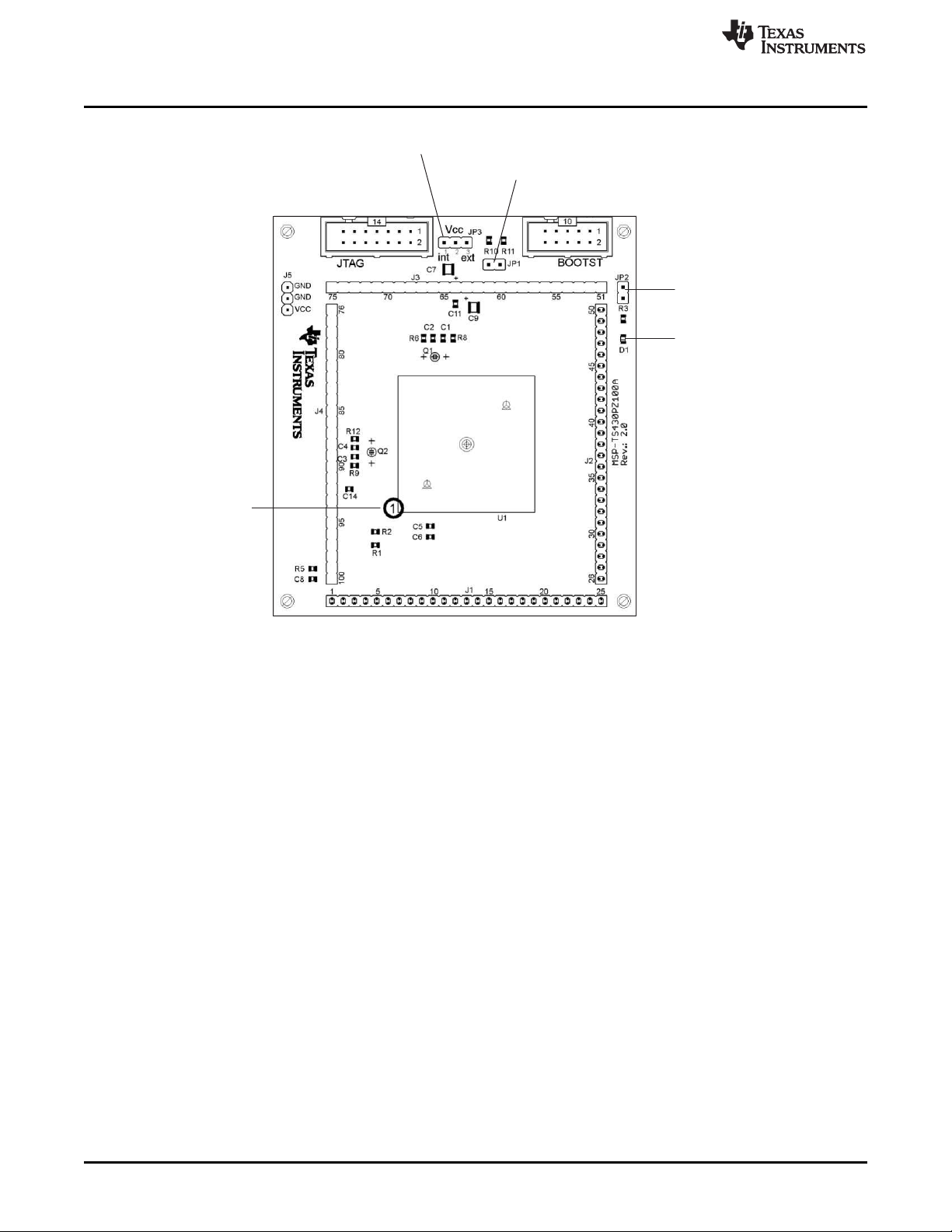
Jumper JP1
Open to measure current
Jumper JP2
Open to disconnect LED
LED D1 connected to P5.1
Jumper JP3
1-2 (int): Power supply via JTAG interface
2-3 (ext): External Power Supply
Orient Pin 1 of Device
MSP-TS430PZ100A
www.ti.com
Figure B-44. MSP-TS430PZ100A Target Socket Module, PCB
100
Hardware SLAU278F–May 2009–Revised December 2010
© 2009–2010, Texas Instruments Incorporated
Submit Documentation Feedback
 Loading...