

Page 1

User’s Guide
December 2002
SBAU077
Page 2

IMPORTANT NOTICE
Texas Instruments Incorporated and its subsidiaries (TI) reserve the right to make corrections, modifications,
enhancements, improvements, and other changes to its products and services at any time and to discontinue
any product or service without notice. Customers should obtain the latest relevant information before placing
orders and should verify that such information is current and complete. All products are sold subject to TI’s terms
and conditions of sale supplied at the time of order acknowledgment.
TI warrants performance of its hardware products to the specifications applicable at the time of sale in
accordance with TI’s standard warranty. Testing and other quality control techniques are used to the extent TI
deems necessary to support this warranty . Except where mandated by government requirements, testing of all
parameters of each product is not necessarily performed.
TI assumes no liability for applications assistance or customer product design. Customers are responsible for
their products and applications using TI components. To minimize the risks associated with customer products
and applications, customers should provide adequate design and operating safeguards.
TI does not warrant or represent that any license, either express or implied, is granted under any TI patent right,
copyright, mask work right, or other TI intellectual property right relating to any combination, machine, or process
in which TI products or services are used. Information published by TI regarding third−party products or services
does not constitute a license from TI to use such products or services or a warranty or endorsement thereof.
Use of such information may require a license from a third party under the patents or other intellectual property
of the third party, or a license from TI under the patents or other intellectual property of TI.
Reproduction of information in TI data books or data sheets is permissible only if reproduction is without
alteration and is accompanied by all associated warranties, conditions, limitations, and notices. Reproduction
of this information with alteration is an unfair and deceptive business practice. TI is not responsible or liable for
such altered documentation.
Resale of TI products or services with statements different from or beyond the parameters stated by TI for that
product or service voids all express and any implied warranties for the associated TI product or service and
is an unfair and deceptive business practice. TI is not responsible or liable for any such statements.
Mailing Address:
Texas Instruments
Post Office Box 655303
Dallas, Texas 75265
Copyright 2002, Texas Instruments Incorporated
Page 3

Contents
1 Introduction to the MSC1210 1-1. . . . . . . . . . . . . . . . . . . . . . . . . . . . . . . . . . . . . . . . . . . . . . . . . . . . .
1.1 MSC1210 Description 1-2. . . . . . . . . . . . . . . . . . . . . . . . . . . . . . . . . . . . . . . . . . . . . . . . . . . . . . .
1.2 MSC1210 Pin-Out 1-3. . . . . . . . . . . . . . . . . . . . . . . . . . . . . . . . . . . . . . . . . . . . . . . . . . . . . . . . . .
1.2.1 I/O Ports (P0, P1, P2, and P3) 1-6. . . . . . . . . . . . . . . . . . . . . . . . . . . . . . . . . . . . . . . .
1.2.2 Oscillator Inputs (XTAL1 and XTAL2) 1-9. . . . . . . . . . . . . . . . . . . . . . . . . . . . . . . . . . .
1.2.3 Reset Line (RST) 1-10. . . . . . . . . . . . . . . . . . . . . . . . . . . . . . . . . . . . . . . . . . . . . . . . . . .
1.2.4 Address Latch Enable (ALE) 1-10. . . . . . . . . . . . . . . . . . . . . . . . . . . . . . . . . . . . . . . . .
1.2.5 Program Store Enable (PSEN) 1-10. . . . . . . . . . . . . . . . . . . . . . . . . . . . . . . . . . . . . . .
1.2.6 External Access (EA) 1-11. . . . . . . . . . . . . . . . . . . . . . . . . . . . . . . . . . . . . . . . . . . . . . .
1.3 Enhanced 8051 Core 1-12. . . . . . . . . . . . . . . . . . . . . . . . . . . . . . . . . . . . . . . . . . . . . . . . . . . . . .
1.4 Family Device Compatibility 1-13. . . . . . . . . . . . . . . . . . . . . . . . . . . . . . . . . . . . . . . . . . . . . . . . .
1.5 Flash Memory 1-13. . . . . . . . . . . . . . . . . . . . . . . . . . . . . . . . . . . . . . . . . . . . . . . . . . . . . . . . . . . . .
1.6 High Performance Analog Functions 1-13. . . . . . . . . . . . . . . . . . . . . . . . . . . . . . . . . . . . . . . . .
1.7 High-Performance Peripherals 1-14. . . . . . . . . . . . . . . . . . . . . . . . . . . . . . . . . . . . . . . . . . . . . .
2 MSC1210 Memory Organization 2-1. . . . . . . . . . . . . . . . . . . . . . . . . . . . . . . . . . . . . . . . . . . . . . . . . .
2.1 Description 2-2. . . . . . . . . . . . . . . . . . . . . . . . . . . . . . . . . . . . . . . . . . . . . . . . . . . . . . . . . . . . . . . .
2.2 Program Memory 2-2. . . . . . . . . . . . . . . . . . . . . . . . . . . . . . . . . . . . . . . . . . . . . . . . . . . . . . . . . . .
2.3 Data Memory 2-4. . . . . . . . . . . . . . . . . . . . . . . . . . . . . . . . . . . . . . . . . . . . . . . . . . . . . . . . . . . . . .
2.3.1 On-Chip Extended Static RAM (SRAM) 2-4. . . . . . . . . . . . . . . . . . . . . . . . . . . . . . . . .
2.3.2 On-Chip Flash Data Memory 2-5. . . . . . . . . . . . . . . . . . . . . . . . . . . . . . . . . . . . . . . . . .
2.3.3 External Data Memory 2-5. . . . . . . . . . . . . . . . . . . . . . . . . . . . . . . . . . . . . . . . . . . . . . .
2.4 Internal RAM 2-6. . . . . . . . . . . . . . . . . . . . . . . . . . . . . . . . . . . . . . . . . . . . . . . . . . . . . . . . . . . . . . .
2.4.1 The Stack 2-7. . . . . . . . . . . . . . . . . . . . . . . . . . . . . . . . . . . . . . . . . . . . . . . . . . . . . . . . . .
2.4.2 Register Banks 2-7. . . . . . . . . . . . . . . . . . . . . . . . . . . . . . . . . . . . . . . . . . . . . . . . . . . . . .
2.4.3 Bit Memory 2-8. . . . . . . . . . . . . . . . . . . . . . . . . . . . . . . . . . . . . . . . . . . . . . . . . . . . . . . . .
2.4.4 Special Function Register (SFR) Memory 2-10. . . . . . . . . . . . . . . . . . . . . . . . . . . . . .
3 Special Function Registers (SFRs) 3-1. . . . . . . . . . . . . . . . . . . . . . . . . . . . . . . . . . . . . . . . . . . . . . . .
3.1 Description 3-2. . . . . . . . . . . . . . . . . . . . . . . . . . . . . . . . . . . . . . . . . . . . . . . . . . . . . . . . . . . . . . . .
3.2 Referencing SFRs 3-3. . . . . . . . . . . . . . . . . . . . . . . . . . . . . . . . . . . . . . . . . . . . . . . . . . . . . . . . . .
3.2.1 Referencing Bits of SFRs 3-3. . . . . . . . . . . . . . . . . . . . . . . . . . . . . . . . . . . . . . . . . . . . .
3.3 Bit−Addressable SFRs 3-4. . . . . . . . . . . . . . . . . . . . . . . . . . . . . . . . . . . . . . . . . . . . . . . . . . . . . .
3.4 SFR Types 3-4. . . . . . . . . . . . . . . . . . . . . . . . . . . . . . . . . . . . . . . . . . . . . . . . . . . . . . . . . . . . . . . . .
3.5 SFR Definitions 3-5. . . . . . . . . . . . . . . . . . . . . . . . . . . . . . . . . . . . . . . . . . . . . . . . . . . . . . . . . . . . .
4 Basic Registers 4-1. . . . . . . . . . . . . . . . . . . . . . . . . . . . . . . . . . . . . . . . . . . . . . . . . . . . . . . . . . . . . . . . .
4.1 Description 4-2. . . . . . . . . . . . . . . . . . . . . . . . . . . . . . . . . . . . . . . . . . . . . . . . . . . . . . . . . . . . . . . .
4.2 Accumulator 4-2. . . . . . . . . . . . . . . . . . . . . . . . . . . . . . . . . . . . . . . . . . . . . . . . . . . . . . . . . . . . . . .
4.3 R Registers 4-2. . . . . . . . . . . . . . . . . . . . . . . . . . . . . . . . . . . . . . . . . . . . . . . . . . . . . . . . . . . . . . . .
4.4 B Register 4-3. . . . . . . . . . . . . . . . . . . . . . . . . . . . . . . . . . . . . . . . . . . . . . . . . . . . . . . . . . . . . . . . .
4.5 Program Counter (PC) 4-3. . . . . . . . . . . . . . . . . . . . . . . . . . . . . . . . . . . . . . . . . . . . . . . . . . . . . .
4.6 Data Pointer (DPTR0/DPTR1) 4-4. . . . . . . . . . . . . . . . . . . . . . . . . . . . . . . . . . . . . . . . . . . . . . . .
4.7 Stack Pointer (SP) 4-4. . . . . . . . . . . . . . . . . . . . . . . . . . . . . . . . . . . . . . . . . . . . . . . . . . . . . . . . . .
Contents
i
Page 4

Contents
5 Addressing Modes 5-1. . . . . . . . . . . . . . . . . . . . . . . . . . . . . . . . . . . . . . . . . . . . . . . . . . . . . . . . . . . . . .
5.1 Description 5-2. . . . . . . . . . . . . . . . . . . . . . . . . . . . . . . . . . . . . . . . . . . . . . . . . . . . . . . . . . . . . . . .
5.2 Immediate Addressing 5-2. . . . . . . . . . . . . . . . . . . . . . . . . . . . . . . . . . . . . . . . . . . . . . . . . . . . . .
5.3 Direct Addressing 5-3. . . . . . . . . . . . . . . . . . . . . . . . . . . . . . . . . . . . . . . . . . . . . . . . . . . . . . . . . . .
5.4 Indirect Addressing 5-4. . . . . . . . . . . . . . . . . . . . . . . . . . . . . . . . . . . . . . . . . . . . . . . . . . . . . . . . .
5.5 External Direct Addressing 5-5. . . . . . . . . . . . . . . . . . . . . . . . . . . . . . . . . . . . . . . . . . . . . . . . . . .
5.6 External Indirect Addressing 5-6. . . . . . . . . . . . . . . . . . . . . . . . . . . . . . . . . . . . . . . . . . . . . . . . .
5.7 Code Indirect Adressing 5-6. . . . . . . . . . . . . . . . . . . . . . . . . . . . . . . . . . . . . . . . . . . . . . . . . . . . .
6 Program Flow 6-1. . . . . . . . . . . . . . . . . . . . . . . . . . . . . . . . . . . . . . . . . . . . . . . . . . . . . . . . . . . . . . . . . . .
6.1 Description 6-2. . . . . . . . . . . . . . . . . . . . . . . . . . . . . . . . . . . . . . . . . . . . . . . . . . . . . . . . . . . . . . . .
6.2 Conditional Branching 6-2. . . . . . . . . . . . . . . . . . . . . . . . . . . . . . . . . . . . . . . . . . . . . . . . . . . . . . .
6.3 Direct Jumps 6-2. . . . . . . . . . . . . . . . . . . . . . . . . . . . . . . . . . . . . . . . . . . . . . . . . . . . . . . . . . . . . . .
6.4 Direct Calls 6-4. . . . . . . . . . . . . . . . . . . . . . . . . . . . . . . . . . . . . . . . . . . . . . . . . . . . . . . . . . . . . . . .
6.5 Returns From Routines 6-4. . . . . . . . . . . . . . . . . . . . . . . . . . . . . . . . . . . . . . . . . . . . . . . . . . . . . .
6.6 Interrupts 6-4. . . . . . . . . . . . . . . . . . . . . . . . . . . . . . . . . . . . . . . . . . . . . . . . . . . . . . . . . . . . . . . . . .
7 System Timing 7-1. . . . . . . . . . . . . . . . . . . . . . . . . . . . . . . . . . . . . . . . . . . . . . . . . . . . . . . . . . . . . . . . . .
7.1 Description 7-2. . . . . . . . . . . . . . . . . . . . . . . . . . . . . . . . . . . . . . . . . . . . . . . . . . . . . . . . . . . . . . . .
7.2 System Timers 7-4. . . . . . . . . . . . . . . . . . . . . . . . . . . . . . . . . . . . . . . . . . . . . . . . . . . . . . . . . . . . .
7.2.1 Microseconds Timer 7-6. . . . . . . . . . . . . . . . . . . . . . . . . . . . . . . . . . . . . . . . . . . . . . . . .
7.2.2 Milliseconds Timer 7-6. . . . . . . . . . . . . . . . . . . . . . . . . . . . . . . . . . . . . . . . . . . . . . . . . . .
7.3 Startup Timing 7-9. . . . . . . . . . . . . . . . . . . . . . . . . . . . . . . . . . . . . . . . . . . . . . . . . . . . . . . . . . . . .
7.3.1 Normal-Mode Power-On Reset Timing 7-9. . . . . . . . . . . . . . . . . . . . . . . . . . . . . . . . .
7.3.2 Flash Programming Mode Power-On Reset Timing 7-9. . . . . . . . . . . . . . . . . . . . . .
8 Timers 8-1. . . . . . . . . . . . . . . . . . . . . . . . . . . . . . . . . . . . . . . . . . . . . . . . . . . . . . . . . . . . . . . . . . . . . . . . . .
8.1 Description 8-2. . . . . . . . . . . . . . . . . . . . . . . . . . . . . . . . . . . . . . . . . . . . . . . . . . . . . . . . . . . . . . . .
8.2 How Does a Timer Count? 8-2. . . . . . . . . . . . . . . . . . . . . . . . . . . . . . . . . . . . . . . . . . . . . . . . . . .
8.3 Using Timers to Measure Time 8-2. . . . . . . . . . . . . . . . . . . . . . . . . . . . . . . . . . . . . . . . . . . . . . .
8.3.1 How Long Does a Timer Take to Count? 8-2. . . . . . . . . . . . . . . . . . . . . . . . . . . . . . . .
8.3.2 Timer SFRs 8-4. . . . . . . . . . . . . . . . . . . . . . . . . . . . . . . . . . . . . . . . . . . . . . . . . . . . . . . . .
8.3.3 TMOD SFR 8-5. . . . . . . . . . . . . . . . . . . . . . . . . . . . . . . . . . . . . . . . . . . . . . . . . . . . . . . . .
8.3.4 TCON SFR 8-8. . . . . . . . . . . . . . . . . . . . . . . . . . . . . . . . . . . . . . . . . . . . . . . . . . . . . . . . .
8.3.5 Initializing a Timer 8-9. . . . . . . . . . . . . . . . . . . . . . . . . . . . . . . . . . . . . . . . . . . . . . . . . . .
8.3.6 Reading the Timer 8-9. . . . . . . . . . . . . . . . . . . . . . . . . . . . . . . . . . . . . . . . . . . . . . . . . . .
8.3.7 Timing the Length of Events 8-11. . . . . . . . . . . . . . . . . . . . . . . . . . . . . . . . . . . . . . . . .
8.4 Using Timers as Event Counters 8-12. . . . . . . . . . . . . . . . . . . . . . . . . . . . . . . . . . . . . . . . . . . . .
8.5 Using Timer 2 8-13. . . . . . . . . . . . . . . . . . . . . . . . . . . . . . . . . . . . . . . . . . . . . . . . . . . . . . . . . . . . .
8.5.1 T2CON SFR 8-13. . . . . . . . . . . . . . . . . . . . . . . . . . . . . . . . . . . . . . . . . . . . . . . . . . . . . . .
8.5.2 Timer 2 in Auto-Reload Mode 8-14. . . . . . . . . . . . . . . . . . . . . . . . . . . . . . . . . . . . . . . .
8.5.3 Timer 2 in Capture Mode 8-15. . . . . . . . . . . . . . . . . . . . . . . . . . . . . . . . . . . . . . . . . . . .
8.5.4 Timer 2 as a Baud Rate Generator 8-16. . . . . . . . . . . . . . . . . . . . . . . . . . . . . . . . . . . .
9 Serial Communication 9-1. . . . . . . . . . . . . . . . . . . . . . . . . . . . . . . . . . . . . . . . . . . . . . . . . . . . . . . . . . .
9.1 Description 9-2. . . . . . . . . . . . . . . . . . . . . . . . . . . . . . . . . . . . . . . . . . . . . . . . . . . . . . . . . . . . . . . .
9.2 Setting the Serial Port Mode 9-3. . . . . . . . . . . . . . . . . . . . . . . . . . . . . . . . . . . . . . . . . . . . . . . . .
9.2.1 Serial Mode 0: Synchronous Half-Duplex 9-5. . . . . . . . . . . . . . . . . . . . . . . . . . . . . . .
9.2.2 Serial Mode 1: Asynchronous Full-Duplex 9-6. . . . . . . . . . . . . . . . . . . . . . . . . . . . . .
9.2.3 Serial Mode 2: Asynchronous Full-Duplex 9-9. . . . . . . . . . . . . . . . . . . . . . . . . . . . . .
9.2.4 Serial Mode 3: Asynchronous Full-Duplex 9-11. . . . . . . . . . . . . . . . . . . . . . . . . . . . .
9.3 Setting the Serial Port Baud Rate 9-13. . . . . . . . . . . . . . . . . . . . . . . . . . . . . . . . . . . . . . . . . . . .
9.4 Writing to the Serial Port 9-15. . . . . . . . . . . . . . . . . . . . . . . . . . . . . . . . . . . . . . . . . . . . . . . . . . . .
9.5 Reading the Serial Port 9-16. . . . . . . . . . . . . . . . . . . . . . . . . . . . . . . . . . . . . . . . . . . . . . . . . . . . .
ii
Page 5

Contents
10 Interrupts 10-1. . . . . . . . . . . . . . . . . . . . . . . . . . . . . . . . . . . . . . . . . . . . . . . . . . . . . . . . . . . . . . . . . . . . . .
10.1 Description 10-2. . . . . . . . . . . . . . . . . . . . . . . . . . . . . . . . . . . . . . . . . . . . . . . . . . . . . . . . . . . . . . .
10.2 Events That Can Trigger Interrupts 10-3. . . . . . . . . . . . . . . . . . . . . . . . . . . . . . . . . . . . . . . . . . .
10.3 Enabling Interrupts 10-5. . . . . . . . . . . . . . . . . . . . . . . . . . . . . . . . . . . . . . . . . . . . . . . . . . . . . . . . .
10.4 Polling Sequence 10-6. . . . . . . . . . . . . . . . . . . . . . . . . . . . . . . . . . . . . . . . . . . . . . . . . . . . . . . . . .
10.5 Interrupt Priorities 10-7. . . . . . . . . . . . . . . . . . . . . . . . . . . . . . . . . . . . . . . . . . . . . . . . . . . . . . . . . .
10.6 Interrupt Triggering 10-8. . . . . . . . . . . . . . . . . . . . . . . . . . . . . . . . . . . . . . . . . . . . . . . . . . . . . . . .
10.7 Exiting Interrupts 10-8. . . . . . . . . . . . . . . . . . . . . . . . . . . . . . . . . . . . . . . . . . . . . . . . . . . . . . . . . .
10.8 Types of Interrupts 10-9. . . . . . . . . . . . . . . . . . . . . . . . . . . . . . . . . . . . . . . . . . . . . . . . . . . . . . . . .
10.8.1 Serial Interrupts 10-9. . . . . . . . . . . . . . . . . . . . . . . . . . . . . . . . . . . . . . . . . . . . . . . . . . . .
10.8.2 External Interrupts 10-9. . . . . . . . . . . . . . . . . . . . . . . . . . . . . . . . . . . . . . . . . . . . . . . . . .
10.8.3 Timer Interrupts 10-11. . . . . . . . . . . . . . . . . . . . . . . . . . . . . . . . . . . . . . . . . . . . . . . . . . .
10.8.4 Watchdog Interrupt 10-11. . . . . . . . . . . . . . . . . . . . . . . . . . . . . . . . . . . . . . . . . . . . . . . .
10.8.5 Auxiliary Interrupts 10-11. . . . . . . . . . . . . . . . . . . . . . . . . . . . . . . . . . . . . . . . . . . . . . . . .
10.9 Waking Up from Idle Mode 10-15. . . . . . . . . . . . . . . . . . . . . . . . . . . . . . . . . . . . . . . . . . . . . . . . .
10.10 Register Protection 10-16. . . . . . . . . . . . . . . . . . . . . . . . . . . . . . . . . . . . . . . . . . . . . . . . . . . . . . .
10.11 Common Problems with Interrupts 10-18. . . . . . . . . . . . . . . . . . . . . . . . . . . . . . . . . . . . . . . . . .
11 Pulse Width Modulator/Tone Generator 11-1. . . . . . . . . . . . . . . . . . . . . . . . . . . . . . . . . . . . . . . . . .
11.1 Description 11-2. . . . . . . . . . . . . . . . . . . . . . . . . . . . . . . . . . . . . . . . . . . . . . . . . . . . . . . . . . . . . . .
11.2 Tone Generator 11-3. . . . . . . . . . . . . . . . . . . . . . . . . . . . . . . . . . . . . . . . . . . . . . . . . . . . . . . . . . .
11.2.1 Tone Generator Waveforms 11-4. . . . . . . . . . . . . . . . . . . . . . . . . . . . . . . . . . . . . . . . . .
11.3 PWM Generator 11-5. . . . . . . . . . . . . . . . . . . . . . . . . . . . . . . . . . . . . . . . . . . . . . . . . . . . . . . . . . .
11.3.1 Example of PWM Tone Generation 11-8. . . . . . . . . . . . . . . . . . . . . . . . . . . . . . . . . . .
11.3.2 Example of PWM Tone Generation Idling 11-9. . . . . . . . . . . . . . . . . . . . . . . . . . . . . .
11.3.3 Example of Updating PWM 11-11. . . . . . . . . . . . . . . . . . . . . . . . . . . . . . . . . . . . . . . . .
12 Analog-to-Digital Converter 12-1. . . . . . . . . . . . . . . . . . . . . . . . . . . . . . . . . . . . . . . . . . . . . . . . . . . . .
12.1 Description 12-2. . . . . . . . . . . . . . . . . . . . . . . . . . . . . . . . . . . . . . . . . . . . . . . . . . . . . . . . . . . . . . .
12.2 Input Multiplexer 12-3. . . . . . . . . . . . . . . . . . . . . . . . . . . . . . . . . . . . . . . . . . . . . . . . . . . . . . . . . . .
12.3 Temperature Sensor 12-5. . . . . . . . . . . . . . . . . . . . . . . . . . . . . . . . . . . . . . . . . . . . . . . . . . . . . . .
12.4 Burnout Current Sources 12-7. . . . . . . . . . . . . . . . . . . . . . . . . . . . . . . . . . . . . . . . . . . . . . . . . . .
12.5 Input Buffer 12-8. . . . . . . . . . . . . . . . . . . . . . . . . . . . . . . . . . . . . . . . . . . . . . . . . . . . . . . . . . . . . . .
12.6 Analog Input 12-8. . . . . . . . . . . . . . . . . . . . . . . . . . . . . . . . . . . . . . . . . . . . . . . . . . . . . . . . . . . . . .
12.7 Programmable Gain Amplifier (PGA) 12-9. . . . . . . . . . . . . . . . . . . . . . . . . . . . . . . . . . . . . . . . .
12.8 Offset DAC 12-10. . . . . . . . . . . . . . . . . . . . . . . . . . . . . . . . . . . . . . . . . . . . . . . . . . . . . . . . . . . . . .
12.9 Modulator 12-10. . . . . . . . . . . . . . . . . . . . . . . . . . . . . . . . . . . . . . . . . . . . . . . . . . . . . . . . . . . . . . .
12.10 Calibration 12-11. . . . . . . . . . . . . . . . . . . . . . . . . . . . . . . . . . . . . . . . . . . . . . . . . . . . . . . . . . . . . . .
12.11 Digital Filter 12-12. . . . . . . . . . . . . . . . . . . . . . . . . . . . . . . . . . . . . . . . . . . . . . . . . . . . . . . . . . . . . .
12.11.1 Multiplexing Channels 12-14. . . . . . . . . . . . . . . . . . . . . . . . . . . . . . . . . . . . . . . . . . . . . .
12.12 Voltage Reference 12-15. . . . . . . . . . . . . . . . . . . . . . . . . . . . . . . . . . . . . . . . . . . . . . . . . . . . . . . .
12.13 Summation/Shifter Register 12-16. . . . . . . . . . . . . . . . . . . . . . . . . . . . . . . . . . . . . . . . . . . . . . . .
12.13.1 Manual Summation Mode 12-18. . . . . . . . . . . . . . . . . . . . . . . . . . . . . . . . . . . . . . . . . .
12.13.2 ADC Summation Mode 12-18. . . . . . . . . . . . . . . . . . . . . . . . . . . . . . . . . . . . . . . . . . . . .
12.13.3 Manual Shift (Divide) Mode 12-19. . . . . . . . . . . . . . . . . . . . . . . . . . . . . . . . . . . . . . . . .
12.13.4 ADC Summation with Shift (Divide) Mode 12-19. . . . . . . . . . . . . . . . . . . . . . . . . . . . .
12.14 Interrupt-Driven ADC Sampling 12-20. . . . . . . . . . . . . . . . . . . . . . . . . . . . . . . . . . . . . . . . . . . . .
12.15 Syncronizing Multiple MSC1210 Devices 12-22. . . . . . . . . . . . . . . . . . . . . . . . . . . . . . . . . . . .
12.16 Ratiometric Measurements 12-24. . . . . . . . . . . . . . . . . . . . . . . . . . . . . . . . . . . . . . . . . . . . . . . .
12.16.1 Differential Vref 12-25. . . . . . . . . . . . . . . . . . . . . . . . . . . . . . . . . . . . . . . . . . . . . . . . . . . .
Contents
iii
Page 6

Contents
13 Serial Peripheral Interface (SPI) 13-1. . . . . . . . . . . . . . . . . . . . . . . . . . . . . . . . . . . . . . . . . . . . . . . . . .
13.1 Description 13-2. . . . . . . . . . . . . . . . . . . . . . . . . . . . . . . . . . . . . . . . . . . . . . . . . . . . . . . . . . . . . . .
13.2 Functional Description 13-2. . . . . . . . . . . . . . . . . . . . . . . . . . . . . . . . . . . . . . . . . . . . . . . . . . . . . .
13.3 Clock Phase and Polarity Controls 13-4. . . . . . . . . . . . . . . . . . . . . . . . . . . . . . . . . . . . . . . . . . .
13.4 SPI Signals 13-5. . . . . . . . . . . . . . . . . . . . . . . . . . . . . . . . . . . . . . . . . . . . . . . . . . . . . . . . . . . . . . .
13.4.1 Master In Slave Out 13-5. . . . . . . . . . . . . . . . . . . . . . . . . . . . . . . . . . . . . . . . . . . . . . . . .
13.4.2 Master Out Slave In 13-5. . . . . . . . . . . . . . . . . . . . . . . . . . . . . . . . . . . . . . . . . . . . . . . . .
13.4.3 Serial Clock 13-5. . . . . . . . . . . . . . . . . . . . . . . . . . . . . . . . . . . . . . . . . . . . . . . . . . . . . . . .
13.4.4 Slave Select 13-5. . . . . . . . . . . . . . . . . . . . . . . . . . . . . . . . . . . . . . . . . . . . . . . . . . . . . . .
13.5 SPI System Errors 13-6. . . . . . . . . . . . . . . . . . . . . . . . . . . . . . . . . . . . . . . . . . . . . . . . . . . . . . . . .
13.6 Data Transfers 13-7. . . . . . . . . . . . . . . . . . . . . . . . . . . . . . . . . . . . . . . . . . . . . . . . . . . . . . . . . . . .
13.7 FIFO Operation 13-9. . . . . . . . . . . . . . . . . . . . . . . . . . . . . . . . . . . . . . . . . . . . . . . . . . . . . . . . . . .
13.8 Code Examples 13-10. . . . . . . . . . . . . . . . . . . . . . . . . . . . . . . . . . . . . . . . . . . . . . . . . . . . . . . . . .
13.8.1 SPI Master Transfer in Double-Buffer Mode using Interrupt Polling 13-10. . . . . . .
13.8.2 SPI Master Transfer in FIFO Mode using Interrupts 13-11. . . . . . . . . . . . . . . . . . . .
14 Additional MSC1210 Hardware 14-1. . . . . . . . . . . . . . . . . . . . . . . . . . . . . . . . . . . . . . . . . . . . . . . . . .
14.1 Description 14-2. . . . . . . . . . . . . . . . . . . . . . . . . . . . . . . . . . . . . . . . . . . . . . . . . . . . . . . . . . . . . . .
14.2 Low-Voltage Detect 14-2. . . . . . . . . . . . . . . . . . . . . . . . . . . . . . . . . . . . . . . . . . . . . . . . . . . . . . . .
14.2.1 Power Supply 14-3. . . . . . . . . . . . . . . . . . . . . . . . . . . . . . . . . . . . . . . . . . . . . . . . . . . . . .
14.3 Watchdog Timer 14-4. . . . . . . . . . . . . . . . . . . . . . . . . . . . . . . . . . . . . . . . . . . . . . . . . . . . . . . . . . .
14.3.1 Watchdog Timer Hardware Configuration 14-4. . . . . . . . . . . . . . . . . . . . . . . . . . . . . .
14.3.2 Enabling Watchdog Timer 14-5. . . . . . . . . . . . . . . . . . . . . . . . . . . . . . . . . . . . . . . . . . .
14.3.3 Resetting the Watchdog Timer 14-7. . . . . . . . . . . . . . . . . . . . . . . . . . . . . . . . . . . . . . .
14.3.4 Disabling Watchdog Timer 14-8. . . . . . . . . . . . . . . . . . . . . . . . . . . . . . . . . . . . . . . . . . .
14.3.5 Watchdog Timeout/Activation 14-8. . . . . . . . . . . . . . . . . . . . . . . . . . . . . . . . . . . . . . . .
15 Advanced Topics 15-1. . . . . . . . . . . . . . . . . . . . . . . . . . . . . . . . . . . . . . . . . . . . . . . . . . . . . . . . . . . . . . .
15.1 Hardware Configuration 15-2. . . . . . . . . . . . . . . . . . . . . . . . . . . . . . . . . . . . . . . . . . . . . . . . . . . .
15.1.1 Hardware Configuration Registers 15-2. . . . . . . . . . . . . . . . . . . . . . . . . . . . . . . . . . . .
15.1.2 Hardware Configuration Memory 15-5. . . . . . . . . . . . . . . . . . . . . . . . . . . . . . . . . . . . .
15.1.3 Accessing Configuration Memory in a User Program 15-5. . . . . . . . . . . . . . . . . . . .
15.2 Advanced Flash Memory 15-6. . . . . . . . . . . . . . . . . . . . . . . . . . . . . . . . . . . . . . . . . . . . . . . . . . .
15.2.1 Write Protecting Flash Program Memory 15-6. . . . . . . . . . . . . . . . . . . . . . . . . . . . . . .
15.2.2 Updating Interrupts with Reset Sector Lock 15-6. . . . . . . . . . . . . . . . . . . . . . . . . . . .
15.3 Breakpoint Generator 15-7. . . . . . . . . . . . . . . . . . . . . . . . . . . . . . . . . . . . . . . . . . . . . . . . . . . . . .
15.3.1 Configuring Breakpoints 15-7. . . . . . . . . . . . . . . . . . . . . . . . . . . . . . . . . . . . . . . . . . . . .
15.3.2 Breakpoint Auxiliary Interrupt 15-8. . . . . . . . . . . . . . . . . . . . . . . . . . . . . . . . . . . . . . . . .
15.3.3 Disabling a Breakpoint 15-8. . . . . . . . . . . . . . . . . . . . . . . . . . . . . . . . . . . . . . . . . . . . . .
15.4 Power Optimization 15-9. . . . . . . . . . . . . . . . . . . . . . . . . . . . . . . . . . . . . . . . . . . . . . . . . . . . . . . .
15.5 Flash Memory as Data Memory 15-10. . . . . . . . . . . . . . . . . . . . . . . . . . . . . . . . . . . . . . . . . . . .
15.6 Advanced Topics and Other Information 15-12. . . . . . . . . . . . . . . . . . . . . . . . . . . . . . . . . . . . .
15.6.1 Serial and Parallel Programming of the MSC1210 15-12. . . . . . . . . . . . . . . . . . . . .
15.6.2 Debugging Using the MSC1210 Boot ROM Routines 15-12. . . . . . . . . . . . . . . . . . .
15.6.3 Using MSC1210 with Raisonance Development Tools 15-12. . . . . . . . . . . . . . . . . .
15.6.4 Using the MSC1210 Evaluation Module (EVM) 15-12. . . . . . . . . . . . . . . . . . . . . . . .
iv
Page 7

Contents
16 8052 Assembly Language 16-1. . . . . . . . . . . . . . . . . . . . . . . . . . . . . . . . . . . . . . . . . . . . . . . . . . . . . . .
16.1 Description 16-2. . . . . . . . . . . . . . . . . . . . . . . . . . . . . . . . . . . . . . . . . . . . . . . . . . . . . . . . . . . . . . .
16.2 Syntax 16-2. . . . . . . . . . . . . . . . . . . . . . . . . . . . . . . . . . . . . . . . . . . . . . . . . . . . . . . . . . . . . . . . . . .
16.3 Number Bases 16-4. . . . . . . . . . . . . . . . . . . . . . . . . . . . . . . . . . . . . . . . . . . . . . . . . . . . . . . . . . . .
16.4 Expressions 16-4. . . . . . . . . . . . . . . . . . . . . . . . . . . . . . . . . . . . . . . . . . . . . . . . . . . . . . . . . . . . . . .
16.5 Operator Precedence 16-5. . . . . . . . . . . . . . . . . . . . . . . . . . . . . . . . . . . . . . . . . . . . . . . . . . . . . .
16.6 Characters and Character Strings 16-5. . . . . . . . . . . . . . . . . . . . . . . . . . . . . . . . . . . . . . . . . . . .
16.7 Changing Program Flow (LJMP, SJMP, AJMP) 16-6. . . . . . . . . . . . . . . . . . . . . . . . . . . . . . . .
16.8 Subroutines (LCALL, ACALL, RET) 16-7. . . . . . . . . . . . . . . . . . . . . . . . . . . . . . . . . . . . . . . . . .
16.9 Register Assignment (MOV) 16-8. . . . . . . . . . . . . . . . . . . . . . . . . . . . . . . . . . . . . . . . . . . . . . . .
16.10 Incrementing and Decrementing Registers (INC, DEC) 16-11. . . . . . . . . . . . . . . . . . . . . . . .
16.11 Program Loops (DJNZ) 16-12. . . . . . . . . . . . . . . . . . . . . . . . . . . . . . . . . . . . . . . . . . . . . . . . . . . .
16.12 Setting, Clearing, and Moving Bits (SETB, CLR, CPL, MOV) 16-13. . . . . . . . . . . . . . . . . . .
16.13 Bit-Based Decisions and Branching (JB, JBC, JNB, JC, JNC) 16-15. . . . . . . . . . . . . . . . . .
16.14 Value Comparison (CJNE) 16-16. . . . . . . . . . . . . . . . . . . . . . . . . . . . . . . . . . . . . . . . . . . . . . . . .
16.15 Less Than and Greater Than Comparison (CJNE) 16-17. . . . . . . . . . . . . . . . . . . . . . . . . . . .
16.16 Zero and Non-Zero Decisions (JZ/JNZ) 16-18. . . . . . . . . . . . . . . . . . . . . . . . . . . . . . . . . . . . . .
16.17 Performing Additions (ADD, ADDC) 16-18. . . . . . . . . . . . . . . . . . . . . . . . . . . . . . . . . . . . . . . . .
16.18 Performing Subtractions (SUBB) 16-20. . . . . . . . . . . . . . . . . . . . . . . . . . . . . . . . . . . . . . . . . . . .
16.19 Performing Multiplication (MUL) 16-21. . . . . . . . . . . . . . . . . . . . . . . . . . . . . . . . . . . . . . . . . . . .
16.20 Performing Division (DIV) 16-22. . . . . . . . . . . . . . . . . . . . . . . . . . . . . . . . . . . . . . . . . . . . . . . . . .
16.21 Shifting Bits (RR, RRC, RL, RLC) 16-23. . . . . . . . . . . . . . . . . . . . . . . . . . . . . . . . . . . . . . . . . . .
16.22 Bit-Wise Logical Instructions (ANL, ORL, XRL) 16-24. . . . . . . . . . . . . . . . . . . . . . . . . . . . . . .
16.23 Exchanging Register Values (XCH) 16-26. . . . . . . . . . . . . . . . . . . . . . . . . . . . . . . . . . . . . . . . .
16.24 Swapping Accumulator Nibbles (SWAP) 16-26. . . . . . . . . . . . . . . . . . . . . . . . . . . . . . . . . . . . .
16.25 Exchanging Nibbles Between Accumulator and Internal RAM (XCHD) 16-26. . . . . . . . . . .
16.26 Adjusting Accumulator for BCD Addition (DA) 16-27. . . . . . . . . . . . . . . . . . . . . . . . . . . . . . . .
16.27 Using the Stack (PUSH/POP) 16-28. . . . . . . . . . . . . . . . . . . . . . . . . . . . . . . . . . . . . . . . . . . . . .
16.28 Setting the Data Pointer DPTR (MOV DPTR) 16-30. . . . . . . . . . . . . . . . . . . . . . . . . . . . . . . . .
16.29 Reading and Writing External RAM/Data Memory (MOVX) 16-31. . . . . . . . . . . . . . . . . . . . .
16.30 Reading Code Memory/Tables (MOVC) 16-32. . . . . . . . . . . . . . . . . . . . . . . . . . . . . . . . . . . . . .
16.31 Using Jump Tables (JMP @A+DPTR) 16-34. . . . . . . . . . . . . . . . . . . . . . . . . . . . . . . . . . . . . . .
17 Keil Simulator 17-1. . . . . . . . . . . . . . . . . . . . . . . . . . . . . . . . . . . . . . . . . . . . . . . . . . . . . . . . . . . . . . . . . .
17.1 Description 17-2. . . . . . . . . . . . . . . . . . . . . . . . . . . . . . . . . . . . . . . . . . . . . . . . . . . . . . . . . . . . . . .
17.2 Timers 17-4. . . . . . . . . . . . . . . . . . . . . . . . . . . . . . . . . . . . . . . . . . . . . . . . . . . . . . . . . . . . . . . . . . .
17.2.1 Timer 0 & 1 Example 17-5. . . . . . . . . . . . . . . . . . . . . . . . . . . . . . . . . . . . . . . . . . . . . . . .
17.3 Timer 2 17-11. . . . . . . . . . . . . . . . . . . . . . . . . . . . . . . . . . . . . . . . . . . . . . . . . . . . . . . . . . . . . . . . . .
17.4 Watchdog Timer 17-12. . . . . . . . . . . . . . . . . . . . . . . . . . . . . . . . . . . . . . . . . . . . . . . . . . . . . . . . . .
17.4.1 Watchdog Reset Facility Example 17-13. . . . . . . . . . . . . . . . . . . . . . . . . . . . . . . . . . .
17.5 System Timer 17-16. . . . . . . . . . . . . . . . . . . . . . . . . . . . . . . . . . . . . . . . . . . . . . . . . . . . . . . . . . . .
17.6 Clock Control 17-16. . . . . . . . . . . . . . . . . . . . . . . . . . . . . . . . . . . . . . . . . . . . . . . . . . . . . . . . . . . .
17.7 Analog-to-Digital Converter 17-17. . . . . . . . . . . . . . . . . . . . . . . . . . . . . . . . . . . . . . . . . . . . . . . .
17.8 Summation/Shifter 17-20. . . . . . . . . . . . . . . . . . . . . . . . . . . . . . . . . . . . . . . . . . . . . . . . . . . . . . . .
17.8.1 ADC/Summation/Shifter Example 17-21. . . . . . . . . . . . . . . . . . . . . . . . . . . . . . . . . . . .
17.9 Interrupts 17-30. . . . . . . . . . . . . . . . . . . . . . . . . . . . . . . . . . . . . . . . . . . . . . . . . . . . . . . . . . . . . . . .
17.10 Ports 17-31. . . . . . . . . . . . . . . . . . . . . . . . . . . . . . . . . . . . . . . . . . . . . . . . . . . . . . . . . . . . . . . . . . . .
17.11 Serial Peripheral Interface (SPI) 17-32. . . . . . . . . . . . . . . . . . . . . . . . . . . . . . . . . . . . . . . . . . . .
17.11.1 SPI Sample Code 17-34. . . . . . . . . . . . . . . . . . . . . . . . . . . . . . . . . . . . . . . . . . . . . . . . .
17.12 mVision 2 Debug Program Example 17-38. . . . . . . . . . . . . . . . . . . . . . . . . . . . . . . . . . . . . . . . .
17.13 Serial Port I/O 17-40. . . . . . . . . . . . . . . . . . . . . . . . . . . . . . . . . . . . . . . . . . . . . . . . . . . . . . . . . . . .
17.13.1 Serial Port 0 Operation Mode 1 Example 17-42. . . . . . . . . . . . . . . . . . . . . . . . . . . . .
17.13.2 Transmit Block Baud Rate Computation 17-43. . . . . . . . . . . . . . . . . . . . . . . . . . . . . .
17.13.3 Receive Block Baud Rate Computation 17-44. . . . . . . . . . . . . . . . . . . . . . . . . . . . . . .
17.14 Additional Resource 17-46. . . . . . . . . . . . . . . . . . . . . . . . . . . . . . . . . . . . . . . . . . . . . . . . . . . . . .
Contents
v
Page 8

Contents
A Additional Features in the MSC1210 Compared to the 8052 A-1. . . . . . . . . . . . . . . . . . . . . . . . .
A.1 Additional Features in the MSC1210 Compared to 8052 A-2. . . . . . . . . . . . . . . . . . . . . . . . .
B Clock Timing Diagram B-1. . . . . . . . . . . . . . . . . . . . . . . . . . . . . . . . . . . . . . . . . . . . . . . . . . . . . . . . . . .
B.1 MSC1210 Timing Chain and Clock Control Diagram B-2. . . . . . . . . . . . . . . . . . . . . . . . . . . . .
C Boot ROM Routines C-1. . . . . . . . . . . . . . . . . . . . . . . . . . . . . . . . . . . . . . . . . . . . . . . . . . . . . . . . . . . . .
C.1 Description C-2. . . . . . . . . . . . . . . . . . . . . . . . . . . . . . . . . . . . . . . . . . . . . . . . . . . . . . . . . . . . . . . .
C.1.1 Note Regarding the put_string Function C-3. . . . . . . . . . . . . . . . . . . . . . . . . . . . . . . .
D 8052 Instruction-Set Quick-Reference Guide D-1. . . . . . . . . . . . . . . . . . . . . . . . . . . . . . . . . . . . . . .
D.1 8052 Instruction-Set Quick-Reference Guide D-2. . . . . . . . . . . . . . . . . . . . . . . . . . . . . . . . . . .
E 8052 Instruction Set E-1. . . . . . . . . . . . . . . . . . . . . . . . . . . . . . . . . . . . . . . . . . . . . . . . . . . . . . . . . . . . .
E.1 Description E-2. . . . . . . . . . . . . . . . . . . . . . . . . . . . . . . . . . . . . . . . . . . . . . . . . . . . . . . . . . . . . . . .
E.2 8052 Instruction Set E-3. . . . . . . . . . . . . . . . . . . . . . . . . . . . . . . . . . . . . . . . . . . . . . . . . . . . . . . . .
F Bit-Addressable SFRs (alphabetical) F-1. . . . . . . . . . . . . . . . . . . . . . . . . . . . . . . . . . . . . . . . . . . . . .
F.1 Bit Addressable SFRs (alphabetical) F-2. . . . . . . . . . . . . . . . . . . . . . . . . . . . . . . . . . . . . . . . . .
G SFRs/Address Cross-Reference Guide (alphabetical) G-1. . . . . . . . . . . . . . . . . . . . . . . . . . . . . .
G.1 SFR/Address Cross-Reference G-2. . . . . . . . . . . . . . . . . . . . . . . . . . . . . . . . . . . . . . . . . . . . . . .
vi
Page 9

Contents
1−1. MSC1210 Block Diagram 1-2. . . . . . . . . . . . . . . . . . . . . . . . . . . . . . . . . . . . . . . . . . . . . . . . . . . . . .
1−2. Pin Configuration of the MSC1210 1-3. . . . . . . . . . . . . . . . . . . . . . . . . . . . . . . . . . . . . . . . . . . . . .
1−3. MSC1210 Timing Compared to Standard 8051 Timing 1-12. . . . . . . . . . . . . . . . . . . . . . . . . . . .
2−1. MSC1210 Memory Map 2-2. . . . . . . . . . . . . . . . . . . . . . . . . . . . . . . . . . . . . . . . . . . . . . . . . . . . . . . .
2−2. MSC1210 Memory Map Register Bank. 2-6. . . . . . . . . . . . . . . . . . . . . . . . . . . . . . . . . . . . . . . . . .
7−1. Standard 8051 Timing. 7-2. . . . . . . . . . . . . . . . . . . . . . . . . . . . . . . . . . . . . . . . . . . . . . . . . . . . . . . . .
7−2. MSC1210 Timing Chain and Clock Control 7-5. . . . . . . . . . . . . . . . . . . . . . . . . . . . . . . . . . . . . . .
7−3. SPI/PWM/Flash Write Timing 7-5. . . . . . . . . . . . . . . . . . . . . . . . . . . . . . . . . . . . . . . . . . . . . . . . . . .
7−4. System Timing Interrupt Control 7-7. . . . . . . . . . . . . . . . . . . . . . . . . . . . . . . . . . . . . . . . . . . . . . . . .
7−5. Reset Timing 7-9. . . . . . . . . . . . . . . . . . . . . . . . . . . . . . . . . . . . . . . . . . . . . . . . . . . . . . . . . . . . . . . . .
7−6. Parallel Flash Programming Power-On Timing (EA is ignored) 7-9. . . . . . . . . . . . . . . . . . . . . .
7−7. Serial Flash Programming Power-On Timing (EA is ignored) 7-10. . . . . . . . . . . . . . . . . . . . . . .
8−1. Timer 0/1 Block Diagram for Modes 0 and 1 8-6. . . . . . . . . . . . . . . . . . . . . . . . . . . . . . . . . . . . . .
9−1. Serial Port 0 Mode 0 Transmit Timing—High Speed Operation. 9-6. . . . . . . . . . . . . . . . . . . . .
9−2. Serial Port Mode 0 Receive Timing—High Speed Operation. 9-6. . . . . . . . . . . . . . . . . . . . . . . .
9−3. Serial Port Mode 1 Transmit Timing. 9-7. . . . . . . . . . . . . . . . . . . . . . . . . . . . . . . . . . . . . . . . . . . . .
9−4. Serial Port 0 Mode 1 Receive Timing. 9-7. . . . . . . . . . . . . . . . . . . . . . . . . . . . . . . . . . . . . . . . . . . .
9−5. Serial Port 0 Mode 2 Transmit Timing. 9-9. . . . . . . . . . . . . . . . . . . . . . . . . . . . . . . . . . . . . . . . . . .
9−6. Serial Port 0 Mode 2 Receive Timing. 9-10. . . . . . . . . . . . . . . . . . . . . . . . . . . . . . . . . . . . . . . . . . .
9−7. Serial Port 0 Mode 3 Transmit Timing. 9-11. . . . . . . . . . . . . . . . . . . . . . . . . . . . . . . . . . . . . . . . . .
9−8. Serial Port 0 Mode 3 Receive Timing. 9-11. . . . . . . . . . . . . . . . . . . . . . . . . . . . . . . . . . . . . . . . . . .
11−1. Block Diagram 11-2. . . . . . . . . . . . . . . . . . . . . . . . . . . . . . . . . . . . . . . . . . . . . . . . . . . . . . . . . . . . . . .
11−2. Tone Generator Circuit 11-3. . . . . . . . . . . . . . . . . . . . . . . . . . . . . . . . . . . . . . . . . . . . . . . . . . . . . . . .
11−3. Timing Diagram of Tone Generator in Staircase Mode 11-4. . . . . . . . . . . . . . . . . . . . . . . . . . . .
11−4. Timing Diagram of Tone Generator in Square Wave Mode 11-4. . . . . . . . . . . . . . . . . . . . . . . . .
11−5. Timing Diagram of a PWM Waveform 11-6. . . . . . . . . . . . . . . . . . . . . . . . . . . . . . . . . . . . . . . . . . .
11−6. PWM Timing 11-11. . . . . . . . . . . . . . . . . . . . . . . . . . . . . . . . . . . . . . . . . . . . . . . . . . . . . . . . . . . . . . .
12−1. MSC1210 Architecture 12-2. . . . . . . . . . . . . . . . . . . . . . . . . . . . . . . . . . . . . . . . . . . . . . . . . . . . . . . .
12−2. Input Multiplexer Configuration 12-3. . . . . . . . . . . . . . . . . . . . . . . . . . . . . . . . . . . . . . . . . . . . . . . . .
12−3. Basic Input Structure of the MSC1210 12-8. . . . . . . . . . . . . . . . . . . . . . . . . . . . . . . . . . . . . . . . . .
12−4. Filter Step Responses 12-12. . . . . . . . . . . . . . . . . . . . . . . . . . . . . . . . . . . . . . . . . . . . . . . . . . . . . . .
12−5. Filter Frequency Responses 12-13. . . . . . . . . . . . . . . . . . . . . . . . . . . . . . . . . . . . . . . . . . . . . . . . . .
12−6. Circuit Drawing 12-24. . . . . . . . . . . . . . . . . . . . . . . . . . . . . . . . . . . . . . . . . . . . . . . . . . . . . . . . . . . . .
13−1. SPI block diagram 13-2. . . . . . . . . . . . . . . . . . . . . . . . . . . . . . . . . . . . . . . . . . . . . . . . . . . . . . . . . . . .
13−2. SPI Clock/Data Timing 13-3. . . . . . . . . . . . . . . . . . . . . . . . . . . . . . . . . . . . . . . . . . . . . . . . . . . . . . . .
13−3. SPI Reset State 13-7. . . . . . . . . . . . . . . . . . . . . . . . . . . . . . . . . . . . . . . . . . . . . . . . . . . . . . . . . . . . . .
13−4. SPI FIFO Operation 13-9. . . . . . . . . . . . . . . . . . . . . . . . . . . . . . . . . . . . . . . . . . . . . . . . . . . . . . . . . .
14−1. Brownout Reset and Low-Voltage Detection 14-2. . . . . . . . . . . . . . . . . . . . . . . . . . . . . . . . . . . . .
14−2. System Timing Interrupt Control 14-4. . . . . . . . . . . . . . . . . . . . . . . . . . . . . . . . . . . . . . . . . . . . . . . .
Contents
vii
Page 10

Contents
16−1. Rotate Operations 16-23. . . . . . . . . . . . . . . . . . . . . . . . . . . . . . . . . . . . . . . . . . . . . . . . . . . . . . . . . . .
17−1. Timer/Counter 0 − Mode 2 17-4. . . . . . . . . . . . . . . . . . . . . . . . . . . . . . . . . . . . . . . . . . . . . . . . . . . .
17−2. Timer/Counter 0 17-5. . . . . . . . . . . . . . . . . . . . . . . . . . . . . . . . . . . . . . . . . . . . . . . . . . . . . . . . . . . . .
17−3. Parallel Port 3 Peripheral 17-5. . . . . . . . . . . . . . . . . . . . . . . . . . . . . . . . . . . . . . . . . . . . . . . . . . . . . .
17−4. Timer/Counter 1 Mode 1 17-6. . . . . . . . . . . . . . . . . . . . . . . . . . . . . . . . . . . . . . . . . . . . . . . . . . . . . .
17−5. Interrupt System 17-6. . . . . . . . . . . . . . . . . . . . . . . . . . . . . . . . . . . . . . . . . . . . . . . . . . . . . . . . . . . . .
17−6. Timer/Counter 2 17-11. . . . . . . . . . . . . . . . . . . . . . . . . . . . . . . . . . . . . . . . . . . . . . . . . . . . . . . . . . . .
17−7. Status of Watchdog Peripheral 17-12. . . . . . . . . . . . . . . . . . . . . . . . . . . . . . . . . . . . . . . . . . . . . . . .
17−8. Analog−to−Digital Converter Peripheral 17-18. . . . . . . . . . . . . . . . . . . . . . . . . . . . . . . . . . . . . . . .
17−9. Error Message 17-19. . . . . . . . . . . . . . . . . . . . . . . . . . . . . . . . . . . . . . . . . . . . . . . . . . . . . . . . . . . . . .
17−10. Accumulator/Shifter Peripheral 17-20. . . . . . . . . . . . . . . . . . . . . . . . . . . . . . . . . . . . . . . . . . . . . . . .
17−11. summation/Shifter Peripheral 17-28. . . . . . . . . . . . . . . . . . . . . . . . . . . . . . . . . . . . . . . . . . . . . . . . .
17−12. The ADC Peripheral Mid-Stride a Typical 8-Sample Averaging Block 17-28. . . . . . . . . . . . . .
17−13. List Box for the Interrupt Peripheral 17-30. . . . . . . . . . . . . . . . . . . . . . . . . . . . . . . . . . . . . . . . . . . .
17−14. Parallel Port 0 Contents Display Window 17-31. . . . . . . . . . . . . . . . . . . . . . . . . . . . . . . . . . . . . . .
17−15. Error Message 17-31. . . . . . . . . . . . . . . . . . . . . . . . . . . . . . . . . . . . . . . . . . . . . . . . . . . . . . . . . . . . . .
17−16. SPI Peripheral Window 17-32. . . . . . . . . . . . . . . . . . . . . . . . . . . . . . . . . . . . . . . . . . . . . . . . . . . . . .
17−17. Keil Debugger 17-39. . . . . . . . . . . . . . . . . . . . . . . . . . . . . . . . . . . . . . . . . . . . . . . . . . . . . . . . . . . . . .
17−18. Serial Channel 0 Communication Peripheral 17-41. . . . . . . . . . . . . . . . . . . . . . . . . . . . . . . . . . . .
17−19. Clock Control Peripheral 17-45. . . . . . . . . . . . . . . . . . . . . . . . . . . . . . . . . . . . . . . . . . . . . . . . . . . . .
17−20. USART0 Preipheral 17-45. . . . . . . . . . . . . . . . . . . . . . . . . . . . . . . . . . . . . . . . . . . . . . . . . . . . . . . . .
B−1. MSC1210 Timing Chain and Clock Control B-2. . . . . . . . . . . . . . . . . . . . . . . . . . . . . . . . . . . . . . .
viii
Page 11

Contents
1−1. Pin Descriptions of the MSC1210 1-4. . . . . . . . . . . . . . . . . . . . . . . . . . . . . . . . . . . . . . . . . . . . . . .
2−1. Program and Data Memory Size. 2-3. . . . . . . . . . . . . . . . . . . . . . . . . . . . . . . . . . . . . . . . . . . . . . . .
2−2. Program and Data Memory Addresses. 2-4. . . . . . . . . . . . . . . . . . . . . . . . . . . . . . . . . . . . . . . . . .
3−1. SFR Names and Addresses. 3-2. . . . . . . . . . . . . . . . . . . . . . . . . . . . . . . . . . . . . . . . . . . . . . . . . . .
5−1. MSC1210 Addressing Modes. 5-2. . . . . . . . . . . . . . . . . . . . . . . . . . . . . . . . . . . . . . . . . . . . . . . . . .
7−1. Signal Definitions for Reset Timing Diagrams 7-10. . . . . . . . . . . . . . . . . . . . . . . . . . . . . . . . . . . .
8−1. Timer Conrol SFRs. 8-4. . . . . . . . . . . . . . . . . . . . . . . . . . . . . . . . . . . . . . . . . . . . . . . . . . . . . . . . . . .
8−2. Timer Modes and Usage 8-6. . . . . . . . . . . . . . . . . . . . . . . . . . . . . . . . . . . . . . . . . . . . . . . . . . . . . . .
8−3. Example of 8-Bit Auto-Reload 8-7. . . . . . . . . . . . . . . . . . . . . . . . . . . . . . . . . . . . . . . . . . . . . . . . . .
8−4. TCON (88h) SFR 8-8. . . . . . . . . . . . . . . . . . . . . . . . . . . . . . . . . . . . . . . . . . . . . . . . . . . . . . . . . . . . .
9−1. SM0 and SM1 Function Definitions. 9-4. . . . . . . . . . . . . . . . . . . . . . . . . . . . . . . . . . . . . . . . . . . . .
9−2. Common Baud Rates Using Timer 1 9-8. . . . . . . . . . . . . . . . . . . . . . . . . . . . . . . . . . . . . . . . . . . . .
9−3. Common Baud Rates Using Timer 2 9-9. . . . . . . . . . . . . . . . . . . . . . . . . . . . . . . . . . . . . . . . . . . . .
9−4. Mode 0 Commonly Used Baud Rates. 9-13. . . . . . . . . . . . . . . . . . . . . . . . . . . . . . . . . . . . . . . . . .
9−5. Baud Rate Settings for Timer 1. 9-14. . . . . . . . . . . . . . . . . . . . . . . . . . . . . . . . . . . . . . . . . . . . . . . .
9−6. Baud Rate Settings for Timer 2. 9-15. . . . . . . . . . . . . . . . . . . . . . . . . . . . . . . . . . . . . . . . . . . . . . . .
10−1. Interrupt Sources 10-3. . . . . . . . . . . . . . . . . . . . . . . . . . . . . . . . . . . . . . . . . . . . . . . . . . . . . . . . . . . .
10−2. IE (A8h) SFR 10-5. . . . . . . . . . . . . . . . . . . . . . . . . . . . . . . . . . . . . . . . . . . . . . . . . . . . . . . . . . . . . . . .
10−3. EICON (D8h) SFR 10-5. . . . . . . . . . . . . . . . . . . . . . . . . . . . . . . . . . . . . . . . . . . . . . . . . . . . . . . . . . .
10−4. EIE (E8h) SFR 10-5. . . . . . . . . . . . . . . . . . . . . . . . . . . . . . . . . . . . . . . . . . . . . . . . . . . . . . . . . . . . . . .
10−5. IP (B8h) SFR 10-7. . . . . . . . . . . . . . . . . . . . . . . . . . . . . . . . . . . . . . . . . . . . . . . . . . . . . . . . . . . . . . . .
10−6. EIP (F8h) SFR 10-7. . . . . . . . . . . . . . . . . . . . . . . . . . . . . . . . . . . . . . . . . . . . . . . . . . . . . . . . . . . . . . .
10−7. EXIF (91h) SFR 10-10. . . . . . . . . . . . . . . . . . . . . . . . . . . . . . . . . . . . . . . . . . . . . . . . . . . . . . . . . . . . .
10−8. Clearing Auxiliary Interrupts 10-12. . . . . . . . . . . . . . . . . . . . . . . . . . . . . . . . . . . . . . . . . . . . . . . . . .
10−9. AIE (A6h) SFR 10-12. . . . . . . . . . . . . . . . . . . . . . . . . . . . . . . . . . . . . . . . . . . . . . . . . . . . . . . . . . . . . .
10−10. AISTAT (A7h) SFR 10-13. . . . . . . . . . . . . . . . . . . . . . . . . . . . . . . . . . . . . . . . . . . . . . . . . . . . . . . . . .
10−11. PAI (A5h) SFR 10-13. . . . . . . . . . . . . . . . . . . . . . . . . . . . . . . . . . . . . . . . . . . . . . . . . . . . . . . . . . . . . .
10−12. PPI Bits of PAI SFR 10-14. . . . . . . . . . . . . . . . . . . . . . . . . . . . . . . . . . . . . . . . . . . . . . . . . . . . . . . . .
10−13. EWU (C6h) SFR 10-15. . . . . . . . . . . . . . . . . . . . . . . . . . . . . . . . . . . . . . . . . . . . . . . . . . . . . . . . . . . .
11−1. PWM Polarity Conditions 11-5. . . . . . . . . . . . . . . . . . . . . . . . . . . . . . . . . . . . . . . . . . . . . . . . . . . . . .
11−2. Configuring the PWM for Tone Generation 11-8. . . . . . . . . . . . . . . . . . . . . . . . . . . . . . . . . . . . . . .
11−3. Statement Explanations 11-8. . . . . . . . . . . . . . . . . . . . . . . . . . . . . . . . . . . . . . . . . . . . . . . . . . . . . . .
11−4. Configuring the PWM for Tone Generation with PWM Idling 11-10. . . . . . . . . . . . . . . . . . . . . . .
11−5. Statement Explanations 11-10. . . . . . . . . . . . . . . . . . . . . . . . . . . . . . . . . . . . . . . . . . . . . . . . . . . . . .
12−1. PGA Settings 12-9. . . . . . . . . . . . . . . . . . . . . . . . . . . . . . . . . . . . . . . . . . . . . . . . . . . . . . . . . . . . . . . .
12−2. Calibration Mode Control Bits 12-11. . . . . . . . . . . . . . . . . . . . . . . . . . . . . . . . . . . . . . . . . . . . . . . . .
12−3. Filter Settling 12-14. . . . . . . . . . . . . . . . . . . . . . . . . . . . . . . . . . . . . . . . . . . . . . . . . . . . . . . . . . . . . . .
12−4. Output Data Rate and Channel Rate 12-14. . . . . . . . . . . . . . . . . . . . . . . . . . . . . . . . . . . . . . . . . . .
12−5. Output Data Rate and Channel Rate (10x faster) 12-15. . . . . . . . . . . . . . . . . . . . . . . . . . . . . . . .
Contents
ix
Page 12

Contents
14−1. Typical Sub-Circuit Current Consumption 14-3. . . . . . . . . . . . . . . . . . . . . . . . . . . . . . . . . . . . . . . .
14−2. Comparator Specification 14-3. . . . . . . . . . . . . . . . . . . . . . . . . . . . . . . . . . . . . . . . . . . . . . . . . . . . .
14−3. Band Gap Parameters 14-3. . . . . . . . . . . . . . . . . . . . . . . . . . . . . . . . . . . . . . . . . . . . . . . . . . . . . . . .
16−1. Order of Precedence for Mathematical Operators 16-5. . . . . . . . . . . . . . . . . . . . . . . . . . . . . . . .
16−2. Results of ANL 16-24. . . . . . . . . . . . . . . . . . . . . . . . . . . . . . . . . . . . . . . . . . . . . . . . . . . . . . . . . . . . .
16−3. Results of ORL 16-24. . . . . . . . . . . . . . . . . . . . . . . . . . . . . . . . . . . . . . . . . . . . . . . . . . . . . . . . . . . . .
16−4. Results of XRL 16-24. . . . . . . . . . . . . . . . . . . . . . . . . . . . . . . . . . . . . . . . . . . . . . . . . . . . . . . . . . . . .
17−1. Timer/Counter 2 Control Bits 17-11. . . . . . . . . . . . . . . . . . . . . . . . . . . . . . . . . . . . . . . . . . . . . . . . . .
C−1. Boot ROM Routines C-2. . . . . . . . . . . . . . . . . . . . . . . . . . . . . . . . . . . . . . . . . . . . . . . . . . . . . . . . . . .
x
Page 13

Chapter 1
This chapter describes the basic function of the MSC1210 analog-to-digital
converter (ADC).
Topic Page
1.1 MSC1210 Description 1-2. . . . . . . . . . . . . . . . . . . . . . . . . . . . . . . . . . . . . . . . .
1.2 MSC1210 Pin-Out 1-3. . . . . . . . . . . . . . . . . . . . . . . . . . . . . . . . . . . . . . . . . . . . .
1.3 Enhanced 8051 Core 1-12. . . . . . . . . . . . . . . . . . . . . . . . . . . . . . . . . . . . . . . . .
1.4 Family Device Compatibility 1-13. . . . . . . . . . . . . . . . . . . . . . . . . . . . . . . . . .
1.5 Flash Memory 1-13. . . . . . . . . . . . . . . . . . . . . . . . . . . . . . . . . . . . . . . . . . . . . . .
1.6 High-Performance Analog 1-13. . . . . . . . . . . . . . . . . . . . . . . . . . . . . . . . . . . .
1.7 High-Performance Peripherals 1-14. . . . . . . . . . . . . . . . . . . . . . . . . . . . . . . .
Introduction to the MSC1210
1-1
Page 14

MSC1210 Description
1.1 MSC1210 Description
The MicroSystem family of devices is designed for high-resolution measurement applications in smart transmitters, industrial process control, weigh
scales, chromatography, and portable instrumentation. They provide highperformance mixed signal solutions. The MicroSystem family not only includes high-end analog features and digital processing capability, but also integrates high-performance peripherals to offer a unique system solution.
The main components of a MicroSystem product include:
- Enhanced 8051 microcontroller core
- FLASH memory
- High-performance analog functions
- High-performance peripherals
The enhanced 8052 microcontroller core includes dual data pointers and executes instructions three times faster than the standard 8052 core. This MIPS
capability allows you to optimize speed, power, and noise tradeoffs based on
specific requirements.
A block diagram of the MSC1210 ADC is shown in Figure 1−1.
Figure 1−1.MSC1210 Block Diagram
1-2
Page 15
The on-chip FLASH memory is programmable in a variety of modes over a
wide temperature and operating voltage range. This greatly simplifies programming at both the manufacturing level and in the field.
The on-chip high-performance analog features are state-of-the-art. The perfor mance and f eatures o f t he a nalog f unctions r ival t he b est o f t he i ndustry. The l ownoise ADC and the precision voltage reference a long w ith t he integration o f o ther
analog features greatly simplify achieving high-end analog performance.
The on-chip high-performance peripherals not only reduce the cost, design
time, and board space required for external circuitry, but also blend analog and
digital functions that simplify the system design. The high-performance peripherals are designed from a system perspective, thereby decreasing the processing requirements on the CPU and providing greater system throughput.
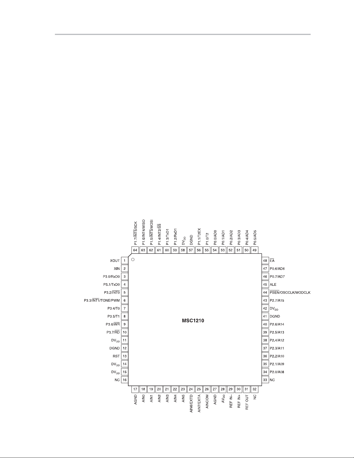
1.2 MSC1210 Pin-Out
The names and functions of these pins are similar to those found on a
traditional 8052 core, but the MSC1210 includes additional pin assignments
to support the additional functions specific to the part.
MSC1210 Pin-Out
Figure 1−2.Pin Configuration of the MSC1210
Introduction to the MSC1210
1-3
Page 16

MSC1210 Pin-Out
Table 1−1.Pin Descriptions of the MSC1210
Pin # Name Description
1 XOUT The crystal oscillator pin XOUT supports parallel resonant AT cut crys-
tals and ceramic resonators. XOUT serves as the output of the crystal
amplifier.
2 XIN The crystal oscillator pin XIN supports parallel resonant AT cut crystals
and ceramic resonators. XIN can also be an input if there is an external
clock source instead of a crystal.
3-10 P3.0-P3.7 Port 3 is a bidirectional I/O port. The alternate functions for Port3 are
listed below.
Port 3—Alternate Functions:
PORT ALTERNATE MODE
P3.0 RxD0 Serial Port 0 Input
P3.1 TxD0 Serial Port 0 Output
P3.2 INT0 External Interrupt 0
P3.3 INT1/TONE/
PWM
P3.4 T0 Timer 0 External Input
P3.5 T1 Timer 1 External Input
P3.6 WR External Data Memory Write Strobe
P3.7 RD External Data Memory Read Strobe
External Interrupt 1/TONE/PWM Output
11, 14, 15,
DV
DD
Digital Power Supply
42, 58
12, 41, 57 DGND Digital Ground
13 RST A HIGH on the reset input for two instruction clock cycles will reset the
device.
16, 32, 33 NC No Connection
17, 27 AGND Analog Ground
28 AV
DD
Analog Power Supply
18 AIN0 Analog Input Channel 0
19 AIN1 Analog Input Channel 1
20 AIN2 Analog Input Channel 2
21 AIN3 Analog Input Channel 3
22 AIN4 Analog Input Channel 4
23 AIN5 Analog Input Channel 5
24 AIN6, EXTD Analog Input Channel 6, Digital Low Voltage Detect Input
25 AIN7, EXTA Analog Input Channel 7, Analog Low Voltage Detect Input
26 AINCOM Analog Common for Single−Ended Inputs
29 REF IN– Voltage Reference Negative Input
30 REF IN+ Voltage Reference Positive Input
31 REF OUT Voltage Reference Output
1-4
Page 17
MSC1210 Pin-Out
Table 1−1 Pin Descriptions of the MSC1210 (Continued)
Pin # Name Description
34-40, 43 P2.0-P2.7 Port 2 is a bidirectional I/O port. The alternate functions for Port 2 are
listed below.
Port 2—Alternate Functions:
34-40, 43 P2.0-P2.7 PORT ALTERNATE MODE
P2.0 A8 Address Bit 8
P2.1 A9 Address Bit 9
P2.2 A10 Address Bit 10
P2.3 A11 Address Bit 11
P2.4 A12 Address Bit 12
P2.5 A13 Address Bit 13
P2.6 A14 Address Bit 14
P2.7 A15 Address Bit 15
44 PSEN, OSCCLK,
MODCLK
45 ALE Address Latch Enable: Used for latching the low byte of the address
48 EA External Access Enable: EA must be externally held LOW to enable
46, 47,
P0.0−P0.7 Port 0 is a bidirectional I/O port. The alternate functions for Port 0 are
49-54
Program Store Enable: Connected to optional external memory as a
chip enable. PSEN
mode, PSEN
allel programming mode. PSEN
will provide an active low pulse. In programming
is used as an input along with ALE to define serial or par-
is held HIGH for parallel programming
and tied LOW for serial programming. This pin can also be selected
(when not using external program memory) to output the Oscillator
clock, Modulator clock, HIGH, or LOW.
ALE PSEN Program Mode Selection
NC NC Normal Operation
0 1 Parallel Programming
1 0 Serial Programming
0 0 Reserved
during an access to external memory. ALE is emitted at a constant rate
of 1/2 the oscillator frequency, and can be used for external timing or
clocking. One ALE pulse is skipped during each access to external
data memory. In programming mode, ALE is used as an input along
with PSEN
to define serial or parallel programming mode. ALE is held
HIGH for serial programming and tied LOW for parallel programming.
the device to fetch code from external program memory locations starting with 0000
.
H
listed below.
Port 0—Alternate Functions:
PORT ALTERNATE MODE
P0.0 AD0 Address/Data Bit 0
P0.1 AD1 Address/Data Bit 1
P0.2 AD2 Address/Data Bit 2
P0.3 AD3 Address/Data Bit 3
P0.4 AD4 Address/Data Bit 4
Introduction to the MSC1210
1-5
Page 18

MSC1210 Pin-Out
Table 1−1 Pin Descriptions of the MSC1210 (Continued)
Pin # Name Description
46, 47,
49-54
55, 56,
59−64
P0.0−P0.7 P0.5 AD5 Address/Data Bit 5
P0.6 AD6 Address/Data Bit 6
P0.7 AD7 Address/Data Bit 7
P1.0−P1.7 Port 1 is a bidirectional I/O port. The alternate functions for Port 1 are
listed below.
Port 1—Alternate Functions:
PORT ALTERNATE MODE
P1.0 T2 T2 Input
P1.1 T2EX T2 External Input
P1.2 RxD1 Serial Port Input
P1.3 TxD1 Serial Port Output
P1.4 INT2/SS External Interrupt/Slave Select
P1.5 INT3/MOSI External Interrupt/Master Out−Slave In
P1.6 INT4/MISO External Interrupt/Master In−Slave Out
P1.7 INT5/SCK External Interrupt/Serial Clock
1.2.1 I/O Ports (P0, P1, P2, and P3)
Of the 64 pins on the MSC1210, 32 of them are dedicated to I/O lines that have
a one-to-one relation with SFRs P0, P1, P2, and P3. The developer may raise
and lower these lines by writing 1s or 0s to the corresponding bits in the SFRs.
Likewise, the current state of these lines may be found by reading the corresponding bits of the SFRs.
All of the ports have optional pull-up resistors that are enabled when the port
is in 8051 mode, as configured by the PxDDRL/H SFRs. The pull-up resistors
are disabled when the port is configured in any other mode, or when accessing
external memory.
1.2.1.1 Port 0
Port 0 is dual-function: in some designs port 0 I/O lines are available to the developer to access external devices, while in other designs it is used to access
external memory. If the circuit requires external RAM, the microcontroller will
use port 0 to latch in/out the 8-bit data word, as well as the low eight bits of the
address in response to a MOVX instruction, as long as the hardware configuration registers are set up correctly . Port 0 I/O lines may be used for other functions as long as external data memory is not being accessed at the same time
and the hardware configuration registers are set up correctly. If the circuit requires external code memory, the microcontroller will use port 0 I/O lines to access each instruction to be executed. In this case, port 0 cannot be used for
other purposes, because the state of the I/O lines are constantly being modified to access external code memory.
1-6
Page 19

1.2.1.2 Port 1
MSC1210 Pin-Out
Port 1 consists of eight I/O lines that may be used to interface to external parts.
Port 1 is commonly used to interface to external hardware such as LCDs, keypads, and other devices. As opposed to a standard 8052 core, all I/O lines of
the MSC1210 serve optional alternate functions, as described below. These
lines can still be used for the developing purposes, if the functions described
below are not needed.
P1.0 (T2): If T2CON.1 is set (C/T
2), then timer 2 is incremented whenever
there is a 1-0 transition on this line. With C/T2 set, P1.0 is the clock source for
timer 2.
P1.1 (T2EX): If timer 2 is in auto-reload mode and T2CON.3 (EXEN2) is set,
a 1-0 transition on this line causes timer 2 to be reloaded with the auto-reload
value. This also causes the T2CON.6 (EXF2) external flag to be set, which
may cause an interrupt, if so enabled.
P1.2 (RxD1): If the secondary USART is b eing used, P 1.2 (RxD1) i s the p in that
receives serial data. Data received via this pin is read using the SBUF1 SFR.
P1.3 (TxD1): If the secondary USART is being used, P1.3 (TxD1) is the pin that
transmits serial data. Data written to the SBUF1 SFR is sent via this pin.
P1.4 (INT2/SS
): This pin has two dual functions. It may be used to trigger an
external 2 interrupt when a 0-1 transition is detected on this line. It is also used
as slave select in SPI applications.
P1.5 (INT3
/MOSI): This pin may be used to trigger an external 3 interrupt when
a 1-0 transition is detected. It is also used as Master Out/Slave In in SPI applications.
P1.6 (INT4/MISO): This pin may be used to trigger an external 4 interrupt when
a 0-1 transition is detected. It is also used as Master In/Slave Out in SPI applications.
P1.7 (INT5/SCK): This pin may be used to trigger an external 5 interrupt when
a 1-0 transition is detected. It is also used as serial clock in SPI applications.
Introduction to the MSC1210
1-7
Page 20

MSC1210 Pin-Out
1.2.1.3 Port 2
Like port 0, port 2 is dual-function. I n some c ircuit designs, it i s available f or accessing external devices, while in others it is used to address external RAM or external
code memory . W hen m ore t han 256 b ytes o f e xternal RA M are u sed, p ort 2 i s used
to output the high byte of the address that is to be accessed in a MOVX operation.
Whether port 2 is used to address external memory or as general I/O lines is defined by the EGP23 bit in hardware configuration Register 1.
Note:
When the EGP23 bit of hardware configuration Register 1 is set, Port 2 assumes the value of the high byte of DPTR when using the MOVX @DPTR
instruction. When using the MOVX @Rx instructions, port 2 assumes the value of the MPAGE SFR.
If the circuit requires external code memory, the microcontroller automatically uses
port 2 I/O lines to access each instruction to be executed, but only if bit EGP23
of HCR1 equals one. In this case, port 2 cannot be used for other purposes because the state of the I/O lines are constantly being modified to access external
code memory.
1.2.1.4 Port 3
Port 3 consists entirely of dual-function I/O lines. While you can access all
these lines from the software by reading/writing to the P3 SFR, each pin has
a predefined function that the microcontroller handles automatically when configured to do so and/or when necessary.
P3.0 (RxD0): The primary USART/serial port uses P3.0 as the receive line. For
in-circuit designs that are using the microcontroller internal serial port, this is
the line into which the serial data is clocked.
Note:
When interfacing an 8052 to an RS-232 port, you cannot connect this line
directly to the RS-232 pin; you must pass it through a part such as the
MAX233 to obtain the correct voltage levels.
You can assign any function to this pin as long as the circuit has no need to
receive data via the integrated serial port.
P3.1 (TxD0): The primary USART/serial port uses P3.1 as the transmit line. For
in-circuit designs t hat i s u sing t he m icrocontroller i nternal s erial p ort, t his i s t he l ine
used by the microcontroller to clock out all data written to the SBUF SFR.
Note:
1-8
When interfacing an 8052 to an RS-232 port, you cannot connect this line
directly to the RS-232 pin; you must pass it through a part such as the
MAX233 to obtain the correct voltage levels.
You can assign any function to this pin as long as the circuit has no need to
transmit data via the integrated serial port.
Page 21

MSC1210 Pin-Out
P3.2 (INT0): When so configured, this line is used to trigger an external 0 Interrupt. This may either be low-level triggered or may be triggered on a 1-0 transition (see Chapter 10, Interrupts, for details). You can assign any function to this
pin as long as the circuit has no need to trigger an external 0 interrupt.
P3.3 (INT1
/TONE/PWM): When so configured, this line is used to trigger an
external 1 Interrupt. This may either be low-level triggered or may be triggered
on a 1-0 transition (see Chapter 10, Interrupts, for details). This pin is also used
for outputting PWM, if so configured.
P3.4 (T0): When so configured, this line is used as the clock source for timer 0.
Timer 0 is incremented either e very i nstruction cycle t hat T 0 i s h igh, o r e very t ime
there is a 1 -0 t ransition o n t his l ine, d epending o n h ow t he t imer i s c onfigured ( see
Chapter 8, Timers, for details). You c an a ssign a ny function to this pin a s l ong a s
the circuit has no need to control timer 0 externally.
P3.5 (T1): When so configured, this line is used as the clock source for timer 1.
Timer 1 is incremented either e very i nstruction cycle t hat T 1 i s h igh, o r e very t ime
there is a 1 -0 t ransition o n t his l ine, d epending o n h ow t he t imer i s c onfigured ( see
Chapter 8, Timers, for details). You can assign a ny f unction t o t h is p in a s l ong a s
the circuit has no need to control timer 1 externally.
P3.6 (WR
): This is the external memory write strobe line when bit EGP23 is
set in hardware configuration Register 1. This line is asserted low by the microcontroller whenever a MOVX instruction writes to external RAM. This line
should be connected to the RAM write (W
) line. You can assign any function
to this pin as long as the circuit does not write to external RAM using MOVX.
P3.7 (RD
): This is the external memory read strobe line when bit EGP23 is set
in hardware configuration Register 1. This line is asserted low by the microcontroller whenever a MOVX instruction is read from external RAM. This line must
be connected to the RAM read (R
) line. You can assign any function to this pin
as long as the circuit does not read from external RAM using MOVX.
1.2.2 Oscillator Inputs (XTAL1 and XTAL2)
The MSC1210 is typically driven by a crystal connected to pins 1 (XOUT) and
2 (XIN). Common crystal frequencies are 11.0592MHz as well as 12MHz, although the MSC1210 is capable of accepting frequencies as high as 33MHz.
While a crystal is the normal clock source, this is not always the case. A digital
clock source may also be attached to XIN and XOUT to provide the clock for
the microcontroller.
Introduction to the MSC1210
1-9
Page 22

MSC1210 Pin-Out
1.2.3 Reset Line (RST)
Pin 13 is the master reset line for the microcontroller. When this pin is brought
high for two instruction cycles, the microcontroller is effectively reset. SFRs,
including the I/O ports, are restored to their default conditions and the program
counter is reset to 0000
a reset. The microcontroller begins executing code at 0000
turns to a low state.
The reset line is often connected to a reset button/switch that you can press
to reset the circuit. It is also common to connect the reset line to a watchdog
IC or a supervisor IC (such as MAX707). Traditional resistor-capacitor networks attached to the reset line also work well because the RST input is a
Schmitt trigger input.
1.2.4 Address Latch Enable (ALE)
The ALE at pin 45 is an output-only pin that is controlled entirely by the microcontroller and allows the microcontroller to multiplex the low-byte of a memory
address and the 8-bit data itself on port 0. This is because, while the high byte
of the memory address is sent on port 2, port 0 is used both to send the low
byte of the memory address and the data itself. This is accomplished by placing the low byte of the address on port 0, exerting an ALE high-to-low transition
to latch the low byte of the address into a latch IC (such as the 74HC573), and
then placing the 8 data bits on port 0. In this way, the MSC1210 is able to output
a 16-bit address and an 8-bit data word with 16 I/O lines instead of 24.
. Keep in mind that Internal RAM is not affected by
H
when pin 13 re-
H
The ALE line is used in this fashion both to access external RAM with MOVX
@DPTR, as well as t o a ccessi instructions i n e xternal c ode memory. When t he p rogram is executed from external code memory, ALE pulses at a rate that is ¼ that
of the oscillator frequency. Thus, if the oscillator operates at 11.0592MHz, ALE
pulses at a rate of 2 764 800 t imes per s econd. When t he MOVX i nstruction is e xecuted, one PSEN
pulse is missed in lieu of a pulse on WR or RD.
This pin is also used when programming the part, along with PSEN
during reset to indicate whether programming will occur in serial or parallel
mode. If this line is held high when in programming mode, programming will
occur in serial mode.
1.2.5 Program Store Enable (PSEN)
The program store enable (PSEN) line at pin 44 is exerted low automatically
by the microcontroller whenever it accesses external code memory. This line
should be attached to the output enable (OE
your code memory. The PSEN signal is applied for both internal and external
memory access.
This pin is also used when p rogramming the p art, along w ith A LE, as a n i nput to
indicate whether programming will occur in serial or parallel mode. If this line is
held high when in programming mode, programming will occur in parallel mode.
, as an input
) pin of the device that contains
1-10
Page 23

1.2.6 External Access (EA)
The external access (EA) line at pin 48 is used to determine whether the
MSC1210 will execute your program from external code memory or from internal code memory. I f E A
will execute the program it finds in internal/on-chip code memory. If EA
low (to ground), it will attempt to execute the program that it finds in the attached external program memory. Of course, the external program memory
must be properly connected for the microcontroller to be able to access the
program in external program memory.
MSC1210 Pin-Out
is tied high (connected to supply), the microcontroller
is tied
The EA
pin is ignored during serial or parallel flash programming modes.
Note:
Even when EA
is tied high (indicating that the microcontroller should execute
from internal code memory), the microcontroller will attempt to execute from
external code memory if the program counter references an address not
available for the chip you are using, or if you are accessing program memory
in excess of the amount of flash memory that you have partitioned for program memory. For example, if you have partitioned 4k of flash memory to be
program memory and you tie EA
high, the derivative starts executing the program it finds on-chip. However, if your on-chip program attempts to execute
code above 0FFF
(that is, exceeding 4k), then the MSC1210 will attempt
H
to execute that code at that address from external code memory. Thus, it is
possible to have a split design, in which some of the code is found on-chip
and the rest is found off-chip.
Introduction to the MSC1210
1-11
Page 24
Enhanced 8051 Core
1.3 Enhanced 8051 Core
The MSC1210 is an 8052-based family of high-performance, mixed-signal
controllers. All instructions in the MSC1210 family perform exactly the same
function as they would in a standard 8052 core. Although the effect on bits,
flags, and registers is the same, the timing is different.
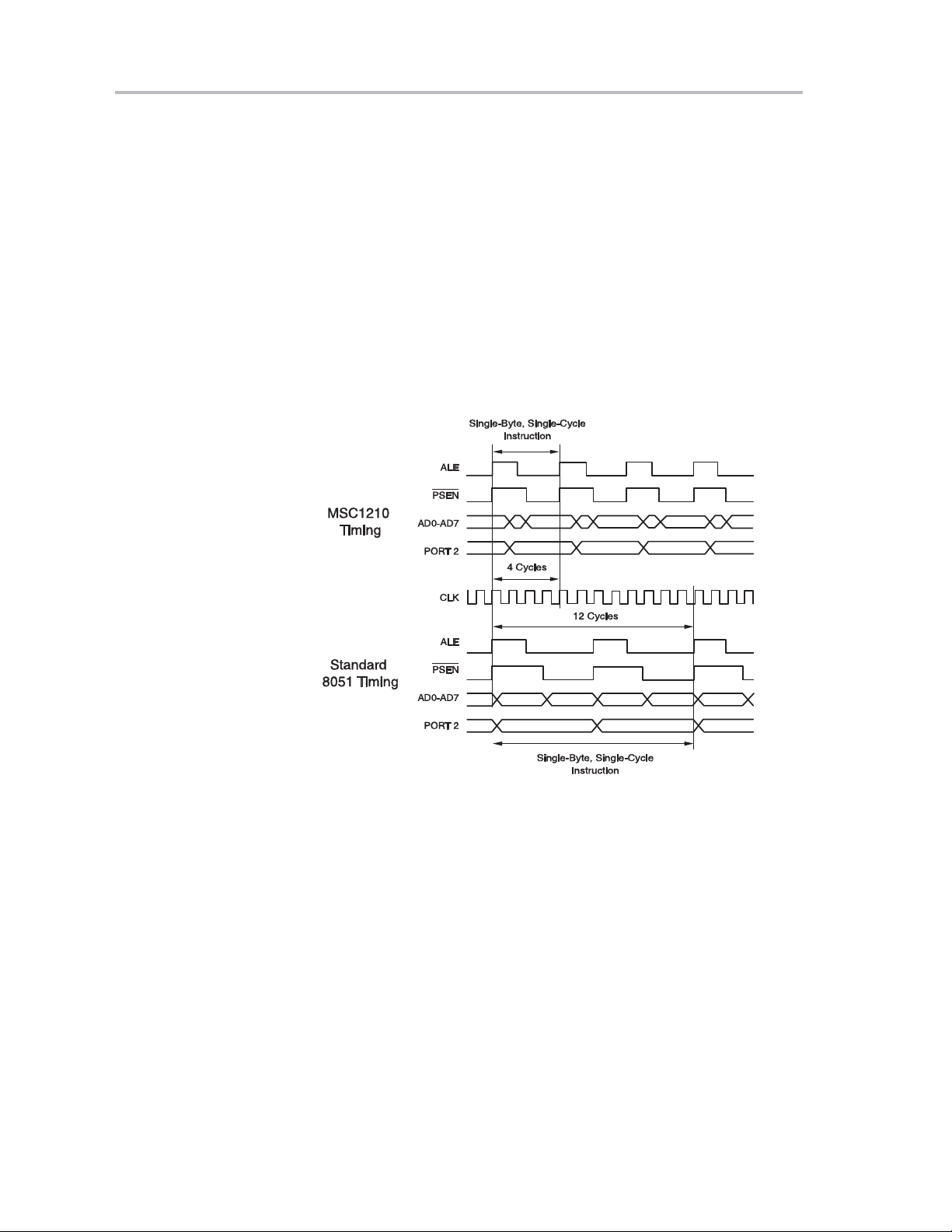
The MSC1210 family uses an efficient 8052 core that results in an improved
instruction execution speed of three times faster than the original core for the
same external clock speed (4 clock cycles per instruction versus 12 clock
cycles per instruction, as shown in Figure 1−3). This allows you to run the device at slower external clock speeds, which reduces system noise and power
consumption, but provides greater throughput.
Figure 1−3.MSC1210 Timing Compared to Standard 8051 Timing
1-12
The timing of software loops is faster with the MSC1210 than with the standard
8052. However , t he t imer/counter o peration o f t he M SC1210 m ay b e m aintained
at 12 clocks per increment or optionally run at 4 clocks per increment.
You can develop software for the MSC1210 with the existing 8052 development tools because the MSC1210 is fully compatible with the standard 8052
instruction set. Additionally, a complete integrated development environment
is provided with each demonstration board.
Page 25

1.4 Family Device Compatibility
The hardware functionality and pin outs across the MSC1210 family are fully
compatible. The only difference between family members is the memory configuration and this enables simple migration between family members. Code
written for the 4K bytes program memory version of the MSC1210 can be executed directly on the 8K, 16K, or 32K versions. This allows you to add or delete
software functions and to freely migrate between family members.
The MSC1210 can become a standard device used across several application
platforms.
1.5 Flash Memory
The MSC1210 features flexible flash memory that allows you to uniquely configure the program and non-volatile data memory maps to meet the needs of
the application. The flash memory is programmable over the entire operating
voltage range and temperature range using both serial and parallel programming methods.
Family Device Compatibility
1.6 High Performance Analog Functions
The analog functionality is state-of-the-art. The ADC is extremely low noise,
which enables you to meet even the most stringent analog requirements. The
integrated programmable gain amplifier (PGA) further improves the performance of the ADC. This effectively provides for resolution into the nanovolt
range.
The on-chip voltage reference provides for low drift and high accuracy, thus
eliminating the need for an external voltage reference.
These features are integrated with other analog functions, such as a programmable filter, multiplexer, temperature sensor , burnout current sources, analog
input buffer, and an offset correction digital-to-analog converter (DAC).
Introduction to the MSC1210
1-13
Page 26

High-Performance Peripherals
1.7 High-Performance Peripherals
High-performance peripherals are included on-chip, which offload CPU processing and control functions from the core to further improve the overall device
efficiency and throughput. On-chip peripherals include additional SRAM, a
32-bit accumulator, an SPI-compatible serial port with a FIFO buffer, dual
USARTs, on-chip power-on reset, brownout reset, low-voltage detect, multiple
digital ports with configurable I/O, a 16-bit pulse width modulator (PWM), a
watchdog timer, and three timer/counters.
For instance, the SPI interface uses a FIFO buffer, which allows for the serial
transmission and reception of data with virtually no CPU overhead. The FIFO
buffer function allows for the transfer of large amounts of data at faster transfer
rates than more conventional methods.
Additionally, the 32-bit accumulator significantly reduces the processing overhead for the multiple byte data from the ADC or other sources. This allows for
24-bit addition, subtraction, and shifting to be accomplished without using
CPU resources. This can reduce both the code size and code execution time.
1-14
Page 27

Chapter 2
This chapter defines the Memory Organization of MSC1210 ADC.
Topic Page
2.1 Description 2-2. . . . . . . . . . . . . . . . . . . . . . . . . . . . . . . . . . . . . . . . . . . . . . . . . . .
2.2 Program Memory 2-2. . . . . . . . . . . . . . . . . . . . . . . . . . . . . . . . . . . . . . . . . . . . .
2.3 Data Memory 2-4. . . . . . . . . . . . . . . . . . . . . . . . . . . . . . . . . . . . . . . . . . . . . . . . .
2.4 Internal RAM 2-6. . . . . . . . . . . . . . . . . . . . . . . . . . . . . . . . . . . . . . . . . . . . . . . . .
MSC1210 Memory Organization
2-1
Page 28
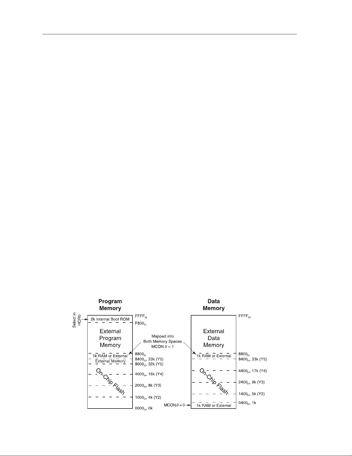
Description
2.1 Description
The MCS1210 has three very general types of memory. To program the
MCS1210 effectively, it is necessary to have a basic understanding of these
memory types:
- Special Function Registers refer to 128 bytes that control the operation
of the MSC1210.
- Program Memory is used to store the actual program that may reside on-
chip, off-chip, or both.
- Data Memory is static random access memory (SRAM) that can reside
on-chip, off-chip, or both. The MSC1210 has four types of data memory:
J On-chip extended SRAM
J Off-chip external SRAM
J On-chip Flash Data memory
J Internal RAM
2.2 Program Memory
Program memory holds the actual program that is to be run. This memory includes the on-chip flash memory designated as program memory and/or external memory.
The MSC1210 family offers a maximum of 32k of on-chip flash program
memory. The exact amount of on-chip program memory depends on the specific MSC1210 version selected and how the flash memory of that chip has
been partitioned between program and data memory. Figure 2−1 illustrates
how the flash memory may be distributed between these two types of memory.
Figure 2−1.MSC1210 Memory Map
2-2
Page 29

For example, in the Y5 model there is 32k flash memory available. This 32k
may be configured as either program memory, data memory, or both. This configuration is set at the moment the firmware is loaded onto the MSC1210 by
setting hardware configuration register HCR0 as per Table 2−1. This table indicates the total amount of program and data memory available for each part
revision given a specific HCR0 setting.
Table 2−1.Program and Data Memory Size.
HCR0 MSC1210Y2 MSC1210Y3 MSC1210Y4 MSC1210Y5
DFSEL PM DM PM DM PM DM PM DM
000 0kB 4kB 0kB 8kB 0kB 16kB 0kB 32kB
001 0kB 4kB 0kB 8kB 0kB 16kB 0kB 32kB
010 0kB 4kB 0kB 8kB 0kB 16kB 16kB 16kB
011 0kB 4kB 0kB 8kB 8kB 8kB 24kB 8kB
100 0kB 4kB 4kB 4kB 12kB 4kB 28kB 4kB
101 2kB 2kB 6kB 2kB 14kB 2kB 30kB 2kB
110 3kB 1kB 7kB 1kB 15kB 1kB 31kB 1kB
111 (default) 4kB 0kB 8kB 0kB 16kB 0kB 32kB 0kB
Program Memory
Note: When a 0kB program memory configuration is selected, program execution is external
For example, setting the DFSEL bits to 1 10 with a MSC1210Y5 would cause
31kb of on-chip flash memory to be partitioned as program memory and 1kb
of flash memory to be partitioned as data memory.
Table 2−2 indicates where the assigned memory will be located in address
space. This table provides essentially the same information as Table 2−1, but
also indicates where the memory will be located. For example, the DFSEL =
110 example in the previous paragraph (31kb of on-chip flash program
memory , 1k of on-chip flash data memory) appears in Table 2−2 as flash program mem o r y f r o m 0 0 0 0
to 07FFH (which is 1k).
0400
H
Note that the Data memory address starts at 0400
to 7BFFH (which is 31k) and flash data memory from
H
because the first 1k
H
(0000H-03FFH) is, by default, used to address the on-chip extended SRAM.
The location of on-chip extended SRAM may be changed by using the Memory
Control (MCON) SFR. By setting bit 0 of MCON, the on-chip extended SRAM
may be moved from 0000
tended flash data memory always begins at 0400
-03FFH to 8400H-87FFH. However, on-chip ex-
H
regardless of whether or
H
not SRAM is located at 0000H or 8400H.
MSC1210 Memory Organization
2-3
Page 30

Data Memory
Table 2−2.Program and Data Memory Addresses.
HCR0 MSC1210Y2 MSC1210Y3 MSC1210Y4 MSC1210Y5
DFSEL PM DM PM DM PM DM PM DM
000 (reserved) — — — — — — — —
001 — — — — — — 0000 0400-83FF
010 — — — — 0000 0400-43FF 0000-3FFF 0400-43FF
011 — — 0000 0400-23FF 0000-1FFF 0400-23FF 0000-5FFF 0400-23FF
100 0000 0400-13FF 0000-0FFF 0400-13FF 0000-2FFF 0400-13FF 0000-6FFF 0400-13FF
101 0000-07FF 0400-00BF 0000-17FF 0400-0BFF 0000-37FF 0400-0BFF 0000-77FF 0400-0BFF
110 0000-00BF 0400-07FF 0000-1BFF 0400-07FF 0000-3BFF 0400-07FF 0000-7BFF 0400-07FF
111 (default) 0000-0FFF 0000 0000-1FFF 0000 0000-3FFF 0000 0000-7FFF 0000
Note: Program accesses above the highest listed address will access external Program memory.
Program memory addressing beyond the on-chip address range is accessed
externally via ports 0 and 2. The total amount of code memory, on-chip and off,
is limited to 64k due to limitations of the 8052 architecture.
Note:
2.3 Data Memory
MSC1210 programs are limited to 64k because code memory is restricted to
64k. Some c ompilers o ffer w ays t o g et around this limit w hen u sed w ith s pecially
wired hardware. However, without such special compilers and hardware, programs are limited to 64k.
The MSC1210 includes 2k of boot ROM code that controls operation during
serial or parallel programming. In program mode, the boot ROM is located in
the first 2kB of program memory.
The boot ROM is available to your program as long as EBR (hardware configuration register 0, bit 4) is set, which is the default. When enabled, the boot ROM
routines will be located at program memory addresses F800
-FFFFH. The
H
boot ROM includes a number of functions such as flash memory access, and
serial routines including data transmission, reception, and auto-baud.
Data memory is divided into four types of memory, depending on its location
and volatility: internal RAM, on-chip extended SRAM, off-chip external SRAM,
and on-chip flash data memory. However, data memory (regardless of its location or volatility) is accessed using the MOVX instruction, except for internal
RAM, which is accessed using the MOV instruction.
2.3.1 On-Chip Extended Static RAM (SRAM)
The MSC1210 includes 1024 bytes of on-chip extended static RAM (SRAM).
Even though t his m emory r esides o n-chip, i t i s a ccessed u sing t he M OVX i nstruction as if it were external data memory. Whenever a program accesses data
memory addresses 0000
2-4
through 03FFH, the on-chip external SRAM is used.
H
Page 31

On-chip extended static RAM provides 1k of data memory that requires no external circuitry and is available regardless of how the MSC1210’s flash
memory is designated. This makes it a convenient memory area for purposes
such as temporary buffers, calculation scratchpads, or any other purpose that
requires 1k o r less of memory, but does not require it to survive a power failure.
2.3.2 On-Chip Flash Data Memory
In addition to the on-chip extended SRAM described in the previous section,
the MSC1210 also has the capability of offering on-chip flash data memory.
Flash memory is slower than SRAM, but has the advantage of being nonvolatile: its contents will not be lost when the power source is removed.
All of the parts in the MSC1210 family come with some amount of on-chip flash
memory, ranging from 4k for the MSC1210Y2 all the way up to 32k for the
MSC1210Y5. This flash memory may be configured such that it can be used
as either program memory, data memory, or both.
When configured as data memory, on-chip flash data memory is accessed
starting at address 0400
For example, if the MSC1210Y5 is configured to use 2k as on-chip flash data
memory , addresses 0000
while addresses 0400H through 0BFFH will access on-chip flash data memory.
Any attempts to read data memory with addresses 0C00
in the part attempting to fetch that data off-chip from external data memory (see
the next section), e xcept w hen the i nternal 1 kB S RAM i s c onfigured a s Von Neumann type, which occupies from 8400
Data Memory
—immediately after on-chip SRAM.
H
through 03FFH will access on-chip extended SRAM
H
and higher will result
H
∼87FFH.
H
2.3.3 External Data Memory
The MSC1210 is capable of addressing up to 64k of data memory, however,
a maximum of 33k of that may be on-chip: 1k of SRAM and up to 32k of flash
data memory. If additional data memory is necessary, it must be added to the
circuit as external data memory.
External data memory is any off-chip data memory that is connected to the
MSC1210 via ports 0 and 2 and uses control pins ALE, RD
two ports combined with these three control lines allow the MSC1210 to address external RAM.
External data memory can also be used to access “memory mapped devices,”
which are devices that appear to the MSC1210 to be external data memory
but in reality are external components such as LCDs, buttons, keypads, etc.
Note:
The MSC1210 must only address 64kB of RAM. To expand RAM beyond this
limit requires programming and hardware tricks. It may be necessary to do this
“by hand” because many compilers and assemblers, while providing support for
programmers in excess of 64kB, do not support more than 6 4kB of R AM. If more
than 64kB of RAM is necessary, the compiler must be checked to verify that the
excess RAM is supported. If not, it will be necessary to do it “by hand.”
, and WR. These
MSC1210 Memory Organization
2-5
Page 32

Internal RAM
Figure 2−2.MSC1210 Memory Map Register Bank.
2.4 Internal RAM
As shown in Figure 2−2, the MSC1210 has a bank of 256 bytes of internal
RAM. This internal RAM is found on-chip within the IC, so it is the fastest RAM
available and is also the most flexible in terms of reading, writing, and modifying its contents. internal RAM is volatile, so when the MSC1210 is powered up,
the contents of this memory bank is random.
The 256 bytes of internal RAM are subdivided as shown in the memory map
of Figure 2−2. The first eight bytes (00
) are register bank 0. By manipu-
H−07H
lating certain SFRs, a program may choose to use register banks 0, 1, 2, or
3. These alternative register banks are located in internal RAM at addresses
through 1FH. Register banks are described in greater detail in chapters
08
H
3 and 4. For now it is sufficient to know that they reside in and are part of internal RAM.
Bit memory also resides in and is part of internal RAM. Bit memory will be described more in section 2.4.3, but for now just keep in mind that bit memory
actually resides in internal RAM at addresses 20
The 208 bytes remaining of internal RAM, from addresses 30
through 2FH.
H
through FFH,
H
may be used by user variables that need to be accessed frequently or at
high-speed. This area is also used by the microcontroller as a storage area for
the operating stack. This fact limits the MSC1210 stack because, as illustrated
in the memory map of Figure 2−2, the area reserved for the stack is only 208
bytes—and usually it is less because these 208 bytes have to be shared
between the stack and user variables.
Note:
Internal RAM addresses 00
addressing or indirect addressing, whereas internal RAM addresses 80
through 7FH may be accessed either via direct
H
H
through FFH may only be accessed via indirect addressing. This will be discussed completely in Chapter 5, Addressing Modes.
2-6
Page 33

2.4.1 The Stack
Internal RAM
The stack is a “last in, first out” (LIFO) storage area that exists in internal RAM.
It is used by the MSC1210 to store values that the user program manually
pushes onto the stack, as well as to store the return addresses for CALLs and
interrupt service routines (ISRs)—more on these topics later.
The stack is defined and controlled by an SFR called SP. As a standard 8−bit
SFR, SP holds a value between 0 and 255 that represents the internal RAM
address of the end of the current stack. If a value is removed from the stack,
it is taken from the internal RAM address pointed to by SP, and SP will subsequently be decremented by 1. If a value is pushed onto the stack, SP is first
incremented and then the value is inserted in internal RAM at the address now
pointed to by SP.
SP is initialized to 07
first value to be pushed onto the stack is placed at internal RAM address 08
(07H + 1), the second is placed at 09H, etc.
2.4.2 Register Banks
The MSC1210 uses eight R r egisters, w hich a re u sed i n m any o f i ts i nstructions.
These R registers are numbered from 0 through 7 (R0, R1, R2, R3, R 4, R5, R 6,
and R7) and a re g enerally u sed t o a ssist i n m anipulating v alues a nd m oving d ata
from one memory l ocation t o a nother. For example, t o a dd t he v alue o f R 4 t o t he
accumulator, the following assembly language instruction would be executed:
when the MSC1210 is first powered up. This means the
H
Note:
By default, the MSC1210 initializes the stack pointer (SP) to 07
when the
H
microcontroller is reset. This means that the stack will start at address 08
and expand upwards. If using the alternate register banks (banks 1, 2, or 3)
the stack pointer must be initialized to an address above the highest register
bank being used. Otherwise, the stack will overwrite the alternate register
banks. Similarly , i f using bit variables, it is usually a good idea to initialize the
stack pointer to some value greater than 2F
to ensure that the bit variables
H
are protected from the stack. Following is more information about the register
banks and bit memory.
H
H
ADD A,R4
Thus, if the accumulator (A) contains the value 6, and R4 contains the value 3,
the accumulator will contain the value 9 after this instruction is executed.
However, as the m emory m ap o f F igure 2−2 illustrates, R Register R4 is really
part of internal RAM. Specifically, R4 is address 04
of internal RAM. This can
H
be seen in the bright green s ection o f t he m emory map. T he a bove i nstruction,
therefore, accomplishes the same thing as the following operation:
ADD A,04h
This instruction adds the value f ound i n i nternal R AM a ddress 0 4H to the value
of the accumulator, leaving the r esult i n t he a ccumulator. The above instruction
effectively accomplishes the same thing as the previous ADD instruction because R4 is really internal RAM address 04
MSC1210 Memory Organization
.
H
2-7
Page 34

Internal RAM
But watch o ut! A s t he m emory m ap s hows, t he M SC1210 h as f our d istinct r egister
banks. When the M SC1210 i s f irst r eset, register b ank 0 ( addresses 0 0H through
) is used by default. However, the MSC1210 may be instructed to use one
07
H
of the alternate register b anks ( i.e., r egister b anks 1 , 2 , o r 3 ). I n t his c ase, R 4 will
no longer b e t he s ame a s i nternal R AM a ddress 0 4
. For e xample, i f t he p rogram
H
instructs the 8052 to use register bank 1, register R4 is now synonymous with
internal RAM address 0C
, and if register bank 3 is selected, it is synonymous with address 1CH.
14
H
. If register bank 2 i s s elected, R 4 i s s ynonymous w ith
H
The concept of register banks adds a great level of flexibility to the 8052, especially when dealing with interrupts (see chapter 10, Interrupts, for details).
However, always remember that the register banks really reside in the first 32
bytes of internal RAM.
Note:
2.4.3 Bit Memory
If only the first register bank (i.e. bank 0) is used, internal RAM locations 08
H
through 1FH can be used by the program for its own use. If register banks
1, 2, or 3 are to be used, be very careful about using addresses below 20H
to avoid overwriting the value of “R” registers from other register banks.
The MSC1210, being a communications and control-oriented microcontroller
that often has to deal with on and off situations, gives you the ability to access
a number of bit variables directly with simple instructions to set, clear, and
compare these bits. These variables may be either 1 or 0.
There are 128 bit variables available to the user , numbered 00
through 7FH.
H
The user may make use of these variables with commands such as SETB and
CLR. For example, to set bit number 24
(hex) to 1, the user would execute
H
the instruction:
SETB 24h
It is important to note that Bit memory, like the register banks in section 2.4.2,
is really a part of internal RAM. In fact, the 128-bit variables occupy the 16 bytes of internal RAM from 20
through 2FH. Thus, if the value FFH is written to
H
internal RAM address 20H, bits 00H through 07H have been effectively set.
That is to say that the instruction:
2-8
MOV 20h,#0FFh
is equivalent to the instructions:
SETB 00h
SETB 01h
SETB 02h
SETB 03h
SETB 04h
SETB 05h
SETB 06h
SETB 07h
Page 35

Internal RAM
As shown, bit memory is not really a new type of memory, it is just a subset of
internal RAM. However, because the MSC1210 provides special instructions
to access these 16 bytes of memory on a bit-by-bit basis, it is useful to think
of it as a separate type of memory. Always keep in mind that it is just a subset
of internal RAM, and that operations performed on internal RAM can change
the values of the bit variables.
Note:
If your program does not use bit variables, you may use internal RAM locations
through 2FH for your own use. When using bit variables, be very careful
20
H
about using addresses from 20
through 2FH, as you may end up overwriting
H
the value of your bits.
Note:
By default, the MSC1210 initializes SP to 07
booted. This means that the stack will start at address 08
when the microcontroller is
H
and expand up -
H
wards. If using t he a lternate r egister b anks ( banks 1, 2 o r 3 ), S P m ust b e i nitialized to an address above the highest register bank being used. Otherwise the
stack will overwrite the alternate register banks. Similarly, if using bit variables,
it is u sually a g ood i dea t o i nitialize S P t o s ome v alue g reater t han 2 F
to ensure
H
that the bit variables are protected from the stack.
Bit memory 00H through 7FH is for user-defined functions in their programs.
Bit memory 80
and above are used to access certain SFRs (see section
H
2.4.4) on a bit-by-bit basis. For example, if output lines P0.0 through P0.7 are
all clear (0), to turn on the P0.0 output line, either execute:
MOV P0,#01h
or execute:
SETB 80h
Both these instructions accomplish the same thing. However, using the SETB
command will turn on the P0.0 line without affecting the status of any of the
other P0 output lines. The MOV command effectively turns off all the other output lines that, in some cases, may not be acceptable.
When dealing with bit addresses of 80
and above, remember that the bits re -
H
fer to the bits of corresponding SFRs that are divisible by eight. This is a complicated way of saying that bits 80
, bits 88H through 8FH refer to bits 0 through 7 of SFR 88H, bits 90H through
80
H
refer to bits 0 through 7 of 90H, etc.
97
H
through 87H refer to bits 0 through 7 of SFR
H
MSC1210 Memory Organization
2-9
Page 36

Internal RAM
2.4.4 Special Function Register (SFR) Memory
SFRs are areas of memory that control specific functionality of the MSC1210.
For example, four SFRs permit access to the 32 input/output lines (eight lines
per SFR) of the MSC1210. Another SFR allows a program to read or write to
the MSC1210 serial port. Other SFRs allow the user to set the serial baud rate,
control and access timers, and configure the MSC1210 interrupt system.
When programming, SFRs have the illusion of being internal memory . For example, if writing the value 1 to internal RAM location 50
tion:
MOV 50h,#01h
Similarly, if writing the value 1 to the MSC1210 serial port, write this value to
the SBUF SFR, which has an SFR address of 99
to the serial port, execute the instruction:
MOV 99h,#01h
As shown, it appears as if the SFR is part of internal memory. This is not the
case. When using this method of memory access (it is called direct address-
ing—more on that soon), any instruction that has an address of 00
refers to an internal RAM memory address; any instruction with an ad-
7F
H
dress of 80H through FFH refers to an SFR control register.
, execute the instruc-
H
. Thus, to write the value 1
H
through
H
Note:
SFRs are used to control the way the MSC1210 functions. Each SFR has a
specific purpose and format that will be discussed later. Not all addresses
above 80H are assigned to SFRs. However, this area may not be used as
additional RAM memory, even if a given address has not been assigned to
an SFR.
Note:
Direct access addressing cannot be used to access internal RAM addresses
through FFH because direct access to addresses 80H through FFH re-
80
H
fers to SFRs. The upper 128 bytes of internal RAM must be accessed using
indirect addressing, which is explained in Chapter 5, Addressing Modes.
2-10
Page 37

Chapter 3
!
Chapter 3 defines the MSC1210 SFRs.
Topic Page
3.1 Description 3-2. . . . . . . . . . . . . . . . . . . . . . . . . . . . . . . . . . . . . . . . . . . . . . . . . . .
3.2 Referencing SFRs 3-3. . . . . . . . . . . . . . . . . . . . . . . . . . . . . . . . . . . . . . . . . . . . .
3.3 Bit-Addressable SFRs 3-4. . . . . . . . . . . . . . . . . . . . . . . . . . . . . . . . . . . . . . . . .
3.4 SFR Types 3-4. . . . . . . . . . . . . . . . . . . . . . . . . . . . . . . . . . . . . . . . . . . . . . . . . . . .
3.5 SFR Definitions 3-5. . . . . . . . . . . . . . . . . . . . . . . . . . . . . . . . . . . . . . . . . . . . . . .
Special Function Registers (SFRs)
3-1
Page 38

Description
3.1 Description
The MSC1210 is a flexible microcontroller with a relatively large number of
modes of operation. Your program may inspect and/or change the operating
mode of the MSC1210 by manipulating the values of its SFRs.
SFRs are accessed as if they were normal internal RAM. The only difference
is that internal RAM is addressed in direct mode with addresses 00
, whereas SFR registers are accessed in the range of 80H through FFH.
7F
H
through
H
Each SFR has an address (80
−FFH) and a name. Table 3−1 provides a
H
graphical presentation of the 8052’s SFRs, their names, and their address.
Although the address range of 80
through FFH offers 128 possible address-
H
es, there are 24 addresses that are not assigned to an SFR, as shown in
Table 3−1.
Note:
Reading an unassigned SFR will get 00
, and writing to an unassigned SFR
H
is ignored.
Table 3−1.SFR Names and Addresses.
80 P0 SP DPL0 DPH0 DPL1 DPH1 DPS PCON 87
88 TCON TMOD TL0 TL1 TH0 TH1 CKCON MWS 8F
90 P1 EXIF MPAGE CADDR CDATA MCON 97
98 SCON0 SBUF0 SPICON SPIDATA SPIRCON SPITCON SPISTART SPIEND 9F
A0 P2 PWMCON PWMLOW PWMHI PAI AIE AISTAT A7
A8 IE BPCON BPL BPH P0DDRL P0DDRH P1DDRL P1DDRH AF
B0 P3 P2DDRL P2DDRH P3DDRL P3DDRH B7
B8 IP BF
C0 SCON1 SBUF1 EWU C7
C8 T2CON RCAP2L RCAP2H TL2 TH2 CF
D0 PSW OCL OCM OCH GCL GCM GCH ADMUX D7
D8 EICON ADRESL ADRESM ADRESH ADCON0 ADCON1 ADCON2 ADCON3 DF
E0 ACC SSCON SUMR0 SUMR1 SUMR2 SUMR3 ODAC LVDCON E7
E8 EIE HWPC0 HWPC1 HDWVER Reserved Reserved FMCON FTCON EF
F0 B PDCON PASEL ACLK SRST F7
F8 EIP SECINT MSINT USEC MSECL MSECH HMSEC WDTCON FF
3-2
Page 39

3.2 Referencing SFRs
When writing code in assembly language, SFRs may be referenced either by
their name or their address.
Referencing SFRs
For example, the SBUF0 SFR is at address 99
write the value 24
to the SBUF SFR in assembly language, it would be written
H
(see Table 3−1). In order to
H
in code as:
MOV 99h,#24h
This instruction moves the value 24H into address 99H. The value 99H is in the
range of 80
99
refers to the SBUF0 SFR, this instruction will accomplish the goal of writing
H
the value 24
to FFH, and, therefore, refers to an SFR. Furthermore, because
H
to the SBUF0 SFR.
H
Although the above instruction certainly works, it is not necessarily easy to remember the address of each SFR when writing software. Thus, all 8052 assemblers allow the name of the SFR to be used in code rather than its numeric
address. The above instruction would more commonly be written as:
MOV SBUF0,#24h
The instruction is much easier to read because it is obvious the SBUF0 SFR
is being accessed. The assembler will automatically convert this to its numeric
address at assemble time.
Note:
Many of the SFRs that the MSC1210 uses are MSC1210-specific; only 26
are recognized by the original 8052. It is usually necessary to include a header file or an include file in your program to define the additional SFRs supported by the MSC1210. Failing to do so may result in the assembler or compiler reporting compile errors. Please refer to the documentation for the compiler or assembler to discover how new SFRs of the MSC1210 must be defined in the development platform to be used.
3.2.1 Referencing Bits of SFRs
Individual bits of SFRs are referenced in one of two ways. The general convention is to name the SFR followed by a period and the bit number. For example,
SCON0.0 refers to bit 0 (the least significant bit) of the SCON0 SFR. SCON0.7
refers to bit 7 (the most significant bit) of SCON0.
These bits also have names: SCON0.0 is RI and SCON0.7 is SM0_0. It is also
acceptable to refer to the bits by their name, although in this document they
will usually be referred to in the SCON0.0 format, because that defines which
bit is in which SFR.
Special Function Registers (SFRs)
3-3
Page 40

Bit−Addressable SFRs
3.3 Bit−Addressable SFRs
All SFRs that have addresses divisible by eight (i.e., 80H, 88H, 90H, 98H, etc.)
are bit-addressable. This means that individual bits of these SFRs can be set
or cleared using the SETB and CLR instruction.
Note:
The SFRs whose names appear BOLD in Table 3−1 are SFRs that may be
accessed via bit operations; these also happen to be the first column of SFRs
on the left side of the chart. The other SFRs cannot be accessed using bit
operations such as SETB or CLR.
3.4 SFR Types
Four of the SFRs are related to the I/O ports. The MSC1210 has four I/O ports
of eight bits, for a total of 32 I/O lines. Whether a given I/O line is high or low,
and the value read from the line, is controlled by these SFRs. Refer to Section
15.1 for the detailed control of the port usages.
SFRs control the operation or the configuration of the MSC1210. For example,
TCON controls the timers and SCON controls the serial port.
The remaining SFRs can be thought of as auxiliary SFRs, in the sense that
they do not directly configure the MSC1210, but obviously the MSC1210 cannot operate without them. For example, once the serial port has been configured using SCON0, the program can read or write to the serial port using the
SBUF0 register.
3-4
Page 41

3.5 SFR Definitions
This section will endeavor to quickly overview each of the SFRs found in the
SFR chart map of Table 3−1. It is not the intention of this section to fully explain
the functionality of each SFR—this information will be covered in separate
chapters. This section is to just give a general idea of what each SFR does.
SFR Definitions
P0 (Port 0, Address 80
, Bit-Addressable): This is input/output port 0. Each
H
bit of this SFR corresponds to one of the pins on the microcontroller. For example, bit 0 of port 0 is pin P0.0, bit 7 is pin P0.7. Writing a value of 1 to a bit of
this SFR sets a high level on the corresponding I/O pin, whereas a value of 0
brings it to a low level.
Note:
Even though the MSC1210 has four I/O ports (P0, P1, P2, and P3), if the
hardware uses external RAM or external code memory (i.e., if the program
is stored in an external ROM or EPROM chip, or if external RAM chips are
being used), P0 or P2 may not be used. This is because the MSC1210 uses
ports P0 and P2 to address the external memory (refer to Section 15.1 for
the detailed control of the port usages). Thus, if external RAM or code
memory is being used, only ports P1 and P3 (except P3.6 and P3.7) may be
used by the application.
SP (Stack Pointer, Address 81H): This is the stack pointer of the
microcontroller. This SFR indicates where the next value to be taken from the
stack will be read from Internal RAM. If a value is pushed onto the stack, the
value will be written to the address of SP + 1. That is to say, if SP holds the value
, a PUSH instruction will push the value onto the stack at address 08H. This
07
H
SFR is modified by all instructions that modify the stack, such as PUSH, POP,
LCALL, RET, RETI, and whenever interrupts are triggered by the
microcontroller.
Note:
The SP SFR, on startup, is initialized to 07
08
a nd w ill g row t o l arger a ddresses o f i nternal R AM. I t i s necessary to initialize
H
. This means the stack will start at
H
SP in t he program t o some o ther value i f a lternate register b anks a nd/or bit m emorywill be used because alternate register banks 1, 2, and 3, as well as the
user bit variables, occupy internal RAM from addresses 08
not a bad idea to initialize SP to 2F
as the first instruction of every one of the
H
through 2FH. It is
H
programs, unless there is c o mplete c onfidence t hat t he p rogram w ill n ot b e u sing register banks and bit variables.
Special Function Registers (SFRs)
3-5
Page 42

SFR Definitions
DPL0/DPH0 (Data Pointer 0 Low/High, Addresses 82H/83H): The SFRs
DPL0 and DPH0 work together to represent a 16-bit value called Data Pointer
0. The data pointer is used in operations regarding external RAM and some
instructions involving code memory. It can represent values from 0000
to
H
FFFFH (0 through 65,535 decimal) because it is an unsigned 2-byte integer
value,
Note:
DPTR is really DPH0 and DPL0 taken together as a 16-bit value. In reality,
DPTR must almost always be dealt with one byte at a time. For example, to
push DPTR onto the stack, first push DPL0 and then DPH0. It is not possible
to simply push DPTR onto the stack as a single value. Additionally, there is
an instruction to increment DPTR. When this instruction is executed, the two
bytes are operated upon as a 16-bit value. However, there is no instruction
which decrements DPTR. If it is necessary to decrement the value of DPTR,
special code must be written to do so. DPTR is a useful storage location for
occasional 16-bit values that are being manipulated by your
program—especially if those values need to be incremented frequently.
DPL1/DPH1 (Data Pointer 1 Low/High, Addresses 84H/85H): These two SFRs
work together to form a 16-bit value called Data Pointer 1. Its purpose and function
is the same as DPL0/DPH0 j ust described. T he existence o f two d istinct data p ointers allows a program to quickly copy data from one area of memory to another.
DPS (Data Pointer Select, Address 86
): Bit 0 of this SFR determines whether
H
instructions that refer to DPTR will use Data Pointer 0 or Data Pointer 1.
If bit 0 is clear , Data P ointer 0 will be u sed (DPH0/DPL0). I f bit 1 i s set, D ata Pointer
1 will be used (DPH1/DPL1).
PCON (Power Control, Address 87
): This SFR is used to control the MSC1210
H
CPU power control modes. Certain operation m odes allow t he MSC1210 t o go into
a type of sleep mode that requires much less power. These modes of operation
are controlled through PCON. Additionally, one of the bits in PCON is used to
double the effective baud rate of the MSC1210 primary serial port. Do not confuse
it with PDCON, which controls peripheral power-down.
TCON (Timer Control, Address 88
, Bit-Addressable): This SFR is used
H
to configure and modify the way in which the two timers of the 8052 operate.
This SFR controls whether each of the two timers is running or stopped, and
contains a flag to indicate whether each timer has overflowed. Additionally,
some non-timer related bits are located in the TCON SFR. These bits are used
to configure the way in which the external interrupts are activated and also contain the external interrupt flags that are set when an external interrupt has occurred.
T2CON (Timer Control 2, Address C8
, Bit-Addressable): This SFR is
H
used to configure and control the way in which timer 2 operates. This SFR is
only available on 8052s, and not on 8051s.
3-6
Page 43

SFR Definitions
TMOD (Timer Mode, Address 89H): This SFR is used to configure the mode
of operation of each of the two timers. Using this SFR, the program may configure each timer to be a 16-bit timer, an 8-bit auto-reload timer, a 13-bit timer,
or two separate timers. Additionally, the timers may be configured to only count
when an external pin is activated or to count events that are indicated on an
external pin.
TL0/TH0 (T imer 0 Low/High, Addresses 8A
/8BH): These two SFRs, taken
H
together, represent timer 0. Their exact behavior depends on how the timer is
configured in the TMOD SFR, however, these timers always count up. How
and when they increment in value is configurable.
TL1/TH1 (T imer 1 Low/High, Addresses 8C
/8DH): These two SFRs, taken
H
together, represent timer 1. Their exact behavior depends on how the timer is
configured in the TMOD SFR, however, these timers always count up. How
and when they increment in value is configurable.
CKCON (Clock Control, Address 8E
): This SFR is used by the MSC1210
H
to provide you with a number of timing controls that allow the MSC1210 to mimic standard 8052 timing, or to fully exploit the high-speed nature of the
MSC1210. This SFR allows timers 0, 1, and 2 to be clocked at a rate of 1/12th
the crystal frequency (just like an 8052), or to be clocked at the rate of 1/4th
the crystal frequency such that the clocks will be incremented once every instruction cycle. Additionally, the CKCON SFR allows you to modify how long
the MSC1210 takes to access external data memory.
MWS (Memory Write Select, Address 8F
): This SFR contains a single bit
H
(bit 0) that enables writing to program flash memory . If this bit is clear, MOVX
@DPTR or MOVX @Ri write to data flash memory or data SRAM memory . If
this bit is set, MOVX @DPTR or MOVX @Ri write to program flash memory.
TL2/TH2 (T imer 2 Low/High, Addresses CC
/CDH): These two SFRs, taken
H
together, represent timer 2. Their exact behavior depends on how the timer is
configured in the T2CON SFR.
RCAP2L/RCAP2H (Timer 2 Capture Low/High, Addresses CA
/CBH):
H
These two SFRs, taken together , represent the timer 2 capture register. It may
be used as a reload value for timer 2, or to capture the value of timer 2 under
certain circumstances. The exact purpose and function of these two SFRs depends on the configuration of T2CON.
P1 (Port 1, Address 90
, Bit−Addressable): This is input/output port 1. Each
H
bit of this SFR corresponds to one of the pins on the microcontroller. For example, bit 0 of port 1 is pin P1.0, bit 7 is pin P1.7. Writing a value of 1 to a bit of
this SFR will set a high level on the corresponding I/O pin, whereas a value of
0 will bring it to a low level.
EXIF (External Interrupt Flag, Address 91
): This SFR contains the inter-
H
rupt trigger flags for external interrupts 2 through 5. When these bits are set,
the corresponding interrupt will be triggered, as long as that interrupt is enabled.
Special Function Registers (SFRs)
3-7
Page 44

SFR Definitions
MPAGE (Memory Page, Address 92H): This SFR contains the high byte of
the address to access when using the MOVX @Ri instructions. A normal 8052
requires the high byte of the address be written to P2; the MSC1210, however,
requires that the byte be written to the MPAGE SFR.
CADDR (Configuration Address Register , Address 9 3
): This SFR is used
H
to read the 128 bytes of Flash hardware configuration data. The contents of
the Flash configuration data at the address pointed to by this SFR will be
loaded into CDATA (see the following SFR definition).
CDATA (Configuration Data Register, Address 94
): The contents of the
H
Flash hardware configuration data pointed to by CADDR will be readable in
this SFR. This SFR is read-only. Also note that attempting to read the Flash
configuration data while executing the program from flash memory will return
invalid data. Internal Boot ROM routines or external program memory user
routines may access this memory correctly.
MCON (Memory Configuration, Address 95
): This SFR is used to control
H
the memory configuration. It determines breakpoints, as well as where the internal static RAM will be mapped to in memory.
SCON0 (Serial Control 0, Address 98
, Bit-Addressable): This SFR is
H
used to configure the behavior of the MSC1210 primary onboard serial port.
This SFR controls the baud rate of the serial port, whether the serial port is activated to receive data, and also contains flags that are set when a byte is successfully sent or received.
Note:
To use the MSC1210 onboard serial port, it is generally necessary to initialize
the following SFRs: SCON0, TCON, and TMOD. This is because SCON0
controls the serial port, but in most cases the program must use one of the
timers to establish the serial port baud rate. In this case, it is necessary to
configure timer 1 or timer 2 by initializing TCON and TMOD, or T2CON.
SBUF0 (Serial Buffer 0, Address 99H): This SFR is used to send and receive
data via the primary serial port. Any value written to SBUF0 will be sent out the
serial port TXD pin. Likewise, any value which the MSC1210 receives via the
serial port RXD pin will be delivered to your program via SBUF0. In other
words, SBUF0 serves as the output port when written to and as an input port
when read from.
SPICON (SPI Control, Address 9A
): This SFR controls the basic configura-
H
tion of the SPI interface, including clocking rate, master/slave, and polarity.
Note that writing to or updating this SFR will reset the SPI interface.
SPIDATA (SPI Data, Address 9B
): This SFR acts in a fashion similar to
H
SBUF0 in that data written to this SFR will be sent out the SPI port and incoming data received by the SPI port will be readable at this SFR address.
3-8
Page 45

SFR Definitions
SPIRCON (SPI Receive Control, Address 9CH): This SFR is dual-purpose:
when read, it will return the number of bytes currently in the SPI receive buffer;
when written, it can be used to clear the receive buffer and/or indicate how
many characters should accumulate in the receive buffer before triggering an
SPI interrupt.
SPITCON (SPI Transmit Control, Address 9D
): This SFR, like SPIRCON,
H
is dual-purpose: when read, it will return the number of bytes currently in the
SPI transmit buffer; when written, it can be used to clear the transmit buffer
and/or configure whether the SCLK driver is enabled (when in master mode).
SPIST ART (SPI Buffer Start Address, Address 9E
): This SFR indicates where
H
the SPI buffer begins. A v alue o f between 1 28 and 2 55 must b e written t o this S FR,
and the buffer is situated in internal RAM in the upper 128 bytes.
SPIEND (SPI Buffer End Address, Address 9F
): This SFR indicates where
H
the SPI buffer ends. It must be a value between 128 and 255, and must be larger than SPISTART.
P2 (Port 2, Address A0
, Bit-Addressable): This is input/output port 2. Each
H
bit of this SFR corresponds to one of the pins on the microcontroller. For example, bit 0 of port 2 is pin P2.0, bit 7 is pin P2.7. Writing a value of 1 to a bit of
this SFR will set a high level on the corresponding I/O pin, whereas a value of
0 will bring it to a low level.
Note:
Even though the MSC1210 has four I/O ports (P0, P1, P2, and P3), if the
hardware uses external RAM or external code memory (i.e., the program is
stored in an external ROM or EPROM chip, or if external RAM chips are
being used), P0, P2, P3.6, or P3.7 may not used. This is because the
MSC1210 uses ports P0 and P2 to address the external memory. Thus, if
external RAM or code memory is being used, only P1 and P3 (except P3.6
and P3.7) are available to the application for I/O.
PWMCON (PWM Control, Address A1H): This SFR controls the PWM that
can be generated automatically by the MSC1210.
PWMLOW/PWMHIGH (PWM Low/High-Byte, Addresses A2
/A3H): This
H
SFR works together with the PWMCON SFR to determine the length and
shape of the PWM. This SFR contains the low byte.
PAI (Pending Auxiliary Interrupt, Address A5
): This SFR contains infor-
H
mation regarding which of the various possible conditions triggered an auxiliary interrupt. This SFR is normally used by the ISR to determine the highest
priority pending auxiliary interrupt.
AIE (Auxiliary Interrupt Enable, Address A6
): This SFR enables and
H
disables the various interrupts that were described in the previous paragraph
regarding PAI. The interrupts mentioned in PAI will only be triggered if they are
enabled in this SFR and if EAI (in EICON) is enabled. When read, the AIE SFR
provides the status of the interrupt, regardless of the state of the EAI bit.
Special Function Registers (SFRs)
3-9
Page 46

SFR Definitions
AISTAT (Auxiliary Interrupt Status, Address A7H): This is a read-only SFR
that will provide you with the current status of all the enabled (not masked by
AIE) auxiliary interrupts. Those interrupts that have been disabled (masked)
by AIE will not be available in AISTAT.
IE (Interrupt Enable, Address A8
): This SFR is used to enable and disable
H
specific interrupts. The low seven bits of the SFR are used to enable or disable
the specific interrupts, whereas the highest bit is used to enable or disable ALL
interrupts. Therefore, i f t he h igh b it o f I E i s 0 , a ll i nterrupts a re d isabled r egardless
of whether an individual interrupt is enabled by setting a lower bit.
BPCON (Breakpoint Control, Address A9
): This SFR controls whether or
H
not breakpoints are enabled and, if they are, what the source of the breakpoint
is.
BPL/BPH (Breakpoint Address Low/High Byte, Addresses AA
/ABH):
H
These two SFRs hold a 16-bit address at which a breakpoint will be triggered.
Which breakpoint (0 or 1) the SFRs reference depends on the configuration
of the MCON SFR.
P0DDRL/P0DDRH (Port 0 Data Direction Low/High Byte, Addresses
/ADH): These two SFRs, together, configure the state of each port 0 pin:
AC
H
standard 8051 (pull-up), CMOS output, ppen-drain output, or input.
P1DDRL/P1DDRH (Port 1 Data Direction Low/High Byte, Addresses
/AFH): These two SFRs, together, configure the state of each port 1 pin:
AE
H
standard 8051 (pull-up), CMOS output, open-drain output, or input.
P3 (Port 3, Address B0
, Bit-Addressable): This is input/output port 3. Each
H
bit of this SFR corresponds to one of the pins on the microcontroller. For example, bit 0 of port 3 is pin P3.0, bit 7 is pin P3.7. Writing a value of 1 to a bit of
this SFR will set a high level on the corresponding I/O pin, whereas a value of
0 will bring it to a low level.
3-10
P2DDRL/P2DDRH (Port 2 Data Direction Low/High Byte, Addresses
/B2H): These two SFRs, together, configure the state of each port 2 pin:
B1
H
standard 8051 (pull-up), CMOS output, open-drain output, or input.
P3DDRL/P3DDRH (Port 3 Data Direction Low/High Byte, Addresses
/B4H): These two SFRs, together, configure the state of each port 3 pin:
B3
H
standard 8051 (pull-up), CMOS output, open-drain output, or input.
IP (Interrupt Priority, Addresses B8
, Bit-Addressable): This SFR is used
H
to specify the relative priority of each interrupt. An interrupt may either be of
low (0) priority or high (1) priority. An interrupt may only interrupt interrupts of
lower priority . For example, if we configure the MSC1210 so that all interrupts
are of low priority except the serial interrupt, the serial interrupt will always be
able to interrupt the system, even if another interrupt is currently executing.
However, i f a serial interrupt is executing, no other interrupt will be able to interrupt the serial interrupt routine, because the serial interrupt routine has the
highest priority.
Page 47

SFR Definitions
SCON1 (Serial Control 1, Address C0H, Bit-Addressable): This SFR is
used to co nf igure the behavior of the MSC1210 secondary onboard serial port.
SCON1 controls the baud rate of the serial port, whether the serial port is activated to receive data, and also contains flags that are set when a byte is successfully sent or received.
SBUF1 (Serial Buffer 1, Address C1
): This SFR is used to send and receive
H
data via the secondary onboard serial port. Any value written to SBUF1 will be
sent out the serial port TXD1 pin. Likewise, any value that the MSC1210
receives via the serial port RXD1 pin will be delivered to the user program via
SBUF1. In other words, SBUF1 serves as the output port when written to, and
as an input port when read from.
EWU (Enable Wake−up, Address C6
): The EWU SFR controls under what
H
conditions the MSC1210 will wake up from idle mode: external 1 interrupt, external 0 interrupt, and watchdog interrupt. Idle wakeup from Auxint is controlled via EAI bit of EICON SFR.
PSW (Program Status Word, Address D0
, Bit-Addressable): This SFR is
H
used to store a number of important bits that are set and cleared by instructions. The PSW SFR contains the carry flag, the auxiliary carry flag, the overflow flag, and the parity flag. Additionally, the PSW SFR contains the register
bank select flags that are used to select which of the R register banks are currently selected.
Note:
When writing an interrupt handler routine, it is a very good idea to always
save the PSW SFR on the stack and restore it when the interrupt is complete.
Many instructions modify the bits of the PSW . If the interrupt routine does not
ensure that the PSW is the same upon exit as it was upon entry, the program
is bound to behave rather erratically and unpredictably, and it will be tricky
to debug because the behavior may not make any sense.
OCL/OCM/OCH (Offset Calibration Low/Middle/High Byte, Addresses
D1H/D2H/D3H): These three SFRs make up a 24-bit value that sets the ADC
offset calibration.
GCL/GCM/GCH (Gain Low/Middle/High Byte, Addresses D4
/D5H/D6H):
H
These three SFRs make up a 24-bit value that sets ADC gain calibration.
ADMUX (ADC Multiplexer Register, Address D7
): This SFR selects the
H
positive input for the ADC and/or selects the temperature sensor option.
EICON (Enable Interrupt Control, Address D8H, Bit-Addressable): This
SFR controls w hether o r n ot t he a dditional interrupts provided b y t he M SC1210
will cause an interrupt to occur when their corresponding conditions are enabled.
ADRESL/ADRESM/ADRESH (ADC Conversion Results, Addresses
/DAH/DBH): These three SFRs make up a 24−bit value which holds the re-
D9
H
sults of an ADC conversion.
Special Function Registers (SFRs)
3-11
Page 48

SFR Definitions
ADCON0/ADCON1 (ADC Control 0 and 1, Addresses DCH/DDH): These
two SFRs allow the user program to configure various aspects of the ADC.
ADCON2/ADCON3 (ADC Controls 2 and 3, Addresses DE
/DFH): These
H
two SFRs control the decimation rate of the ADC; in other words, they control
the frequency at which sampled data will be provided to the user program via
the ADRES SFRs.
ACC (Accumulator, Addresses E0
, Bit−Addressable): The accumulator is
H
one of the most-used SFRs, because it is involved in so many instructions. The
accumulator resides a s a n S FR a t E 0
, which m eans t he i nstruction MOV A ,#20h
H
is the same as MOV E 0h,#20h. However, it is a good idea t o u se t he f irst m ethod
because it only requires two bytes, whereas the second option requires three
bytes.
SSCON (Summation/Shift Control, Address E1
): This SFR controls
H
what action is taken in regards to summation registers
SUMR0/SUMR1/SUMR2/SUMR3.
SUMR0/SUMR1/SUMR2/SUMR3 (Summation Registers 0/1/2/3, Addresses E2
/E3H/E4H/E5H): These four registers, together, make up a 32-bit
H
summation value for the ADC. Writing a value to the least significant byte
(SUMR0) will cause the values in the other three summation registers to be
added to the summation result.
ODAC (Offset DAC Register , Address E6
): This SFR allows the MSC1210
H
to shift the input by up to half of the ADC input range.
LVDCON (Low-Voltage Detection Control, Address E7
): The LVDCON
H
SFR configures the low-voltage detection on both the analog and digital supplies. In both cases, the LVDCON allows the user program to specify the trip
voltage below which the low-voltage detection will be triggered.
EIE (Extended Interrupt Enable, Address E8
, Bit-Addressable): This
H
SFR configures whether or not the extended interrupts are enabled, including
the watchdog and external interrupts 2 through 5.
HWPC0/HWPC1 (Hardware Product Code, Addresses E9
/EAH): These
H
two SFRs are read-only and can provide the user program with information
regarding the part number version and how much flash memory is available
on the part.
FMCON (Flash Memory Control, Address EE
): This SFR controls certain
H
aspects of the flash memory, including page erase and byte write operation.
FRCM controls power saving for flash memory read operations when the
MSC1210 is running at a low clock frequency. It also includes a bit that indicates whether or not flash memory is currently idle or busy with a prior memory
access operation.
3-12
Page 49

SFR Definitions
FTCON (Flash Memory Timing Control, Address EFH): This SFR controls
the timing and period of flash memory, specifically for writing and erasing flash
memory. The period of writing to flash memeory is determined by USEC and
the low four bits of FTCON, and should produce a write period of 30µs to 40µs.
Meanwhile, the period of erasing flash memory is determined by
MSECH/MSECL and the high four bits of FTCON, and should produce an
erase period of 4ms to 11ms.
B (B Register , Address F0
, Bit-Addressable): The B register is used in two
H
instructions: multiply and divide. The B register is also commonly used by programmers as an auxiliary register to store temporary values.
PDCON (Power-Down Control, Address F1
): This SFR allows the user
H
program to power down specific on-chip peripherals that the program may not
need at a given moment, thus contributing to a more energy-efficient design.
This SFR allows the user to power down (or power up) the PWM generator,
ADC, watchdog, SPI system, and the system timer.
PASEL (PSEN
/ALE select, Address F2H): This SFR allows for a user pro-
gram that runs entirely in internal flash memory to control the ALE and PSEN
lines. The P ASEL allows you to configure both ALE and PSEN such that they
either behave normally or may be forced high or low . In this manner, PSEN and
ALE may be used as two additional output lines if they are not needed for their
normal functions.
Note:
When these two lines are used as output lines, they should only drive light
capacitive loads to avoid triggering serial or parallel flash programming
modes.
ACLK (Analog Clock, Address F6H): This SFR is used to determine the analog clock for the ADC. The value of ACLK, plus 1, multiplied by 64 represents
the number of instruction cycles between each analog sample. For example,
if an instruction cycle lasts 100ns and ACLK is 9, then ACLK + 1 = 10, so
10 S 100ns = 1µs, multiplied by 64 would result in a sample being made every
64µs. A sample every 64µs is equivalent to 1 000 000 / 64 = 15 625 samples
per second.
SRST (System Reset Register , Address F7
): Setting this SFR to 1 and then
H
0 will cause a system reset to occur. This provides an easy way to reset the
system via software without the need for external circuitry.
EIP (Extended Interrupt Priority, Address F8
): This is the pnterrupt priority
H
register for the extended interrupts that are enabled/disabled using the EIE
SFR (E8
SECINT (Seconds Timer Interrupt, Address F9
).
H
): This SFR can be set to
H
cause an interrupt to occur after the specified number of fractions of a second.
Specifically, this SFR can cause an interrupt every 100 milliseconds to every
12.8 seconds, assuming the HMSEC is set to a value that represents 100ms.
The precise frequency at which SECINT will cause an interrupt depends on
the system clock and the values of the MSECH, MSECL, HMSEC, and
SECINT SFRs.
Special Function Registers (SFRs)
3-13
Page 50

SFR Definitions
MSINT (Milliseconds Interrupt, Address FAH): This SFR can be set to
cause an interrupt to occur after the specified number of milliseconds. This assumes that the millisecond registers FC
and FDH are set to generate a cycle
H
every millisecond. The precise frequency at which MSINT will cause an interrupt depends on the system clock and the value of the MSECH, MSECL, and
MSINT SFRs.
USEC (Microsecond Register, Address FB
): This SFR is divided into the
H
clock speed to determine the timing of 1ms. This value is used for programming flash memory. The value in USEC, taken together with the low four bits
of FTCON, should produce a timing of 30µs to 40µs, which is used for flash
write operations.
MSECL/MSECH (Millisecond Low/High Registers, Addresses FC
/FDH):
H
These two SFRs, together, are used by the system to determine how long a
millisecond is. This value is used f or erasing f lash memory, millisecond interrupt,
second interrupt, a nd w atchdog t ime. A lthough i t i s n amed Millisecond L ow/High,
the clock speed and the value placed in these registers will determine the exact
length of time measured.
HMSEC (Hundred Millisecond Clock, Address FE
): This SFR is used to
H
create a 100ms clock based on the MSECL/MSECH SFRs. However, the exact frequency generated by this SFR will depend on the system clock, the value of MSECL/MSECH, and the value placed in this register.
WDTCON (Watchdog Control, Address FF
): The WDTCON SFR is used
H
to enable, disable, and reset the watchdog timer. Once enabled, this SFR must
be periodically reset in order to prevent the system from resetting.
3-14
Page 51

Chapter 4
"
Chapter 4 describes the basic register functions of the MSC1210 ADC.
Topic Page
4.1 Description 4-2. . . . . . . . . . . . . . . . . . . . . . . . . . . . . . . . . . . . . . . . . . . . . . . . . . .
4.2 Accumulator 4-2. . . . . . . . . . . . . . . . . . . . . . . . . . . . . . . . . . . . . . . . . . . . . . . . . .
4.3 R Registers 4-2. . . . . . . . . . . . . . . . . . . . . . . . . . . . . . . . . . . . . . . . . . . . . . . . . . .
4.4 B Register 4-3. . . . . . . . . . . . . . . . . . . . . . . . . . . . . . . . . . . . . . . . . . . . . . . . . . . .
4.5 Program Counter (PC) 4-3. . . . . . . . . . . . . . . . . . . . . . . . . . . . . . . . . . . . . . . . .
4.6 Data Pointer (DPTR0/DPTR1) 4-4. . . . . . . . . . . . . . . . . . . . . . . . . . . . . . . . . .
4.7 Stack Pointer (SP) 4-4. . . . . . . . . . . . . . . . . . . . . . . . . . . . . . . . . . . . . . . . . . . . .
Basic Registers
4-1
Page 52

Description
4.1 Description
4.2 Accumulator
A number of MSC1210 registers can be considered basic. Very little can be
done without them and a detailed explanation of each one is warranted to
make sure the reader understands these registers before getting into more
complicated areas of development.
The accumulator is a familiar concept when working with any assembly language.
The accumulator, as its name suggests, is used as a general register to accumulate the results of a large number of instructions. It can hold an 8-bit (1-byte)
value and is the most versatile register of the MSC1210, due to the shear number of instructions that make use of the accumulator. More than half of the 255
opcodes of the MSC1210 manipulate or use the accumulator in some way.
For example, if adding the numbers 10 and 20, the resulting 30 will be stored
in the accumulator. Once a value is in the accumulator, it may continue to be
processed, or may be stored in another register or in memory.
4.3 R Registers
The R registers are sets of eight registers that are named R0 through R7.
These registers are used as auxiliary registers in many operations. To contin-
ue with the previous example of adding 10 and 20, the original number 10 may
be stored in the accumulator, whereas the value 20 may be stored in, say, register R4. To process the addition, the following command would be executed:
ADD A,R4
After executing this instruction, the accumulator will contain the value 30.
The R registers are considered as very important auxiliary, or helper , registers.
The accumulator alone would not be very useful if it were not for these R registers.
The R registers are also used to store values temporarily. For example, add
the values in R1 and R2 together and then subtract the values of R3 and R4.
One way to do this would be:
MOV A,R3 ;Move the value of R3 into the accumulator
ADD A,R4 ;Add the value of R4
MOV R5,A ;Store the resulting value temporarily in R5
MOV A,R1 ;Move the value of R1 into the accumulator
4-2
ADD A,R2 ;Add the value of R2
SUBB A,R5 ;Subtract the value of R5 (which now contains R3 + R4)
As shown, R5 was used to temporarily hold the sum of R3 and R4. Of course,
this is not the most efficient way to calculate (R1 + R2) − (R3 + R4), but it does
illustrate the use of the R registers as a way to store values temporarily.
Page 53

4.4 B Register
B Register
As mentioned previously , there are four sets of R registers: register bank 0, 1,
2, and 3. When the MSC1210 is first powered up, register bank 0 (addresses
through 07H) is used by default. In this case, for example, R4 is the same
00
H
as internal RAM address 04
. However, yours program may instruct the
H
MSC1210 to use one of the alternate register banks (i.e., register banks 1, 2,
or 3). In this case, R4 will no longer be the same as internal RAM address 04
H
For example, if your program instructs the MSC1210 to use register bank 1,
register R4 will now be synonymous with internal RAM address 0C
ing register bank 2, R4 is synonymous with 14
, and if selecting register bank
H
. If select-
H
3, it is synonymous with address 1CH.
The concept o f r egister b anks a dds a great level o f f lexibility t o t he M SC1210, e s-
pecially when dealing with interrupts (see Chapter 10, Interrupts, for details).
However, a lways r emember t hat t he r egister b anks r eally r eside i n t he f irst 3 2 b ytes of internal RAM.
The B register is very similar to the accumulator in the sense that it may hold
an 8-bit (1-byte) value.
.
The B register is only used by two MSC1210 instructions: MUL AB and DIV AB.
Therefore, to quickly and easily multiply or divide A by another number, the other number may be stored in B.
Aside from the MUL and DIV instructions, the B register is often used as another temporary storage register much like a 9th R register.
4.5 Program Counter (PC)
The program counter (PC) is a 2-byte address that tells the MSC1210 where
the next instruction to execute is found in memory. When the MSC1210 is initialized, the PC always starts at 0000
struction is executed. It is important to note that the PC is not always incremented by one. The PC will be incremented by two or three in these cases because some instructions require two or three bytes.
The PC is special in that there is no way to directly modify its value. That is to
say, something lik e P C = 2 43 0
ing LJMP 2430
It is also interesting to note that although the value of the PC may be changed
(by executing a jump instruction, etc.), there is no way to read the value of the
PC. That is to say, there is no way to ask the 8052 “what address are you about
to execute?”
and is incremented each time an in-
H
cannot be done. On the other hand, by execut-
H
, the same thing is effectively accomplished.
H
Basic Registers
4-3
Page 54

Data Pointer (DPTR0/DPTR1)
4.6 Data Pointer (DPTR0/DPTR1)
The data pointer (DPTR0/DPTR1) is the user-accessible 16-bit (2-byte) register of the MSC1210. The accumulator, R registers, and B register are all 1-byte
values. The PC just described is a 16-bit value, but is not directly user-accessible as a working register.
DPTR0/DPTR1, as the name suggests, are used to point to data. They are
used by a number of commands that allow the MSC1210 to access data and
code memory. When the MSC1210 accesses external memory, it accesses
the memory at the address indicated by DPTR0/DPTR1.
Although DPTR0/DPTR1 is most often used to point to data in external
memory or code memory, many developers take advantage of the fact that it
is the only true 16-bit register available. It is often used to store 2-byte values
that have nothing to do with memory locations. DPTR0 or DPTR1 is selected
by SFR DPS.
4.7 Stack Pointer (SP)
The stack pointer (SP), like all registers except DPTR and PC, may hold an
8-bit (1-byte) value. The SP is used to indicate where the next value to be removed from the stack should be taken from.
When a value is pushed onto the stack, the MSC1210 first increments the value of the SP and then stores the value at the resulting memory location.
When a value is popped off the stack, the MSC1210 returns the value from the
memory location indicated by the SP, and then decrements the value of the SP.
This order of operation is important. When the MSC1210 is initialized, SP will
be initialized to 07
will be stored in internal RAM address 08H. This makes sense, taking into account what was mentioned two paragraphs above. First the MSC1210 will increment the value of the SP (from 07
value at that memory address (08H).
The SP is modified directly by the MSC1210 by six instructions: PUSH, POP,
ACALL, LCALL, RET, and RETI. It is also used intrinsically whenever an interrupt is triggered (more on interrupts in Chapter 10—do not worry about them
for now).
. If a value is immediately pushed onto the stack, the value
H
to 08H) and then will store the pushed
H
4-4
Page 55

Chapter 5
#
Chapter 5 describes the various addressing modes of the MSC1210.
Topic Page
5.1 Description 5-2. . . . . . . . . . . . . . . . . . . . . . . . . . . . . . . . . . . . . . . . . . . . . . . . . . .
5.2 Immediate Addressing 5-2. . . . . . . . . . . . . . . . . . . . . . . . . . . . . . . . . . . . . . . .
5.3 Direct Addressing 5-3. . . . . . . . . . . . . . . . . . . . . . . . . . . . . . . . . . . . . . . . . . . . .
5.4 Indirect Addressing 5-4. . . . . . . . . . . . . . . . . . . . . . . . . . . . . . . . . . . . . . . . . . .
5.5 External Direct 5-5. . . . . . . . . . . . . . . . . . . . . . . . . . . . . . . . . . . . . . . . . . . . . . . .
5.6 External Indirect 5-6. . . . . . . . . . . . . . . . . . . . . . . . . . . . . . . . . . . . . . . . . . . . . .
5.7 Code Indirect 5-6. . . . . . . . . . . . . . . . . . . . . . . . . . . . . . . . . . . . . . . . . . . . . . . . .
Addressing Modes
5-1
Page 56

Description
5.1 Description
As is the case with all microcomputers from the PDP-8 onwards, the MSC1210
uses several memory addressing modes. An addressing mode refers to how
you are accessing (addressing) a given memory location or data value. In
summary, the addressing modes are listed in Table 5−1 with an example of
each.
Table 5−1.MSC1210 Addressing Modes.
Mode Example
Immediate Addressing MOV A,#20h
Direct Addressing MOV A,30h
Indirect Addressing MOV A,@R0
External Direct MOVX A,@DPTR
External Indirect MOVX A,@R0
Code Indirect MOVC A,@A+DPTR
Each of these a ddressing modes p rovides important flexibility to the programmer.
5.2 Immediate Addressing
Immediate addressing is so named because the value to be stored in memory
immediately follows the opcode in memory. That is to say, the instruction itself
dictates what value will be stored in memory. For example:
MOV A,#20h
This instruction uses immediate addressing because the accumulator (A) will
be loaded with the value that immediately follows; in this case 20
Immediate addressing is very fast because the value to be loaded is included
in the instruction. However, because the value to be loaded is fixed at compile
time, it is not very flexible. It is used to load the same, known value every time
the instruction executes.
(hex).
H
5-2
Page 57

5.3 Direct Addressing
Direct addressing is so named because the value to be stored in memory is
obtained by directly retrieving it from another memory location. For example:
MOV A,30h
This instruction will read the data out of internal RAM address 30H (hex) and
store it in the accumulator (A).
Direct addressing is generally fast because, although the value to be loaded
is not included in the instruction, it is quickly accessible due to it being stored
in the MSC1210 internal RAM. It is also much more flexible than immediate
addressing because the value to be loaded is whatever is found at the given
address, which may change.
Additionally, it is important to note that when using direct addressing, any instruction that refers to an address between 00
RAM. Any instruction that refers to an address between 80
ring to the SFR control registers that control the MSC1210 itself.
The obvious question that may arise is “if direct addressing an address from
80
H
nal RAM that are available with the MSC1210?” The answer is: it cannot be
accessed using direct addressing. As stated, if an address of 80
is directly referred to, it refers to an SFR.
Direct Addressing
and 7FH is referring to internal
H
and FFH is refer-
H
through FFH refers to SFRs, how can I acess the upper 128 bytes of inter-
through FF
H
H
However, the upper 128 bytes of RAM of the MSC1210 can be accessed by
using the next addressing mode, indirect addressing.
Addressing Modes
5-3
Page 58

Indirect Addressing
5.4 Indirect Addressing
Indirect addressing is a very powerful addressing mode that in many cases
provides an exceptional level of flexibility . Indirect addressing is also the only
way to access the upper 128 bytes of Internal RAM found on an 8052.
Indirect addressing appears as follows:
MOV A,@R0
This instruction causes the MSC1210 to analyze the value of the R0 register.
The MSC1210 then loads the accumulator (A) with the value from Internal
RAM that is found at the address indicated by R0.
For example, suppose R0 holds the value 40
and internal RAM address 40
H
holds the value 67H. When the above instruction is executed, the 8052 checks
the value of R0. The MSC1210 gets the value out of internal RAM address 40
(which holds 67H) and stores it in the accumulator because R0 holds 40H.
Thus, the accumulator ends up holding 67
.
H
Indirect addressing always refers to internal RAM; it never refers to an SFR.
In a prior example, it was mentioned that SFR 99
can be used to write a value
H
to the serial port. Therefore, one can think that the following code would be a
valid solution to write the value of 1 to the serial port:
MOV R0,#99h ;Load the address of the serial port
MOV @R0,#01h ;Send 01 to the serial port −− WRONG!!
This is not valid. These two instructions write the value 01H to internal RAM
address 99
on the MSC1210 because indirect addressing always refers to
H
internal RAM.
H
H
5-4
Page 59

5.5 External Direct Addressing
External memory is accessed using a suite of instructions that use external
direct addressing. It is referred to as external direct because it appears to be
direct addressing, but it is used to access external memory rather than internal
memory.
There are only two commands that use external direct addressing mode:
MOVX A,@DPTR
MOVX @DPTR,A
As you can see, both commands use DPTR. In these instructions, DPTR must
first be loaded with the address of external memory that you wish to read or
write. Once DPTR holds the correct external memory address, the first command moves the contents of that external memory address into the accumulator. For example, if you want to read the contents of external RAM address
, execute the instructions:
1516
H
MOV DPTR,#1516h ;Select the external address to read
MOVX A,@DPTR ;Move the contents of external RAM into
External Direct Addressing
;accumulator
The second command does the opposite: it allows you to write the value of the
accumulator to the external memory address pointed to by DPTR. For example, if you want to write the contents of the accumulator to external RAM address 1516
MOV DPTR,#1516h ;Select the external address to read
MOVX @DPTR,A ;Move the contents of external RAM into
, execute the instructions:
H
;accumulator
MOVX to data flash memory writes to the data flash memory location. To clear
the flash content, page erase is needed.
Addressing Modes
5-5
Page 60

External Indirect Addressing
5.6 External Indirect Addressing
External memory can also be accessed using a form of indirect addressing
called external indirect. This form of addressing is usually only used in relatively small projects that have a very small amount of external RAM. An example
of this addressing mode is:
MOVX @R0,A
Once again, the value of R0 is first read and the value of the accumulator is
written to that address in external RAM, internal extended SRAM, and internal
flash data memory. High address A8∼A15 is provided by the MPAGE SFR be-
cause the value of @R0 can only be 00
previous memories.
5.7 Code Indirect Adressing
The last addressing mode is called code indirect and offers two additional 8052
instructions that allow you to access the program code itself. This is useful for
accessing data tables, strings, etc. The two instructions are:
MOVC A,@A+DPTR
through FFH—that is A0∼A7 of the
H
MOVC A,@A+PC
For example, if you want to access the data stored in code memory at address
, execute the instructions:
2021
H
MOV DPTR,#2021h ;Set DPTR to 2021h
CLRA ;Clear the accumulator (set to 00h)
MOVC A,@A+DPTR ;Read code memory address 2021h into
;the accumulator
The MOVC A,@A+DPTR instruction moves the value contained in the code
memory address that is pointed to by adding DPTR to the accumulator.
To write to flash code memory, set the MXWS bit and MOVX will write to flash
code memory (if the memory is not write protected by harware configuration
bits). The same operation can be used to perform flash page erase. See section 1.5, Flash Memory, for more details.
5-6
Page 61

Chapter 6
$ %
Chapter 6 describes the program flow of the MSC1210 ADC.
Topic Page
6.1 Description 6-2. . . . . . . . . . . . . . . . . . . . . . . . . . . . . . . . . . . . . . . . . . . . . . . . . . .
6.2 Conditional Branching 6-2. . . . . . . . . . . . . . . . . . . . . . . . . . . . . . . . . . . . . . . .
6.3 Direct Jumps 6-2. . . . . . . . . . . . . . . . . . . . . . . . . . . . . . . . . . . . . . . . . . . . . . . . .
6.4 Direct Calls 6-4. . . . . . . . . . . . . . . . . . . . . . . . . . . . . . . . . . . . . . . . . . . . . . . . . . .
6.5 Returns From Routines 6-4. . . . . . . . . . . . . . . . . . . . . . . . . . . . . . . . . . . . . . . .
6.6 Interrupts 6-4. . . . . . . . . . . . . . . . . . . . . . . . . . . . . . . . . . . . . . . . . . . . . . . . . . . .
Program Flow
6-1
Page 62

Description
6.1 Description
When the MSC1210 is first initialized the PC SFR is cleared to 0000H. The part
then begins to execute instructions sequentially in memory unless a program
instruction causes the PC to be otherwise altered. There are various instructions that can modify the value of the PC; specifically, conditional branching
instructions, direct jumps and calls, and returns from subroutines. Additionally,
interrupts (when enabled) can cause the program flow to deviate from its
otherwise sequential scheme.
6.2 Conditional Branching
The MSC1210 contains a suite of instructions that, as a group, are referred to
as “conditional branching” instructions. These instructions cause the program
execution to follow a non-sequential path if a certain condition is true.
Let us use the JB instruction as an example. This instruction means jump if bit
set. An example of the JB instruction might be:
JB 45h,HELLO
NOP
6.3 Direct Jumps
HELLO:....
In this case, the MSC1210 will analyze the contents of bit 45H. If the bit is set,
program execution will jump immediately to label HELLO, skipping the NOP
instruction. If the bit is not set, the conditional branch fails and program execution continues as usual with the NOP instruction that follows.
Conditional branching is really the fundamental building block of program logic
because all decisions are accomplished by using conditional branching. Conditional branching can be thought of as the “IF ... THEN” structure of assembly
language.
Note:
Your program may only branch to instructions located within 128 bytes prior
to, or 127 bytes after the address that follows the conditional branch
instruction. This means that in the above example, the label HELLO must be
within −128 bytes to +127 bytes of the memory address that contains the
conditional branching instruction.
While conditional branching is extremely important, it is often necessary to
make a direct branch to a given memory location without basing it on a given
logical decision. This is equivalent to saying GOTO in Basic. In this case, the
program flow will continue at a given memory address without considering any
conditions.
6-2
This is accomplished with the MSC1210 using direct jump and call
instructions. As illustrated in the last paragraph, this suite of instructions
causes program flow to change unconditionally.
Page 63

Direct Jumps
Consider the example:
LJMP NEW_ADDRESS
.
.
.
NEW_ADDRESS: ....
The LJMP instruction in this example means “Long Jump.” When the
MSC1210 executes this instruction, the PC is loaded with the address of
NEW_ADDRESS and program execution continues sequentially from there.
The obvious difference between the Direct Jump and Call instructions and
conditional branching is that with Direct Jumps and Calls, program flow always
changes; with conditional branching, program flow only changes if a certain
condition is true.
It is worth mentioning that, aside from LJMP, there are two other instructions
that cause a direct jump to occur: the SJMP and AJMP commands.
Functionally, these two commands perform the exact same function as the
LJMP command—that is to say, they always cause program flow to continue
at the address indicated by the command. However, these instructions differ
from LJMP in that they are not capable of jumping to any address. They both
have limitations as to the range of the jumps.
The SJMP command, like the conditional branching instructions, can only
jump to an address within −128/+127 bytes of the address following the SJMP
command.
The AJMP command can only jump to an address that is in the same 2k block
of memory as the byte following the AJMP command. That is to say, if the
AJMP command is at code memory location 650
dresses 0000
through 07FFH (0 through 2047, decimal).
H
, it can only do a jump to ad-
H
Y ou may ask “why use the SJMP or AJMP commands, which have restrictions
as to how far they can jump, if they do the same thing as the LJMP command
that can jump anywhere in memory?” The answer is simple: the LJMP command requires three bytes of code memory, whereas both the SJMP and
AJMP commands require only two. When developing applications that have
memory restrictions, quite a bit of memory can be saved using the 2-byte
AJMP/SJMP instructions instead of the 3-byte instruction.
Note:
Some assemblers will do the above conversion automatically. That is, they
will automatically change LJMPs to SJMPs whenever possible. This is a nifty
and very powerful capability that may be a necessity in an assembler, if
planning to develop many projects that have relatively tight memory
restrictions.
Program Flow
6-3
Page 64

Direct Calls
6.4 Direct Calls
Another operation that will be familiar to seasoned programmers is the LCALL
instruction. This is similar to a “GOSUB” command in Basic.
When the MSC1210 executes an LCALL instruction, it immediately pushes the
current PC onto the stack and then continues executing code at the address
indicated by the LCALL instruction.
6.5 Returns From Routines
Another structure that can cause program flow to change is the “Return from
Subroutine” instruction, known as RET in Assembly language. The RET instruction, when executed, returns to the address following the instruction that
called the given subroutine. More accurately, it returns to the address that is
stored on the stack.
The RET command is direct in the sense that it always changes program flow
without basing it on a condition, but is variable in the sense that where program
flow continues can be different each time the RET instruction is executed, depending on where the subroutine was originally called from.
6.6 Interrupts
An interrupt is a special feature that allows the MSC1210 to break from its normal program flow to execute an immediate task, providing the illusion of multitasking. The word interrupt can often be substituted with the word event.
An interrupt is triggered whenever a corresponding event occurs. When the
event occurs, the MSC1210 temporarily puts the normal execution of the program on hold and executes a special section of code referred to as an interrupt
handler. The interrupt handler performs whatever special functions are required to handle the event and then returns control to the MSC1210, at which
point program execution continues as if it had never been interrupted.
The topic of interrupts is somewhat tricky and very important. For that reason,
Chapter 10 is dedicated to the topic.
6-4
Page 65

Chapter 7
Chapter 7 describes the system timing of the MSC1210 ADC.
Topic Page
7.1 Description 7-2. . . . . . . . . . . . . . . . . . . . . . . . . . . . . . . . . . . . . . . . . . . . . . . . . . .
7.2 System Timers 7-4. . . . . . . . . . . . . . . . . . . . . . . . . . . . . . . . . . . . . . . . . . . . . . . .
7.3 Startup Timing 7-9. . . . . . . . . . . . . . . . . . . . . . . . . . . . . . . . . . . . . . . . . . . . . . . .
System Timing
7-1
Page 66
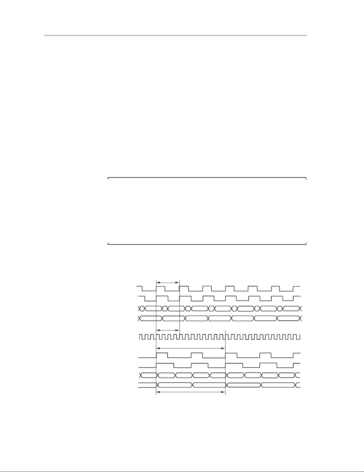
Description
7.1 Description
In order to understand—and better make use of—the MSC1210, it is necessary to understand some underlying information concerning timing.
The MSC1210 operates with timing derived from an external crystal or a clock
signal generated by some other system. A crystal is a mechanical oscillator
that allows an electronic oscillator to run at a very precisely known frequency .
One can find crystals of virtually any frequency depending on the application
requirements. When using an MSC1210, a common crystal frequency is
11.0592MHz due to baud rate accuracy considerations.
Microcontrollers (and many other electrical systems) use their oscillators to
synchronize operations. The MSC1210 uses its crystal or clock for precisely
that—to synchronize its internal operation. The MSC1210 operates using
what are called instruction cycles. A single instruction cycle is the minimum
amount of time in which a single MSC1210 instruction can be executed, although many instructions take multiple cycles.
Note:
A standard 8052 executes an instruction in 12 clock cycles rather than 4, as
shown in Figure 7−1. This means that, with no program changes, an
MSC1210 will execute code approximately three times faster than the same
program run under a traditional 8052. It also means that programs written for
a standard 8052 may have to be modified if they depend on certain
instructions executing in a certain amount of time. The fact that the MSC1210
executes an instruction in four cycles is not configurable.
Figure 7−1.Standard 8051 Timing.
ALE
PSEN
AD0−AD7
PORT2
XTAL1
ALE
PSEN
AD0−AD7
PORT2
Single−Byte
Single−Cycle
Instruction
4 Cycles
S in gle−B yt e S in g le
In str u ctio n
12 Cycles
−Cycle
7-2
Page 67

Description
An instruction cycle is, in reality, four clock cycles. That is to sa y, if an instruction takes one instruction cycle to execute, it will take four clocks from a crystal
or oscillator to execute. Using the maximum crystal frequency of 33MHz, the
crystal oscillates 33 000 000 times per second. Due to one instruction cycle
being four clock cycles, the MSC1210 can execute the following number of instruction cycles per second:
33 000 000 / 4 = 8 250 000
This means that the MSC1210 can execute 8 250 000 single-cycle instructions
per second.
It is i mportant t o e mphasize t hat n ot a ll i nstructions e xecute i n t he s ame a mount
of time. T he f astest i nstructions r equire o ne i nstruction c ycle ( four c lock c ycles),
many others r equire t wo i nstruction c ycles ( eight c lock c ycles), a nd t he t wo s low
math operations require four instruction cycles (16 clock cycles).
Due to all the instructions requiring different amounts of time to execute, a very
obvious question comes to mind: how can one keep track of time in a time-critical application if we have no reference to time in the outside world?
Luckily, the MSC1210 includes timers that allow us to time events with high
precision, which is the topic of the next chapter.
System Timing
7-3
Page 68

System Timers
7.2 System Timers
In addition to the standard 8052 timers to be described in Chapter 8, the
MSC1210 includes the following system timers, both of which are capable of
triggering an auxiliary interrupt (for more on interrupts, see chapter 10):
- Microseconds Timer: set via the USEC (FB
) SFR, and is used to configure
H
the flash writing timing and also used by the PWM module.
- Milliseconds Timer: set via the MSECH (FD
) and MSECL (FCH) SF Rs, a nd
H
is used as a base to configure the flash erase timing, as well as the milliseconds interrupt, and also as a base for the seconds interrupt and the watchdog
timer.
The MSC1210 timers are illustrated in Figure 7−2. The SYS Clock is the signal
that comes from the oscillator or other timing input. This signal is used as the
input for all of the part’s timing logic, including the following timing circuits:
- SPI I/O (chapter 13)
- PWM/Tone generation (chapter 11).
- Flash erase/write (chapter 15).
- Milliseconds/Seconds/Watchdog interrupts (chapter 7, 14).
- A/D conversion timing (chapter 12)
- Standard 8052 timers 0, 1, and 2 (chapter 8).
7-4
Page 69

Figure 7−2.MSC1210 Timing Chain and Clock Control
System Timers
Figure 7−3.SPI/PWM/Flash Write Timing
System Timing
7-5
Page 70

System Timers
7.2.1 Microseconds Timer
The microseconds timer is used by the MSC1210 in order to establish a 1µs
clock. This clock, in turn, is used by flash memory to establish timing for flash
writes, as well as by the PWM module.
The USEC (FB
ed by t he v alue o f t his S FR, p lus o ne, g enerates a 1 µs c lock. F or e xample, g iven
a system clock of 12.000MHz, USEC should be set to:
12 000 000/1 000 000 = 12 – 1 = 11.
Therefore, f or a 1 2.000MHz s ystem c lock, U SEC s hould b e s et t o 11 to g enerate
a 1µs clock.
In reality, the USEC SFR may be set to a value that produces a clock that is
something other than 1µs. This works fine as long as the other two timers that
depend on the USEC SFR are adjusted accordingly.
7.2.1.1 PWM Clock
The PWM module may use the microseconds timer as its input clock. By clearing SPDSEL (PWMCON.3), the input clock for the PWM module will be the microsecond timer. This creates a 1MHz input clock for the PWM module, assuming the microseconds timer is correctly configured to produce a 1µs clock.
In this case, the microseconds clock is further divided by the value contained
in the PWMHI/PWMLOW SFRs.
7.2.1.2 Flash Write Timing
The microseconds c lock i s f urther u sed t o e stablish t he f lash m emory write t iming.
The flash write t iming u ses t he m icrosecond clock a s a n i nput c lock a nd t hen f urther divides i t b y t he v alue o f F TCON[3:0] t o g enerate a f lash w rite c lock. T he f lash
write clock must be between 30µs and 40µs for flash writing t o operate p roperly.
) SFR s hould be set t o a v alue such that the s ystem c lock d ivid-
H
Specifically, FTCON[3:0] + 1, multiplied by five, multiplied by the frequency of the
microsecond clock, should produce an appropriate flash w rite timer ( 30µs t o 40µs).
Assuming USEC is set to generate a correct 1µs clock, FTCON[3:0] should be
set to 5, 6, or 7. If FTCON[3:0] is 6, then (6 + 1) S 5 = 35µs, which is right in the
middle of the expected range.
7.2.2 Milliseconds Timer
The milliseconds timer is used by the MSC1210 in order to establish a millisecond clock. This clock, in turn, is used as a base for establishing flash erase timing, the milliseconds interrupt, the seconds interrupt, and to establish timing
for the watchdog timer.
7-6
Page 71

Figure 7−4.System Timing Interrupt Control
The MSECH (FDH) and MSECL (FCH) SFRs should be se t to a value s uch that
the system clock divided b y t he v alue o f t hese S FRs, plus one, generates a 1ms
clock. For e xample, g iven a s ystem c lock o f 1 2.000MHz, MSECH/MSECL s hould
be set t o 1 2 000 000 / 1 000 = 1 2 0 00 – 1 = 11 999. Thus, f or a 1 2.000MHz s ystem
clock, MSECH/MSECL should be set to 11 999 to generate a 1ms clock.
System Timers
In reality, the MSECH/MSECL SFRs may be set to a value that produces a
clock that is something other than 1ms. This works fine, as long as the other
timers that depend on the MSECH/MSECL SFR are adjusted accordingly.
7.2.2.1 Milliseconds Auxiliary Interrupt
The milliseconds interrupt is one of the auxiliary interrupts that may be used
by the user program. The milliseconds auxiliary interrupt is enabled by setting
EMSEC (AIE.4) and enabling auxiliary interrupts via the EAI (EICON.5) bit.
The frequency at which the milliseconds interrupt will be triggered is controlled
by the value written to the MSINT (FA
When enabled, a millisecond a uxiliary interrupt will b e triggered after M SINT + 1 ms,
assuming that MSECH/MSECL have been configured to produce a correct
milliseconds clock. The value written to the MSINT SFR is a value between 0 and
127, meaning that the milliseconds interrupt may be triggered every 1ms to 128ms
(assuming a correct milliseconds clock).
For example, given an accurate milliseconds clock, setting MSINT to 5 would
produce a milliseconds auxiliary interrupt every 6ms.
Bit 7 of MSINT, when written, indicates whether the MSINT value being written
should be written immediately , or if it should be written after the current MSINT
count has expired. If bit 7 is set, MSINT will immediately be updated with the
new value; if it is clear, MSINT will be updated with the new value as soon as
the current milliseconds count has expired.
) SFR.
H
System Timing
7-7
Page 72

System Timers
7.2.2.2 One Hundred Millisecond Clock
The one hundred millisecond clock is used by the MSC1210 in order to establish a 10Hz clock. This clock is not directly outputted by the MSC1210; it is used
as the input into the seconds auxiliary interrupt and also is used by the watchdog timer. The 100ms clock uses the output of the millisecond clock (MSECH/
MSECL) as an input, so its correct operation assumes that the millisecond
clock has been set to a value that in fact generates a millisecond clock.
The HMSEC (FE
amount to 100ms (1/10th of a second), less 1. Therefore, assuming the millisecond clock is correctly configured to generate a 1kHz clock, HMSEC would
be set to 99 (decimal) in order to generate an accurate, 100ms clock.
7.2.2.3 Seconds Auxiliary Interrupt
The seconds auxiliary interrupt is one of the auxiliary interrupts that may be
used by the user program. The seconds auxiliary interrupt is enabled by setting ESEC (AIE.7) and enabling auxiliary interrupts via the EAI (EICON.5) bit.
The frequency at which the seconds interrupt will be triggered is controlled by
the value written to the SECINT (F9
When enabled, a seconds auxiliary interrupt will be triggered after
SECINT + 100ms, assuming the MSECH/MSECL and HMSEC SFRs have
been configured to produce a correct 100ms clock. The value written to the
SECINT SFR is between 0 and 127, meaning that the milliseconds interrupt
may be triggered every 100ms to 12.8 seconds (assuming a correct 100ms
clock).
For example, given an accurate 100ms clock, setting SECINT to 15 would
produce a seconds auxiliary interrupt every 1.6 seconds.
Bit 7 of SECINT, when written, indicates whether the SECINT value being
written should be written immediately, or if it should be written after the current
SECINT count has expired. If bit 7 is set, SECINT will immediately be updated
with the new value; if it is clear , SECINT will be updated with the new value as
soon as the current seconds count has expired.
) SFR is used to indicate how many millisecond clocks
H
) SFR.
H
7.2.2.4 Watchdog Timer
The functioning of the watchdog timer is fully described in section 14.3. However, it is important to keep in mind that the watchdog timer is dependent on
the 100ms timer. The length of the watchdog timer is directly dependent on the
100ms timer being configured to a reasonable value because the watchdog
timer frequency is configured in WDTCON (FF
7-8
) using units of HMSEC.
H
Page 73
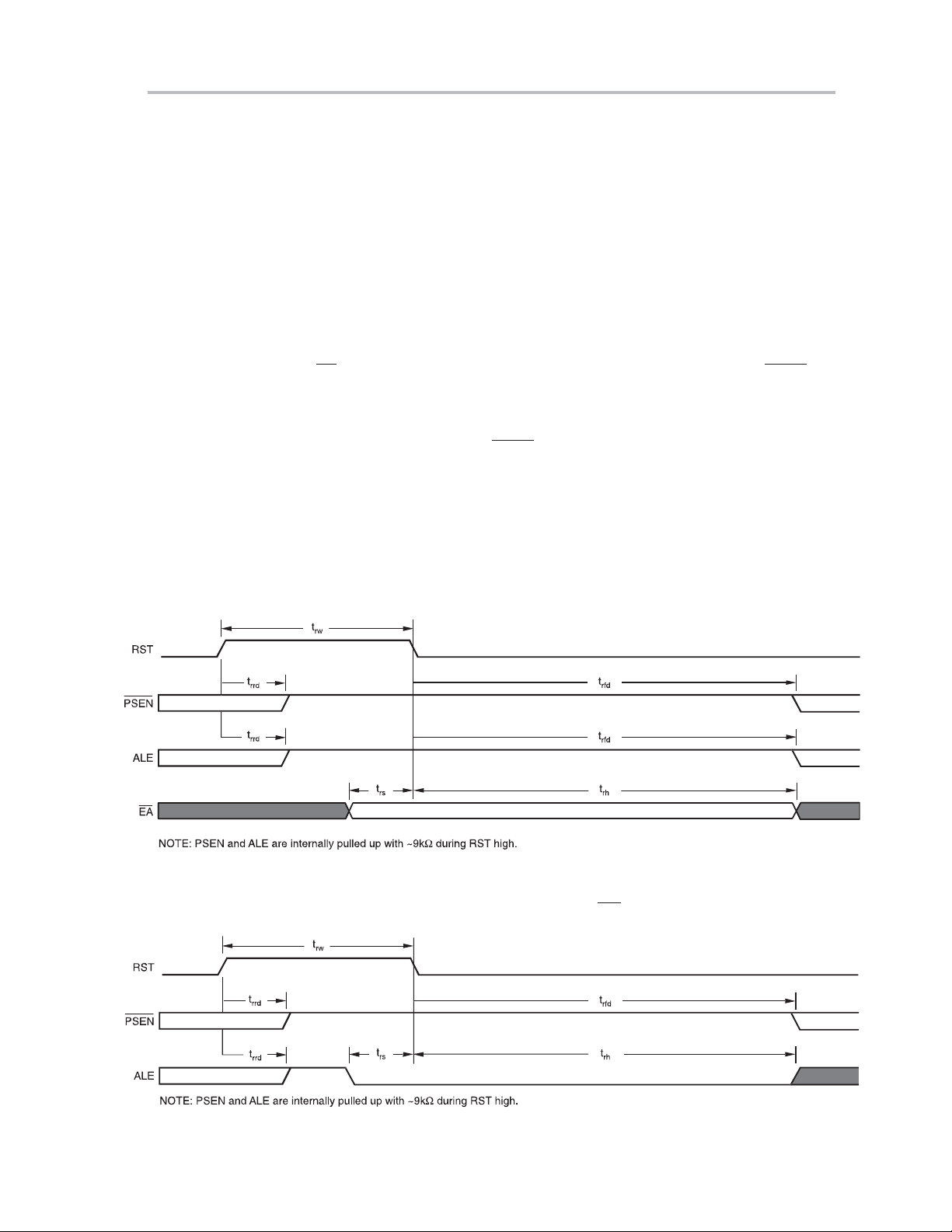
7.3 Startup Timing
Startup Timing
When power is turned on, or a reset is initiated, a power-on delay circuit is implemented with a 17-bit counter to guarantee that the power supply has
reached a certain level, and the oscillator is stable. The delay introduced by
this counter is:
17
− 1) S (1/24) S 10
24MHz System clock: (2
1MHz System clock: (2
17
− 1) S 10
−6
= 0.131071s
7.3.1 Normal-Mode Power-On Reset Timing
EA is sampled during power-on reset for code security purposes. PSEN and
ALE are internally pulled up during reset for serial and parallel flash programming mode detection.
After the reset sequence, PSEN
and ALE signals are driven by the CPU, and
the internal pull up resistors are removed for saving power.
7.3.2 Flash Programming Mode Power-On Reset Timing
EA is ignored for serial and parallel flash programming operations.
Figure 7−5.Reset Timing
−6
= 0.005461s
Figure 7−6.Parallel Flash Programming Power-On Timing (EA is ignored)
System Timing
7-9
Page 74

Startup Timing
Figure 7−7.Serial Flash Programming Power-On Timing (EA is ignored)
Table 7−1.Signal Definitions for Reset Timing Diagrams
Symbol Parameter Min Max Unit
t
rw
t
rrd
t
rfd
t
rs
t
rh
Notes: 1) t
RST Width 10 t
RST rise to PSEN ALE internal pull high — 5 µs
RST falling to PSEN and ALE start — (217+512) t
Input signal to RST falling setup time t
RST falling to input signal hold time (217+512) t
is the Xtal clock period.
CLK
CLK
CLK
(1)
(1)
CLK
(1)
— ns
CLK
(1)
ns
— ns
— ns
7-10
Page 75

Chapter 8
Chapter 8 describes the timers of the MSC1210 ADC.
Topic Page
8.1 Description 8-2. . . . . . . . . . . . . . . . . . . . . . . . . . . . . . . . . . . . . . . . . . . . . . . . . . .
8.2 How Does a Timer Count? 8-2. . . . . . . . . . . . . . . . . . . . . . . . . . . . . . . . . . . . .
8.3 Using Timers to Measure Time 8-2. . . . . . . . . . . . . . . . . . . . . . . . . . . . . . . . .
8.4 Using Timers as Event Counters 8-12. . . . . . . . . . . . . . . . . . . . . . . . . . . . . .
8.5 Using Timer 2 8-13. . . . . . . . . . . . . . . . . . . . . . . . . . . . . . . . . . . . . . . . . . . . . . . .
Timers
8-1
Page 76

Description
8.1 Description
The MSC1210 comes equipped with three standard timer/counters, all of
which may be controlled, set, read, and configured individually. The
timer/counters have three general functions:
1) Keeping time and/or calculating the amount of time between events
2) Counting the events themselves
3) Generating baud rates for the serial port
The uses of the three timer/counters are distinct, so we will talk about each of
them separately. The first two uses will be discussed in this chapter, whereas
the use of timers for baud rate generation will be discussed in the Chapter 9,
Serial Communication.
8.2 How Does a Timer Count?
The answer to this question is very simple: a timer always counts up. It does
not matter whether the timer is being used as a timer, a counter, or a baud rate
generator. A timer is always incremented by the microcontroller.
8.3 Using Timers to Measure Time
Obviously, one of the primary uses of timers is to measure time. We will discuss
this use of timers first and will subsequently discuss the use of timers to count
events. When a timer is used to measure time, it is also called an interval timer ,
because it is measuring the time of the interval between two events.
8.3.1 How Long Does a Timer Take to Count?
Before continuing, it is worth mentioning that when a timer is in interval timer
mode (as opposed to event counter mode) and correctly configured, the timer
will increment by one on each instruction cycle. Therefore, a running timer in
the MSC1210 will be incremented:
33 000 000 / 4 = 8 250 000 times per second
However, to maintain compatibility with existing 8052 code, the default mode
for the MSC1210 timers is to increment by one every three instruction cycles
(i.e., operate as if the timer increments every 12 clocks). Thus, a running timer
can be configured to be incremented:
33 000 000 / 12 = 2 750 000 times per second
Using the first option, which increments the timer every four clocks, allows the
user program to obtain three times higher precision than would be available
by the default mode just explained. Whether the timers are incremented every
four or 12 clocks is controlled by the CKCON SFR.
8-2
Page 77

SFR 8E
Using Timers to Measure Time
The individual bits of TMOD have the following functions:
7 6 5 4 3 2 1 0 Reset Value
H
0 0 T2M T1M T0M MD2 MD1 MD0 01
H
T2M (bit 5)—Timer 2 Clock Select. This bit controls the division of the system
clock that drives Timer 2. This bit has no effect when the timer is in baud rate
generator or clock output modes. Clearing this bit to 0 maintains 80C32 compatibility. This bit has no effect on instruction cycle timing.
0: Timer 2 uses a divide by 12 of the crystal frequency.
1: Timer 2 uses a divide by 4 of the crystal frequency.
T1M (bit 4)—Timer 1 Clock Select. This bit controls the division of the system
clock that drives Timer 1. Clearing this bit to 0 maintains 8051 compatibility.
This bit has no effect on instruction cycle timing.
0: Timer 1 uses a divide by 12 of the crystal frequency.
1: Timer 1 uses a divide by 4 of the crystal frequency.
T0M (bit 3)—Timer 0 Clock Select. This bit controls the division of the system
clock that drives Timer 0. Clearing this bit to 0 maintains 8051 compatibility.
This bit has no effect on instruction cycle timing.
0: Timer 0 uses a divide by 12 of the crystal frequency.
1: Timer 0 uses a divide by 4 of the crystal frequency.
MD2, MD1, MD0 (bits 2-0)—Stretch MOVX Select 2−0. These bits select the
time by which external MOVX cycles are to be stretched. This allows slower
memory or peripherals to be accessed without using ports or manual software
intervention. The RD
or WR strobe will be stretched by the specified interval,
which will be transparent to the software except for the increased time to execute the MOVX instruction. All internal MOVX instructions on devices containing MOVX SRAM are performed at the 2 instruction cycle rate.
RD or WR
Strobe
Stretch
MD2 MD1 MD0
0 0 0 0 2 Instruction Cycles 2 0.167
0 0 1 1 3 Instruction Cycles
0 1 0 2 4 Instruction Cycles 8 0.667
0 1 1 3 5 Instruction Cycles 12 1.000
1 0 0 4 6 Instruction Cycles 16 1.333
1 0 1 5 7 Instruction Cycles 20 1.667
1 1 0 6 8 Instruction Cycles 24 2.000
1 1 1 7 9 Instruction Cycles 28 2.333
Value
MOVX Duration
(default)
Width
(SYS CLKs)
4 0.333
RD or WR
Strobe
Width (µs)
at 12MHz
Timers
8-3
Page 78

Using Timers to Measure Time
Unlike instructions—some of which require one instruction cycle, others 2, and
others 4—the t i m e r s a r e c o n s i s t e n t . T h e y w i l l always be incremented once every 12 (or four) clocks. Therefore, if a timer has counted from 0 to 55 000 you
may calculate:
55 000 / 2 750 000 = 0.020 seconds (f
55 000 / 8 250 000 = 0.007 seconds (f
The trade off in using f
and (2) resolution. With a 33MHz external clock, the resolution of f
per increment, and the resolution of f
Thus, we now have a system that measures time. All we need to review is how
to control t he t imers a nd i nitialize t hem t o p rovide u s w ith t he i nformation n eeded.
8.3.2 Timer SFRs
As mentioned before, the MSC1210 has three standard timers. Two of these
timers work in essentially the same way. One timer is Timer 0 and the other
is Timer 1. The two timers share two SFRs (TMOD and TCON) which control
the timers, and each timer also has two SFRs dedicated solely to maintaining
the value of the timer itself (TH0/TL0 and TH1/TL1). The third timer (Timer 2)
functions somewhat differently and will be explained separately.
The SFRs used to control and manipulate the first two timers are presented
in the Table 8−1.
Table 8−1.Timer Conrol SFRs.
osc
/12 or f
/12) or
osc
/4)
osc
/4 as the clock source is (1) code compatibility
osc
/12 = 364ns
osc
/4 is 121ns per increment.
osc
SFR Name Description SFR Address Bit Addressable?
TH0 Timer 0 high byte 8C
TL0 Timer 0 low byte 8A
TH1 Timer 1 high byte 8D
TL1 Timer 1 low byte 8B
TCON Timer control 88
TMOD Timer mode 89
H
H
H
H
H
H
No
No
No
No
Yes
No
Timer 0 has two SFRs dedicated exclusively to itself: TH0 and TL0. TL0 is the
low byte of the value of the timer, while TH0 is the high byte of the value of the
timer. That is to say, when Timer 0 has a value of 0, both TH0 and TL0 will contain 0. When Timer 0 has the value 1000, TH0 will hold the high byte of the value (3 decimal) and TL0 will contain the low byte of the value (232 decimal).
Reviewing low/high byte notation, recall that you must multiply the high byte
by 256 and add the low byte to calculate the final value. In this case:
(TH0 S 256) + TL0 = 1000
(3 S 256) + 232 = 1000
Timer 1 works the exact same way, but its SFRs are TH1 and TL1.
8-4
Page 79

8.3.3 TMOD SFR
7 6 5 4 3 2 1 0
SFR 89
H
GATE C/T M1 M0 GATE C/T M1 M0 00
Using Timers to Measure Time
It is apparent t hat the m aximum v alue a t imer m ay h ave i s 6 5,535 b ecause t here
are only t wo b ytes d evoted t o t he v alue o f e ach t imer. If a t imer c ontains t he v alue
65,535 and is subsequently incremented, it will reset—or overflow—back to 0.
The TMOD SFR i s us ed t o control t he m ode o f o peration o f b oth t imers. E ach b it
of the SFR gives the microcontroller specific information concerning how to run
a timer. The high four bits (bits 4 through 7) relate to Timer 1, whereas the low
four bits (bits 0 through 3) perform the exact same functions, but for Timer 0.
The individual bits of TMOD have the following functions:
TIMER 1 TIMER 0
Reset Value
H
GATE (bit 7)—Timer 1 Gate Control. This bit enables/disables the ability of
Timer 1 to increment.
0: Timer 1 will clock when TR1 = 1, regardless of the state of pin INT1
1: Timer 1 will clock only when TR1 = 1 and pin INT1
C/T
(bit 6)—Timer 1 Counter/Timer Select.
= 1.
.
0: Timer is incremented by internal clocks.
1: Timer is incremented by pulses on pin T1 when TR1 (TCON.6, SFR 88
) is 1.
H
M1, M0 (bits 5-4)—Timer 1 Mode Select. These bits select the operating
mode of Timer 1.
M1 M0 Mode
0 0 Mode 0: 8-bit counter with 5-bit prescale.
0 1 Mode 1: 16 bits.
1 0 Mode 2: 8-bit counter with auto-reload.
1 1 Mode 3: Timer 1 is halted, but holds its count.
GATE (bit 3)—Timer 0 Gate Control. This bit enables/disables the ability of
Timer 0 to increment.
0: Timer 0 will clock when TR0 = 1, regardless of the state of pin INT0
(software
control).
1: Timer 0 will clock only when TR0 = 1 and pin INT0
C/T
(bit 2)—Timer 0 Counter/Timer Select.
= 1 (hardware control).
0: Timer is incremented by internal clocks.
1: Timer is incremented by pulses on pin T0 when TR0 (TCON.4, SFR 88H) is 1.
M1, M0 (bits 1-0) Timer 0 Mode Select. These bits select the operating mode
of Timer 0.
M1 M0 Mode
0 0 Mode 0: 8-bit counter with 5-bit prescale.
0 1 Mode 1: 16 bits.
1 0 Mode 2: 8-bit counter with auto-reload.
1 1 Mode 3: Timer 1 is halted, but holds its count.
Timers
8-5
Page 80
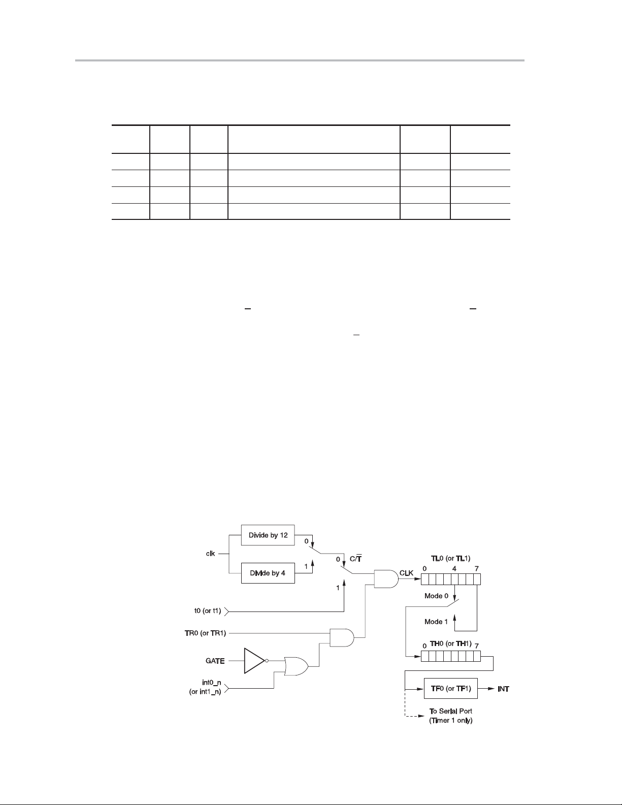
Using Timers to Measure Time
As is shown in the previous chart, four bits (two for each timer) are used to
specify a mode of operation. The modes of operation are shown in Table 8−2.
Table 8−2.Timer Modes and Usage
TxM1 TxM0 Timer
Mode
0 0 0 13-bit timer/counter Y Y
0 1 1 16-bit timer/counter Y Y
1 0 2 8-bit timer/counter with auto-reload Y Y
1 1 3 Two 8-bit counters (split timer mode) N Y
Description of Timer Mode Timer 1 Timer 0
The TMOD.GATE bit controls gating of the timer/counter. If TMOD.GATE is
cleared, the timer/counter increments only if TCON.TRx is set. If TMOD.GATE
is set, the timer/counter increments only if TCON.TRx is set and the corresponding INTx pin is held high. This feature can be used for pulse width measurements.
The TMOD.CT
the timer/counter register is incremented on either f
the state of CKCON.TxM ). If TMOD.CT
cremented by the Tx pin.
8.3.3.1 13-Bit Time Mode (mode 0)
Timer mode 0 is a 13-bit timer. This is a relic that was kept around in the 8052
(and subsequently MSC1210) to maintain compatibility with its predecessor,
the 8048. The 13-bit timer mode is not normally used in new development.
bit selects counter or timer operation. If TMOD.CT is cleared,
osc
/4 or f
/12 (based on
osc
is set, the timer/counter register is in-
In this mode, the timer/counter uses five bits of the TLx register and all eight
bits of the THx register for the 13-bit register. Therefore, the upper three bits
of TLx must be masked if they are used by software. When the timer/counter
rolls over on a transition from 01FFF
(TCON.TFx).
Figure 8−1.Timer 0/1 Block Diagram for Modes 0 and 1
, the timer/counter interrupt flag is set
H
8-6
Page 81

When the timer is in 13-bit mode, TLx will count from 0 to 31. When TLx is incremented from 31, it will roll over to 0 and overflow into THx, thus incrementing it. Therfore, only 13 bits of the two timer bytes are being used: bits 0 to 4
of TLx, and bits 0 to 7 of THx. This also means the timer can only contain 8192
values. If you set a 13-bit timer to 0, it overflows back to zero 8192 instruction
cycles later.
There is very little reason to use this mode and it is only mentioned so there
will be no surprise if ever analyzing archaic code that has been passed down
through the generations.
8.3.3.2 16-Bit Time Mode (mode 1)
Mode 1 operates in the same manner as mode 0, except Timer 0 or Timer 1
is configured as a 16-bit timer/counter. The timer/counter uses all 8 bits of both
the TLx register and THx register for the 16-bit register.
Using Timers to Measure Time
When the timer/counter rolls o ver o n a transition from 0FFFF
interrupt flag is set (TCON.TFx).
Timer mode 1 is a 16-bit timer. This is a very commonly used mode. It functions
just like 13-bit mode, except that all 16 bits are used.
TLx is incremented from 0 to 255. When TLx is incremented from 255, it resets
to 0 and causes THx to be incremented by 1. The timer may contain up to
65 536 distinct values because this is a full 16-bit timer. If a 16-bit timer is set
to 0, it will overflow back to 0 after 65 536 machine cycles.
8.3.3.3 8-Bit Auto-Reload Time Mode (mode 2)
Timer mode 2 is an 8-bit auto-reload mode. When a timer is in mode 2, THx
holds the reload value and TLx is the timer itself.
TLx starts counting up. When TLx reaches 255 and is subsequently incremented instead of resetting to 0 (as in the case of modes 0 and 1), it will be reset
to the value stored in THx.
For example, TH0 holds the value FD
Table 8−3 shows what would occur if the values of TH0 and TL0 are viewed
for a few machine cycles.
, the timer/counter
H
and TL0 holds the value FEH.
H
Table 8−3.Example of 8-Bit Auto-Reload
Instruction
Cycle
1 FD
2 FD
3 FD
4 FD
5 FD
6 FD
7 FD
TH0
Value
H
H
H
H
H
H
H
TL0
Value
FE
H
FF
H
FD
H
FE
H
FF
H
FD
H
FE
H
Timers
8-7
Page 82

Using Timers to Measure Time
As shown, the value of TH0 never changed. In fact, when mode 2 is used, THx
is almost always set to a known value and TLx is the SFR that is constantly
incremented. THx is initialized once, and then left unchanged.
The benefit of auto-reload mode is that, perhaps, the timer may need to always
have a value from 200 to 255. When using mode 0 or 1, the code would have to
be checked to see if the t imer had o verflowed and, i f so, t he timer r eset to 2 00. T his
takes precious amounts of execution time to check the value and/or reload it.
When mode 2 is used, the microcontroller takes care of this. Once a timer has
been configured in mode 2, it does not have to be checked to see if the timer
has overflowed, nor does the value need to be reset—the microcontroller
hardware will do it all.
The auto-reload mode is very commonly used for establishing a baud rate,
which will be discussed further in Chapter 9, Serial Communications.
8.3.3.4 Split-Timer Mode (mode 3)
Timer mode 3 is a split-timer mode. When Timer 0 is placed in mode 3, it essentially becomes two separate 8-bit timers. That is to say, T imer 0 is TL0 and Timer 1 is TH0. Both timers count from 0 to 255 and overflow back to 0. All the bits
that are related to Timer 1 will now be tied to TH0, and all the bits related to
Timer 0 will be tied to TL0.
While Timer 0 is in split mode, the real Timer 1 (i.e. TH1 and TL1) can be put
into modes 0, 1, or 2 normally. However, the real T imer 1 may not be started
or stopped, because the bits that do that are now linked to TH0. The real Timer
1, in this case, will be incremented every machine cycle no matter what. The
real Timer 1 may be stopped by setting it to mode 3.
The only real use of note in using split-timer mode is if two separate timers are
needed along with a baud rate generator. In such a case, use the real Timer
1 as a baud rate generator, and use TH0/TL0 as two separate timers.
8.3.4 TCON SFR
Finally, there is one more SFR that controls the two timers and provides valuable information about them. The TCON SFR has the structure described in
Table 8−4.
Table 8−4.TCON (88H) SFR
Bit Name Bit Address Explanation of Function Timer
Timer 1 overflow. This bit is set by the microcontroller
7 TF1 8F
6 TR1 8E
5 TF0 8D
4 TR0 8C
H
H
H
H
when Timer 1 overflows.
Timer 1 run. When this bit is set, Timer 1 is turned on.
When this bit is clear, Timer 1 is off.
Timer 0 overflow. This bit is set by the microcontroller
when Timer 0 overflows.
Timer 0 run. When this bit is set, Timer 0 is turned on.
When this bit is clear, Timer 0 is off.
1
1
0
0
8-8
Page 83

So far, only four of the eight bits have been defined. That is because the other
four bits of the SFR do not have anything to do with timers—they have to do
with interrupts and they will be discussed in Chapter 10, Interrupts.
Table 8−4 contains the bit address column because this SFR is bit-addressable. That means in order to set bit TF1, which is the highest bit of TCON, you
execute the command:
MOV TCON, #80h
However, because this SFR is bit-addressable, you can execute the command:
SETB TF1
This has the benefit of setting the high bit of TCON without changing the value
of any of the other bits of the SFR. Usually, when starting or stopping a timer,
the other values in TCON should not be modified, so take advantage of the fact
that the SFR is bit-addressable.
8.3.5 Initializing a Timer
After discussing the timer-related SFRs, it is time to write code that initializes
the timer and starts it running. As shown previously, the timer mode should be
decided upon. In this case, a 16-bit timer that runs continuously will be used;
that is to say, it is not dependent on any external pins.
Using Timers to Measure Time
We must first initialize the TMOD SFR. When working with Timer 0, the low four
bits of TMOD will be used. The first two bits, GA TE0 and CT
cause the timer needs to be independent of the external pins. 16-bit mode is
timer mode 1, so T0M1 must be cleared and T0M0 must be set. Effectively, bit
0 of TMOD is the only bit that should be turned on. Therefore, to initialize the
timer, execute the instruction:
MOV TMOD,#01h
Timer 0 is now in 16-bit timer mode, however, the timer is not running. To start
the timer running, set the TR0 bit by executing the instruction:
SETB TR0
Upon executing these two instructions, Timer 0 will immediately begin counting, being incremented once every instruction cycle (every 12 crystal pulses).
8.3.6 Reading the Timer
There are two common ways of reading the value of a 16-bit timer; which one
is used depends on the specific application. The actual value of the timer may
be read as a 16−bit number, or the timer may be detected when overflowed.
8.3.6.1 Reading the Value of a Timer
0 are both 0, be-
If the timer is in 8-bit mode—that is, either 8-bit auto-reload mode, or in splittimer mode—reading the value of the timer is simple. Just read the 1-byte value of the timer and that is it.
Timers
8-9
Page 84

Using Timers to Measure Time
However, when dealing with a 13-bit or 16-bit timer, the chore is a little more
complicated. Consider what happens when the low byte of the timer is read
as 255, then the high byte of the timer is read as 15. In this case, what actually
happens is that the timer value is 14/255 (high byte 14, low byte 255) but the
readout is 15/255. The reason for this is because the low byte was read as 255.
However, when the next instruction is executed, enough time passes for the
timer to increment again, which rolls the value over from 14/255 to 15/0. In the
process, the timer is read as being 15/255 instead of 14/255. Obviously, this
is a problem.
The solution is not complicated. Read the high byte of the timer, then read the
low byte, then read the high byte again. If the high byte read the second time
is not the same as the high byte read the first time you repeat the cycle. In code,
this would appear as:
REPEAT:
MOV A,TH0
MOV R0,TL0
CJNE A,TH0,REPEAT
...
In this case, the accumulator is loaded with the high byte of Timer 0. Then R0
is loaded with the low byte of Timer 0. Finally, the high byte we read out of T imer
0—which is now stored in the accumulator—is checked to see if it is the same
as the current Timer 0 high byte. If it is not, that means it just rolled over and
the timer value must be reread, which is done by going back to REPEAT. When
the loop exits, the low byte of the timer is in R0 and the high byte is in the accumulator.
Another much simpler alternative is to simply turn off the timer run bit (i.e. CLR
TR0), read the timer value, and then turn on the timer run bit (i.e. SETB TR0).
In this case, the timer is not running, so no special tricks are necessary. Of
course, this implies that the timer will be stopped for a few instruction cycles.
Whether or not this is tolerable depends on the specific application.
8.3.6.2 Detecting Timer Overflow
Often it is only necessary to know that the timer has reset to 0. That is to say,
there is no particular interest in the value of the timer, but rather an interest in
knowing when the timer has overflowed back to 0.
Whenever a timer overflows from its highest value back to 0, the
microcontroller automatically sets the TFx bit in the TCON register. This is
useful because, rather than checking the exact value of the timer , you can just
check if the TFx bit is set. If the TF0 bit is set, it means that Timer 0 has
overflowed; if TF1 is set, it means that Timer 1 has overflowed.
8-10
Page 85

Using Timers to Measure Time
This approach can be used to cause the program to execute a fixed delay. As
shown earlier, w e calculated that it takes the 8051 1/20th of a second to count
from 0 to 46 080. However, the TFx flag is set when the timer overflows back
to 0.
Therefore, to use the TFx flag to indicate when 1/20th of a second has passed,
the timer must be set initially to 65 536 less 46 080, or 19 456. If the timer is
set to 19 456, 1/20th of a second later the timer will overflow. Thus, the following code will execute a pause of 1/20th of a second:
MOV TH0,#76 ;High byte of 19,456 (76 * 256 = 19,456)
MOV TL0,#00 ;Low byte of 19,456 (19,456 + 0 = 19,456)
MOV TMOD,#01 ;Put Timer 0 in 16−bit mode
CLR TF0 ;Make sure TF0 bit is clear initially
SETB TR0 ;Make Timer 0 start counting
JNB TF0,$ ;If TF0 is not set, jump back to this same
;instruction
In the above code, the first two lines initialize the Timer 0 starting value to
19 456. The next two instructions configure Timer 0 and turn it on. Finally, the
last instruction (JNB TF0,$) reads: jump back to the same instruction if TF0 is
not set. The $ operand means, in most assemblers, the address of the current
instruction.
As long as the timer has not overflowed and the TF0 bit has not been set, the
program will keep executing this same instruction. After 1/20th of a second,
Timer 0 overflows, sets the TF0 bit, and program execution then breaks out
of the loop.
8.3.7 Timing the Length of Events
The MSC1210 provides another useful method to time the length of events.
For example, in order to save electricity in the office, a light switch is measured
to see how long it is turned on each day. When the light is turned on, time must
be measured; when the light is turned off, time is not measured. One option
is to connect the light switch to one of the pins, constantly read the pin, and
turn the timer on or off based on the state of that pin. Although this method
works well, the MSC1210 provides an easier way of accomplishing this.
Looking again at the TMOD SFR, there is a bit called GATE0. So far, this bit
has always been cleared because the timer is run regardless of the state of
the external pins. However, now it would be nice if an external pin could control
whether the timer was running or not. It can.
Simply connect the light switch to pin INT0
bit GA TE0. When GATE0 is set, Timer 0 will only run if P3.2 is high. When P3.2
is low (i.e., the light switch is off) the timer will automatically be stopped.
(P3.2) on the MSC1210 and set the
Thus, with no control code whatsoever, the external pin P3.2 can control
whether or not the timer is running.
Timers
8-11
Page 86

Using Timers as Event Counters
8.4 Using Timers as Event Counters
We have discussed how a timer can be used for the obvious purpose of keeping track of time. However, the MSC1210 also allows the use of timers to count
events.
This can be useful in many applications. For example, a sensor is placed
across a road that would send a pulse every time a car passes over it. This
could be used to determine the volume of traffic on the road. The sensor is attached to one of the MSC1210 I/O lines and constantly monitored, detecting
when it pulses high, and the counter incremented when it goes back to a low
state. This is not terribly difficult, but requires some code. If the sensor is
hooked to P1.0, the code to count passing cars would look something like this:
JNB P1.0,$ ;If a car hasn’t raised the signal,
;keep waiting
JB P1.0,$ ;The line is high, car is on the sensor
;right now
INC COUNTER ;The car has passed completely, so we count it
As shown, it is only three lines of code. However, what if other processing
needs to be done at the same time? The program cannot be stuck in the JNB
P1.0,$ loop waiting for a car to pass if it needs to be doing other things. What
if the program is doing other things when a car passes over? It is possible that
the car will raise the signal and the signal will fall low again before the program
checks the line status; this would result in the car not being counted. Of course,
there are ways to get around even this limitation, but the code quickly becomes
big, complex, and ugly.
Luckily, the MSC1210 provides a way to use the timers to count events. It is
painfully easy. Only one additional bit has to be configured.
Timer 0 can be used to count the number of cars that pass. In the bit table for
the TCON SFR, there is a bit called C/T
0—it is bit 2 (TCON.2). Reviewing the
explanation of the bit, we see that if the bit is clear , Timer 0 will be incremented
every instruction cycle. This is what has already been used to measure time.
0 is set, however, Timer 0 will monitor the P3.4 line. Instead of being in-
If C/T
cremented every machine cycle, Timer 0 will count events on the P3.4 line. So
in this case, simply connect the sensor to P3.4 and let the 8052 do the work.
Then, when the number of how many cars have passed is desired, just read
the value of Timer 0—the value of Timer 0 will be the number of cars that have
passed.
So what exactly is an event? What does Timer 0 actually count? Speaking at
the electrical level, the MSC1210 counts 1−0 transitions on the P3.4 line. This
means that when a car first runs over the sensor, it raises the input to a high
(1) condition. At that point, the MSC1210 does not count anything because this
is a 0−1 transition. However, when the car has passed, the sensor falls back
to a low (“0”) state. This is a 1−0 transition and at that instant the counter is
incremented by 1.
8-12
Page 87

8.5 Using Timer 2
8.5.1 T2CON SFR
7 6 5 4 3 2 1 0 Reset Value
SFR C8
H
TF2 EXF2 RCLK TCLK EXEN2 TR2 C/T CP/RL2 00
Using Timer 2
It is important to note that the MSC1210 checks the P3.4 line each instruction
cycle (4 clock cycles). This means that if P3.4 is low, goes high, and goes back
low in 3 clock cycles, it will probably not be detected by the MSC1210. This also
means the MSC1210 e vent c ounter i s o nly c apable o f c ounting e vents t hat o ccur
at a m aximum o f 1 /8th t he r ate o f t he c rystal f requency. That i s t o s ay, if the c rystal
frequency is 1 2.000MHz, i t c an c ount a maximum of 1 5 00 0 00 e vents p er s econd
(12.000MHz S 1/8 = 1 500 000). If the event being counted occurs more than
1 500 000 times per second, the MSC1210 will not be able to accurately count
the event without using additional external circuitry or a faster crystal.
The MSC1210 has a third timer, Timer 2, which functions slightly differently
than T imers 0 and 1 and, for that reason, we are addressing this third timer separately from the first two.
The operation of Timer 2 (T2) is controlled almost entirely by the T2CON SFR,
at address C8H. This SFR is bit-addressable because this SFR is evenly divisible by eight.
The individual bits of T2CON have the following functions:
H
TF2 (bit 7)—Timer 2 Overflow Flag. This flag will be set when Timer 2 overflows
from FFFF
. It must be c leared b y software. T F2 w ill only b e s et if R CLK a nd T CLK
H
are both cleared to 0. Writing a 1 to TF2 forces a Timer 2 interrupt if enabled.
EXF2 (bit 6) Timer 2 External Flag. A negative transition on the T2EX pin
(P1.1) will cause this flag to be set based on the EXEN2 (T2CON.3) bit. If set
by a negative transition, this flag must be cleared to 0 by software. Setting this
bit in software will force a timer interrupt, if enabled.
RCLK (bit 5)—Receive Clock Flag. This bit determines the serial Port 0 timebase when receiving data in serial modes 1 or 3.
0 = Timer 1 overflow is used to determine receiver baud rate for serial Port 0.
1 = Timer 2 overflow is used to determine receiver baud rate for serial Port 0.
Setting this bit will force T imer 2 into baud rate generation mode. The timer will
operate from a divide by 2 of the external clock.
TCLK (bit 4)—Transmit Clock Flag. This bit determines the serial Port 0 timer
base when transmitting data in serial modes 1 or 3.
0 = Timer 1 overflow is used to determine transmitter baud rate for serial Port 0.
1 = Timer 2 overflow is used to determine transmitter baud rate for serial Port 0.
Setting this bit will force T imer 2 into baud rate generation mode. The timer will
operate from a divide by 2 of the external clock.
EXEN2 (bit 3)—Timer 2 External Enable. This bit enables the capture/reload
function on the T 2EX p in i f Timer 2 is not g enerating b aud r ates f or t he s erial p ort.
0 = Timer 2 will ignore all external events at T2EX.
1 = Timer 2 will capture or reload a value if a negative transition is detected on
the T2EX pin.
Timers
8-13
Page 88

Using Timer 2
TR2 (bit 2)—Timer 1 Run Control. This bit enables/disables the operation of
Timer 2. Halting this timer will preserve the current count in TH2, TL2.
0 = Timer 2 is halted.
1 = Timer 2 is enabled.
C/T
(bit 1)—Counter/Timer Select. This bit determines whether Timer 2 will
function as a timer or counter. Independent of this bit, Timer 2 runs at 2 clocks
per tick when used in baud rate generator mode.
0 = Timer 2 functions as a timer. The speed of Timer 2 is determined by the
T2M bit (CKCON.5).
1 = Timer 2 will count negative transitions on the T2 pin (P1.0).
CP/RL2
(bit 0)—Capture/Reload Select. This bit determines whether the
capture or reload function will be used for Timer 2. If either RCLK or TCLK is
set, this bit will not function and the timer will function in an auto-reload mode
following each overflow.
0 = Auto-reloads will occur when Timer 2 overflows or a falling edge is detected
on T2EX if EXEN2 = 1.
1 = Timer 2 captures will occur when a falling edge is detected on T2EX if
EXEN2 = 1.
8.5.2 Timer 2 in Auto-Reload Mode
The first mode in which Timer 2 may be used is auto-reload. The auto-reload
mode functions just like Timer 0 and Timer 1 in auto-reload mode, except that
the Timer 2 auto-reload mode performs a full 16-bit reload (recall that Timer
0 and Timer 1 only have 8-bit reload values). When a reload occurs, the value
of TH2 is reloaded with the value contained in RCAP2H, and the value of TL2
is reloaded with the value contained in RCAP2L.
To operate Timer 2 in auto-reload mode, the CP/RL2 bit (T2CON.0) must be
clear. In this mode, Timer 2 (TH2/TL2) is reloaded with the reload value
(RCAP2H/RCAP2L) whenever Timer 2 overflows; that is to say, whenever
Timer 2 overflows from FFFF
the TF2 bit to be set, which causes an interrupt to be triggered (if T imer 2 interrupt is enabled). Note that TF2 will not be set on an overflow condition if either
RCLK or TCLK (T2CON.5 or T2CON.4) are set.
back to 0000H. An overflow of Timer 2 causes
H
8-14
Additionally, by also setting EXEN2 (T2CON.3), a reload will also occur whenever a 1−0 transition is detected on T2EX (P1.1). A reload that occurs as a result of such a transition causes the EXF2 (T2CON.6) flag to be set, triggering
a Timer 2 interrupt, if enabled.
Page 89

8.5.3 Timer 2 in Capture Mode
A new mode, specific to Timer 2, i s called capture mode. As the name implies,
this mode captures the value of T imer 2 (TH2 and TL2) into the capture SFRs
(RCAP2H and RCAP2L). To put Timer 2 in capture mode, CP/RL2 (T2CON.0)
and EXEN2 (T2CON.3) must be set.
When configured as mentioned above, a capture occurs whenever a 1-0 transition is detected on T2EX (P1.1). At the moment the transition is detected, the
current values of TH2 and TL2 is copied into RCAP2H and RCAP2L, respectively . A t the same time, the EXF2 (T2CON.6) bit is set, which triggers an interrupt, if Timer 2 interrupt is enabled.
Note:
Even in capture mode, an overflow of Timer 2 results in TF2 being set and
an interrupt being triggered.
Note:
Capture mode is an efficient way to measure the time between events. At the
moment that an event occurs, the current value of Timer 2 is copied into
RCAP2H/L. However , Timer 2 will not stop and an interrupt will be triggered.
Thus the interrupt routine must copy the value of RCAP2H/L to a temporary
holding variable without stopping Timer 2. When another capture occurs, t h e
interrupt can take the difference of the two values to determine the time transpired. Again, the main advantage is that Timer 2 does not need to be
stopped to have its value read, as is the case with Timer 0 and Timer 1.
Using Timer 2
Timers
8-15
Page 90

Using Timer 2
8.5.4 Timer 2 as a Baud Rate Generator
Timer 2 can be used as a baud rate generator. This is accomplished by setting
either RCLK (T2CON.5) or TCLK (T2CON.4).
With T imer 1, the receive and transmit baud rate must be the same. With T imer
2, however, the user can configure the serial port to receive at one baud rate
and transmit at another. For example, if RCLK is set and TCLK is cleared, serial data is received at the baud rate determined by Timer 2, whereas the baud
rate of transmitted data is determined by Timer 1.
Determining the auto-reload values for a specific baud rate is discussed in
Chapter 9, Serial Communication. The only difference is that in the case of
Timer 2, the auto-reload value is placed in RCAP2H and RCAP2L, and the value is 16-bit rather than 8-bit.
Note:
When Timer 2 is used as a baud rate generator (either TCLK or RCLK are
set), the Timer 2 overflow flag (TF2) is not set.
8-16
Page 91

Chapter 9
Chapter 9 describes serial communication using the MSC1210 ADC.
Topic Page
9.1 Description 9-2. . . . . . . . . . . . . . . . . . . . . . . . . . . . . . . . . . . . . . . . . . . . . . . . . . .
9.2 Setting the Serial Port Mode 9-3. . . . . . . . . . . . . . . . . . . . . . . . . . . . . . . . . . .
9.3 Setting the Serial Port Baud Rate 9-13. . . . . . . . . . . . . . . . . . . . . . . . . . . . . .
9.4 Writing to the Serial Port 9-15. . . . . . . . . . . . . . . . . . . . . . . . . . . . . . . . . . . . .
9.5 Reading the Serial Port 9-16. . . . . . . . . . . . . . . . . . . . . . . . . . . . . . . . . . . . . . .
Serial Communication
9-1
Page 92

Description
9.1 Description
The MSC1210 family has three serial port interfaces: two UARTs and one SPI.
This chapter w ill c over t he U AR Ts, while the S PI w ill b e c overed C hapter 1 3, Seri-
al Peripheral Interface (SPI).
One of the many powerful features of the MSC1210 is its integrated UARTs,
otherwise known as universal synchronous/asynchronous receiver/transmitters. Just as the name implies, the UAR T can be configured for either synchronous, half-duplex operation or asynchronous full-duplex (transmit and receive
data simultaneously) operation.
The fact that the MSC1210 has integrated UARTs means that values may be
very easily read from and written to the serial port. If it were not for the integrated UAR Ts, writing a byte to a serial line would be a rather tedious process
requiring turning on and off one of the I/O lines in rapid succession to properly
shift out each individual bit, including start bits, stop bits, and parity bits.
However, this does not have to be done. Instead, simply configure the serial
ports operating modes and baud rates. Once configured, write to an SFR to
write a value to the serial port or read the same SFR to read a value from the
serial port. The MSC1210 automatically lets you know when it has finished
sending the written character and also lets you know whenever it has received
a byte, so that it can be processed. There is no need to worry about transmission at the bit level, which saves quite a bit of coding and processing time.
The UART serial port is asynchronous full−duplex (transmit and receive simultaneously) or synchronous half-duplex (transmit or receive). It also has a receiver buffer, to enable the UART to continue to receive a second byte before
the first byte has been read in software. If the first byte has not been read when
the second byte has been completely transmitted, the second byte will be lost.
The serial port receive and transmit registers are both accessed through
SBUF. Writing to SBUF loads the transmit buffer, and reading SBUF reads the
receive register.
Note:
Although a standard 8052 has only one UART, the MSC1210 has two. This
provides additional flexibility when integrating the part in a device that must
communicate with more than one external serial devices. This chapter explains how to use the primary UART (Serial Port 0); using the secondary
UART (Serial Port 1) is identical. Just use the SFRs that refer to port 1 instead
of port 0 (i.e., SCON1 instead of SCON0, etc.). Also note that the secondary
UART cannot use Timer 2 as a baud rate clock, while the primary UART can.
9-2
Page 93

9.2 Setting the Serial Port Mode
The first thing to be done when using the MSC1210 integrated serial port is, obviously, to configure it. This lets you tell the MSC1210 how many data bits are
needed, the baud rate to be used, and how the baud rate will be determined.
First, the Serial Control 0 (SCON0) SFR is presented and what each bit of the
SFR represents is defined. Remember, SCON1 has the exact same function
but relates to the secondary UART.
The individual bits of SCON0 have the following functions:
7 6 5 4 3 2 1 0 Reset Value
SFR 98
H
SM0_0 SM1_0 SM2_0 REN_0 TB8_0 RB8_0 TI_0 RI_0 00
SM0−2 (bits 7−5)—Serial Port 0 Mode. These bits control the mode of Serial
Port 0. Modes 1, 2, and 3 have one start and one stop bit i n addition t o the eight
or nine data bits.
Mode SM0 SM1 SM2 Function Length Period
0 0 0 0 Synchronous 8 bits 12 p
0 0 0 1 Synchronous 8 bits 4 p
1 0 1 x Asynchronous 10 bits Timer 1 or 2 baud rate
2 1 0 0 Asynchronous 11 bits 64 p
2 1 0 1 Asynchronous
3 1 1 0 Asynchronous 11 bits Timer 1 or 2 baud rate
3 1 1 1 Asynchronous
Notes: 1) p
will be equal to t
CLK
with
multiprocessor
communication
with
multiprocessor
communication
, except that p
CLK
Setting the Serial Port Mode
H
(1)
CLK
(1)
CLK
equation
(1)
(SMOD = 0)
CLK
32 p
11 bits 64 p
32 p
11 bits Timer 1 or 2 baud rate
will stop for IDLE.
CLK
(1)
CLK
(1)
CLK
(1)
CLK
equation
equation
(SMOD = 1)
(SMOD = 0)
(SMOD = 1)
REN_0 (bit 4)—Receive Enable. This bit enables/disables the Serial Port 0
received shift register.
0: Serial Port 0 reception disabled.
1: Serial Port 0 received enabled (modes 1, 2, and 3). Initiate synchronous re-
ception (mode 0).
TB8_0 (bit 3)—Ninth Transmission Bit State. This bit defines the state of the
ninth transmission bit in Serial Port 0 modes 2 and 3.
RB8_0 (bit 2)—Ninth Received Bit State. This bit identifies the state of the
ninth reception bit of received data in Serial Port 0 modes 2 and 3. In serial port
mode 1, when SM2_0 = 0, RB8_0 is the state of the stop bit. RB8_0 is not used
in mode 0.
Serial Communication
9-3
Page 94

Setting the Serial Port Mode
TI_0 (bit 1)—Transmitter Interrupt Flag. This bit indicates that data in the Serial Port 0 buffer has been completely shifted out. In serial port mode 0, TI_0
is set at the end of the eighth data bit. In all other modes, this bit is set at the
end of the last data bit. This bit must be manually cleared by software.
RI_0 (bit 0)—Receiver Interrupt Flag. This bit indicates that a byte of data has
been received in the Serial Port 0 buffer. In serial port mode 0, RI_0 is set at the
end of the eighth b i t. I n s erial p ort m ode 1 , R I_0 i s s et a fter t he l ast s ample o f t he
incoming stop bit subject to the state of SM2_0. In modes 2 and 3, RI_0 is set
after the last sample of RB8_0. This bit must be manually cleared by software.
Additionally, it is necessary to define the function of SM0 and SM1, as shown
in Table 9−1.
The SCON0 SFR allows us to configure the primary serial port. Go through
each bit and review its function.
The low f our b its (bits 0 t hrough 3 ) a re o perational b its. T hey a re u sed w hen a ctually sending and receiving data; they are not used to configure the serial port.
The TB8 bit is used in modes 2 and 3, which transmit a total of nine data bits.
The first eight data bits are the eight bits of the main value, and the ninth bit
is taken from TB8. If TB8 is set and a value is written to the serial port, the bits
of the data will be written to the serial line followed by a set ninth bit. If TB8 is
clear, the ninth bit will be clear.
The RB8 bit also operates in modes 2 and 3 and functions essentially the same
way as TB8, but on the reception side. When a byte is received in modes 2 or
3, a total of nine bits are received. In this case, the first eight bits received are
the data of the serial byte received, and the value of the ninth bit received will
be placed in RB8.
TI means transmit interrupt. When a program writes a value to the serial port,
a certain amount of time passes before the individual bits of the byte are shifted
out of the serial port. If the program writes another byte to the serial port before
the first byte is completely output, the data being sent is intertwined. Therefore,
the MSC1210 lets the program know that it has shifted out the last byte by setting the TI bit. When the TI bit is set, the program assumes that the serial port
is free and ready to send the next byte.
Finally, the RI bit means receive interrupt. It functions similarly to the TI bit, but
it indicates that a byte has been received. That is to say, whenever the
MSC1210 receives a complete byte, it triggers the RI bit to let the program
know that it needs to read the value quickly, before another byte is read.
Table 9−1.SM0 and SM1 Function Definitions.
MODE Sync/Async Baud Clock Data Bits Start/Stop Ninth-Bit Function
0 Sync clk/4 or clk/12 8 None None
1 Async Timer 1 or Timer 2
2 Async clk/32 or clk/64 9 1 Start, 1 Stop 0, 1, Parity
3 Async Timer 1 or Timer 2
Notes: 1) Timer 2 available for Serial Port 0 only.
(1)
(1)
8 1 Start, 1 Stop None
9 1 Start, 1 Stop 0, 1, Parity
9-4
Page 95

Setting the Serial Port Mode
The high four bits (bits 4 through 7) are configuration bits.
The bit REN means receiver enable. This bit is very straightforward; if data need
to be received via the serial port, set this bit. This bit will almost always need to be
set because leaving it cleared will prevent the MSC1210 from receiving serial data.
The function of the SM2 bit depends on the serial mode. In mode 0, the SM2
bit is used to set the baud rate. When SM2 is cleared in this mode, the baud
rate is f
/12. When SM2 is set in this mode, the baud rate is f
OS
/4. In mode
OSC
3, the SM2 bit is a flag for multiprocessor communication. Generally, whenever
a byte has been received, the MSC1210 will set the RI flag. This lets the
program know that a byte has been received and that it needs to be processed.
However, when SM2 is set, the RI flag will only be triggered if the ninth bit
received is a 1 . That is to say, if SM2 is set and a byte is received whose ninth
bit is clear, the RI flag will never be set. This can be useful in certain advanced
serial applications that allow multiple MSC1210s (or other hardware) to
communicate amongst themselves. For now , it i s safe to say that this bit should
almost always be clear so that the flag is set upon reception of any character.
Bits SM0 and SM1 let the serial mode be set to a value between 0 and 3,
inclusive. The four modes are defined in Table 9−1. As shown, selecting the
serial mode selects the mode of operation (8-bit/9-bit, UART, or shift register)
and also determines how the baud rate will be calculated.
9.2.1 Serial Mode 0: Synchronous Half-Duplex
In mode 0, serial data transfers are eight bits long, half-duplex, and synchronous. The serial data are transmitted and received through the RXD pin. The
shift clock is generated on the TXD pin. Eight bits are transmitted or received
on each data transfer, LSB first. The data transmission begins when data are
written to SBUF.
Data reception begins when the REN_0/REN_1 bit is set and the RI_0/RI_1
bit is cleared in the corresponding SCON SFR. The shift clock is activated and
the UART shifts data in on each rising edge of the shift clock until eight bits
have been received. One instruction cycle after the eighth bit is shifted in, the
RI_0/RI_1 bit is set, and reception stops until the software clears the RI bit. The
baud rate is either f
RXD is used for serial TX and RX of data, LSB first. TXD is used as the baud
clock. Transmission is initiated by any instruction that writes to SBUF.
/12 (if SCONx.5 is clear) or f
OSC
/4 (if SCONx.5 is set).
OSC
Serial Communication
9-5
Page 96

Setting the Serial Port Mode
Figure 9−1.Serial Port 0 Mode 0 Transmit Timing—High Speed Operation.
Figure 9−2.Serial Port Mode 0 Receive Timing—High Speed Operation.
9.2.2 Serial Mode 1: Asynchronous Full-Duplex
In mode 1 , s erial d ata t ransfers a re 1 0 b its l ong, f ull-duplex, a nd a synchronous.
The transfer b egins with a s tart b it, f ollowed b y e ight b its o f d ata ( LSB f irst), t hen
a stop b it. O n r eceive, t he s top b it i s s hifted i nto t he R B 8 b it i n t he S CON r egister.
The baud rate is set by Timer 1 (UART 0 or 1) or Timer 2 (UART 0).
RXD is used for receiving data and TXD is used for transmitting data, LSB first.
On reception, the stop bit goes into RB8 in the SCON register. Transmission
is initiated by any instruction that writes to SBUF . The transmission begins after
the first rollover of the divide-by-16 counter after the write. The SCONx.TIx
interrupt flag is set two f
9-6
cycles after the stop bit has been transmitted.
OSC
Page 97

Figure 9−3.Serial Port Mode 1 Transmit Timing.
Figure 9−4.Serial Port 0 Mode 1 Receive Timing.
Setting the Serial Port Mode
Reception is enabled by configuring SCON0.RBN = 1. Reception of the data
begins at the falling edge of start-bit detection. The RXDx pin is sampled 16
times-per-bit for any baud rate setting. When the falling edge of the start bit is
detected, the divide-by-16 counter used to generate the receive clock is reset
to align the counter rollover with the bit boundaries. The state of each bit is determined by a majority detect decision on three consecutive samples in the
middle of the bit; this provides an amount of noise rejection. At the middle of
the stop-bit time, the serial port verifies that the status of SCONx.RI_x = 0 and
SCON0.SM2_x = 1 (if SCON0.SM2_x = 0, the stop bit is a don’t care). If these
conditions are true, then the serial port writes the received byte to the SBUFx
register, loads the stop bit into SCONx.RB8_x, and sets the SCONx.RI_x flag.
If the conditions are not met, the data are ignored. After the middle of the stop
bit, the serial port waits for another start-bit detection.
Serial Communication
9-7
Page 98

Setting the Serial Port Mode
The baud r ate i s a djustable a nd is based on e ither Timer 1 or Timer 2. S erial P ort
0 can use either Timer 1 or Timer 2, while Serial Port 1 can use only Timer 1.
On an overflow from the timer, a clock is sent to the baud clock. The clock is
divided by 16 to generate the baud clock. The PCON.SMOD0 and
EICON.SMOD1 bits determine whether or not to di vide Timer 1 by the rollover
rate of 2. The equation for baud rate is given below:
SMOD
2
BaudRate +
@ Timer1Overflow
32
It is recommended to use Timer 1 in mode 2 (8-bit counter with auto-reload).
This changes the equation to:
SMOD
2
BaudRate +
@
32
12 @ (256 * TH1)
The divide-by-12 can be changed to 4 by setting CKCON.T1M.
To determine the reload value from a given baud rate, use the equation below:
SMOD
2
TH1 + 256 *
384 @ BaudRate
@ f
You can also achieve very low baud rates from Timer 1 by enabling
T1CON.TF1, configuring the timer for mode 1, and using the timer interrupt to
initiate a 16-bit software reload, as shown in Table 9−2.
Table 9−2.Common Baud Rates Using Timer 1
Baud Rate SMODx C/T Timer 1 Mode
57.6k 1 0 2 0FF
19.2k 1 0 2 0FD
9.6k 1 0 2 0FA
4.8k 1 0 2 0F4
2.4k 1 0 2 0E8
1.2k 1 0 2 0D0
OSC
f
OSC
TH1 Value for an
11.0592MHz f
OSC
H
H
H
H
H
H
9-8
When using Timer 2 for the baud rate clock, the equation is:
BaudRate +
Timer2Overflow
16
To use Timer 2 as the baud rate generator, configure Timer 2 in auto-reload
mode and set T2CON.TCLK and T2CON.RCLK (to select Timer 2 as the baudrate generator for the transmitter and receiver, respectively). Setting
T2CON.TCLK and T2CON.RCLK will disable the setting of T2CON.TF2 and
the reload on 1-to-0 on T2. The 16-bit reload value is stored in RCAP2L and
RCAP2H, which gives the following equation:
f
BaudRate +
32 @ (65536 * (RCAP2H : RCAP2L))
OSC
Page 99

Setting the Serial Port Mode
The divide-by-32 is a result of the f
T2CON.TCLK and T2CON.RCLK) and the Timer 2 overflow being divided by
16.
To determine the RCAP2H:RCAP2L value from a given baud rate use the
equation below:
RCAP2H : RCAP2L + (65536 *
Table 9−3.Common Baud Rates Using Timer 2
Baud Rate C/T2 RCAP2H:RCAP2L (@ 11.0592MHz f
57.6k 0 0FFFA
19.2k 0 0FFEE
9.6k 0 0FFDC
4.8k 0 0FFB8
2.4k 0 0FF70
1.2k 0 0FEE0
9.2.3 Serial Mode 2: Asynchronous Full-Duplex
being divided by 2 (by setting
OSC
f
OSC
32 @ BaudRate
)
)
OSC
H
H
H
H
H
H
In mode 2, serial data transfers are 11 bits long, full-duplex, and asynchronous.
The transfer begins with a start bit, followed by eight bits of data (LSB first),
an additional bit of data (ninth bit), then a stop bit. On transmit, the ninth data
bit is set by TB8. On receive, the ninth bit is shifted into the RB8 bit in the SCON
register and the stop bit is ignored. The baud rate is either f
RXD is used for receiving data, TXD is used for transmitting data, LSB first.
On transmission, SCON.TB8 is used for the ninth bit. On reception the ninth
bit goes into RB8 in the SCON register. The baud rate is selectable at f
OSC
/64.
or f
Figure 9−5.Serial Port 0 Mode 2 Transmit Timing.
OSC
/64 or f
OSC
OSC
/12.
/32
Serial Communication
9-9
Page 100

Setting the Serial Port Mode
Figure 9−6.Serial Port 0 Mode 2 Receive Timing.
Transmission is initiated by any instruction that writes to SBUF. The transmission begins after the first rollover of the divide-by-16 counter after the write.
The SCONx.Ti_x interrupt flag is set when the stop bit has been placed on the
TXDx pin.
Reception is enabled by configuring SCON0.RBN = 1. Reception of the data
begins at the falling edge of start-bit detection. The RXDx pin is sampled 16
times per bit for any baud rate setting. When the falling edge of the start bit is
detected, the divide-by-16 counter used to generate the receive clock is reset
to align the counter rollover with the bit boundaries. The state of each bit is determined by a majority detect decision on three consecutive samples in the
middle of the bit, providing an amount of noise rejection. At the middle of the
stop-bit time, the serial port verifies that the status of SCONx.RI_x = 0 and
SCON0.SM2_x = 1 (if SCON0.SM2_x = 0, the stop bit is a “don’t care”). If these
conditions are true, then the serial port writes the received byte to the SBUFx
register, loads the stop bit into SCONx.RB8_x, and sets the SCONx.RI_x flag.
If the conditions are not met, the data are ignored. After the middle of the stop
bit, the serial waits for another start-bit detection.
The state of SCON0.SMODx determines the baud rate clock. The equation is:
BaudRate +
2
OSC
64
SMOD
@ f
Mode 2 has a special provision for multiprocessor communications. This mode
is typically used when a master wants to address a specific slave device on
the bus. The address of the target slave device is transmitted in the first eight
data bits. The ninth bit is used to indicate to the slaves that the data was an
address. If the data matches the slave address, the device can then resume
normal reception. In this mode, nine data bits are received (the ninth bit is
latched into SCON0.RB8). The port can be configured such that when the stop
bit is received, the serial port interrupt will be generated if RB8 = 1. This feature
is enabled by setting bit SCON0.SM2.
9-10
 Loading...