

Page 1

查询MSC1200供应商
Precision Analog-to-Digital Converter (ADC)
and Digital-to-Analog Converter (DAC)
with 8051 Microcontroller and Flash Memory
M
MSC1200
S
C
1
2
0
0
SBAS289E – JUNE 2003 – REVISED NOVEMBER 2004
FEATURES
ANALOG FEATURES
● 24-BITS NO MISSING CODES
● 22-BITS EFFECTIVE RESOLUTION AT 10Hz
Low Noise: 75nV
● PGA FROM 1 TO 128
● PRECISION ON-CHIP VOLTAGE REFERENCE
● 8 DIFFERENTIAL/SINGLE-ENDED CHANNELS
● ON-CHIP OFFSET/GAIN CALIBRATION
● OFFSET DRIFT: 0.02ppm/°C
● GAIN DRIFT: 0.5ppm/°C
● ON-CHIP TEMPERATURE SENSOR
● SELECTABLE BUFFER INPUT
● BURNOUT DETECT
● 8-BIT CURRENT DAC
DIGITAL FEATURES
Microcontroller Core
● 8051-COMPATIBLE
● HIGH-SPEED CORE:
4 Clocks per Instruction Cycle
● DC TO 33MHz
● ON-CHIP OSCILLATOR
● PLL WITH 32kHz CAPABILITY
● SINGLE INSTRUCTION 121ns
● DUAL DATA POINTER
Memory
● 4kB OR 8kB OF FLASH MEMORY
● FLASH MEMORY PARTITIONING
● ENDURANCE 1M ERASE/WRITE CYCLES,
100 YEAR DATA RETENTION
● 128 BYTES DATA SRAM
● IN-SYSTEM SERIALLY PROGRAMMABLE
● FLASH MEMORY SECURITY
● 1kB BOOT ROM
Peripheral Features
● 16 DIGITAL I/O PINS
● ADDITIONAL 32-BIT ACCUMULATOR
● TWO 16-BIT TIMER/COUNTERS
● SYSTEM TIMERS
● PROGRAMMABLE WATCHDOG TIMER
● FULL DUPLEX USART
● BASIC SPI
● BASIC I2C
™
™
● POWER MANAGEMENT CONTROL
● INTERNAL CLOCK DIVIDER
● IDLE MODE CURRENT < 200µA
● STOP MODE CURRENT < 100nA
● DIGITAL BROWNOUT RESET
● ANALOG LOW VOLTAGE DETECT
● 20 INTERRUPT SOURCES
GENERAL FEATURES
● PACKAGE: TQFP-48
● LOW POWER: 3mW
● INDUSTRIAL TEMPERATURE RANGE:
–40°C to +85°C
● POWER SUPPLY: 2.7V to 5.25V
APPLICATIONS
● INDUSTRIAL PROCESS CONTROL
● INSTRUMENTATION
● LIQUID/GAS CHROMATOGRAPHY
● BLOOD ANALYSIS
● SMART TRANSMITTERS
● PORTABLE INSTRUMENTS
● WEIGH SCALES
● PRESSURE TRANSDUCERS
● INTELLIGENT SENSORS
● PORTABLE APPLICATIONS
● DAS SYSTEMS
Please be aware that an important notice concerning availability, standard warranty, and use in critical applications of
Texas Instruments semiconductor products and disclaimers thereto appears at the end of this data sheet.
All trademarks are the property of their respective owners.
PRODUCTION DATA information is current as of publication date.
Products conform to specifications per the terms of Texas Instruments
standard warranty. Production processing does not necessarily include
testing of all parameters.
Copyright © 2003-2004, Texas Instruments Incorporated
www.ti.com
Page 2

PACKAGE/ORDERING INFORMATION
PRODUCT MEMORY PACKAGE-LEAD DESIGNATOR RANGE MARKING
MSC1200Y2 4k TQFP-48 PFB –40°C to +85°C MSC1200Y2
MSC1200Y2 4k
MSC1200Y3 8k TQFP-48 PFB –40°C to +85°C MSC1200Y3
MSC1200Y3 8k
NOTE: (1) For the most current package and ordering information, see the Package Option Addendum at the end of this data sheet, or refer to our web site at
www.ti.com/msc.
FLASH PACKAGE TEMPERATURE PACKAGE
ABSOLUTE MAXIMUM RATINGS
Analog Inputs
Input Current ............................................................ 100mA, Momentary
Input Current ..............................................................10mA, Continuous
Input Voltage.............................................AGND – 0.3V to AV
Power Supply
DV
to DGND......................................................................–0.3V to 6V
DD
AV
to AGND ......................................................................–0.3V to 6V
DD
AGND to DGND .............................................................. –0.3V to +0.3V
V
to AGND ....................................................... –0.3V to AVDD + 0.3V
REF
Digital Input Voltage to DGND .............................. –0.3V to DV
Digital Output Voltage to DGND ...........................–0.3V to DV
Maximum Junction Temperature ................................................ +150°C
Operating Temperature Range ...................................... –40°C to +85°C
Storage Temperature Range ....................................... –65°C to +150°C
Lead Temperature (soldering, 10s) ............................................ +235°C
Package Power Dissipation ............................... (T
Output Current All Pins ................................................................ 200mA
Output Pin Short Circuit .....................................................................10s
Thermal Resistance, Junction-to-Ambient
Thermal Resistance, Junction-to-Case (
Digital Outputs
Output Current ......................................................... 100mA, Continuous
I/O Source/Sink Current............................................................... 100mA
Power Pin Maximum .................................................................... 300mA
NOTE: (1) Stresses beyond those listed under “Absolute Maximum Ratings”
may cause permanent damage to the device. Exposure to absolute-maximumrated conditions for extended periods may affect device reliability.
(
θ
JA
θ
) ...........................12.8°C/W
JC
(1)
SPECIFIED
"" " "
"" " "
(1)
ELECTROSTATIC
DISCHARGE SENSITIVITY
+ 0.3V
DD
+ 0.3V
DD
+ 0.3V
DD
Max – T
J
)....................... 56.5°C/W
AMBIENT
)/
θ
JA
This integrated circuit can be damaged by ESD. Texas Instruments recommends that all integrated circuits be handled with
appropriate precautions. Failure to observe proper handling
and installation procedures can cause damage.
ESD damage can range from subtle performance degradation
to complete device failure. Precision integrated circuits may be
more susceptible to damage because very small parametric
changes could cause the device not to meet its published
specifications.
MSC1200Yx FAMILY FEATURES
FEATURES
Flash Program Memory (Bytes) Up to 4k Up to 8k
Flash Data Memory (Bytes) Up to 2k Up to 4k
Internal Scratchpad RAM (Bytes) 128 128
NOTES: (1) All peripheral features are the same on all devices; the flash
memory size is the only difference. (2) The last digit of the part number (N)
represents the onboard flash size = (2
(1)
MSC1200Y2
N
)kBytes.
(2)
MSC1200Y3
(2)
ELECTRICAL CHARACTERISTICS: AVDD = 5V
All specifications from T
unless otherwise noted.
PARAMETER CONDITION MIN TYP MAX UNITS
ANALOG INPUT (AIN0-AIN7, AINCOM)
Analog Input Range Buffer OFF AGND – 0.1 AV
Full-Scale Input Voltage Range (In+) – (In–) ±V
Differential Input Impedance Buffer OFF 7/PGA MΩ
Input Current Buffer ON 0.5 nA
Bandwidth
Fast Settling Filter –3dB 0.469 • f
Sinc2 Filter –3dB 0.318 • f
Sinc3 Filter –3dB 0.262 • f
Programmable Gain Amplifier User-Selectable Gain Ranges 1 128
Input Capacitance Buffer ON 7 pF
Input Leakage Current Multiplexer Channel Off, T = +25°C 0.5 pA
Burnout Current Sources Buffer ON ±2 µA
ADC OFFSET DAC
Offset DAC Range
Offset DAC Monotonicity 8 Bits
Offset DAC Gain Error ±1.0 % of Range
Offset DAC Gain Error Drift 0.6 ppm/°C
MIN
to T
MAX
, DV
= +2.7V to 5.25V, f
DD
= 15.625kHz, PGA = 1, Buffer ON, f
MOD
Buffer ON AGND + 50mV AV
= 10Hz, Bipolar, and V
DATA
MSC1200Yx
±V
/(2 • PGA)
REF
≡ (REF IN+) – (REF IN–) = +2.5V,
REF
+ 0.1 V
DD
– 1.5 V
DD
/PGA V
REF
DATA
DATA
DATA
V
2
www.ti.com
MSC1200
SBAS289E
Page 3

ELECTRICAL CHARACTERISTICS: AVDD = 5V (Cont.)
All specifications from T
unless otherwise noted.
PARAMETER CONDITION MIN TYP MAX UNITS
SYSTEM PERFORMANCE
Resolution 24 Bits
ENOB 22 Bits
Output Noise See Typical Characteristics
No Missing Codes Sinc
Integral Nonlinearity End Point Fit, Differential Input ±0.0004 ±0.0015 %FSR
Offset Error After Calibration 1.5 ppm of FS
Offset Drift
Gain Error
(1)
(2)
Gain Error Drift
System Gain Calibration Range 80 120 % of FS
System Offset Calibration Range –50 50 % of FS
Common-Mode Rejection At DC 100 120 dB
Normal Mode Rejection f
Power-Supply Rejection At DC, dB = –20log(∆V
VOLTAGE REFERENCE INPUTS
Reference Input Range REF IN+, REF IN– AGND AV
V
REF
Common-Mode Rejection At DC 115 dB
Input Current V
ON-CHIP VOLTAGE REFERENCE
Output Voltage VREFH = 1 at +25°C 2.5 V
Short-Circuit Current Source 9mA
Short-Circuit Current Sink 10 mA
Short-Circuit Duration Sink or Source Indefinite
Startup Time from Power ON 0.4 ms
Temperature Sensor
Temperature Sensor Voltage T = +25°C115mV
Temperature Sensor Coefficient 375 µV/°C
IDAC OUTPUT CHARACTERISTICS
Full-Scale Output Current 1mA
Maximum Short-Circuit Current Duration Indefinite
Compliance Voltage AVDD – 1.5 V
ANALOG POWER-SUPPLY REQUIREMENTS
Power-Supply Voltage AV
Analog Current Analog OFF, ALVD OFF, PDADC = PDIDAC = 1 < 1 nA
ADC Current I
V
Supply Current I
REF
I
Supply Current I
DAC
NOTES: (1) Calibration can minimize these errors. (2) The gain calibration cannot have a REF IN+ of more than AV
turn buffer off. (3) DV
to T
MIN
MAX
(1)
is change in digital result.
OUT
, DV
= +2.7V to 5.25V, f
DD
ADC
VREF
IDAC
= 15.625kHz, PGA = 1, Buffer ON, f
MOD
= 10Hz, Bipolar, and V
DATA
≡ (REF IN+) – (REF IN–) = +2.5V,
REF
MSC1200Yx
3
Filter 24 Bits
Before Calibration 0.02 ppm of FS/°C
After Calibration 0.005 %
Before Calibration 0.5 ppm/°C
f
= 60Hz, f
CM
f
= 50Hz, f
CM
f
= 60Hz, f
CM
= 50Hz, f
SIG
f
= 60Hz, f
SIG
V
≡ (REF IN+) – (REF IN–) 0.3 2.5 AV
REF
= 2.5V, PGA = 1 1 µA
REF
= 10Hz 130 dB
DATA
= 50Hz 120 dB
DATA
= 60Hz 120 dB
DATA
= 50Hz 100 dB
DATA
= 60Hz 100 dB
DATA
OUT
/∆VDD)
(3)
100 dB
(2)
DD
DD
VREFH = 0 1.25 V
DD
4.75 5.0 5.25 V
PGA = 1, Buffer OFF 170 µA
PGA = 128, Buffer OFF 430 µA
PGA = 1, Buffer ON 230 µA
PGA = 128, Buffer ON 770 µA
ADC ON 360 µA
IDAC = 00
H
230 µA
– 1.5V with buffer ON. To calibrate gain,
DD
V
V
MSC1200
SBAS289E
www.ti.com
3
Page 4

ELECTRICAL CHARACTERISTICS: AVDD = 3V
All specifications from T
unless otherwise noted.
PARAMETER CONDITION MIN TYP MAX UNITS
ANALOG INPUT (AIN0-AIN7, AINCOM)
Analog Input Range Buffer OFF AGND – 0.1 AV
Full-Scale Input Voltage Range (In+) – (In–) ±V
Differential Input Impedance Buffer OFF 7/PGA MΩ
Input Current Buffer ON 0.5 nA
Bandwidth
Fast Settling Filter –3dB 0.469 • f
Sinc2 Filter –3dB 0.318 • f
Sinc3 Filter –3dB 0.262 • f
Programmable Gain Amplifier User-Selectable Gain Ranges 1 128
Input Capacitance Buffer On 7 pF
Input Leakage Current Multiplexer Channel Off, T = +25°C 0.5 pA
Burnout Current Sources Buffer ON ±2 µA
ADC OFFSET DAC
Offset DAC Range
Offset DAC Monotonicity 8 Bits
Offset DAC Gain Error ±1.5 % of Range
Offset DAC Gain Error Drift 0.6 ppm/°C
SYSTEM PERFORMANCE
Resolution 24 Bits
ENOB 22 Bits
Output Noise See Typical Characteristics
No Missing Codes Sinc
Integral Nonlinearity End Point Fit, Differential Input ±0.0004 ±0.0015 %FSR
Offset Error After Calibration 1.3 ppm of FS
Offset Drift
Gain Error
(1)
(2)
Gain Error Drift
System Gain Calibration Range 80 120 % of FS
System Offset Calibration Range –50 50 % of FS
Common-Mode Rejection At DC 100 130 dB
Normal Mode Rejection f
Power-Supply Rejection At DC, dB = –20log(DV
VOLTAGE REFERENCE INPUTS
Reference Input Range REF IN+, REF IN– AGND AV
V
REF
Common-Mode Rejection At DC 110 dB
Input Current V
ON-CHIP VOLTAGE REFERENCE
Output Voltage VREFH = 0 at +25°C 1.25 V
Short-Circuit Current Source 4mA
Short-Circuit Current Sink 5 µA
Short-Circuit Duration Sink or Source Indefinite
Startup Time from Power ON 0.2 ms
Temperature Sensor
Temperature Sensor Voltage T = +25°C 115 mV
Temperature Sensor Coefficient 375 µV/°C
IDAC OUTPUT CHARACTERISTICS
Full-Scale Output Current 1mA
Maximum Short-Circuit Current Duration Indefinite
Compliance Voltage AVDD – 1.5 V
POWER-SUPPLY REQUIREMENTS
Power-Supply Voltage AV
Analog Current Analog OFF, ALVD OFF, PDADC = PDIDAC = 1 < 1 nA
ADC Current I
V
Supply Current I
REF
I
Supply Current I
DAC
NOTES: (1) Calibration can minimize these errors. (2) The gain calibration cannot have a REF IN+ of more than AV
turn buffer off. (3) DV
to T
MIN
(1)
, AV
MAX
is change in digital result.
OUT
= +3V, DV
DD
= +2.7V to 5.25V, f
DD
ADC
VREF
IDAC
= 15.625kHz, PGA = 1, Buffer ON, f
MOD
= 10Hz, Bipolar, and V
DATA
≡ (REF IN+) – (REF IN–) = +1.25V,
REF
MSC1200Yx
+ 0.1 V
Buffer ON AGND + 50mV A V
DATA
DATA
DATA
±V
/(2 • PGA)
REF
3
Filter 24 Bits
DD
– 1.5 V
DD
/PGA V
REF
Before Calibration 0.02 ppm of FS/°C
After Calibration 0.005 %
Before Calibration 0.5 ppm/°C
f
= 60Hz, f
CM
f
= 50Hz, f
CM
f
= 60Hz, f
CM
= 50Hz, f
SIG
f
= 60Hz, f
SIG
V
≡ (REF IN+) – (REF IN–) 0.3 1.25 AV
REF
= 1.25V, PGA = 1 0.5 µA
REF
= 10Hz 130 dB
DATA
= 50Hz 120 dB
DATA
= 60Hz 120 dB
DATA
= 50Hz 100 dB
DATA
= 60Hz 100 dB
DATA
OUT
DD
/DVDD)
(3)
88 dB
(2)
DD
DD
2.7 3.0 3.6 V
PGA = 1, Buffer OFF 150 µA
PGA = 128, Buffer OFF 380 µA
PGA = 1, Buffer ON 200 µA
PGA = 128, Buffer ON 610 µA
ADC ON 330 µA
IDAC = 00
H
220 µA
– 1.5V with buffer ON. To calibrate gain,
DD
V
V
V
4
www.ti.com
MSC1200
SBAS289E
Page 5

DIGITAL CHARACTERISTICS: DVDD = 2.7V to 5.25V
All specifications from T
PARAMETER CONDITION MIN TYP MAX UNITS
POWER-SUPPLY REQUIREMENTS
Digital Supply Current DV
DIGITAL INPUT/OUTPUT (CMOS)
Logic Level: V
Ports 1 and 3, Input Leakage Current, Input Mode V
IH
V
IL
Pin XIN Input Leakage Current 0 µA
I/O Pin Hysteresis 700 mV
V
, Ports 1 and 3, All Output Modes IOL = 1mA DGND 0.4 V
OL
V
, Ports 1 and 3, All Output Modes IOL = 30mA, 3V (20mA) 1.5 V
OL
V
, Ports 1 and 3, Strong Drive Output IOH = 1mA DVDD – 0.4 DVDD – 0.1 DV
OH
V
, Ports 1 and 3, Strong Drive Output IOH = 30mA, 3V (20mA) DVDD – 1.5 V
OH
Ports 1 and 3 Pull-Up Resistors 11 kΩ
to T
MIN
, unless otherwise specified.
MAX
MSC1200Yx
Normal Mode, f
Normal Mode, f
Internal Oscillator LF Mode (12.8MHz nominal) 7.1 mA
DD
= 1MHz 0.6 mA
OSC
= 8MHz, All Peripherals ON 5 mA
OSC
2.7 3.0 3.6 V
Stop Mode, DBOR OFF 100 nA
DV
Normal Mode, f
Normal Mode, f
Internal Oscillator LF Mode (12.8MHz nominal) 15 mA
DD
= 1MHz 1.2 mA
OSC
= 8MHz, All Peripherals ON 9 mA
OSC
4.75 5.0 5.25 V
Internal Oscillator HF Mode (25.6MHz nominal) 29 mA
Stop Mode, DBOR OFF 100 nA
(except XIN pin) 0.6 • DV
(except XIN pin) DGND 0.2 • DV
= DVDD or VIH = 0V 0 µA
IH
DD
DV
DD
DD
DD
V
V
V
FLASH MEMORY CHARACTERISTICS: DVDD = 2.7V to 5.25V
t
= 1µs, t
USEC
PARAMETER CONDITION MIN TYP MAX UNITS
Flash Memory Endurance 100,000 1,000,000 cycles
Flash Memory Data Retention 100 Years
Mass and Page Erase Time Set with FER Value in FTCON 10 ms
Flash Memory Write Time Set with FWR Value in FTCON 30 40 µs
MSEC
= 1ms
MSC1200Yx
MSC1200
SBAS289E
www.ti.com
5
Page 6
AC ELECTRICAL CHARACTERISTICS
(1)
: DVDD = 2.7V to 5.25V
MSC1200Yx
PARAMETER CONDITION MIN TYP MAX UNITS
PHASE LOCK LOOP (PLL)
Input Frequency Range External Crystal/Clock Frequency (f
PLL LF Mode PLLDIV = 449 (default) 14.7456 MHz
) 32.768 kHz
OSC
PLL HF Mode PLLDIV = 899 (must be set by user) 29.4912 MHz
PLL Lock Time Within 1% 2 ms
INTERNAL OSCILLATOR (IO) See Typical Characteristics
IO LF Mode 12.8 MHz
IO HF Mode 25.6 MHz
Internal Oscillator Settling Time Within 1% 1 ms
NOTE: (1) Parameters are valid over operating temperature range, unless otherwise specified.
EXTERNAL CLOCK DRIVE CLK TIMING
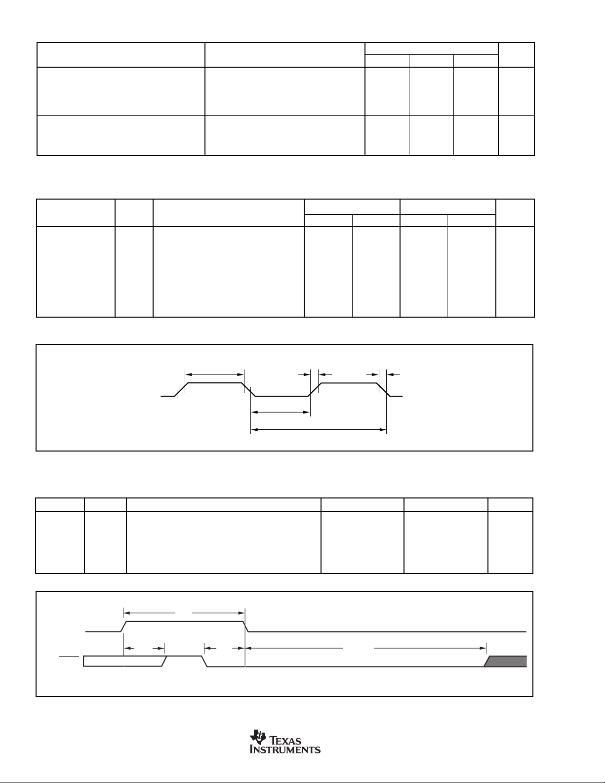
2.7V to 3.6V 4.75V to 5.25V
SYMBOL FIGURE PARAMETER MIN MAX MIN MAX UNITS
External Clock Mode
(1)
f
OSC
(1)
1/t
OSC
(1)
f
OSC
t
HIGH
t
LOW
t
R
t
F
NOTES: (1) t
CLK
= 1/f
A External Crystal Frequency (f
A External Clock Frequency (f
A External Ceramic Resonator Frequency (f
A HIGH Time
A LOW Time
A Rise Time
A Fall Time
= one oscillator clock period for clock divider = 1. (2) These values are characterized but not 100% production tested.
OSC
(2)
(2)
(2)
(2)
)120133MHz
OSC
)020033MHz
OSC
)1 12 1 12 MHz
OSC
15 10 ns
15 10 ns
55ns
55ns
t
HIGH
V
IH
V
IH
0.8V 0.8V
t
LOW
t
R
V
IH
V
IH
0.8V 0.8V
t
OSC
t
F
FIGURE A. External Clock Drive CLK.
SERIAL FLASH PROGRAMMING TIMING
SYMBOL FIGURE PARAMETER MIN MAX UNIT
t
RW
t
RRD
t
RFD
t
RS
t
RH
RST
P1.0/PROG
B RST width 2 t
OSC
— ns
B RST rise to P1.0 internal pull high — 5 µs
B RST falling to CPU start — 18 ms
B Input signal to RST falling setup time t
OSC
— ns
B RST falling to P1.0 hold time 18 — ms
t
RW
t
RRD
t
RS
, t
t
RFD
RH
NOTE: P1.0 is internally pulled-up with ~11kΩ during RST high.
FIGURE B. Serial Flash Programming Power-On Timing.
6
www.ti.com
MSC1200
SBAS289E
Page 7
PIN CONFIGURATION
Top View TQFP
NC
XIN
XOUT
DGND
RST
NC
NC
CAP
AV
AGND
AGND
AINCOM
DGNDNCDVDDP3.7
48 47 46 45 44 43 42
1
2
3
4
5
6
7
8
9
DD
10
11
12
13 14 15 16 17 18 19 20 21 22 233724
IDAC
REFIN–
P3.6/SCK/SCL/CLKS
P3.5/T1
MSC1200
NC
AIN7
AIN6
P3.4/T0
P3.3/INT1
P3.2/INT0
41 40 39 38
AIN5
AIN4
AIN3
P3.1/TxD0
P3.0/RxD0
AIN2
AIN1
P1.7/INT5
36
35
34
33
32
31
30
29
28
27
26
25
AIN0
DV
DD
DV
DD
DGND
DGND
P1.6/INT4
P1.5/INT3
P1.4/INT2/SS
P1.3/DIN
P1.2/DOUT
P1.1
P1.0/PROG
NC
REFOUT/REFIN+
MSC1200
SBAS289E
www.ti.com
7
Page 8
PIN DESCRIPTIONS
PIN # NAME DESCRIPTION
1,6,7,16,25,47 NC No Connection
2 XIN The crystal oscillator pin XIN supports parallel resonant AT cut fundamental frequency crystals and ceramic resonators.
3 X OUT The crystal oscillator pin XOUT supports parallel resonant AT cut fundamental frequency crystals and ceramic resonators.
4, 33, 34, 48 DGND Digital Ground
5 RST A HIGH on the reset input for two t
8 CAP Capacitor (220pF ceramic)
9AV
10, 11 AGND Analog Ground
12 AINCOM Analog Input (can be analog common for single-ended inputs or analog input for differential inputs)
13 IDAC IDAC Output
14 REFOUT/REF IN+ Internal Voltage Reference Output/Voltage Reference Positive Input
15 REF IN– Voltage Reference Negative Input (tie to AGND for internal voltage reference)
17 AIN7 Analog Input Channel 7
18 AIN6 Analog Input Channel 6
19 AIN5 Analog Input Channel 5
20 AIN4 Analog Input Channel 4
21 AIN3 Analog Input Channel 3
22 AIN2 Analog Input Channel 2
23 AIN1 Analog Input Channel 1
24 AIN0 Analog Input Channel 0
26-32, 37 P1.0-P1.7 Port 1 is a bidirectional I/O port (refer to P1DDRL, SFR AE
DD
XIN can also be an input if there is an external clock source instead of a crystal.
XOUT serves as the output of the crystal amplifier.
periods will reset the device.
OSC
Analog Power Supply
, and P1DDRH, SFR AFH, for port pin configuration control).
Port 1—Alternate Functions:
PORT ALTERNATE MODE
P1.0
P1.1 N/A
P1.2 DOUT Serial Data Out
P1.3 DIN Serial Data In
P1.4 INT2/
P1.5
P1.6 INT4 External Interrupt 4
P1.7
PROG
INT3
INT5
H
Serial Programming Mode
External Interrupt 2/Slave Select
SS
External Interrupt 3
External Interrupt 5
38-45 P3.0-P3.7 Port 3 is a bidirectional I/O port (refer to P3DDRL, SFR B3H, and P3DDRH, SFR B4H, for port pin configuration control).
35, 36, 46 DV
DD
Port 3—Alternate Functions:
Digital Power Supply
PORT ALTERNATE MODE
P3.0 RxD0 Serial Port 0 Input
P3.1 TxD0 Serial Port 0 Output
P3.2
P3.3
P3.4 T0 Timer 0 External Input
P3.5 T1 Timer 1 External Input
P3.6 SCK/SCL/CLKS SCK/SCL/Various Clocks (refer to PASEL, SFR F2
P3.7 N/A
INT0
INT1
External Interrupt 0
External Interrupt 1
)
H
8
www.ti.com
MSC1200
SBAS289E
Page 9
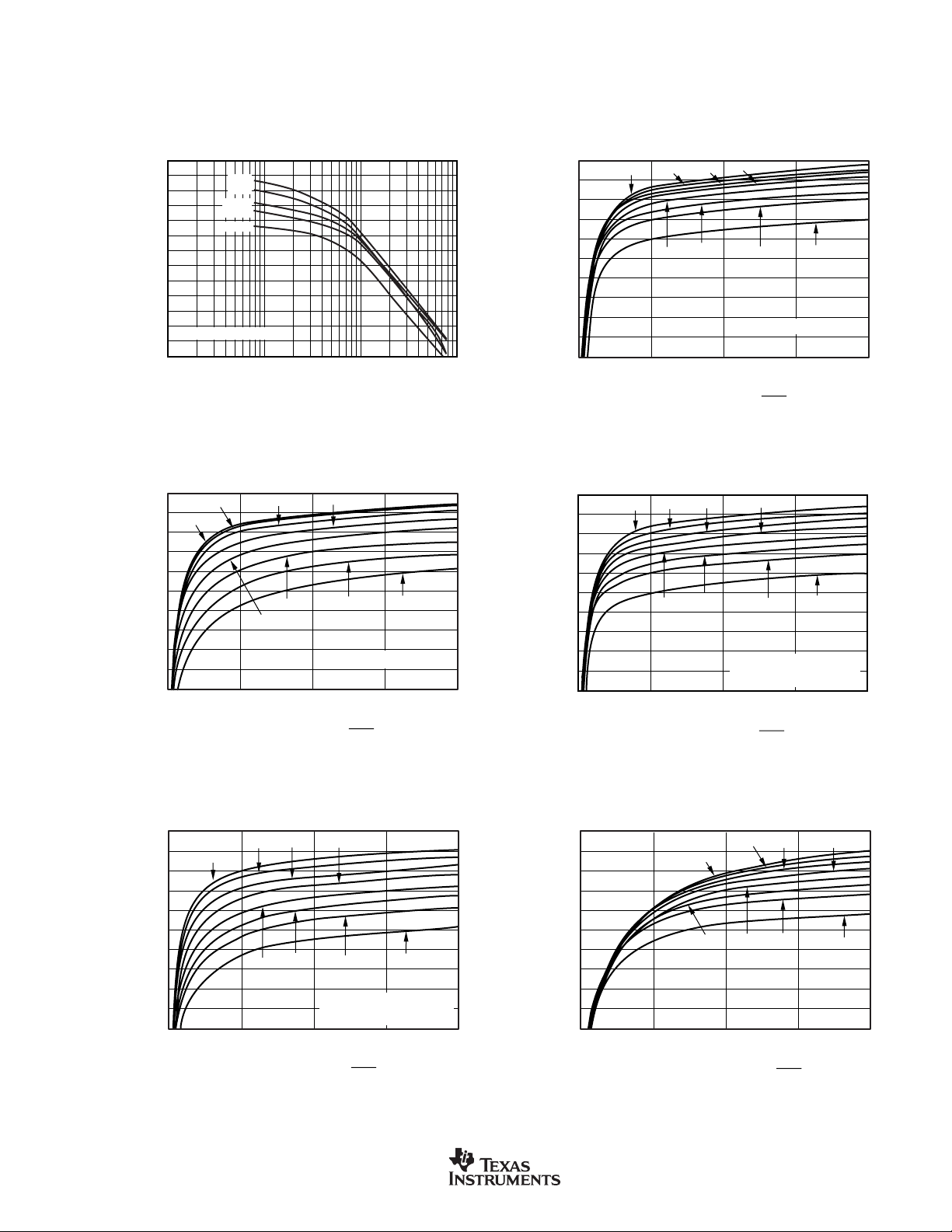
TYPICAL CHARACTERISTICS
22
21
20
19
18
17
16
15
14
13
12
EFFECTIVE NUMBER OF BITS
vs DECIMATION RATIO
Decimation Ratio =
f
MOD
f
DATA
0 500 1000 1500 2000
PGA4
ENOB (rms)
PGA1
PGA2
PGA16
PGA8
PGA32
PGA64 PGA128
Sinc3 Filter, Buffer OFF
22
21
20
19
18
17
16
15
14
13
12
EFFECTIVE NUMBER OF BITS
vs DECIMATION RATIO
0 500 1000 1500 2000
ENOB (rms)
PGA4
PGA8
PGA1
PGA2
PGA16
PGA32
PGA64
PGA128
Decimation Ratio =
f
MOD
f
DATA
AVDD = 3V, Sinc3 Filter,
V
REF
= 1.25V, Buffer OFF
22
21
20
19
18
17
16
15
14
13
12
EFFECTIVE NUMBER OF BITS
vs DECIMATION RATIO
0 500 1000 1500 2000
ENOB (rms)
PGA4
PGA8
PGA1
PGA2
PGA32
PGA128
PGA16 PGA64
Decimation Ratio =
f
MOD
f
DATA
Sinc2 Filter
AVDD = +5V, DVDD = +5V, f
EFFECTIVE NUMBER OF BITS vs DATA RATE
23
22
21
20
19
18
17
16
15
ENOB (rms)
14
13
12
Sinc3 Filter, Buffer OFF
11
10
1 10 100 1000
22
21
PGA2
PGA1
20
19
18
17
16
ENOB (rms)
15
14
13
12
0 500 1000 1500 2000
= 8MHz, PGA = 1, f
OSC
PGA1
PGA8
PGA32
PGA64
PGA128
Data Rate (SPS)
EFFECTIVE NUMBER OF BITS
vs DECIMATION RATIO
PGA32
PGA8
PGA64
PGA4
PGA16
Sinc3 Filter, Buffer ON
Decimation Ratio =
f
= 15.625kHz, Bipolar, Buffer ON, and V
MOD
PGA128
f
MOD
DATA
≡ (REF IN+) – (REF IN–) = +2.5V, unless otherwise specified.
REF
EFFECTIVE NUMBER OF BITS
vs DECIMATION RATIO
22
21
PGA2
PGA1
20
19
18
17
16
ENOB (rms)
15
14
13
12
0 500 1000 1500 2000
MSC1200
SBAS289E
PGA16
Decimation Ratio =
PGA4
PGA32
PGA8
PGA64
AVDD = 3V, Sinc3 Filter,
V
REF
PGA128
= 1.25V, Buffer ON
f
MOD
f
DATA
www.ti.com
9
Page 10
TYPICAL CHARACTERISTICS (Cont.)
AVDD = +5V, DVDD = +5V, f
= 8MHz, PGA = 1, f
OSC
= 15.625kHz, Bipolar, Buffer ON, and V
MOD
≡ (REF IN+) – (REF IN–) = +2.5V, unless otherwise specified.
REF
EFFECTIVE NUMBER OF BITS vs DECIMATION RATIO
FAST SETTLING FILTER
22
21
20
19
18
17
16
ENOB (rms)
15
14
13
Fast Settling Filter
12
0 500 1000 1500 2000
Decimation Ratio =
EFFECTIVE NUMBER OF BITS vs f
WITH FIXED DECIMATION
25
DEC = 2020
DEC = 500
1500
f
MOD
f
DATA
(set with ACLK)
MOD
20
DEC = 50
DEC = 20
DEC = 10
15
10
ENOB (rms)
5
DEC = 255
0
10 100 1k 10k 100k
Data Rate (SPS)
EFFECTIVE NUMBER OF BITS vs f
(set with ACLK)
MOD
25
f
= 203kHz
f
MOD
MOD
= 62.5kHz
f
MOD
= 110kHz
20
15
10
ENOB (rms)
5
f
MOD
= 15.6kHz
f
= 31.25kHz
MOD
0
1 10 100 1k 10k 100k
Data Rate (SPS)
NOISE vs INPUT SIGNAL
0.8
0.7
0.6
0.5
0.4
0.3
0.2
Noise (rms, ppm of FS)
0.1
0
–2.5 –1.5 0.5–0.5 1.5 2.5
(V)
V
IN
10
−2
INL (ppm of FS)
−4
−6
−8
−10
10
INTEGRAL NONLINEARITY vs INPUT SIGNAL
V
= 2.5V
8
REF
6
4
2
–40°C
+85°C
0
+25°C
−2.5 −2.0 −1.0 −0.5−1.5 0 0.5 1.0 1.5 2.0 2.5
(V)
V
IN
www.ti.com
15
10
5
0
−5
INL (ppm of FS)
−10
−15
= −V
V
IN
REF
INTEGRAL NONLINEARITY vs INPUT SIGNAL
V
= AVDD = 5V
REF
Buffer OFF
0V
V
(V)
IN
MSC1200
SBAS289E
IN
= +V
REF
Page 11
TYPICAL CHARACTERISTICS (Cont.)
10
8
6
4
2
0
–2
–4
–6
–8
–10
–12
OFFSET DAC: OFFSET vs TEMPERATURE
Offset (ppm of FSR)
Temperature (°C)
–40 +25 +85
AVDD = +5V, DVDD = +5V, f
= 8MHz, PGA = 1, f
OSC
= 15.625kHz, Bipolar, Buffer ON, and V
MOD
≡ (REF IN+) – (REF IN–) = +2.5V, unless otherwise specified.
REF
30
ADC INTEGRAL NONLINEARITY vs V
25
Buffer OFF
20
15
10
INL (ppm of FS)
AVDD = 3V
AVDD = 5V
5
0
0 0.5 1.0 1.5 2.0 2.5 3.0 3.5 4.0 4.5 5.0 5.5
V
(V)
REF
ANALOG SUPPLY CURRENT
1.3
1.3
1.2
PGA = 128, ADC = ON
1.2
V
= ON, DBOR = ON
REF
ALVD = ON, IDAC = ON
1.1
1.1
1.0
Analog Supply Current (mA)
1.0
0.9
2.5 3.0 3.5 4.0 4.5 5.0 5.5
Analog Supply Voltage (V)
REF
VIN = V
+85°C
+25°C
–40°C
REF
50
AVDD = 5V
45
V
= 2.5V
REF
40
35
30
25
20
INL (ppm of FS)
15
10
5
0
142168 1286432
INL ERROR vs PGA
PGA Setting
ADC CURRENT vs PGA
0.8
0.7
AVDD = 5V, Buffer = ON
0.6
0.5
(µA)
0.4
ADC
I
0.3
AVDD = 3V, Buffer = ON
AVDD = 5V, Buffer = OFF
AVDD = 3V, Buffer = OFF
0.2
0.1
1824 3216 12864
PGA Setting
4500
4000
3500
3000
2500
2000
1500
Number of Occurrences
1000
500
0
–2
HISTOGRAM OF OUTPUT DATA
–1.5 –1 –0.5 0 0.5 1 1.5 2
MSC1200
SBAS289E
ppm of FS
www.ti.com
11
Page 12

TYPICAL CHARACTERISTICS (Cont.)
AVDD = +5V, DVDD = +5V, f
= 8MHz, PGA = 1, f
OSC
= 15.625kHz, Bipolar, Buffer ON, and V
MOD
≡ (REF IN+) – (REF IN–) = +2.5V, unless otherwise specified.
REF
1.00006
1.00004
1.00002
1
0.99998
Normalized Gain
0.99996
0.99994
–40 +25 +85
100
Digital Supply Current (mA)
DIGITAL SUPPLY CURRENT vs CLOCK DIVIDER
10
1
OFFSET DAC: GAIN vs TEMPERATURE
Temperature (°C)
Divider Values
1
2
4
8
16
32
1024
100
10
Digital Supply Current (mA)
0.1
10
Digital Supply Current (mA)
DIGITAL SUPPLY CURRENT vs FREQUENCY
1
DVDD = 5V
1 10 100
Clock Frequency (MHz)
DIGITAL SUPPLY CURRENT vs SUPPLY VOLTAGE
8
+25°C
6
4
2
+85°C
–40°C
0.1
1 10 100
Clock Frequency (MHz)
NORMALIZED GAIN vs PGA
101
100
99
98
97
Normalized Gain (%)
96
95
142168 1286432
PGA Setting
Buffer ON
0
2.7 3.1 3.5 3.9 4.3 4.7 5.1
Supply Voltage (V)
5.0
4.5
4.0
3.5
3.0
2.5
2.0
1.5
Output Voltage (V)
1.0
0.5
0
02010 4030 706050
CMOS DIGITAL OUTPUT
3V
Low
Output
3V
Output Current (mA)
5V
Low
Output
5V
12
www.ti.com
MSC1200
SBAS289E
Page 13

TYPICAL CHARACTERISTICS (Cont.)
IO HF MODE vs FREQUENCY
Temperature (°C)
IO Frequency (MHz)
−40 25 85
28
27
26
25
24
23
4.75V
5.25V
AVDD = DV
DD
AVDD = +5V, DVDD = +5V, f
14
AVDD = DV
13
12
IO Frequency (MHz)
11
10
−40 25 85
IO LF MODE vs TEMPERATURE
DD
= 8MHz, PGA = 1, f
OSC
4.75V
Temperature (°C)
= 15.625kHz, Bipolar, Buffer ON, and V
MOD
5.25V
3.3V
2.7V
≡ (REF IN+) – (REF IN–) = +2.5V, unless otherwise specified.
REF
MSC1200
SBAS289E
www.ti.com
13
Page 14
DESCRIPTION
The MSC1200Yx is a completely integrated family of mixedsignal devices incorporating a high-resolution delta-sigma
ADC, 8-bit IDAC, 8-channel multiplexer, burnout detect current sources, selectable buffered input, offset DAC, programmable gain amplifier (PGA), temperature sensor, voltage
reference, 8-bit microcontroller, Flash Program Memory, Flash
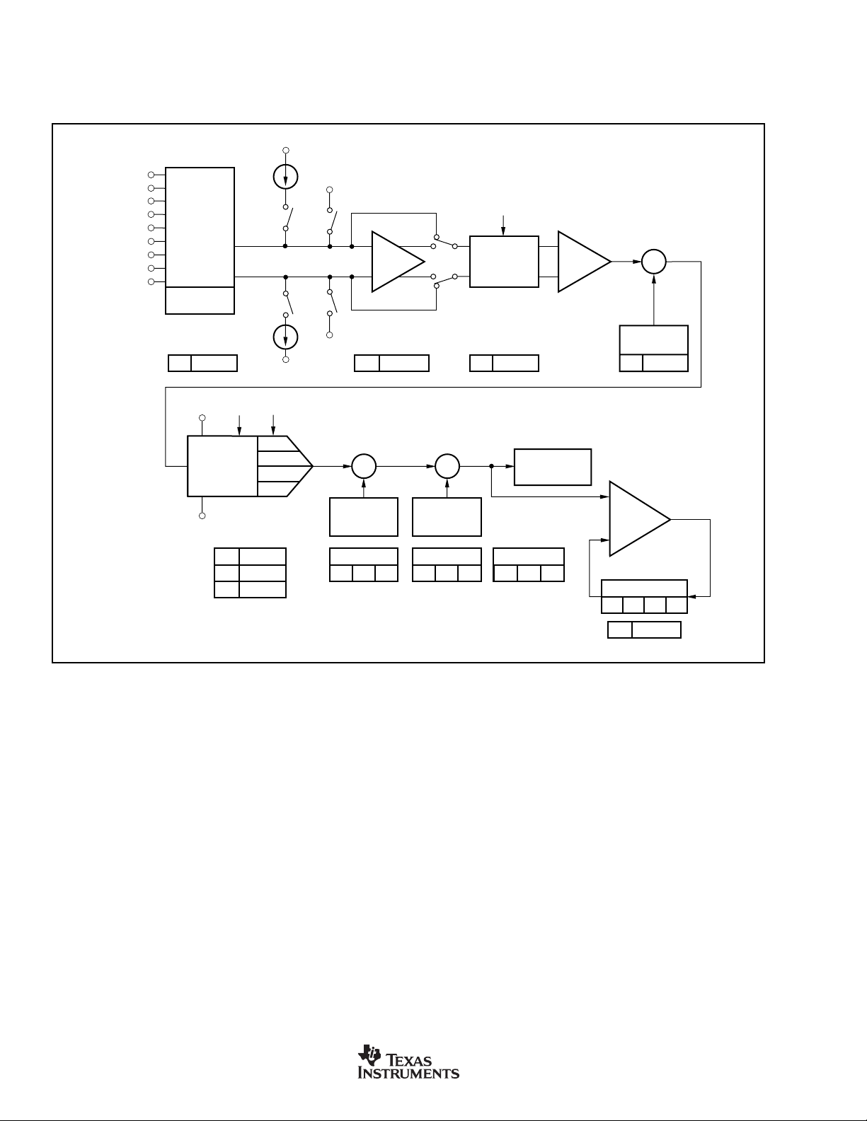
Data Memory, and Data SRAM, as shown in Figure 1.
On-chip peripherals include an additional 32-bit accumulator,
basic SPI, basic I
ports, watchdog timer, low-voltage detect, on-chip power-on
reset, brownout reset, timer/counters, system clock divider,
PLL, on-chip oscillator, and external interrupts.
The device accepts low-level differential or single-ended
signals directly from a transducer. The ADC provides 24 bits
of resolution and 24 bits of no-missing-code performance
using a Sinc
ADC also has a selectable filter that allows for high-resolution single-cycle conversion.
The microcontroller core is 8051 instruction set compatible. The
microcontroller core is an optimized 8051 core that executes up
to three times faster than the standard 8051 core, given the
same clock source. This makes it possible to run the device at
a lower external clock frequency and achieve the same performance at lower power than the standard 8051 core.
2
C, USART, multiple digital input/output
3
filter with a programmable sample rate. The
The MSC1200Yx allows the user to uniquely configure the
Flash memory map to meet the needs of their application.
The Flash is programmable down to 2.7V using serial programming. Flash endurance is typically 1M Erase/Write cycles.
The part has separate analog and digital supplies, which can
be independently powered from 2.7V to +5.25V. At +3V
operation, the power dissipation for the part is typically less
than 4mW. The MSC1200Yx is packaged in a TQFP-48
package.
The MSC1200Yx is designed for high-resolution measurement
applications in smart transmitters, industrial process control,
weigh scales, chromatography, and portable instrumentation.
ENHANCED 8051 CORE
All instructions in the MSC1200 family perform exactly the same
functions as they would in a standard 8051. The effect on bits,
flags, and registers is the same. However, the timing is different.
The MSC1200 family utilizes an efficient 8051 core which results
in an improved instruction execution speed of between 1.5 and
3 times faster than the original core for the same external clock
speed (4 clock cycles per instruction versus 12 clock cycles per
instruction, as shown in Figure 2). This translates into an effective
throughput improvement of more than 2.5 times, using the same
code and same external clock speed. Therefore, a device
frequency of 33MHz for the MSC1200Yx actually performs at an
equivalent execution speed of 82.5MHz compared to the
AIN0
AIN1
AIN2
AIN3
AIN4
AIN5
AIN6
AIN7
AINCOM
IDAC
FIGURE 1. Block Diagram.
instr_cycle
AGND REFOUT/REFIN+ REFIN– DVDDDGND
AV
DD
AV
DD
Burnout
Detect
Temperature
Sensor
MUX
AGND
NOTE (1) REF IN− must be tied to AGND when using internal V
CLK
BUFFER PGA
Burnout
Detect
8-Bit IDAC
n + 1 n + 2
V
REF
8-Bit
Offset DAC
REF
Modulator
4K or 8K
FLASH
128 Bytes
SRAM
.
POR
(1)
ALVD
DBOR
Digital
System
Clock
Divider
Filter
ACC
8051
SFR
Timers/
Counters
WDT
PORT1
PORT3
On-Chip
Oscillator
PLL
XIN XOUT
RST
CAP
Alternate
Functions
DIN
DOUT
SS
EXT (4)
PROG
USART
EXT (2)
T0
T1
SCK/SCL/CLKS
220pF Ceramic
cpu_cycle
FIGURE 2. Instruction Cycle Timing.
14
C1 C2 C3 C4 C1 C2 C3 C4 C1
www.ti.com
MSC1200
SBAS289E
Page 15
standard 8051 core. This allows the user to run the device at
slower clock speeds, which reduces system noise and power
consumption, but provides greater throughput. This performance
difference can be seen in Figure 3. The timing of software loops
will be faster with the MSC1200. However, the timer/counter
operation of the MSC1200 may be maintained at 12 clocks per
increment or optionally run at 4 clocks per increment.
Single-Byte, Single-Cycle
Instruction
ALE
PSEN
Internal
AD0-AD7
Internal
A8-A15
4 Cycles
CLK
12 Cycles
ALE
PSEN
AD0-AD7
PORT 2
Standard 8051 Timing MSC1200 Timing
Single-Byte, Single-Cycle
Instruction
FIGURE 3. Comparison of MSC1200 Timing to Standard
8051 Timing.
The MSC1200 also provides dual data pointers (DPTRs).
Furthermore, improvements were made to peripheral fea-
tures that off-load processing from the core and the user, to
further improve efficiency. For instance, a 32-bit accumulator
was added to significantly reduce the processing overhead
for the multiple byte data from the ADC or other sources. This
allows for 24-bit addition and shifting to be accomplished in
a few instruction cycles, compared to hundreds of instruction
cycles through software implementation.
Family Device Compatibility
The hardware functionality and pin configuration across the
MSC1200 family is fully compatible. To the user, the only
difference between family members is the memory configuration.
This makes migration between family members simple. Code
written for the MSC1200Y2 can be executed directly on an
MSC1200Y3. This gives the user the ability to add or subtract
software functions and to freely migrate between family members. Thus, the MSC1200 can become a standard device used
across several application platforms.
Family Development Tools
The MSC1200 is fully compatible with the standard 8051
instruction set. This means that the user can develop software for the MSC1200 with existing 8051 development tools.
Additionally, a complete, integrated development environment is provided with each demo board, and third-party
developers also provide support.
Power Down Modes
The MSC1200 can power several of the peripherals and put
the CPU into IDLE. This is accomplished by shutting off the
clocks to those sections, as shown in Figure 4.
t
SYS
SYSCLK
t
CLK
USEC
MSECH
ADC Power Down
PDCON.3
IDLE
C7
9A
Flash Write
Timing
Flash Erase
Timing
SECINT
WDTCON
SCL/SCK
(30µs to 40µs)
(5ms to 11ms)
milliseconds
interrupt
FA
ADC Output Rate
F9
FF
seconds
interrupt
watchdog
FD
ACLK
FB
MSECL
FC
F6
Timers 0/1
CPU Clock
PDCON.0
ms
PDCON.1
HMSEC
divide
by 64
Modulator Clock
SPICON/
I2CCON
µs
FE
ADCON3 ADCON2
FTCON
[3:0]
FTCON
[7:4]
100ms
PDCON.2
DF DE
Decimation Ratio
USART
EF
EF
MSINT
FIGURE 4. MSC1200 Timing Chain and Clock Control.
MSC1200
SBAS289E
www.ti.com
15
Page 16
OVERVIEW
The MSC1200 ADC structure is shown in Figure 5. The figure lists the components that make up the ADC, along with the
corresponding special function register (SFR) associated with each component.
AV
DD
AIN0
AIN1
AIN2
AIN3
AIN4
AIN5
AIN6
AIN7
AINCOM
Input
Multiplexer
Temperature
Sensor
ADMUXD7
H
REFIN+ f
V
IN
∆Σ ADC
Modulator
REFIN−
Burnout
MOD
H
H
H
Burnout
Detect
Detect
ADCON1DD
ADCON2DE
ADCON3DF
In+
In−
AGND
f
DATA
FAST
SINC2
SINC3
AUTO
REFIN+
Buffer PGA
REFIN−
ADCON0DC
H
Σ X
Offset
Calibration
Register
OCR GCR ADRES
D3
HD2HD1H
Gain
Calibration
Register
D6HD5HD4HDBHDAHD9
f
SAMP
Sample
and Hold
ACLKF6
H
ADC
Result Register
H
Σ
Offset
DAC
ODACE6
H
Summation
Block
Σ
SUMR
E5HE4HE3HE2
E1
SSCON
H
H
FIGURE 5. MSC1200 ADC Structure.
16
www.ti.com
MSC1200
SBAS289E
Page 17
INPUT MULTIPLEXER
R
SWITCH
(3kΩ typical)
Sampling Frequency = f
SAMP
High Impedance
> 1GΩ
C
S
AGND
A
IN
PGA f
SAMP
1, 2, 4 f
MOD
82 × f
MOD
16 4 × f
MOD
32 8 × f
MOD
64, 128 16 × f
MOD
PGA C
S
1 9pF
2 18pF
4 to 128 36pF
The input multiplexer provides for any combination of differential
inputs to be selected as the input channel, as shown in Figure 6.
If AIN0 is selected as the positive differential input channel, any
other channel can be selected as the negative differential input
channel. With this method, it is possible to have up to eight fully
differential input channels. It is also possible to switch the polarity
of the differential input pair to negate any offset voltages.
AIN0
AIN1
AIN2
AV
DD
Burnout Detect (2µA)
BURNOUT DETECT
When the Burnout Detect (BOD) bit is set in the ADC control
configuration register (ADCON0 DC
), two current sources are
H
enabled. The current source on the positive input channel sources
approximately 2µA of current. The current source on the negative
input channel sinks approximately 2µA. This allows for the
detection of an open circuit (full-scale reading) or short circuit
(small differential reading) on the selected input differential pair.
Enabling the buffer is recommended when BOD is enabled.
INPUT BUFFER
The analog input impedance is always high, regardless of
PGA setting (when the buffer is enabled). With the buffer
enabled, the input voltage range is reduced and the analog
power-supply current is higher. If the limitation of input
voltage range is acceptable, then the buffer is always preferred.
The input impedance of the MSC1200 without the buffer
is 7MΩ/PGA. The buffer is controlled by the state of the BUF
bit in the ADC control register (ADCON0 DC
).
H
AIN3
In+
AIN4
In–
AIN5
AIN6
AGND
AIN7
AINCOM
Buffer
Burnout Detect (2µA)
Temperature Sensor
AV
DD
80 • I
AV
DD
I
FIGURE 6. Input Multiplexer Configuration.
In addition, current sources are supplied that will source or
sink current to detect open or short circuits on the pins.
ANALOG INPUT
When the buffer is not selected, the input impedance of the
analog input changes with ACLK clock frequency (ACLK
F6
) and gain (PGA). The relationship is:
H
A pedance
Im ( )Ω=
IN
where ACLK frequency (f
f
and f
MOD
=
ACLK
64
.
MHz
17
ACLKFrequencyMPGA
) =
ACLK
Figure 7 shows the basic input structure of the MSC1200.
f
CLK
ACLK
+1
Ω
•
TEMPERATURE SENSOR
On-chip diodes provide temperature sensing capability. When
the configuration register for the input MUX is set to all 1s,
the diodes are connected to the input of the ADC. All other
channels are open.
MSC1200
SBAS289E
FIGURE 7. Analog Input Structure (without buffer).
www.ti.com
17
Page 18

PGA
The PGA can be set to gains of 1, 2, 4, 8, 16, 32, 64, or 128.
Using the PGA can actually improve the effective resolution
of the ADC. For instance, with a PGA of 1 on a ±2.5V fullscale range, the ADC can resolve to 1.5µV. With a PGA of
128 on a ±19mV full-scale range, the ADC can resolve to
75nV. With a PGA of 1 on a ±2.5V full-scale range, it would
require a 26-bit ADC to resolve 75nV, as shown in Table I.
PGA RANGE AT 10Hz RESOLUTION
FULL-SCALE ENOB MEASUREMENT
SETTING (V) (BITS) (nV)
1 ±2.5 21.7 1468
2 ±1.25 21.5 843
4 ±0.625 21.4 452
8 ±0.313 21.2 259
16 ±0.156 20.8 171
32 ±0.0781 20.4 113
64 ±0.039 20 74.5
128 ±0.019 19 74.5
RMS
TABLE I. ENOB Versus PGA.
OFFSET DAC
The analog output from the PGA can be offset by up to half
the full-scale input range of the PGA by using the ODAC
register (SFR E6
bit value; the MSB is the sign and the seven LSBs provide
the magnitude of the offset. Since the ODAC introduces an
analog (instead of digital) offset to the PGA, using the ODAC
does not reduce the range of the ADC.
). The ODAC (Offset DAC) register is an 8-
H
requires a positive full-scale differential input signal. It then
computes a gain value to nullify gain errors in the system.
Each of these calibrations will take seven t
periods to
DATA
complete.
Calibration should be performed after power on, a change in
temperature, power supply, voltage reference, decimation
ratio, buffer, or a change of the PGA. Calibration will remove
the effects of the Offset DAC; therefore, changes to the
Offset DAC register should be done after calibration.
At the completion of calibration, the ADC Interrupt bit goes
high, which indicates the calibration is finished and valid data
is available.
DIGITAL FILTER
The Digital Filter can use either the Fast Settling, Sinc2, or
3
Sinc
filter, as shown in Figure 8. In addition, the Auto mode
changes the Sinc filter after the input channel or PGA is
changed. When switching to a new channel, it will use the
Fast Settling filter, for the next two conversions the first of
which should be discarded. It will then use the Sinc
by the Sinc
3
filter to improve noise performance. This combines the low-noise advantage of the Sinc
quick response of the Fast Settling Time filter. The frequency
response of each filter is shown in Figure 9.
Adjustable Digital Filter
3
Sinc
2
followed
3
filter with the
MODULATOR
The modulator is a single-loop 2nd-order system. The modulator runs at a clock speed (f
using the value in the Analog Clock register (ACLK, F6
) that is derived from the CLK
MOD
H
The data output rate is:
f
MOD
DecimationRatio
f
=
where f
Data Rate = f
=
MOD
ACLK
()+•
=
DATA
f
CLK ACLK
164 64
CALIBRATION
The offset and gain errors in the MSC1200, or the complete
system, can be reduced with calibration. Calibration is controlled through the ADCON1 register (SFR DD
CAL2:CAL0. Each calibration process takes seven t
periods (data conversion time) to complete. Therefore, it
takes 14 t
periods to complete both an offset and gain
DATA
calibration.
For system calibration, the appropriate signal must be
applied to the inputs. The system offset calibration requires a
zero-differential input signal. It then computes an offset value
that will nullify offset in the system. The system gain calibration
), bits
H
DATA
Modulator
).
FILTER SETTLING TIME
FILTER (Conversion Cycles)
3
Sinc
2
Sinc
Fast 1
NOTE: (1) With Synchronized Channel Changes.
AUTO MODE FILTER SELECTION
1234+
Discard Fast Sinc
FIGURE 8. Filter Step Responses.
2
Sinc
Fast Settling
SETTLING TIME
CONVERSION CYCLE
Data Out
(1)
3
(1)
2
(1)
2
Sinc
3
18
www.ti.com
MSC1200
SBAS289E
Page 19

0
PROG
–20
–40
–60
Gain (dB)
–80
–100
SINC3 FILTER RESPONSE
(–3dB = 0.262 • f
DATA
If the internal V
is not used, then V
REF
should be disabled
REF
in ADCON0.
)
If the external voltage reference is selected it can be used as
either a single-ended input of differential input, for ratiometric
measures. When using an external reference, it is important
to note that the input current will increase for V
with higher
REF
PGA settings and with a higher modulator frequency. The
external voltage reference can be used over the input range
specified in the electrical characteristics section.
–120
012345
0
–20
–40
–60
Gain (dB)
–80
–100
–120
012345
0
–20
–40
–60
Gain (dB)
–80
–100
–120
012345
SINC2 FILTER RESPONSE
FAST SETTLING FILTER RESPONSE
NOTE: f
DATA
f
DATA
(–3dB = 0.318 • f
f
DATA
(–3dB = 0.469 • f
f
DATA
= Data Output Rate = 1/t
DATA
DATA
DATA
)
)
FIGURE 9. Filter Frequency Responses.
VOLTAGE REFERENCE
The MSC1200 can use either an internal or external voltage
reference. The voltage reference selection is controlled via
ADC Control Register 0 (ADCON0, SFR DC
power-up configuration for the voltage reference is 2.5V
internal.
The internal voltage reference can be selected as either 1.25V
or 2.5V. The analog power supply (AV
DD
specified range for the selected internal voltage reference.
The valid ranges are: V
5.25V) and V
internal V
= 1.25 internal (AVDD = 2.7V to 5.25V). If the
REF
is selected then AGND must be connected to
REF
= 2.5 internal (AVDD = 4.1V to
REF
REFIN–. The REFOUT/REFIN+ pin should also have a 0.1µF
capacitor connected to AGND as close as possible to the pin.
). The default
H
) must be within the
IDAC
The 8-bit IDAC in the MSC1200 can be used to provide a
current source that can be used for ratiometric measurements. The IDAC operates from its own voltage reference
and is not dependent on the ADC voltage reference. The fullscale output current of the IDAC is approximately 1mA. The
equation for the IDAC output current is:
IDACOUT = IDAC • 3.6µA
RESET
Taking the RST pin HIGH will stop the operation of the
device, and taking the RST pin LOW will initiate a reset. The
device can also be reset by the power on reset circuitry,
digital brownout Reset, or software reset. The timing of the
reset operation is shown in the Electrical Characteristics
section.
If the P1.0/PROG
pin is unconnected or tied HIGH, the
device will enter User Application mode on reset. If P1.0/
is tied LOW during reset, the device will enter Serial
Programming mode.
POWER ON RESET
The on-chip Power On Reset (POR) circuitry releases the
device from reset at approximately DVDD = 2.0V. The POR
accommodates power-supply ramp rates as slow as
1V/10ms. To ensure proper operation, the power supply
should ramp monotonically. Note that, as the device is
released from reset and program execution begins, the
device current consumption may increase, which may result
in a power-supply voltage drop. If the power supply ramps at
a slower rate, is not monotonic, or a brownout condition
occurs (where the supply does not drop below the 2.0V
threshold), then improper device operation may occur. The
on-chip Brownout Reset (BOR) may provide benefit in these
conditions. A POR circuit is shown in Figure 10.
DV
DD
0.1µF
10kΩ
1MΩ
FIGURE 10. Typical Reset Circuit.
5
MSC1200
RST
MSC1200
SBAS289E
www.ti.com
19
Page 20

DIGITAL BROWNOUT RESET
The Digital Brownout Reset (DBOR) is enabled through
Hardware Configuration Register 1 (HCR1). If the conditions
for proper POR are not met or the device encounters a
brownout condition which does not generate a POR, DBOR
can be used to ensure proper device operation. The DBOR
will hold the state of the device when the power supply drops
below the threshold level programmed in HCR1 and then
generate a reset when the supply rises above the threshold
level. Note that, as the device is released from reset and
program execution begins, the device current consumption
may increase, which can result in a power-supply voltage
drop, which may initiate another brownout condition. Additionally, the DBOR comparison is done against an analog
reference; therefore, AV
must be within its valid operating
DD
range for DBOR to function.
The DBOR level should be chosen to match closely with the
application. That is, with a high external clock frequency, the
BOR level should match the minimum operating voltage
range for the device, or improper operation may still occur.
ANALOG LOW VOLTAGE DETECT
The MSC1200 contains an analog low-voltage detect. When
the analog supply drops below the value programmed in
LVDCON (SFR E7
), an interrupt is generated.
H
POWER-UP—SUPPLY VOLTAGE RAMP RATE
The built-in (on-chip) power-on reset circuitry was designed
to accommodate analog or digital supply ramp rates as slow
as 1V/10ms. To ensure proper operation, the power supply
should ramp monotonically at the specified rate. If DBOR is
enabled, the ramp rate can be slower.
CLOCKS
The MSC1200 can operate in three separate clock modes:
internal oscillator mode (IOM), external clock mode (ECM),
and PLL mode. A block diagram is shown in Figure 11. The
clock mode for the MSC1200 is selected via the CLKSEL bits
in HCR2. IOM is the default mode for the device.
Serial Flash Programming mode uses IO LF mode (the
HCR2 and CLKSEL bits have no effect). Table II shows the
active clock mode for the various startup conditions.
Internal Oscillator
In IOM, the CPU executes either in LF mode (if HCR2,
CLKSEL = 111) or HF mode (if HCR2, CLKSEL = 110).
External Clock
In ECM (HCR2, CLKSEL = 011), the CPU can execute from
an external crystal, external ceramic resonator, external
STOP
Int Osc
PLLDIV
100kΩ
CAP
220pF
Ceramic
VCO
(1)
PLL DAC
XIN
XOUT
Phase
Detector
NOTE: (1) The trace length connecting the CAP pin to the 220pF ceramic capacitor should be as short as possible.
Charge
Pump
LF/HF Mode
FIGURE 11. Clock Block Diagram.
SELECTED CLOCK MODE (HCR2, CLKCON2:0) STARTUP CONDITION
External Clock Mode (ECM)
Internal Oscillator Mode (IOM)
IO LF Mode N/A IO LF Mode
IO HF Mode N/A IO HF Mode
(2)
PLL
PLL LF Mode Active 32.768kHz Clock at XIN PLL LF Mode
PLL HF Mode Active 32.768kHz Clock at XIN PLL HF Mode
NOTES: (1) Clock detection is only done at startup; refer to Electrical Characteristics parameter t
(2) PLL operation requires that both AVDD and DVDD are within their specified operating range.
Active Clock Present at XIN External Clock Mode
No Clock Present at XIN IO LF Mode
No Clock Present at XIN Nominal: 50% of IO LF Mode Rate
No Clock Present at XIN Nominal: 50% of IO HF Mode Rate
(1)
ACTIVE CLOCK MODE (f
in Figure B.
RFD
TABLE II. Active Clock Modes.
t
PLL/tIOM
t
OSC
t
SYS
SYSDIV
)
SYS
t
CLK
20
www.ti.com
MSC1200
SBAS289E
Page 21

XINExternal Clock
clock, or external oscillator. If an external clock is detected at
SPI /I2C
Data Write
SPICON
I2CCON
I2C
Stretch
Control
Counter
Start/Stop
Detect
SPI /I2C
Data Read
Pad Control
DOUT
P1.2
P1.4
P3.6
P1.3
Logic
DOUT
TX_CLK
RX_CLK
SS
SCK/SCL
CNT_CLK
CNT INT
I2C INT
DIN
CLKS
(refer to PASEL, SFR F2
H
)
SS
SCK
DIN
startup, then the CPU will begin execution in ECM after
startup. If an external clock is not detected at startup, then
the device will revert to the mode shown in Table II.
XIN
C
1
PLL
In Phase Lock Loop (PLL) mode (HCR2, CLKSEL = 101 or
HCR2, CLKSEL = 100), the CPU can execute from an
external 32.768 kHz crystal. This mode enables the use of a
phase-lock loop (PLL) circuit that synthesizes the selected
clock frequencies (PLL LF mode or PLL HF mode). If an
external clock is detected at startup, then the CPU will begin
execution in PLL mode after startup. If an external clock is
not detected at startup, then the device will revert to the
mode shown in Table II. The status of the PLL can be
determined by first writing the PLLLOCK bit (enable) and
then reading the PLLLOCK status bit in the PLLH SFR.
The frequency of the PLL is preloaded with default trimmed
values. However, the PLL frequency can be fine-tuned by
writing to the PLLDIV1 and PLLDIV0 SFRs. The equation for
the PLL frequency is:
PLL Frequency = ((PLLDIV9:PLLDIV0) + 1) • f
where f
= 32.768kHz.
OSC
OSC
The default value for PLL LF mode is automatically loaded
into the PLLDIV SFR. For PLL HF mode, the user must load
PLLDIV with the appropriate value (0383
).
H
For different connections to external clocks, see Figures 12,
13, and 14.
SPI
The MSC1200 implements a basic SPI interface which includes the hardware for simple serial data transfers. Figure 15
shows a block digram of the SPI. The peripheral supports
master and slave mode, full duplex data transfers, both clock
polarities, both clock phases, bit order, and slave select.
XOUT
C
2
NOTE: Refer to the crystal manufacturer's specification
for C
and C2 values.
1
FIGURE 12. External Crystal Connection.
FIGURE 13. External Clock Connection.
C
1
C
2
32.768kHz
NOTE: Typical configuration is shown.
R
S
FIGURE 14. PLL Connection.
XIN
XOUT
FIGURE 15. SPI/I2C Block Diagram.
MSC1200
SBAS289E
www.ti.com
21
Page 22

The timing diagram for supported SPI data transfers is
shown in Figure 16.
The I/O pins needed for data transfer are Data In (DIN), Data
Out (DOUT) and serial clock (SCK). The slave select (
SS
pin can also be used to control the output of data on DOUT.
The DIN pin is used for shifting data in for both master and
slave modes.
The DOUT pin is used for shifting data out for both master
and slave modes.
The SCK pin is used to synchronize the transfer of data for
both master and slave modes. SCK is always generated by
the master. The generation of SCK in master mode can be
done in SW by simply toggling the port pin, or the generation
of SCK can be accomplished by configuring the output on the
SCK pin via PASEL (SFR F2
). A list of the most common
H
methods of generating SCK follows, but the complete list of
clock sources can be found by referring to the PASEL SFR.
• Toggle SCK by setting and clearing the port pin.
• Memory Write Pulse (WR) which is idle high. Whenever a
external memory write command (MOVX) is executed then a
pulse is seen on P3.6. This method can be used only if CPOL
is set to ‘1’.
• Memory Write Pulse toggle version: In this mode, SCK
toggles whenever an external write command (MOVX) is
executed.
• T0_Out signal can be used as a clock. A pulse is generated
on SCK whenever Timer 0 expires. The idle state of the
signal is low, so this can be used only if CPOL is cleared to
‘0’.
• T0_Out Toggle: SCK toggles whenever Timer 0 expires.
• T1_Out signal can be used as a clock. A pulse is generated
whenever Timer 1 expires. The idle state of the signal is low,
so this can be used only if CPOL is cleared to ‘0’.
• T1_Out Toggle: SCK toggles whenever Timer 1 expires.
The
SS
pin can be used to control the output of data on
DOUT when the MSC1200 is in slave mode. The
is enabled or disabled by the ESS bit of the SPICON SFR.
When enabled, the
)
SS
input of a slave device must be
externally asserted before a master device can exchange
data with the slave device.
SS
must be low before data
transactions and must stay low for the duration of the
transaction. When
SS
is high then data will not be shifted into
the shift register nor will the counter increment. When SPI is
enabled,
When
and when
SS
also controls the drive of the line DOUT (P1.2).
SS
is low in slave mode, the DOUT pin will be driven
SS
is high then DOUT will be high impedance.
The SPI generates an interrupt ECNT (AIE.2) to indicate that
the transfer/reception of the byte is complete. The interrupt
goes high whenever the counter value is equal to 8 (indicating that 8 SCKs have occurred). The interrupt is cleared on
reading or writing to the SPIDATA register. During the data
transfer, the actual counter value can be read from the
SPICON SFR.
Power Down
The SPI is powered down by the PDSPI bit in the power
control register (PDCON). This bit needs to be cleared to
enable the SPI function. When the SPI is powered down the
pins P1.2, P1.3, P1.4, and P3.6 revert to general-purpose
I/O pins.
Application Flow
Explained below are the steps of the typical application
usage flow of SPI in master and slave mode:
Master Mode Application Flow
1. Configure the port pins.
2. Configure the SPI.
SS
3. Assert
4. Write data to SPIDATA.
5. Generate 8 SCKs.
6. Read the received data from SPIDATA.
to enable slave communications (if applicable).
SS
function
SCK Cycle #
SCK (CPOL = 0)
SCK (CPOL = 1)
Sample Input
(CPHA = 0) Data Out
Sample Input
(CPHA = 1) Data Out
SS to Slave
1) SS Asserted
2) First SCK Edge
3) CNTIF Set (dependent on CPHA bit)
4) SS Negated
1
FIGURE 16. SPI Timing Diagram.
22
12345678
MSB654321LSB
MSB654321 LSB
2
Slave CPHA = 1 Transfer in Progress
Slave CPHA = 0 Transfer in Progress
www.ti.com
43
MSC1200
SBAS289E
Page 23

Slave Mode Application Flow
1. Configure the ports pins.
SS
2. Enable
(if applicable).
3. Configure the SPI.
4. Write data to SPIDATA.
5. Wait for the Count Interrupt (8 SCKs).
6. Read the data from SPIDATA.
Caution: If SPIDATA is not read before the next SPI transaction the ECNT interrupt will be removed and the previous
data will be lost.
I2C
The I/O pins needed for I2C transfer are: serial clock (SCL)
and serial data (SDA—implemented by connecting DIN and
DOUT externally).
The MSC1200 I
1) Master or slave I
2) Standard or fast modes of transfer
3) Clock stretching
4) General call
When used in I
should be tied together externally. The DIN pin should be
configured as an input pin and the DOUT pin should be configured as open drain or standard 8051 by setting the P1DDR
(DOUT should be set high so that the bus is not pulled low).
The MSC1200 I2C can generate two interrupts:
1) I2C interrupt for START/STOP interrupt (AIE.3)
2) CNT interrupt for bit counter interrupt (AIE.2)
The START/STOP interrupt is generated when a START
condition or STOP condition is detected on the bus. The bit
counter generates an interrupt on a complete (8-bit) data
transfer and also after the transfer of the ACK/NACK.
The bit counter for serial transfer is always incremented on the
falling edge of SCL and can be reset by reading or writing to
I2CDATA (SFR 9B
detected. The bit counter can be polled or used as an interrupt.
The bit counter interrupt occurs when the bit counter value is
equal to 8, indicating that eight bits of data have been
2
C supports:
2
C operation (control in software)
2
C mode, pins DIN (P1.3) and DOUT (P1.2)
) or when a START/STOP condition is
H
transferred. I
2
C mode also allows for interrupt generation on
one bit of data transfer (I2CCON.CNTSEL). This can be used
for ACK/NACK interrupt generation. For instance, the I
2
interrupt can be configured for 8-bit interrupt detection, on the
eighth bit the interrupt is generated. Following this interrupt,
the clock will be stretched (SCL held low). The interrupt can
then be configured for 1-bit detection. The ACK/NACK can be
written by the software, which will terminate clock stretching.
The next interrupt will be generated after the ACK/NACK has
been latched by the receiving device. The interrupt is cleared
on reading or writing to the I2CDATA register. If I2CDATA is
not read before the next data transfer, the interrupt will be
removed and the previous data will be lost.
Master Operation
The source for the SCL is controlled in the PASEL register or
can be generated in software.
Transmit
The serial data must be stable on the bus while SCL is high.
Therefore, the writing of serial data to I2CDATA must be
coordinated with the generation of the SCL, since SDA
transitions on the bus may be interpreted as a START or
STOP while SCL is high. The START and STOP conditions
on the bus must be generated in software. After the serial
data has been transmitted, the generation of the ACK/NACK
clock must be enabled by writing 0xFF
to I2CDATA. This
H
allows the master to read the state of ACK/NACK.
Receive
The serial data is latched into the receive buffer on the rising
edge of SCL. After the serial data has been received,
ACK/NACK is generated by writing 0x7F
(for ACK) or 0xFF
H
(for NACK) to I2CDATA.
Slave Operation
Slave operation is supported, but address recognition, R/W
determination, and ACK/NACK must be done under software
control.
Transmit
Once address recognition, R/W determination, and
ACK/NACK are complete, the serial data to be transferred
can be written to I2CDATA. The data is automatically shifted
out based on the master SCL. After data transmission,
C
H
SDA
SCL
START
Condition
ADDRESS
(1)
1-7 8
(2)
NOTES:
R/W
(1) Generate in software; write 0x7F to I2CDATA.
(2) I2CDATA register.
(3) Generate in software. Can enable bit count = 1 interrupt prior to ACK/NACK for interrupt use.
(4) Generate in software; write 0xFF to I2CDATA.
9 1-7 8 9 1-7 8 9
(3)
(2)
ACK
Generate ACK by writing 0x7F to I2CDATA; generate NACK by writing 0xFF to I2CDATA.
DATA
(2)
FIGURE 17. Timing Diagram for I2C Transmission and Reception.
MSC1200
SBAS289E
www.ti.com
ACK
PS
(3)
DATA
(2)
ACK
(3)
STOP
Condition
(4)
23
Page 24

CNTIF is generated and SCL is stretched by the MSC1200
until the I2CDATA register is written with a 0xFF
. The
H
ACK/NACK from the master can then be read.
Receive
Once address recognition, R/W determination, and
ACK/NACK are complete, I2CDATA must be written with
0xFF
to enable data reception. Upon completion of the data
H
shift, the MSC1200 generates the CNT interrupt and stretches
SCL. Received data can then be read from I2CDATA. After
the serial data has been received, ACK/NACK is generated
by writing 0x7F
(for ACK) or 0xFFH (for NACK) to I2CDATA.
H
The write to I2CDATA clears the CNT interrupt and clock
stretch.
MEMORY MAP
The MSC1200 contains on-chip SFR, Flash Memory,
Scratchpad RAM Memory, and Boot ROM. The SFR registers are primarily used for control and status. The standard
8051 features and additional peripheral features of the
MSC1200 are controlled through the SFR. Reading from
undefined SFR will return zero; writing to undefined SFR
registers is not recommended and may have indeterminate
effects.
Flash Memory is used for both Program Memory and Data
Memory. The user has the ability to select the partition size
of Program and Data Memories. The partition size is set
through hardware configuration bits, which are programmed
through serial programming. Both Program and Data Flash
Memories are erasable and writable (programmable) in user
application mode. However, program execution can only
occur from Program Memory. As an added precaution, a lock
feature can be activated through the hardware configuration
bits, which disables erase and writes to the first 4kB of
Program Flash Memory or the entire Program Flash Memory
in user application mode.
FLASH MEMORY
The MSC1200 uses a memory addressing scheme that
separates Program Memory from Data Memory. The program
and data segments can overlap since they are accessed by
different instructions. Program Memory is fetched by the
microcontroller automatically. There is one instruction (MOVC)
that is used to explicitly read the program area. This is commonly
used to read lookup tables.
The MSC1200 has three Hardware (HW) Configuration
registers (HCR0, HCR1, and HCR2) that are programmable
only during Flash Memory Programming mode.
The MSC1200 allows the user to partition the Flash Memory
between Program Memory and Data Memory. For instance,
the MSC1200Y3 contains 8kB of Flash Memory on-chip.
Through the HW configuration registers, the user can define
the partition between Program Memory (PM) and Data
Memory (DM), as shown in Tables III and IV and Figure 18.
The MSC1200 family offers two memory configurations.
HCR0 MSC1200Y2 MSC1200Y3
DFSEL PM DM PM DM
00 2kB 2kB 4kB 4kB
01 2kB 2kB 6kB 2kB
10 3kB 1kB 7kB 1kB
11 (default) 4kB 0kB 8kB 0kB
TABLE III. MSC1200Y Flash Partitioning.
HCR0 MSC1200Y2 MSC1200Y3
DFSEL PM DM PM DM
00 0000-07FF 0400-0BFF 0000-0FFF 0400-13FF
01 0000-07FF 0400-0BFF 0000-17FF 0400-0BFF
10 0000-0BFF 0400-07FF 0000-1BFF 0400-07FF
11 (default) 0000-0FFF 0000 0000-1FFF 0000
TABLE IV. Flash Memory Partitioning Addresses.
HCR0
Select in
FIGURE 18. Memory Map.
24
Program
Memory
Unused
1K Internal Boot ROM
Unused
On-Chip Flash
FFFF
H
FC00
H
F800
H
2000
, 8k (Y3)
H
, 4k (Y2)
1000
H
0000H, 0k
www.ti.com
Memory
O
n-C
Data
Unused
hip F
lash
FFFF
H
1400
, 5k (Y3)
H
, 3k (Y2)
0C00
H
0400H, 1k
MSC1200
SBAS289E
Page 25

It is important to note that the Flash Memory is readable and
writable (depending on the MXWS bit in the MWS SFR) by
the user through the MOVX instruction when configured as
either Program or Data Memory. This means that the user
may partition the device for maximum Flash Program Memory
size (no Flash Data Memory) and use Flash Program Memory
as Flash Data Memory. This may lead to undesirable behavior if the PC points to an area of Flash Program Memory that
is being used for data storage. Therefore, it is recommended
to use Flash partitioning when Flash Memory is used for data
storage. Flash partitioning prohibits execution of code from
Data Flash Memory. Additionally, the Program Memory erase/
write can be disabled through hardware configuration bits
(HCR0), while still providing access (read/write/erase) to
Data Flash Memory.
The effect of memory mapping on Program and Data Memory
is straightforward. The Program Memory is decreased in size
from the top of Flash Memory. To maintain compatibility with
the MSC121x, the Flash Data Memory maps to addresses
0400
. Therefore, access to Data Memory (through MOVX)
H
will access Flash Memory for the addresses shown in
Table IV.
Data Memory
The MSC1200 has on-chip Flash Data Memory, which is
readable and writable (depending on Memory Write Select
register) during normal operation (full V
range). This memory
DD
is mapped into the external Data Memory space, which
requires the use of the MOVX instruction to program. Note
that the page size is 64 bytes for both Program and Data
Memory and the page must be erased before it can be
written.
REGISTER MAP
The Register Map is illustrated in Figure 19. It is entirely
separate from the Program and Data Memory areas mentioned before. A separate class of instructions is used to
access the registers. There are 128 register locations. In
practice, the MSC1200 has 128 bytes of Scratchpad RAM
and up to 128 SFRs. Thus, a direct reference to one of the
upper 128 locations will be an SFR access. Direct RAM is
reached at locations 0 to 7F
FF
H
80
H
7F
H
00
H
(0 to 127).
H
Direct
Special Function
Registers
Direct
Scratchpad
RAM
255
128
127
0
SFRs are accessed directly between 80
and FFH (128 to
H
255). Scratchpad RAM is available for general-purpose data
storage. It is commonly used in place of off-chip RAM when
the total data contents are small. Within the 128 bytes of
RAM, there are several special-purpose areas.
Bit Addressable Locations
In addition to direct register access, some individual bits are
also accessible. These are individually addressable bits in
both the RAM and SFR area. In the Scratchpad RAM area,
registers 20
(16 • 8) individual bits available to software. A bit access is
distinguished from a full-register access by the type of
instruction. In the SFR area, any register location ending in
a 0
or 8H is bit addressable. Figure 20 shows details of the
H
on-chip RAM addressing including the locations of individual
RAM bits.
to 2FH are bit addressable. This provides 128
H
7F
H
2F
7F 7E 7D 7C 7B 7A 79 78
H
2E
77 76 75 74 73 72 71 70
H
2D
6F 6E 6D 6C 6B 6A 69 68
H
2C
67 66 65 64 63 62 61 60
H
2B
5F 5E 5D 5C 5B 5A 59 58
H
2A
57 56 55 54 53 52 51 50
H
29
4F 4E 4D 4C 4B 4A 49 48
H
28
47 46 45 44 43 42 41 40
H
27
3F 3E 3D 3C 3B 3A 39 38
H
26
37 36 35 34 33 32 31 30
H
2F 2E 2D 2C 2B 2A 29 28
25
H
24
27 26 25 24 23 22 21 20
H
1F 1E 1D 1C 1B 1A 19 18
23
H
17 16 15 14 13 12 11 10
22
H
0F 0E 0D 0C 0B 0A 09 08
21
H
07 06 05 04 03 02 01 00
20
H
1F
H
18
H
17
H
10
H
0F
H
08
H
07
H
00
H
MSB LSB
Direct
RAM
Bank 3
Bank 2
Bank 1
Bank 0
Bit Addressable
FIGURE 19. Register Map.
MSC1200
SBAS289E
FIGURE 20. Scratchpad Register Addressing.
www.ti.com
25
Page 26

Working Registers
As part of the lower 128 bytes of RAM, there are four banks
of Working Registers, as shown in Figure 20. The Working
Registers are general-purpose RAM locations that can be
addressed in a special way. They are designated R0 through
R7. Since there are four banks, the currently selected bank will
be used by any instruction using R0-R7. This allows software
to change context by simply switching banks. This is controlled
via the Program Status Word register (PSW; 0D0
) in the SFR
H
area described below. The 16 bytes immediately above the
R0-R7 registers are bit addressable. So any of the 128 bits in
this area can be directly accessed using bit addressable
instructions.
Stack
Another use of the Scratchpad area is for the programmer’s
stack. This area is selected using the Stack Pointer (SP; 81
SFR. Whenever a call or interrupt is invoked, the return
address is placed on the Stack. It also is available to the
programmer for variables, etc., since the Stack can be
moved and there is no fixed location within the RAM designated as Stack. The Stack Pointer will default to 07
The user can then move it as needed. The SP will point to the
on reset.
H
last used value. Therefore, the next value placed on the
Stack is put at SP + 1. Each PUSH or CALL will increment
the SP by the appropriate value. Each POP or RET will
decrement as well.
Program Memory
After reset, the CPU begins execution from Program Memory
location 0000
. The standard internal Program Memory size for
H
MSC1200 family members is shown in Table V. If enabled the
Boot ROM will appear from address F800
STANDARD INTERNAL
MODEL NUMBER PROGRAM MEMORY SIZE (BYTES)
MSC1200Y3 8k
MSC1200Y2 4k
to FBFFH.
H
TABLE V. MSC1200 Maximum Internal Program Memory Sizes.
)
H
Boot ROM
There is a 1kB Boot ROM that controls operation during serial
programming. Additionally, the Boot ROM routines shown in
Table VI can be accessed during the user mode if it is enabled.
When enabled, the Boot ROM routines will be located at
memory addresses F800
-FBFFH during user mode.
H
HEX ADDRESS ROUTINE C DECLARATIONS DESCRIPTION
F802 sfr_rd char sfr_rd(void); Return SFR value pointed to by CADDR
F805 sfr_wr void sfr_wr(char d); Write to SFR pointed to by CADDR
FBD8 monitor_isr void monitor_isr() interrupt 6; Push registers and call cmd_parser
FBDA cmd_parser void cmd_parser(void); See SBAA076B.pdf
FBDC put_string void put_string(char code *string); Output string
FBDE page_erase char page_erase (int faddr, char fdata, char fdm); Erase flash page
FBE0 write_flash Assembly only; DPTR = address, ACC = data Flash write
FBE2 write_flash_chk char write_flash_chk (int faddr, char fdata, char fdm); Write flash byte, verify
FBE4 write_flash_byte void write_flash_byte (int faddr, char fdata); Write flash byte
FBE6 faddr_data_read char faddr_data_read(char faddr); Read HW config byte from faddr
FBE8 data_x_c_read char data_x_c_read(int faddr, char fdm); Read xdata or code byte
FBEA tx_byte void tx_byte(char); Send byte to USART0
FBEC tx_hex void tx_hex(char); Send hex value to USART0
FBEE putx void putx(char); Send “x” to USART0 on R7 = 1
FBF0 rx_byte char rx_byte(void); Read byte from USART0
FBF2 rx_byte_echo char rx_byte_echo(void); Read and echo byte on USART0
FBF4 rx_hex_echo char rx_hex_echo(void); Read and echo hex on USART0
FBF6 rx_hex_dbl_echo int rx_hex_dbl_echo(void); Read int as hex and echo: USART0
FBF8 rx_hex_word_echo int rx_hex_word_echo(void); Read int reversed as hex and echo: USART0
FBFA autobaud void autobaud(void); Set baud with received CR
FBFC putspace1 void putspace1(void); Output 1 space to USART0
FBFE putcr void putcr(void); Output CR, LF to USART0
NOTES: (1) CADDR must be set using the faddr_data_read routine.
(2) MWS register (SFR 8FH) defines Data Memory or Program Memory write.
(3) SFR registers CKCON and TCON must be initialized: CKCON = 0x10 and TCON = 0x00.
(2)
(2)
(1)
(3)
TABLE VI. MSC1200 Boot ROM Routines.
(1)
26
www.ti.com
MSC1200
SBAS289E
Page 27

Serial Flash Programming Mode
Two methods of programming are available: serial programming mode and user application mode. Serial programming
mode is initiated by holding the P1.0/PROG
POR, as shown in Figure 21. User Application mode also
allows for Flash programming. Code execution from Flash
Memory cannot occur in this mode while programming, but
code execution can occur from Boot ROM while programming.
pin low during
INTERRUPTS
The MSC1200 uses a three-priority interrupt system. As
shown in Table VII, each interrupt source has an independent priority bit, flag, interrupt vector, and enable (except that
nine interrupts share the Auxiliary Interrupt (AI) at the highest
priority). In addition, interrupts can be globally enabled or
disabled. The interrupt structure is compatible with the original 8051 family. All of the standard interrupts are available.
MSC1200
P3.0/RxD0
P3.1/TxD0
P1.0/PROG
Programmer
HARDWARE CONFIGURATION MEMORY
The 64 configuration bytes can only be written during the
program mode. The bytes are accessed through SFR registers CADDR (SFR 93
) and CDATA (SFR 94H). Three of the
H
configuration bytes control Flash partitioning and system
NOTE: For user application mode, avoid heavy loading on
P1.0/PROG, which may result in erroneously entering serial
programming mode on power-up.
control. If the security bit is set, these bits cannot be changed
except with a Mass Erase command that erases all of the
Flash Memory including the 64 configuration bytes.
FIGURE 21. Serial Programming Mode.
INTERRUPT
INTERRUPT/EVENT ADDR NUM PRIORITY FLAG ENABLE CONTROL
HIGH
Low Voltage Detect 33
AV
DD
Count (SPI / I
2
I
C Start/Stop 33
2
C) 33
Milliseconds Timer 33
ADC 33
Summation Register 33
Seconds Timer 33
External Interrupt 0 03
Timer 0 Overflow 0B
External Interrupt 1 13
Timer 1 Overflow 1B
Serial Port 0 23
External Interrupt 2 43
External Interrupt 3 4B
External Interrupt 4 53
External Interrupt 5 5B
Watchdog 63
H
H
H
H
H
H
H
H
H
H
H
H
H
H
H
H
H
6 0 ALVDIP (AIPOL.1)
6 0 CNTIP (AIPOL.2)
6 0 I2CIP (AIPOL.3)
6 0 MSECIP (AAIPOLIE.4)
6 0 ADCIP (AIPOL.5)
6 0 SUMIP (AIPOL.6)
6 0 SECIP (AIPOL.7)
0 1 IE0 (TCON.1)
1 2 TF0 (TCON.5)
2 3 IE1 (TCON.3)
3 4 TF1 (TCON.7)
4 5 RI_0 (SCON0.0) ES0 (IE.4)
TI_0 (SCON0.1)
8 6 IE2 (EXIF.4) EX2 (EIE.0)
9 7 IE3 (EXIF.5) EX3 (EIE.1)
10 8 IE4 (EXIF.6) EX4 (EIE.2)
11 9 IE5 (EXIF.7) EX5 (EIE.3)
12 10 WDTI (EICON.3) EWDI (EIE.4)
LOW
(1)
(1)
(1)
(1)
(1)
(1)
(1)
(2)
(3)
(2)
(3)
INTERRUPT
EALV (AIE.1)
ECNT (AIE.2)
EI2C (AIE.3)
EMSEC (AIE.4)
EADC (AIE .5)
ESUM (AIE.6)
ESEC (AIE.7)
EX0 (IE.0)
ET0 (IE.1)
EX1 (IE.2)
ET1 (IE.3)
(4)
(4)
(4)
(4)
(4)
(1)
(1)
(1)
(1)
(1)
(1)
(1)
N/A
N/A
N/A
N/A
N/A
N/A
N/A
PX0 (IP.0)
PT0 (IP.1)
PX1 (IP.2)
PT1 (IP.3)
PS0 (IP.4)
(4)
(4)
(4)
(4)
(4)
PX2 (EIP.0)
PX3 (EIP.1)
PX4 (EIP.2)
PX5 (EIP.3)
PWDI (EIP.4)
NOTES: (1) These interrupts set the AI flag (EICON.4) and are enabled by EAI (EICON.5). (2) If edge triggered, cleared automatically by hardware when the
service routine is vectored to. If level triggered, the flag follows the state of the pin. (3) Cleared automatically by hardware when interrupt vector occurs.
(4) Globally enabled by EA (IE.7).
TABLE VII. Interrupt Summary.
MSC1200
SBAS289E
www.ti.com
27
Page 28

Hardware Configuration Register 0 (HCR0)—Accessed Using SFR Registers CADDR and CDATA.
bit 7 bit 6 bit 5 bit 4 bit 3 bit 2 bit 1 bit 0
CADDR 3F
To read this register during normal operation, refer to the register descriptions for CADDR and CDATA.
EPMA Enable Programming Memory Access (Security Bit).
bit 7 0: After reset in programming modes, Flash Memory can only be accessed in UAM mode until a mass erase is done.
PML Program Memory Lock (PML has Priority Over RSL).
bit 6 0: Enable all Flash Programming Modes in Program Memory; can be written in UAM.
RSL Reset Sector Lock. The reset sector can be used to provide another method of Flash Memory programming. This
bit 5 will allow Program Memory updates without changing the jumpers for in-circuit code updates or program
EBR Enable Boot ROM. Boot ROM is 1kB of code located in ROM, not to be confused with the 4kB Boot Sector located
bit 4 in Flash Memory.
EPMA PML RSL EBR EWDR 1 DFSEL1 DFSEL0
H
1: Fully Accessible (default)
1: Enable read only for Program Memory; cannot be written in UAM (default).
development. The code in this boot sector would then provide the monitor and programming routines with the ability
to jump into the main Flash code when programming is finished.
0: Enable Reset Sector Writing
1: Enable Read Only Mode for Reset Sector (4kB) (default)
0: Disable Internal Boot ROM
1: Enable Internal Boot ROM (default)
EWDR Enable Watchdog Reset.
bit 3 0: Disable Watchdog Reset
1: Enable Watchdog Reset (default)
DFSEL1-0 Data Flash Memory Size (see Table II).
bits 1-0 00: 4kB Data Flash Memory (MSC1200Y3 Only)
01: 2kB Data Flash Memory
10: 1kB Data Flash Memory
11: No Data Flash Memory (default)
28
www.ti.com
MSC1200
SBAS289E
Page 29

Hardware Configuration Register 1 (HCR1)
7654321 0
CADDR 3E
H
11111DDB1 1
To read this register during normal operation, refer to the register descriptions for CADDR and CDATA.
DDB Disable Digital Brownout Detection
bit 2 0: Enable Digital Brownout Detection (2.7V)
1: Disable Digital Brownout Detection (default)
Hardware Configuration Register 2 (HCR2)
7654321 0
CADDR 3D
H
To read this register during normal operation, refer to the register descriptions for CADDR and CDATA.
CLKSEL2-0 Clock Select
bits 2-0 000: Reserved
0 0 0 0 0 CLKSEL2 CLKSEL1 CLKSEL0
001: Reserved
010: Reserved
011: External Clock Mode
100: PLL High-Frequency (HF) Mode
101: PLL Low-Frequency (LF) Mode
110: Internal Oscillator High-Frequency (HF) Mode
111: Internal Oscillator Low-Frequency (LF) Mode
Configuration Memory Programming
Certain key functions such as Brownout Reset and Watchdog Timer are controlled by the hardware configuration bits. These
bits are nonvolatile and can only be changed through serial flash programming. Other peripheral control and status functions,
such as ADC configuration timer setup, and Flash control are controlled through the SFRs.
MSC1200
SBAS289E
www.ti.com
29
Page 30

SFR Definitions
ADDRESS REGISTER BIT 7 BIT 6 BIT 5 BIT 4 BIT 3 BIT 2 BIT 1 BIT 0 RESET VALUES
80
H
81
82
83
84
85
86
87
88
89
8A
8B
8C
8D
8E
8F
90
91
92
93
94
95
96
97
98
99
9A
9B
9C
9D
9E
9F
A0
A1
A2
A3
A4
A5
A6
A7
A8
A9
AA
AB
AC
AD
AE
AF
B0
B1
B2
B3
B4
B5
B6
B7
B8
B9
BA
BB
BC
BD
BE
H
H
H
H
H
H
H
H
H
H
H
H
H
H
H
H
H
H
H
H
H
H
H
H
H
H
H
H
H
H
H
H
H
H
H
H
H
H
H
H
H
H
H
H
H
H
H
H
H
H
H
H
H
H
H
H
H
H
H
H
H
H
SP 07
DPL0 00
DPH0 00
DPL1 00
DPH1 00
DPS 0000000SEL 00
PCON SMOD 011GF1GF0STOP IDLE 30
TCON TF1 TR1 TF0 TR0 IE1 IT1 IE0 IT0 00
TMOD |---------------------------Timer 1 --------------------------| |--------------------------Timer 0 ---------------------------| 00
GATE
C/T
M1 M0 GATE
C/T
M1 M0
TL0 00
TL1 00
TH0 00
TH1 00
CKCON 0 0 0 T1M T0M MD2 MD1 MD0 01
MWS0000000MXWS 00
P1 P1.7 P1.6 P1.5 P1.4 P1.3 P1.2 P1.1 P1.0 FF
INT5
INT4
INT3
INT2/
DIN DOUT
SS
EXIFIE5IE4IE3IE21000 08
CADDR 00
CDATA 00
SCON0 SM0_0 SM1_0 SM2_0 REN_0 TB8_0 RB8_0 TI_0 RI_0 00
SBUF0 00
SPICON SBIT3 SBIT2 SBIT1 SBIT0 ORDER CPHA ESS CPOL 00
I2CCON SBIT3 SBIT2 SBIT1 SBIT0 STOP START DCS CNTSEL
SPIDATA 00
I2CDATA
AIPOL SECIP SUMIP ADCIP MSECIP I2CIP CNTIP ALVDIP 0 00
PAI 0000PAI3PAI2PAI1PAI0 00
AIE ESEC ESUM EADC EMSEC EI2C ECNT EALV 0 00
AISTAT SEC SUM ADC MSEC I2C CNT ALVD 0 00
IE EA 0 0 ES0 ET1 EX1 ET0 EX0 00
P1DDRL P13H P13L P12H P12L P11H P11L P10H P10L 00
P1DDRH P17H P17L P16H P16L P15H P15L P14H P14L 00
P3 P3.7 P3.6 P3.5 P3.4 P3.3 P3.2 P3.1 P3.0 FF
SCK/SCL/CLKS
T1 T0
INT1 INT0
TXD0 RXD0
P3DDRL P33H P33L P32H P32L P31H P31L P30H P30L 00
P3DDRH P37H P37L P36H P36L P35H P35L P34H P34L 00
IDAC 00
IP 1 0 0 PS0 PT1 PX1 PT0 PX0 80
H
H
H
H
H
H
H
H
H
H
H
H
H
H
H
H
H
H
H
H
H
H
H
H
H
H
H
H
H
H
H
H
H
H
H
30
www.ti.com
MSC1200
SBAS289E
Page 31

SFR Definitions (Cont.)
ADDRESS REGISTER BIT 7 BIT 6 BIT 5 BIT 4 BIT 3 BIT 2 BIT 1 BIT 0 RESET VALUES
BF
H
C0
H
C1
H
C2
H
C3
H
C4
H
C5
H
C6
C7
C8
C9
CA
CB
CC
CD
CE
CF
D0
D1
D2
D3
D4
D5
D6
D7
D8
D9
DA
DB
DC
DD
DE
DF
E0
E1
E2
E3
E4
E5
E6
E7
E8
E9
EA
EB
EC
ED
EE
EF
F0
F1
F2
F3
F4
F5
F6
F7
F8
F9
FA
FB
FC
FD
FE
FF
H
H
H
H
H
H
H
H
H
H
H
H
H
H
H
H
H
H
H
H
H
H
H
H
H
H
H
H
H
H
H
H
H
H
H
H
H
H
H
H
H
H
H
H
H
H
H
H
H
H
H
H
H
H
H
H
H
H
EWU EWUWDT EWUEX1 EWUEX0 00
SYSCLK 0 0 DIVMOD1 DIVMOD0 0 DIV2 DIV1 DIV0 00
PSW CY AC F0 RS1 RS0 OV F1 P 00
OCL LSB 00
OCM 00
OCH MSB 00
GCL LSB 5A
GCM EC
GCH MSB 5F
ADMUX INP3 INP2 INP1 INP0 INN3 INN2 INN1 INN0 01
EICON 0 1 EAI AI WDTI 0 0 0 40
ADRESL LSB 00
ADRESM 00
ADRESH MSB 00
ADCON0 — BOD EVREF VREFH EBUF PGA2 PGA1 PGA0 30
ADCON1 OF_UF POL SM1 SM0 — CAL2 CAL1 CAL0 00
ADCON2 DR7 DR6 DR5 DR4 DR3 DR2 DR1 DR0 1B
ADCON3 00000DR10DR9DR8 06
ACC 00
SSCON SSCON1 SSCON0 SCNT2 SCNT1 SCNT0 SHF2 SHF1 SHF0 00
SUMR0 LSB 00
SUMR1 00
SUMR2 00
SUMR3 MSB 00
ODAC 00
LVDCON ALVDIS 0001111 8F
EIE 111EWDIEX5EX4EX3EX2 E0
H
H
H
H
H
H
H
H
H
H
H
H
H
H
H
H
H
H
H
H
H
H
H
H
H
H
H
HWPC00000000MEMORY0000_000x
HWPC100100000 20
H
HWVER
Reserved
Reserved
FMCON 0 PGERA 0 FRCM 0 BUSY 1 0 02
FTCON FER3 FER2 FER1 FER0 FWR3 FWR2 FWR1 FWR0 A5
B 00
PDCON PDICLK PDIDAC PDI2C 0 PDADC PDWDT
PDST
PDSPI 6F
PASEL PSEN4 PSEN3 PSEN2 PSEN1 PSEN0 0 0 0 00
H
H
H
H
H
Reserved
PLLL PLL7 PLL6 PLL5 PLL4 PLL3 PLL2 PLL1 PLL0 C1
PLLH
CLKSTAT2 CLKSTAT1
CLKSTAT0 PLLLOCK 0 0 PLL9 PLL8 x1
ACLK 0 FREQ6 FREQ5 FREQ4 FREQ3 FREQ2 FREQ1 FREQ0 03
SRST 0000000RSTREQ 00
EIP 111PWDIPX5PX4PX3PX2 E0
SECINT WRT SECINT6 SECINT5 SECINT4 SECINT3 SECINT2 SECINT1 SECINT0 7F
MSINT WRT MSINT6 MSINT5 MSINT4 MSINT3 MSINT2 MSINT1 MSINT0 7F
USEC 0 0 FREQ5 FREQ4 FREQ3 FREQ2 FREQ1 FREQ0 03
MSECL MSECL7 MSECL6 MSECL5 MSECL4 MSECL3 MSECL2 MSECL1 MSECL0 9F
MSECH MSECH7 MSECH6 MSECH5 MSECH4 MSECH3 MSECH2 MSECH1 MSECH0 0F
HMSEC HMSEC7 HMSEC6 HMSEC5 HMSEC4 HMSEC3 HMSEC2 HMSEC1 HMSEC0 63
WDTCON EWDT DWDT RWDT WDCNT4 WDCNT3 WDCNT2 WDCNT1 WDCNT0 00
H
H
H
H
H
H
H
H
H
H
H
H
B
MSC1200
SBAS289E
www.ti.com
31
Page 32

Stack Pointer (SP)
7 6 5 4 3 2 1 0 Reset Value
SFR 81
H
SP.7 SP.6 SP.5 SP.4 SP.3 SP.2 SP.1 SP.0 07
H
SP.7-0 Stack Pointer. The stack pointer identifies the location where the stack will begin. The stack pointer is incremented before
bit s 7- 0 every PUSH or CALL operation and decremented after each POP or RET/RETI. This register defaults to 07
after reset.
H
Data Pointer Low 0 (DPL0)
7 6 5 4 3 2 1 0 Reset Value
SFR 82
DPL0.7 DPL0.6 DPL0.5 DPL0.4 DPL0.3 DPL0.2 DPL0.1 DPL0.0 00
H
H
DPL0.7-0 Data Pointer Low 0. This register is the low byte of the standard 8051 16-bit data pointer. DPL0 and DPH0
bits 7-0 are used to point to non-scratchpad data RAM. The current data pointer is selected by DPS (SFR 86
).
H
Data Pointer High 0 (DPH0)
7 6 5 4 3 2 1 0 Reset Value
SFR 83
DPH0.7 DPH0.6 DPH0.5 DPH0.4 DPH0.3 DPH0.2 DPH0.1 DPH0.0 00
H
H
DPH0.7-0 Data Pointer High 0. This register is the high byte of the standard 8051 16-bit data pointer. DPL0 and DPH0
bits 7-0 are used to point to non-scratchpad data RAM. The current data pointer is selected by DPS (SFR 86
).
H
Data Pointer Low 1 (DPL1)
7 6 5 4 3 2 1 0 Reset Value
SFR 84
DPL1.7 DPL1.6 DPL1.5 DPL1.4 DPL1.3 DPL1.2 DPL1.1 DPL1.0 00
H
H
DPL1.7-0 Data Pointer Low 1. This register is the low byte of the auxiliary 16-bit data pointer. When the SEL bit (DPS.0)
bits 7-0 (SFR 86
) is set, DPL1 and DPH1 are used in place of DPL0 and DPH0 during DPTR operations.
H
Data Pointer High 1 (DPH1)
7 6 5 4 3 2 1 0 Reset Value
SFR 85
DPH1.7 DPH1.6 DPH1.5 DPH1.4 DPH1.3 DPH1.2 DPH1.1 DPH1.0 00
H
H
DPH1.7-0 Data Pointer High. This register is the high byte of the auxiliary 16-bit data pointer. When the SEL bit (DPS.0)
bits 7-0 (SFR 86
) is set, DPL1 and DPH1 are used in place of DPL0 and DPH0 during DPTR operations.
H
Data Pointer Select (DPS)
7 6 5 4 3 2 1 0 Reset Value
SFR 86
H
SEL Data Pointer Select. This bit selects the active data pointer.
bit 0 0: Instructions that use the DPTR will use DPL0 and DPH0.
0 0 0 0 0 0 0 SEL 00
1: Instructions that use the DPTR will use DPL1 and DPH1.
H
32
www.ti.com
MSC1200
SBAS289E
Page 33

Power Control (PCON)
7 6 5 4 3 2 1 0 Reset Value
SFR 87
H
SMOD 0 1 1 GF1 GF0 STOP IDLE 30
H
SMOD Serial Port 0 Baud Rate Doubler Enable. The serial baud rate doubling function for Serial Port 0.
bit 7 0: Serial Port 0 baud rate will be a standard baud rate.
1: Serial Port 0 baud rate will be double that defined by baud rate generation equation.
GF1 General-Purpose User Flag 1. This is a general-purpose flag for software control.
bit 3
GF0 General-Purpose User Flag 0. This is a general-purpose flag for software control.
bit 2
STOP Stop Mode Select. Setting this bit will halt the oscillator and block external clocks. This bit will always read as a 0.
bit 1 Exit with RESET. In this mode, internal peripherals are frozen and I/O pins are held in their current state. The ADC
is frozen, but IDAC and VREF remain active.
IDLE Idle Mode Select. Setting this bit will freeze the CPU, Timer 0 and 1, and the USART; other peripherals remain
bit 0 active. This bit will always be read as a 0. Exit with AIE (A6
) and EWU (C6H) interrupts (refer to Figure 4 for clocks
H
affected during IDLE).
Timer/Counter Control (TCON)
7 6 5 4 3 2 1 0 Reset Value
SFR 88
H
TF1 TR1 TF0 TR0 IE1 IT1 IE0 IT0 00
H
TF1 Timer 1 Overflow Flag. This bit indicates when Timer 1 overflows its maximum count as defined by the current
bit 7 mode. This bit can be cleared by software and is automatically cleared when the CPU vectors to the Timer 1
interrupt service routine.
0: No Timer 1 overflow has been detected.
1: Timer 1 has overflowed its maximum count.
TR1 Timer 1 Run Control. This bit enables/disables the operation of Timer 1. Halting this timer will preserve the
current bit 6 count in TH1, TL1.
0: Timer is halted.
1: Timer is enabled.
TF0 Timer 0 Overflow Flag. This bit indicates when Timer 0 overflows its maximum count as defined by the current
bit 5 mode. This bit can be cleared by software and is automatically cleared when the CPU vectors to the Timer 0
interrupt service routine.
0: No Timer 0 overflow has been detected.
1: Timer 0 has overflowed its maximum count.
TR0 Timer 0 Run Control. This bit enables/disables the operation of Timer 0. Halting this timer will preserve the
bit 4 current count in TH0, TL0.
0: Timer is halted.
1: Timer is enabled.
IE1 Interrupt 1 Edge Detect. This bit is set when an edge/level of the type defined by IT1 is detected. If IT1 = 1, this
bit 3 bit will remain set until cleared in software or the start of the External Interrupt 1 service routine. If IT1 = 0, this
bit will inversely reflect the state of the
IT1 Interrupt 1 Type Select. This bit selects whether the
bit 2 0:
INT1
is level triggered.
1:
INT1
is edge triggered.
INT1
pin.
INT1
pin will detect edge or level triggered interrupts.
IE0 Interrupt 0 Edge Detect. This bit is set when an edge/level of the type defined by IT0 is detected. If IT0 = 1, this
bit 3 bit will remain set until cleared in software or the start of the External Interrupt 0 service routine. If IT0 = 0, this
bit will inversely reflect the state of the
INT0
pin.
IT0 Interrupt 0 Type Select. This bit selects whether the
bit 2 0:
INT0
is level triggered.
1:
INT0
is edge triggered.
MSC1200
SBAS289E
www.ti.com
INT0
pin will detect edge or level triggered interrupts.
33
Page 34

Timer Mode Control (TMOD)
765432 10
SFR 89
GATE C/T M1 M0 GATE C/T M1 M0 00
H
GATE Timer 1 Gate Control. This bit enables/disables the ability of Timer 1 to increment.
bit 7 0: Timer 1 will clock when TR1 = 1, regardless of the state of pin
1: Timer 1 will clock only when TR1 = 1 and pin
TIMER 1 TIMER 0 Reset Value
INT1
.
INT1
= 1.
H
C/T
Timer 1 Counter/Timer Select.
bit 6 0: Timer is incremented by internal clocks.
1: Timer is incremented by pulses on T1 pin when TR1 (TCON.6, SFR 88
) is 1.
H
M1, M0 Timer 1 Mode Select. These bits select the operating mode of Timer 1.
bits 5-4
M1 M0 MODE
0 0 Mode 0: 8-bit counter with 5-bit prescale.
0 1 Mode 1: 16 bits.
1 0 Mode 2: 8-bit counter with auto reload.
1 1 Mode 3: Two 8-bit counters.
GATE Timer 0 Gate Control. This bit enables/disables the ability of Timer 0 to increment.
bit 3 0: Timer 0 will clock when TR0 = 1, regardless of the state of pin
C/T
1: Timer 0 will clock only when TR0 = 1 and pin
Timer 0 Counter/Timer Select.
INT0
= 1 (hardware control).
INT0
(software control).
bit 2 0: Timer is incremented by internal clocks.
1: Timer is incremented by pulses on pin T0 when TR0 (TCON.4, SFR 88
) is 1.
H
M1, M0 Timer 0 Mode Select. These bits select the operating mode of Timer 0.
bits 1-0
M1 M0 MODE
0 0 Mode 0: 8-bit counter with 5-bit prescale.
0 1 Mode 1: 16 bits.
1 0 Mode 2: 8-bit counter with auto reload.
1 1 Mode 3: Two 8-bit counters.
Timer 0 LSB (TL0)
7 6 5 4 3 2 1 0 Reset Value
SFR 8A
H
TL0.7 TL0.6 TL0.5 TL0.4 TL0.3 TL0.2 TL0.1 TL0.0 00
TL0.7-0 Timer 0 LSB. This register contains the least significant byte of Timer 0.
bits 7-0
Timer 1 LSB (TL1)
7 6 5 4 3 2 1 0 Reset Value
SFR 8B
H
TL1.7 TL1.6 TL1.5 TL1.4 TL1.3 TL1.2 TL1.1 TL1.0 00
TL1.7-0 Timer 1 LSB. This register contains the least significant byte of Timer 1.
bits 7-0
Timer 0 MSB (TH0)
7 6 5 4 3 2 1 0 Reset Value
SFR 8C
TH0.7-0 Timer 0 MSB. This register contains the most significant byte of Timer 0.
bits 7-0
TH0.7 TH0.6 TH0.5 TH0.4 TH0.3 TH0.2 TH0.1 TH0.0 00
H
H
H
H
34
www.ti.com
MSC1200
SBAS289E
Page 35

Timer 1 MSB (TH1)
7 6 5 4 3 2 1 0 Reset Value
SFR 8D
TH1.7 TH1.6 TH1.5 TH1.4 TH1.3 TH1.2 TH1.1 TH1.0 00
H
H
TH1.7-0 Timer 1 MSB. This register contains the most significant byte of Timer 1.
bits 7-0
Clock Control (CKCON)
7 6 5 4 3 2 1 0 Reset Value
SFR 8E
H
T1M Timer 1 Clock Select. This bit controls the division of the system clock that drives Timer 1. Clearing this bit to 0
bit 4 maintains 8051 compatibility. This bit has no effect on instruction cycle timing.
T0M Timer 0 Clock Select. This bit controls the division of the system clock that drives Timer 0. Clearing this bit to 0
bit 3 maintains 8051 compatibility. This bit has no effect on instruction cycle timing.
0 0 0 T1M T0M MD2 MD1 MD0 01
0: Timer 1 uses a divide by 12 of the crystal frequency.
1: Timer 1 uses a divide by 4 of the crystal frequency.
0: Timer 0 uses a divide by 12 of the crystal frequency.
1: Timer 0 uses a divide by 4 of the crystal frequency.
H
MD2, MD1, MD0
bit 3 does not allow external memory access, these bits should be set to 000
Stretch MOVX Select. These bits select the time by which MOVX cycles are to be stretched. Since the MSC1200
to allow for the fastest flash data memory
B
access.
7 6 5 4 3 2 1 0 Reset Value
SFR 8F
H
00 0 0 0 0 0MXWS 00
H
Memory Write Select (MWS)
MXWS MOVX Write Select. This allows writing to the internal Flash program memory.
bit 0 0: No writes are allowed to the internal Flash program memory.
1: Writing is allowed to the internal Flash program memory, unless PML (HCR0) or RSL (HCR0) are on.
Port 1 (P1)
7 6 5 4 3 2 1 0 Reset Value
SFR 90
H
P1.7-0 General-Purpose I/O Port 1. This register functions as a general-purpose I/O port. In addition, all the pins have
bits 7-0 an alternative function listed below. Each of the functions is controlled by several other SFRs. The associated Port
INT5
bit 7
INT4 External Interrupt 4. A rising edge on this pin will cause an external interrupt 4 if enabled.
bit 6
P1.7 P1.6 P1.5 P1.4 P1.3 P1.2 P1.1 P1.0 FF
INT5
INT4
INT3
INT2/
SS
DIN DOUT
PROG
H
1 latch bit must contain a logic ‘1’ before the pin can be used in its alternate function capacity. To use the alternate
function, set the appropriate mode in P1DDRL (SFR AE
), P1DDRH (SFR AFH).
H
External Interrupt 5.A falling edge on this pin will cause an external interrupt 5 if enabled.
INT3
External Interrupt 3. A falling edge on this pin will cause an external interrupt 3 if enabled.
bit 5
INT2/
SS
bit 4 as slave select (
External Interrupt 2. A rising edge on this pin will cause an external interrupt 2 if enabled. This pin can be used
SS
) in SPI slave mode.
DIN Serial Data In. This pin receives serial data in SPI and I
bit 3 as an input) or standard 8051.
DOUT Serial Data Out. This pin transmits serial data in SPI and I
bit 2 as an open drain) or standard 8051.
PROG
Program Mode. When this pin is pulled low at power-up, the device enters Serial Programming mode (refer to
bi t 0 Figure B).
MSC1200
SBAS289E
www.ti.com
2
C modes (in I2C mode, this pin should be configured
2
C modes (in I2C mode, this pin should be configured
35
Page 36

External Interrupt Flag (EXIF)
7 6 5 4 3 2 1 0 Reset Value
SFR 91
H
IE5 IE4 IE3 IE2 1 0 0 0 08
H
IE5 External Interrupt 5 Flag. This bit will be set when a falling edge is detected on
INT5
. This bit must be
bit 7 cleared manually by software. Setting this bit in software will cause an interrupt if enabled.
IE4 External Interrupt 4 Flag. This bit will be set when a rising edge is detected on INT4. This bit must be cleared
bit 6 manually by software. Setting this bit in software will cause an interrupt if enabled.
IE3 External Interrupt 3 Flag. This bit will be set when a falling edge is detected on
INT3
. This bit must be cleared
bit 5 manually by software. Setting this bit in software will cause an interrupt if enabled.
IE2 External Interrupt 2 Flag. This bit will be set when a rising edge is detected on INT2. This bit must be cleared
bit 4 manually by software. Setting this bit in software will cause an interrupt if enabled.
Configuration Address Register (CADDR) (write only)
7 6 5 4 3 2 1 0 Reset Value
SFR 93
H
00
H
CADDR Configuration Address Register. This register supplies the address for reading bytes in the 64 bytes of Flash Configuration
bi ts 7 -0 Memory. A lways use the Boot ROM CADDR access routine. This register is also used for SFR read and write
routines.
WARNING: If this register is written to while executing from Flash Memory, the CDATA register will be incorrect.
Configuration Data Register (CDATA)
7 6 5 4 3 2 1 0 Reset Value
SFR 94
H
00
H
CDATA Configuration Data Register. This register will contain the data in the 64 bytes of Flash Configuration Memory
bits 7-0 that is located at the last written address in the CADDR register. This is a read-only register.
36
www.ti.com
MSC1200
SBAS289E
Page 37
Serial Port 0 Control (SCON0)
7 6 5 4 3 2 1 0 Reset Value
SFR 98
SM0-2 Serial Port 0 Mode. These bits control the mode of serial Port 0. Modes 1, 2, and 3 have 1 start and 1 stop bit
bits 7-5 in addition to the 8 or 9 data bits.
REN_0 Receive Enable. This bit enables/disables the serial Port 0 received shift register.
bit 4 0: Serial Port 0 reception disabled.
TB8_0 9th Transmission Bit State. This bit defines the state of the 9th transmission bit in serial Port 0 modes 2 and 3.
bit 3
SM0_0 SM1_0 SM2_0 REN_0 TB8_0 RB8_0 TI_0 RI_0 00
H
MODE SM0 SM1 SM2 FUNCTION LENGTH PERIOD
32 p
32 p
CLK
CLK
CLK
CLK
CLK
CLK
(1)
(1)
(1)
(SMOD = 0)
(1)
(SMOD = 1)
(1)
(SMOD = 0)
(1)
(SMOD = 1)
0 0 0 0 Synchronous 8 bits 12 p
0 0 0 1 Synchronous 8 bits 4 p
1 0 1 0 Asynchronous 10 bits Timer 1 Baud Rate Equation
1 0 1 1 Asynchronous—Valid Stop Required
2 1 0 0 Asynchronous 11 bits 64 p
2 1 0 1 Asynchronous with Multiprocessor Communication 11 bits 64 p
3 1 1 0 Asynchronous 11 bits Timer 1 Baud Rate Equation
3 1 1 1 Asynchronous with Multiprocessor Communication
NOTES: (1) p
is received. (3) RI_0 will not be activated if bit 9 = 0.
will be equal to t
CLK
, except that p
CLK
will stop for IDLE. (2) RI_0 will only be activated when a valid stop
CLK
(2)
10 bits Timer 1 Baud Rate Equation
(3)
11 bits Timer 1 Baud Rate Equation
1: Serial Port 0 received enabled (modes 1, 2, and 3). Initiate synchronous reception (mode 0).
H
RB8_0 9th Received Bit State. This bit identifies the state of the 9th reception bit of received data in serial Port 0 modes
bit 2 2 and 3. In serial port mode 1, when SM2_0 = 0, RB8_0 is the state of the stop bit. RB8_0 is not used in mode 0.
TI_0 Transmitter Interrupt Flag. This bit indicates that data in the serial Port 0 buffer has been completely shifted
bit 1 out. In serial port mode 0, TI_0 is set at the end of the 8th data bit. In all other modes, this bit is set at the end
of the last data bit. This bit must be manually cleared by software.
RI_0 Receiver Interrupt Flag. This bit indicates that a byte of data has been received in the serial Port 0 buffer. In
bit 0 serial port mode 0, RI_0 is set at the end of the 8th bit. In serial port mode 1, RI_0 is set after the last sample
of the incoming stop bit subject to the state of SM2_0. In modes 2 and 3, RI_0 is set after the last sample of
RB8_0. This bit must be manually cleared by software.
Serial Data Buffer 0 (SBUF0)
7 6 5 4 3 2 1 0 Reset Value
SFR 99
H
SBUF0 Serial Data Buffer 0. Data for Serial Port 0 is read from or written to this location. The serial transmit and
bits 7-0 receive buffers are separate registers, but both are addressed at this location.
00
H
MSC1200
SBAS289E
www.ti.com
37
Page 38

SPI Control (SPICON) (SERSEL bit determines SPICON control)
7 6 5 4 3 2 1 0 Reset Value
SFR 9A
SBIT3-0 Serial Bit Count. Number of bits transferred (read only).
bits 7-4
ORDER Set Bit Order for Transmit and Receive.
bit 3 0: Most Significant Bits First
CPHA Serial Clock Phase Control.
bit 2 0: Valid data starting from half SCK period before the first edge of SCK
ESS Enable Slave Select.
bit 1 0:
SBIT3 SBIT2 SBIT1 SBIT0 ORDER CPHA ESS CPOL 00
H
SBIT3:0 COUNT
0x00 0
0x01 1
0x03 2
0x02 3
0x06 4
0x07 5
0x05 6
0x04 7
0x0C 8
1: Least Significant Bits First
1: Valid data starting from the first edge of SCK
SS
(P1.4) is configured as a general-purpose I/O (default).
1:
SS
(P1.4) is configured as SS for SPI mode. DOUT (P1.2) drives when SS is low, and DOUT (P1.2) is high-
impedance when
SS
is high.
H
CPOL Serial Clock Polarity.
bit 0 0: SCK idle at logic LOW
1: SCK idle at logic HIGH
I2C Control (I2CCON) (SERSEL bit determines I2CCON control)
7 6 5 4 3 2 1 0 Reset Value
SFR 9A
SBIT3-0 Serial Bit Count. Number of bits transferred (read only).
bits 7-4
STOP Stop-Bit Status.
bit 3 0: No Stop
START Start-Bit Status.
bit 2 0: No Stop
SBIT3 SBIT2 SBIT1 SBIT0 STOP START DCS CNTSEL 00
H
SBIT3:0 COUNT
0x00 0
0x01 1
0x03 2
0x02 3
0x06 4
0x07 5
0x05 6
0x04 7
0x0C 8
1: Stop Condition Received and I2CCNT set (cleared on write to I2CDATA)
1: Start or Repeated Start Condition Received and I2CCNT set (cleared on write to I2CDATA)
H
38
www.ti.com
MSC1200
SBAS289E
Page 39

DCS Disable Serial Clock Stretch.
bit 1 0: Enable SCL Stretch (cleared by firmware or START condition)
1: Disable SCL Stretch
CNTSEL Counter Select.
bit 0 0: Counter IRQ Set for Bit Counter = 8 (default)
1: Counter IRQ Set for Bit Counter = 1
SPI Data Register (SPIDATA) / I2C Data Register (I2CDATA)
7 6 5 4 3 2 1 0 Reset Value
SFR 9B
H
00
H
SPIDATA SPI Data Register. Data for SPI is read from or written to this location. The SPI transmit and receive buffers
bits 7-0 are separate registers, but both are addressed at this location.
I2CDATA I2C Data Register. Data for I
2
C is read from or written to this location. The I2C transmit and receive buffers
bits 7-0 are separate registers, but both are addressed at this location.
Auxilliary Interrupt Poll (AIPOL)
7 6 5 4 3 2 1 0 Reset Value
SFR A4
SECIP Second System Timer Interrupt Poll (before IRQ masking).
bit 7 0 = Seconds System Timer Interrupt Poll Inactive
SECIP SUMIP ADCIP MSECIP I2CIP CNTIP ALVDIP Unused 00
H
1 = Seconds System Timer Interrupt Poll Active
H
SUMIP Accumulator Interrupt Poll (before IRQ masking).
bits 6 0 = Accumulator Interrupt Poll Inactive
1 = Accumulator Interrupt Poll Active
ADCIP ADC Interrupt Poll (before IRQ masking).
bits 5 0 = ADC Interrupt Poll Inactive
1 = ADC Interrupt Poll Active
MSECIP Millisecond System Timer Interrupt Poll (before IRQ masking).
bits 4 0 = Millisecond System Timer Interrupt Poll Inactive
1 = Millisecond System Timer Interrupt Poll Active
I2CIP I
bits 3 0 = I
2
C Interrupt Poll (before IRQ masking).
2
C Interrupt Poll Inactive
2
1 = I
C Interrupt Poll Active
CNTIP Serial Bit Count Interrupt Poll (before IRQ masking).
bits 2 0 = Serial Bit Count Interrupt Poll Inactive
1 = Serial Bit Count Interrupt Poll Active
ALVDIP Analog Low Voltage Detect Interrupt Poll (before IRQ masking).
bits 1 0 = Analog Low Voltage Detect Interrupt Poll Inactive
1 = Analog Low Voltage Detect Interrupt Poll Active
MSC1200
SBAS289E
www.ti.com
39
Page 40

Pending Auxiliary Interrupt (PAI)
7 6 5 4 3 2 1 0 Reset Value
SFR A5
H
0 0 0 0 PAI3 PAI2 PAI1 PAI0 00
H
PAI Pending Auxiliary Interrupt Register. The results of this register can be used as an index to vector to the appropriate
bits 3-0 interrupt routine. All of these interrupts vector through address 0033
PAI3 PAI2 PAI1 PAI0 AUXILIARY INTERRUPT STATUS
0 0 0 0 No Pending Auxiliary IRQ
0 0 0 1 Reserved
0 0 1 0 Analog Low Voltage Detect IRQ and Possible Lower Priority Pending
0011I
0 1 0 0 Serial Bit Count Interrupt and Possible Lower Priority Pending
0 1 0 1 Millisecond System Timer IRQ and Possible Lower Priority Pending
0 1 1 0 ADC IRQ and Possible Lower Priority Pending
0 1 1 1 Accumulator IRQ and Possible Lower Priority Pending
1 0 0 0 Second System Timer IRQ and Possible Lower Priority Pending
2
C IRQ and Possible Lower Priority Pending
.
H
Auxiliary Interrupt Enable (AIE)
7 6 5 4 3 2 1 0 Reset Value
SFR A6
Interrupts are enabled by EICON.4 (SFR D8H). The other interrupts are controlled by the IE and EIE registers.
ESEC ESUM EADC EMSEC EI2C ECNT EALV 0 00
H
H
ESEC Enable Second System Timer Interrupt (lowest priority auxiliary interrupt).
bit 7 Write: Set mask bit for this interrupt; 0 = masked, 1 = enabled.
Read: Second Timer Interrupt mask.
ESUM Enable Summation Interrupt.
bit 6 Write: Set mask bit for this interrupt; 0 = masked, 1 = enabled.
Read: Summation Interrupt mask.
EADC Enable ADC Interrupt.
bit 5 Write: Set mask bit for this interrupt; 0 = masked, 1 = enabled.
Read: ADC Interrupt mask.
EMSEC Enable Millisecond System Timer Interrupt.
bit 4 Write: Set mask bit for this interrupt; 0 = masked, 1 = enabled.
Read: Millisecond System Timer Interrupt mask.
EI2C Enable I
2
C Start/Stop Bit.
bit 3 Write: Set mask bit for this interrupt; 0 = masked, 1 = enabled.
2
Read: I
C Start/Stop Bit mask.
ECNT Enable Serial Bit Count Interrupt.
bit 2 Write: Set mask bit for this interrupt; 0 = masked, 1 = enabled.
Read: Serial Bit Count Interrupt mask.
EALV Enable Analog Low Voltage Interrupt.
bit 1 Write: Set mask bit for this interrupt; 0 = masked, 1 = enabled.
Read: Analog Low Voltage Detect Interrupt mask.
40
www.ti.com
MSC1200
SBAS289E
Page 41

Auxiliary Interrupt Status Register (AISTAT)
7 6 5 4 3 2 1 0 Reset Value
SFR A7
H
SEC Second System Timer Interrupt Status Flag (lowest priority AI).
bit 7 0: SEC Interrupt cleared or masked.
SUM Summation Register Interrupt Status Flag.
bit 6 0: SUM Interrupt cleared or masked.
ADC ADC Interrupt Status Flag.
bit 5 0: ADC Interrupt cleared or masked.
MSEC Millisecond System Timer Interrupt Status Flag.
bit 4 0: MSEC Interrupt cleared or masked.
I2C I2C Start/Stop Interrupt Status Flag.
bit 3 0: I
CNT CNT Interrupt Status Flag.
bit 2 0: CNT Interrupt cleared or masked.
ALVD Analog Low Voltage Detect Interrupt Status Flag.
bit 1 0: ALVD Interrupt cleared or masked.
NOTE: If an interrupt is masked, the status can be read in AIPOL, SFR A4
SEC SUM ADC MSEC I2C CNT ALVD 0 00
1: SEC Interrupt active (it is cleared by reading SECINT, SFR F9
H
1: SUM Interrupt active (it is cleared by reading the lowest byte of SUMR0, SFR E2
1: ADC Interrupt active (it is cleared by reading the lowest byte of ADRESL, SFR D9
written to the ADC Results registers).
1: MSEC Interrupt active (it is cleared by reading MSINT, SFR FA
2
C Start/stop Interrupt cleared or masked.
2
1: I
C Start/stop Interrupt active (it is cleared by writing to I2CDATA, SFR 9BH).
1: CNT Interrupt active (it is cleared by reading from or writing to SPIDATA/I2CDATA, SFR 9B
1: ALVD Interrupt active (cleared in HW if AV
exceeds ALVD threshold).
DD
.
H
H
).
).
H
; if active, no new data will be
H
).
H
).
H
7 6 5 4 3 2 1 0 Reset Value
SFR A8
H
EA 0 0 ES0 ET1 EX1 ET0 EX0 00
H
Interrupt Enable (IE)
EA Global Interrupt Enable. This bit controls the global masking of all interrupts except those in AIE (SFR A6H).
bit 7 0: Disable interrupt sources. This bit overrides individual interrupt mask settings for this register.
1: Enable all individual interrupt masks. Individual interrupts in this register will occur if enabled.
ES0 Enable Serial port 0 interrupt. This bit controls the masking of the serial Port 0 interrupt.
bit 4 0: Disable all serial Port 0 interrupts.
1: Enable interrupt requests generated by the RI_0 (SCON0.0, SFR 98
ET1 Enable Timer 1 Interrupt. This bit controls the masking of the Timer 1 interrupt.
bit 3 0: Disable Timer 1 interrupt.
1: Enable interrupt requests generated by the TF1 flag (TCON.7, SFR 88
EX1 Enable External Interrupt 1. This bit controls the masking of external interrupt 1.
bit 2 0: Disable external interrupt 1.
1: Enable interrupt requests generated by the
INT1
pin.
ET0 Enable Timer 0 Interrupt. This bit controls the masking of the Timer 0 interrupt.
bit 1 0: Disable all Timer 0 interrupts.
1: Enable interrupt requests generated by the TF0 flag (TCON.5, SFR 88
EX0 Enable External Interrupt 0. This bit controls the masking of external interrupt 0.
bit 0 0: Disable external interrupt 0.
1: Enable interrupt requests generated by the
INT0
pin.
) or TI_0 (SCON0.1, SFR 98H) flags.
H
).
H
).
H
MSC1200
SBAS289E
www.ti.com
41
Page 42

Port 1 Data Direction Low Register (P1DDRL)
7 6 5 4 3 2 1 0 Reset Value
SFR AE
P1.3 Port 1 bit 3 control.
bits 7-6
P1.2 Port 1 bit 2 control.
bits 5-4
P1.1 Port 1 bit 1 control.
bits 3-2
P1.0 Port 1 bit 0 control.
bits 1-0
P13H P13L P12H P12L P11H P11L P10H P10L 00
H
P13H P13L
0 0 Standard 8051
0 1 CMOS Output
1 0 Open Drain Output
1 1 Input
P12H P12L
0 0 Standard 8051
0 1 CMOS Output
1 0 Open Drain Output
1 1 Input
P11H P11L
0 0 Standard 8051
0 1 CMOS Output
1 0 Open Drain Output
1 1 Input
P10H P10L
0 0 Standard 8051
0 1 CMOS Output
1 0 Open Drain Output
1 1 Input
H
Port 1 Data Direction High Register (P1DDRH)
7 6 5 4 3 2 1 0 Reset Value
SFR AF
P1.7 Port 1 bit 7 control.
bits 7-6
P1.6 Port 1 bit 6 control.
bits 5-4
P1.5 Port 1 bit 5 control.
bits 3-2
P1.4 Port 1 bit 4 control.
bits 1-0
P17H P17L P16H P16L P15H P15L P14H P14L 00
H
P17H P17L
0 0 Standard 8051
0 1 CMOS Output
1 0 Open Drain Output
1 1 Input
P16H P16L
0 0 Standard 8051
0 1 CMOS Output
1 0 Open Drain Output
1 1 Input
P15H P15L
0 0 Standard 8051
0 1 CMOS Output
1 0 Open Drain Output
1 1 Input
P14H P14L
0 0 Standard 8051
0 1 CMOS Output
1 0 Open Drain Output
1 1 Input
H
42
www.ti.com
MSC1200
SBAS289E
Page 43

Port 3 (P3)
7 6 5 4 3 2 1 0 Reset Value
SFR B0
H
P3.7-0 General-Purpose I/O Port 3. This register functions as a general-purpose I/O port. In addition, all the pins have
bits 7-0 an alternative function listed below. Each of the functions is controlled by several other SFRs. The associated
P3.7 P3.6 P3.5 P3.4 P3.3 P3.2 P3.1 P3.0 FF
SCK/SCL/CLKS
T1 T0
INT1
INT0
TXD0 RXD0
Port 3 latch bit must contain a logic ‘1’ before the pin can be used in its alternate function capacity.
H
SCK/SCL/CLKS
Clock Source Select. Refer to PASEL (SFR F2H).
bit 6
T1 Timer/Counter 1 External Input. A 1 to 0 transition on this pin will increment Timer 1.
bit 5
T0 Timer/Counter 0 External Input. A 1 to 0 transition on this pin will increment Timer 0.
bit 4
INT1
External Interrupt 1. A falling edge/low level on this pin will cause an external interrupt 1 if enabled.
bit 3
INT0
External Interrupt 0. A falling edge/low level on this pin will cause an external interrupt 0 if enabled.
bit 2
TXD0 Serial Port 0 Transmit. This pin transmits the serial Port 0 data in serial port modes 1, 2, 3, and emits the
bit 1 synchronizing clock in serial port mode 0.
RXD0 Serial Port 0 Receive. This pin receives the serial Port 0 data in serial port modes 1, 2, 3, and is a bidirectional
bit 0 data transfer pin in serial port mode 0.
Port 3 Data Direction Low Register (P3DDRL)
7 6 5 4 3 2 1 0 Reset Value
SFR B3
H
P3.3 Port 3 bit 3 control.
bits 7-6
P33H P33L P32H P32L P31H P31L P30H P30L 00
P33H P33L
0 0 Standard 8051
0 1 CMOS Output
1 0 Open Drain Output
1 1 Input
H
P3.2 Port 3 bit 2 control.
bits 5-4
P32H P32L
0 0 Standard 8051
0 1 CMOS Output
1 0 Open Drain Output
1 1 Input
P3.1 Port 3 bit 1 control.
bits 3-2
P31H P31L
0 0 Standard 8051
0 1 CMOS Output
1 0 Open Drain Output
1 1 Input
P3.0 Port 3 bit 0 control.
bits 1-0
P30H P30L
0 0 Standard 8051
0 1 CMOS Output
1 0 Open Drain Output
1 1 Input
MSC1200
SBAS289E
www.ti.com
43
Page 44

Port 3 Data Direction High Register (P3DDRH)
7 6 5 4 3 2 1 0 Reset Value
SFR B4
H
P3.7 Port 3 bit 7 control.
bits 7-6
NOTE: Port 3.7 also controlled by EA and Memory Access Control HCR1.1.
P3.6 Port 3 bit 6 control.
bits 5-4
NOTE: Port 3.6 also controlled by
P3.5 Port 3 bit 5 control.
bits 3-2
P37H P37L P36H P36L P35H P35L P34H P34L 00
P37H P37L
0 0 Standard 8051
0 1 CMOS Output
1 0 Open Drain Output
1 1 Input
P36H P36L
0 0 Standard 8051
0 1 CMOS Output
1 0 Open Drain Output
1 1 Input
EA
and Memory Access Control HCR1.1.
P35H P35L
0 0 Standard 8051
0 1 CMOS Output
1 0 Open Drain Output
1 1 Input
H
P3.4 Port 3 bit 4 control.
bits 1-0
P34H P34L
0 0 Standard 8051
0 1 CMOS Output
1 0 Open Drain Output
1 1 Input
IDAC Register
7 6 5 4 3 2 1 0 Reset Value
SFR B5
H
IDAC IDAC Register.
bits 7-0 IDAC
= IDAC • 3.8µA (~1mA full-scale). Setting (PDCON.PDIDAC) will shut down IDAC and float the IDAC pin.
OUT
Interrupt Priority (IP)
7 6 5 4 3 2 1 0 Reset Value
SFR B8
H
PS0 Serial Port 0 Interrupt. This bit controls the priority of the serial Port 0 interrupt.
bit 4 0 = Serial Port 0 priority is determined by the natural priority order.
PT1 Timer 1 Interrupt. This bit controls the priority of the Timer 1 interrupt.
bit 3 0 = Timer 1 priority is determined by the natural priority order.
PX1 External Interrupt 1. This bit controls the priority of external interrupt 1.
bit 2 0 = External interrupt 1 priority is determined by the natural priority order.
PT0 Timer 0 Interrupt. This bit controls the priority of the Timer 0 interrupt.
bit 1 0 = Timer 0 priority is determined by the natural priority order.
PX0 External Interrupt 0. This bit controls the priority of external interrupt 0.
bit 0 0 = External interrupt 0 priority is determined by the natural priority order.
1 0 0 PS0 PT1 PX1 PT0 PX0 80
1 = Serial Port 0 is a high priority interrupt.
1 = Timer 1 priority is a high priority interrupt.
1 = External interrupt 1 is a high priority interrupt.
1 = Timer 0 priority is a high priority interrupt.
1 = External interrupt 0 is a high priority interrupt.
00
H
H
44
www.ti.com
MSC1200
SBAS289E
Page 45

Enable Wake Up (EWU) Waking Up from IDLE Mode
7 6 5 4 3 2 1 0 Reset Value
SFR C6
H
—— — — —EWUWDT EWUEX1 EWUEX0 00
Auxiliary interrupts will wake up from IDLE. They are enabled with EAI (EICON.5).
EWUWDT Enable Wake Up Watchdog Timer. Wake up using watchdog timer interrupt.
bit 2 0 = Don’t wake up on watchdog timer interrupt.
1 = Wake up on watchdog timer interrupt.
EWUEX1 Enable Wake Up External 1. Wake up using external interrupt source 1.
bit 1 0 = Don’t wake up on external interrupt source 1.
1 = Wake up on external interrupt source 1.
EWUEX0 Enable Wake Up External 0. Wake up using external interrupt source 0.
bit 0 0 = Don’t wake up on external interrupt source 0.
1 = Wake up on external interrupt source 0.
System Clock Divider Register (SYSCLK)
7 6 5 4 3 2 1 0 Reset Value
SFR C7
H
DIVMOD1-0 Clock Divide Mode
bits 5-4 Write:
0 0 DIVMOD1 DIVMOD0 0 DIV2 DIV1 DIV0 00
DIVMOD DIVIDE MODE
00 Normal mode (default, no divide)
01 Immediate mode: start divide immediately, return to Normal mode on IDLE wakeup condition or Normal mode write.
10 Delay mode: same as Immediate mode, except that the mode changes with the millisecond interrupt (MSINT). If MSINT is
enabled, the divide will start on the next MSINT and return to normal mode on the following MSINT. If MSINT is not
enabled, the divide will start on the next MSINT condition (even if masked) but will not leave the divide mode until the
MSINT counter overflows, which follows a wakeup condition. Can exit on Normal mode write.
11 Manual mode: start divide immediately; exit mode only on write to DIVMOD.
H
H
Read:
DIVMOD DIVISION MODE STATUS
00 No divide
01 Divider is in Immediate mode
10 Divider is in Delay mode
11 Reserved
DIV2-0 Divide Mode
bit 2-0
DIV DIVISOR
000 Divide by 2 (default) f
001 Divide by 4 f
010 Divide by 8 f
011 Divide by 16 f
100 Divide by 32 f
101 Divide by 1024 f
110 Divide by 2048 f
111 Divide by 4096 f
CLK
CLK
CLK
CLK
CLK
CLK
CLK
CLK
= f
= f
= f
= f
= f
= f
= f
= f
SYS
SYS
SYS
SYS
SYS
SYS
SYS
SYS
/2
/4
/8
/16
/32
/1024
/2048
/4096
MSC1200
SBAS289E
www.ti.com
45
Page 46

Program Status Word (PSW)
7 6 5 4 3 2 1 0 Reset Value
SFR D0
H
CY Carry Flag. This bit is set when the last arithmetic operation resulted in a carry (during addition) or a borrow
bit 7 (during subtraction). Otherwise it is cleared to 0 by all arithmetic operations.
AC Auxiliary Carry Flag. This bit is set to 1 if the last arithmetic operation resulted in a carry into (during addition),
bit 6 or a borrow (during substraction) from the high order nibble. Otherwise it is cleared to 0 by all arithmetic
F0 User Flag 0. This is a bit-addressable, general-purpose flag for software control.
bit 5
RS1, RS0 Register Bank Select 1-0. These bits select which register bank is addressed during register accesses.
bits 4-3
OV Overflow Flag. This bit is set to 1 if the last arithmetic operation resulted in a carry (addition), borrow
bit 2 (subtraction), or overflow (multiply or divide). Otherwise it is cleared to 0 by all arithmetic operations.
F1 User Flag 1. This is a bit-addressable, general-purpose flag for software control.
bit 1
CY AC F0 RS1 RS0 OV F1 P 00
operations.
RS1 RS0 REGISTER BANK ADDRESS
00 0 00
01 1 08H-0F
10 2 10H-17
11 3 18H-1F
-07
H
H
H
H
H
H
P Parity Flag. This bit is set to 1 if the modulo-2 sum of the 8 bits of the accumulator is 1 (odd parity); and
bit 0 cleared to 0 on even parity.
ADC Offset Calibration Register Low Byte (OCL)
7 6 5 4 3 2 1 0 Reset Value
SFR D1
H
LSB 00
H
OCL ADC Offset Calibration Register Low Byte. This is the low byte of the 24-bit word that contains the
bits 7-0 ADC offset calibration. A value which is written to this location will set the ADC offset calibration value.
ADC Offset Calibration Register Middle Byte (OCM)
7 6 5 4 3 2 1 0 Reset Value
SFR D2
H
00
H
OCM ADC Offset Calibration Register Middle Byte. This is the middle byte of the 24-bit word that contains the ADC
bits 7-0 offset calibration. A value which is written to this location will set the ADC offset calibration value.
ADC Offset Calibration Register High Byte (OCH)
7 6 5 4 3 2 1 0 Reset Value
SFR D3
H
OCH ADC Offset Calibration Register High Byte. This is the high byte of the 24-bit word that contains the
bits 7-0 ADC offset calibration. A value which is written to this location will set the ADC offset calibration value.
MSB 00
H
46
www.ti.com
MSC1200
SBAS289E
Page 47

ADC Gain Calibration Register Low Byte (GCL)
7 6 5 4 3 2 1 0 Reset Value
SFR D4
H
LSB 5A
H
GCL ADC Gain Calibration Register Low Byte. This is the low byte of the 24-bit word that contains the ADC
bits 7-0 gain calibration. A value which is written to this location will set the ADC gain calibration value.
ADC Gain Calibration Register Middle Byte (GCM)
7 6 5 4 3 2 1 0 Reset Value
SFR D5
H
EC
H
GCM ADC Gain Calibration Register Middle Byte. This is the middle byte of the 24-bit word that contains
bits 7-0 the ADC gain calibration. A value which is written to this location will set the ADC gain calibration value.
ADC Gain Calibration Register High Byte (GCH)
7 6 5 4 3 2 1 0 Reset Value
SFR D6
H
MSB 5F
H
GCH ADC Gain Calibration Register High Byte. This is the high byte of the 24-bit word that contains the
bits 7-0 ADC gain calibration. A value which is written to this location will set the ADC gain calibration value.
ADC Multiplexer Register (ADMUX)
7 6 5 4 3 2 1 0 Reset Value
SFR D7
H
INP3 INP2 INP1 INP0 INN3 INN2 INN1 INN0 01
H
INP3-0 Input Multiplexer Positive Channel. This selects the positive signal input.
bits 7-4
INP3 INP2 INP1 INP0 POSITIVE INPUT
0000AIN0 (default)
0001AIN1
0010AIN2
0011AIN3
0100AIN4
0101AIN5
0110AIN6
0111AIN7
1000AINCOM
1111Temperature Sensor (Requires ADMUX = FF
)
H
INN3-0 Input Multiplexer Negative Channel. This selects the negative signal input.
bits 3-0
INN3 INN2 INN1 INN0 NEGATIVE INPUT
0000AIN0
0001AIN1 (default)
0010AIN2
0011AIN3
0100AIN4
0101AIN5
0110AIN6
0111AIN7
1000AINCOM
1111Temperature Sensor (Requires ADMUX = FF
)
H
MSC1200
SBAS289E
www.ti.com
47
Page 48

Enable Interrupt Control (EICON)
7 6 5 4 3 2 1 0 Reset Value
SFR D8
H
0 1 EAI AI WDTI 0 0 0 40
H
EAI Enable Auxiliary Interrupt. The Auxiliary Interrupt accesses nine different interrupts which are masked and
bit 5 identified by SFR registers PAI (SFR A5
), AIE (SFR A6H), and AISTAT (SFR A7H).
H
0 = Auxiliary Interrupt disabled (default).
1 = Auxiliary Interrupt enabled.
AI Auxiliary Interrupt Flag. AI must be cleared by software before exiting the interrupt service routine,
bit 4 after the source of the interrupt is cleared. Otherwise, the interrupt occurs again. Setting AI in software generates
an Auxiliary Interrupt, if enabled.
0 = No Auxiliary Interrupt detected (default).
1 = Auxiliary Interrupt detected.
WDTI Watchdog Timer Interrupt Flag. WDTI must be cleared by software before exiting the interrupt service routine.
bit 3 Otherwise, the interrupt occurs again. Setting WDTI in software generates a watchdog time interrupt, if enabled. The
Watchdog timer can generate an interrupt or reset. The interrupt is available only if the reset action is disabledin HCR0.
0 = No Watchdog Timer Interrupt Detected (default).
1 = Watchdog Timer Interrupt Detected.
ADC Results Register Low Byte (ADRESL)
7 6 5 4 3 2 1 0 Reset Value
SFR D9
H
LSB 00
H
ADRESL The ADC Results Low Byte. This is the low byte of the 24-bit word that contains the ADC
bits 7-0 Results. Reading from this register clears the ADC interrupt; however, AI in EICON (SFR D8) must also be cleared.
ADC Results Register Middle Byte (ADRESM)
7 6 5 4 3 2 1 0 Reset Value
SFR DA
H
00
H
ADRESM The ADC Results Middle Byte. This is the middle byte of the 24-bit word that contains the ADC
bits 7-0 Results.
ADC Results Register High Byte (ADRESH)
7 6 5 4 3 2 1 0 Reset Value
SFR DB
H
ADRESH The ADC Results High Byte. This is the high byte of the 24-bit word that contains the ADC
bits 7-0 Results.
MSB 00
H
48
www.ti.com
MSC1200
SBAS289E
Page 49

ADC Control Register 0 (ADCON0)
7 6 5 4 3 2 1 0 Reset Value
SFR DC
H
BOD Burnout Detect. When enabled this connects a positive current source to the positive channel and a negative current
bit 6 source to the negative channel. If the channel is open circuit then the ADC results will be full-scale (buffer must be ena bled).
EVREF Enable Internal Voltage Reference. If an external voltage reference is used, the internal voltage reference should
bit 5 be disabled.
VREFH Voltage Reference High Select. The internal voltage reference can be selected to be 2.5V or 1.25V.
bit 4 0 = REFOUT/REFIN+ is 1.25V.
EBUF Enable Buffer. Enable the input buffer to provide higher input impedance but limits the input voltage range and
bit 3 dissipates more power.
PGA2-0 Programmable Gain Amplifier. Sets the gain for the PGA from 1 to 128.
bits 2-0
— BOD EVREF VREFH EBUF PGA2 PGA1 PGA0 30
0 = Burnout Current Sources Off (default).
1 = Burnout Current Sources On.
0 = Internal Voltage Reference Off.
1 = Internal Voltage Reference On (default).
1 = REFOUT/REFIN+ is 2.5V (default).
0 = Buffer disabled (default).
1 = Buffer enabled.
PGA2 PGA1 PGA0 GAIN
0 0 0 1 (default)
00 1 2
01 0 4
01 1 8
10 016
10 132
11 064
1 1 1 128
H
MSC1200
SBAS289E
www.ti.com
49
Page 50

ADC Control Register 1 (ADCON1)
7 6 5 4 3 2 1 0 Reset Value
SFR DD
OF_UF POL SM1 SM0 — CAL2 CAL1 CAL0 x000 0000
H
B
OF_UF Overflow/Underflow. If this bit is set, the data in the summation register is invalid. Either an overflow or an
bit 7 underflow occurred. The bit is cleared by writing a 0 to it.
POL Polarity. Polarity of the ADC result and Summation register.
bit 6 0 = Bipolar.
1 = Unipolar.
POL ANALOG INPUT DIGITAL OUTPUT
+FSR 0x7FFFFF
0 ZERO 0x000000
1 ZERO 0x000000
–FSR 0x800000
+FSR 0xFFFFFF
–FSR 0x000000
SM1-0 Settling Mode. Selects the type of filter or auto select which defines the digital filter settling characteristics.
bits 5-4
SM1 SM0 SETTLING MODE
0 0 Auto
0 1 Fast Settling Filter
1 0 Sinc
1 1 Sinc
2
Filter
3
Filter
CAL2-0 Calibration Mode Control Bits. Writing to this register initiates calibration.
bits 2-0
CAL2 CAL1 CAL0 CALIBRATION MODE
0 0 0 No Calibration (default)
0 0 1 Self Calibration, Offset and Gain
0 1 0 Self Calibration, Offset Only
0 1 1 Self Calibration, Gain Only
1 0 0 System Calibration, Offset Only
1 0 1 System Calibration, Gain Only
1 1 0 Reserved
1 1 1 Reserved
Read Value—000B.
ADC Control Register 2 (ADCON2)
7 6 5 4 3 2 1 0 Reset Value
SFR DE
H
DR7 DR6 DR5 DR4 DR3 DR2 DR1 DR0 1B
H
DR7-0 Decimation Ratio LSB (refer to ADCON3, SFR DFH).
bits 7-0
ADC Control Register 3 (ADCON3)
7 6 5 4 3 2 1 0 Reset Value
SFR DF
H
DR10-8 Decimation Ratio Most Significant 3 Bits. The output data rate =
bits 2-0
—— — — —DR10 DR9 DR8 06
f
MOD
DecimationRatio
where f
=
MOD
ACLK
()+•164
f
CLK
H
Accumulator (A or ACC)
7 6 5 4 3 2 1 0 Reset Value
SFR E0
ACC.7 ACC.6 ACC.5 ACC.4 ACC.3 ACC.2 ACC.1 ACC.0 00
H
H
ACC.7-0 Accumulator. This register serves as the accumulator for arithmetic and logic operations.
bits 7-0
Summation/Shifter Control (SSCON)
7 6 5 4 3 2 1 0 Reset Value
SFR E1
The Summation register is powered down when the ADC is powered down. If all zeroes are written to this register the 32-bit
SUMR3-0 registers will be cleared. The Summation registers will do sign extend if Bipolar is selected in ADCON1.
50
SSCON1 SSCON0 SCNT2 SCNT1 SCNT0 SHF2 SHF1 SHF0 00
H
www.ti.com
H
MSC1200
SBAS289E
.
Page 51

SSCON1-0 Summation/Shift Control.
bits 7-6
SCNT2-0 Summation Count. When the summation is complete an interrupt will be generated unless masked. Reading the
bits 5-3 SUMR0 register clears the interrupt.
SHF2-0 Shift Count.
bits 2-0
SSCON1 SSCON0 SCNT2 SCNT1 SCNT0 SHF2 SHF1 SHF0 DESCRIPTION
0 0 0 0 0 0 0 0 Clear Summation Register
0 0 0 1 0 0 0 0 CPU Summation on Write to SUMR0
0 0 1 0 0 0 0 0 CPU Subtraction on Write to SUMR0
1 0 x x x Note (1) Note (1) Note (1) CPU Shift Only
0 1 Note (1) Note (1) Note (1) x x x ADC Summation Only
1 1 Note (1) Note (1) Note (1) Note (1) Note (1) Note (1) ADC Summation Completes then Shift Completes
NOTES: (1) Refer to register bit definition.
SCNT2 SCNT1 SCNT0 SUMMATION COUNT
000 2
001 4
010 8
011 16
100 32
101 64
1 1 0 128
1 1 1 256
SHF2 SHF1 SHF0 SHIFT DIVIDE
000 1 2
001 2 4
010 3 8
011 4 16
100 5 32
101 6 64
1 1 0 7 128
1 1 1 8 256
Summation Register 0 (SUMR0)
7 6 5 4 3 2 1 0 Reset Value
SFR E2
H
LSB 00
H
SUMR0 Summation Register 0. This is the least significant byte of the 32-bit summation register or bits 0 to 7.
bits 7-0 Write: will cause values in SUMR3-0 to be added to or subtracted from the summation register.
Read: will clear the Summation Interrupt.
Summation Register 1 (SUMR1)
7 6 5 4 3 2 1 0 Reset Value
SFR E3
H
00
H
SUMR 1 Summation Register 1. This is the most significant byte of the lowest 16 bits of the summation register or bits 8-15.
bits 7-0
Summation Register 2 (SUMR2)
7 6 5 4 3 2 1 0 Reset Value
SFR E4
H
00
H
SUMR 2 Summation Register 2. This is the most significant byte of the lowest 24 bits of the summation register or bits 16-23.
bits 7-0
Summation Register 3 (SUMR3)
7 6 5 4 3 2 1 0 Reset Value
SFR E5
H
MSB 00
H
SUMR3 Summation Register 3. This is the most significant byte of the 32-bit summation register or bits 24-31.
bits 7-0
MSC1200
SBAS289E
www.ti.com
51
Page 52

Offset DAC Register (ODAC)
7 6 5 4 3 2 1 0 Reset Value
SFR E6
H
00
H
ODAC Offset DAC Register. This register will shift the input by up to half of the ADC full-scale input range. The offset
bit7-0 DAC value is summed with the ADC input prior to conversion. Writing 00
or 80H to ODAC turns off the Offset DAC.
H
bit 7 Offset DAC Sign bit.
0 = Positive
1 = Negative
bit 6-0 Offset =
−
V
2
•
REF
PGA
•
ODAC
127
60
[:]
()
•−
bit
7
1
NOTE: ODAC cannot be used to offset the input so that the buffer can be used for AGND signals.
Low Voltage Detect Control (LVDCON)
7 6 5 4 3 2 1 0 Reset Value
SFR E7
ALVDIS Analog Low Voltage Detect Disable.
bit 7 0 = Enable Detection of Low Analog Supply Voltage (ALVD interrupt set when AVDD < 2.8V).
ALVDIS 0 0 0 1 1 1 1 8F
H
1 = Disable Detection of Low Analog Supply Voltage.
H
Extended Interrupt Enable (EIE)
7 6 5 4 3 2 1 0 Reset Value
SFR E8
H
EWDI Enable Watchdog Interrupt. This bit enables/disables the watchdog interrupt. The Watchdog timer is enabled by
bit 4 0 = Disable the Watchdog Interrupt
EX5 External Interrupt 5 Enable. This bit enables/disables external interrupt 5.
bit 3 0 = Disable External Interrupt 5
EX4 External Interrupt 4 Enable. This bit enables/disables external interrupt 4.
bit 2 0 = Disable External Interrupt 4
EX3 External Interrupt 3 Enable. This bit enables/disables external interrupt 3.
bit 1 0 = Disable External Interrupt 3
EX2 External Interrupt 2 Enable. This bit enables/disables external interrupt 2.
bit 0 0 = Disable External Interrupt 2
1 1 1 EWDI EX5 EX4 EX3 EX2 E0
the WDTCON (SFR FF
) and PDCON (SFR F1H) registers.
H
1 = Enable Interrupt Request Generated by the Watchdog Timer
1 = Enable External Interrupt 5
1 = Enable External Interrupt 4
1 = Enable External Interrupt 3
1 = Enable External Interrupt 2
H
52
www.ti.com
MSC1200
SBAS289E
Page 53

Hardware Product Code Register 0 (HWPC0)
7 6 5 4 3 2 1 0 Reset Value
SFR E9
H
0 0 0 0 0 0 0 MEMORY 0000_000x
B
HWPC0.7-0 Hardware Product Code LSB. Read only.
bits 7-0
Hardware Product Code Register 1 (HWPC1)
7 6 5 4 3 2 1 0 Reset Value
SFR EA
H
00 1000 00 20
HWPC1.7-0 Hardware Product Code MSB. Read only.
bits 7-0
Hardware Version Register (HWVER)
7 6 5 4 3 2 1 0 Reset Value
SFR EB
H
Flash Memory Control (FMCON)
7 6 5 4 3 2 1 0 Reset Value
SFR EE
H
PGERA Page Erase. Available in both user and program modes.
bit 6 0 = Disable Page Erase Mode
0 PGERA 0 FRCM 0 BUSY 1 0 02
1 = Enable Page Erase Mode
MEMORY SIZE MODEL FLASH MEMORY
0 MSC1200Y2 4kB
1 MSC1200Y3 8kB
H
H
FRCM Frequency Control Mode. The bypass is only used for slow clocks to save power.
bit 4 0 = Bypass (default)
1 = Use Delay Line. Saves power (Recommended).
BUSY Write/Erase BUSY Signal.
bit 2 0 = Idle or Available
1 = Busy
Flash Memory Timing Control Register (FTCON)
7 6 5 4 3 2 1 0 Reset Value
SFR EF
H
FER3 FER2 FER1 FER0 FWR3 FWR2 FWR1 FWR0 A5
Refer to Flash Timing Characteristics
FER3-0 Set Erase. Flash Erase Time = (1 + FER) • (MSEC + 1) • t
CLK
.
bits 7-4 11ms industrial temperature range.
5ms commercial temperature range.
FWR3-0 Set Write. Flash Write Time = (1 + FWR) • (USEC + 1) • 5 • t
CLK
.
bits 3-0 30µs to 40µs.
B Register (B)
7 6 5 4 3 2 1 0 Reset Value
SFR F0
H
H
00
H
B B Register. This register serves as a second accumulator for certain arithmetic operations.
bits 7-0
MSC1200
SBAS289E
www.ti.com
53
Page 54

Power-Down Control Register (PDCON)
7 6 5 4 3 2 1 0 Reset Value
SFR F1
Turning peripheral modules off puts the MSC1200 in the lowest power mode.
PDICLK Internal Clock Control.
bit 7 0 = Internal Oscillator and PLL On (Internal Oscillator or PLL mode)
PDIDAC IDAC Control.
bit 6 0 = IDAC On
PDI2C I
bit 5 0 = I
PDADC ADC Control.
bit 3 0 = ADC On
PDWDT Watchdog Timer Control.
bit 2 0 = Watchdog Timer On
PDST System Timer Control.
bit 1 0 = System Timer On
PDICLK PDIDAC PDI2C 0 PDADC PDWDT PDSPI PDSPI 6F
H
1 = Internal Oscillator and PLL Power Down (External Clock mode)
1 = IDAC Power Down (default)
2
C Control.
2
C On (only when PDSPI = 1)
2
1 = I
C Power Down (default)
1 = ADC, V
, and Summation registers are powered down (default).
REF
1 = Watchdog Timer Power Down (default)
1 = System Timer Power Down (default)
H
PDSPI SPI Control.
bit 0 0 = SPI System On
1 = SPI System Power Down (default)
PSEN
/ALE Select (PASEL)
7 6 5 4 3 2 1 0 Reset Value
SFR F2
PSEN4-0
PSEN4 PSEN3 PSEN2 PSEN1 PSEN0 0 0 0 00
H
PSEN
Mode Select. Defines the output on P3.6 in User Application mode or Serial Flash Programming mode.
bits 7-3 00000: General-Purpose I/O (default)
00001: SYSCLK
00011: Internal
PSEN
(refer to Figure 3 for timing)
00101: Internal ALE (refer to Figure 3 for timing)
00111: f
01001: Memory
01011: T0 Out (overflow)
01101: T1 Out (overflow)
01111: f
(buffered XIN oscillator clock)
OSC
MOD
WR
(MOVX write)
(1)
(1)
(2)
10001: SYSCLK/2 (toggles on rising edge)
10011: Internal
PSEN
10101: Internal ALE/2
10111: f
OSC
(2)
/2
(2)
/2
(2)
11001: Memory WR/2 (MOVX write)
11011: T0 Out/2 (overflow)
11101: T1 Out/2 (overflow)
11111: f
MOD
(2)
/2
(2)
(2)
NOTES: (1) On period of these signals equal to t
(2)
(2)
. (2) Duty cycle is 50%.
CLK
H
54
www.ti.com
MSC1200
SBAS289E
Page 55

Phase Lock Loop Low Register (PLLL)
7 6 5 4 3 2 1 0 Reset Value
SFR F4
H
PLL7 PLL6 PLL5 PLL4 PLL3 PLL2 PLL1 PLL0 C1
PLL7-0 PLL Counter Value Least Significant Bit.
bits 7-0
PLL Frequency = External Crystal Frequency • PLL9:0
Phase Lock Loop High Register (PLLH)
7 6 5 4 3 2 1 0 Reset Value
SFR F5
CLKSTAT2-0 Active Clock Status (read only). Derived from HCR2 setting; refer to Table II.
bits 7-5 000: Reserved
PLLLOCK PLL Lock Status and Status Enable.
bit 4 For Write (PLL Lock Status Enable):
CLKSTAT2 CLKSTAT1 CLKSTAT0 PLLLOCK 0 0 PLL9 PLL8 x1
H
001: Reserved
010: Reserved
011: External Clock Mode
100: PLL High-Frequency (HF) Mode (must read PLLLOCK to determine active clock status)
101: PLL Low-Frequency (LF) Mode (must read PLLLOCK to determine active clock status)
110: Internal Oscillator High-Frequency (HF) Mode
111: Internal Oscillator Low-Frequency (LF) Mode
0 = No Effect
1 = Enable PLL Lock Detection (must wait 20ms before PLLLOCK read status is valid).
For Read (PLL Lock Status):
0 = PLL Not Locked (PLL may be inactive; refer to Table II for active clock mode)
1 = PLL Locked (PLL is active clock)
H
H
PLL9-8 PLL Counter Value Most Significant 2 Bits (refer to PLLL, SFR F4
)
H
bits 1-0
Analog Clock (ACLK)
7 6 5 4 3 2 1 0 Reset Value
SFR F6
H
0 FREQ6 FREQ5 FREQ4 FREQ3 FREQ2 FREQ1 FREQ0 03
FREQ6-0 Clock Frequency – 1. This value + 1 divides the system clock to create the ADC clock.
bits 6-0 f
f
CLK
=
ACLK
f
MOD
=
f
ACLK
()+1
ACLK
64
ADC Data Rate = f
, where f
=
DATA
=
CLK
f
DecimationRatio
f
OSC
SYSCLKDivider
MOD
.
System Reset Register (SRST)
7 6 5 4 3 2 1 0 Reset Value
SFR F7
H
RSTREQ Reset Request. Setting this bit to 1 and then clearing to 0 will generate a system reset.
bit 0
0 0 0 0 0 0 0 RSTREQ 00
H
H
MSC1200
SBAS289E
www.ti.com
55
Page 56

Extended Interrupt Priority (EIP)
7 6 5 4 3 2 1 0 Reset Value
SFR F8
H
1 1 1 PWDI PX5 PX4 PX3 PX2 E0
PWDI Watchdog Interrupt Priority. This bit controls the priority of the watchdog interrupt.
bit 4 0 = The watchdog interrupt is low priority.
1 = The watchdog interrupt is high priority.
PX5 External Interrupt 5 Priority. This bit controls the priority of external interrupt 5.
bit 3 0 = External interrupt 5 is low priority.
1 = External interrupt 5 is high priority.
PX4 External Interrupt 4 Priority. This bit controls the priority of external interrupt 4.
bit 2 0 = External interrupt 4 is low priority.
1 = External interrupt 4 is high priority.
PX3 External Interrupt 3 Priority. This bit controls the priority of external interrupt 3.
bit 1 0 = External interrupt 3 is low priority.
1 = External interrupt 3 is high priority.
PX2 External Interrupt 2 Priority. This bit controls the priority of external interrupt 2.
bit 0 0 = External interrupt 2 is low priority.
1 = External interrupt 2 is high priority.
Seconds Timer Interrupt (SECINT)
7 6 5 4 3 2 1 0 Reset Value
SFR F9
H
WRT SECINT6 SECINT5 SECINT4 SECINT3 SECINT2 SECINT1 SECINT0 7F
H
H
This system clock is divided by the value of the 16-bit register MSECH:MSECL. Then that 1ms timer tick is divided by the register
HMSEC which provides the 100ms signal used by this seconds timer. Therefore, this seconds timer can generate an interrupt
which occurs from 100ms to 12.8 seconds. Reading this register will clear the Seconds Interrupt. This Interrupt can be monitored
in the AIE register.
WRT Write Control. Determines whether to write the value immediately or wait until the current count is finished.
bit 7 Read = 0.
0 = Delay Write Operation. The SEC value is loaded when the current count expires.
1 = Write Immediately. The counter is loaded once the CPU completes the write operation.
SECINT6-0 Seconds Count. Normal operation would use 100ms as the clock interval.
bits 6-0 Seconds Interrupt = (1 + SEC) • (HMSEC + 1) • (MSEC + 1) • t
CLK
.
Milliseconds Interrupt (MSINT)
7 6 5 4 3 2 1 0 Reset Value
SFR FA
H
The clock used for this timer is the 1ms clock which results from dividing the system clock by the values in registers MSECH:MSECL.
Reading this register will clear MSINT.
WRT Write Control. Determines whether to write the value immediately or wait until the current count is finished. Read = 0.
bit 7 0 = Delay Write Operation. The MSINT value is loaded when the current count expires.
MSINT6-0 Seconds Count. Normal operation would use 1ms as the clock interval.
bits 6-0 MS Interrupt Interval = (1 + MSINT) • (MSEC + 1) • t
WRT MSINT6 MSINT5 MSINT4 MSINT3 MSINT2 MSINT1 MSINT0 7F
1 = Write Immediately. The MSINT counter is loaded once the CPU completes the write operation.
CLK
H
56
www.ti.com
MSC1200
SBAS289E
Page 57

One Microsecond Register (USEC)
7 6 5 4 3 2 1 0 Reset Value
SFR FB
H
0 0 FREQ5 FREQ4 FREQ3 FREQ2 FREQ1 FREQ0 03
H
FREQ5-0 Clock Frequency – 1. This value + 1 divides the system clock to create a 1µs Clock.
bits 5-0 USEC = CLK/(FREQ + 1). This clock is used to set Flash write time. See FTCON (SFR EF
).
H
One Millisecond Low Register (MSECL)
7 6 5 4 3 2 1 0 Reset Value
SFR FC
MSECL7 MSECL6 MSECL5 MSECL4 MSECL3 MSECL2 MSECL1 MSECL0 9F
H
H
MSECL7-0 One Millisecond Low. This value in combination with the next register is used to create a 1ms Clock.
bits 7-0 1ms Clock = (MSECH • 256 + MSECL + 1) • t
. This clock is used to set Flash erase time. See FTCON (SFR EFH).
CLK
One Millisecond High Register (MSECH)
7 6 5 4 3 2 1 0 Reset Value
SFR FD
MSECH7 MSECH6 MSECH5 MSECH4 MSECH3 MSECH2 MSECH1 MSECH0 0F
H
H
MSECH7-0 One Millisecond High. This value in combination with the previous register is used to create a 1ms clock.
bits 7-0 1ms = (MSECH • 256 + MSECL + 1) • t
CLK
.
One Hundred Millisecond Register (HMSEC)
7 6 5 4 3 2 1 0 Reset Value
SFR FE
HMSEC7 HMSEC6 HMSEC5 HMSEC4 HMSEC3 HMSEC2 HMSEC1 HMSEC0 63
H
H
HMSEC7-0 One Hundred Millisecond. This clock divides the 1ms clock to create a 100ms clock.
bits 7-0 100ms = (MSECH • 256 + MSECL + 1) • (HMSEC + 1) • t
CLK
.
Watchdog Timer Register (WDTCON)
7 6 5 4 3 2 1 0 Reset Value
SFR FF
EWDT Enable Watchdog (R/W).
bit 7 Write 1/Write 0 sequence sets the Watchdog Enable Counting bit.
DWDT Disable Watchdog (R/W).
bit 6 Write 1/Write 0 sequence clears the Watchdog Enable Counting bit.
RWDT Reset Watchdog (R/W).
bit 5 Write 1/Write 0 sequence restarts the Watchdog Counter.
WDCNT4-0 Watchdog Count (R/W).
bits 4-0 Watchdog expires in (WDCNT + 1) • HMSEC to (WDCNT + 2) • HMSEC, if the sequence is not asserted. There
NOTE: If HCR0.3 (EWDR) is set and the watchdog timer expires, a system reset is generated. If HCR0.3 (EWDR) is cleared
and the watchdog timer expires, an interrupt is generated (see Table VII).
EWDT DWDT RWDT WDCNT4 WDCNT3 WDCNT2 WDCNT1 WDCNT0 00
H
is an uncertainty of 1 count.
H
MSC1200
SBAS289E
www.ti.com
57
Page 58

PACKAGE OPTION ADDENDUM
www.ti.com
25-Nov-2004
PACKAGING INFORMATION
ORDERABLE DEVICE STATUS(1) PACKAGE TYPE PACKAGE DRAWING PINS PACKAGE QTY
MSC1200Y2PFBR ACTIVE TQFP PFB 48 2000
MSC1200Y2PFBT ACTIVE TQFP PFB 48 250
MSC1200Y3PFBR ACTIVE TQFP PFB 48 2000
MSC1200Y3PFBT ACTIVE TQFP PFB 48 250
(1) The marketing status values are defined as follows:
ACTIVE: Product device recommended for new designs.
LIFEBUY: TI has announced that the device will be discontinued, and a lifetime-buy period is in effect.
NRND: Not recommended for new designs. Device is in production to support existing customers, but TI does not recommend using this part in
a new design.
PREVIEW: Device has been announced but is not in production. Samples may or may not be available.
OBSOLETE: TI has discontinued the production of the device.
Page 59

MECHANICAL DATA
MTQF019A – JANUARY 1995 – REVISED JANUARY 1998
PFB (S-PQFP-G48) PLASTIC QUAD FLATPACK
37
48
1,05
0,95
0,50
36
0,27
0,17
25
24
13
1
5,50 TYP
7,20
SQ
6,80
9,20
SQ
8,80
12
M
0,08
0,05 MIN
Seating Plane
0,13 NOM
Gage Plane
0,25
0°–7°
0,75
0,45
1,20 MAX
NOTES: A. All linear dimensions are in millimeters.
B. This drawing is subject to change without notice.
C. Falls within JEDEC MS-026
0,08
4073176/B 10/96
POST OFFICE BOX 655303 • DALLAS, TEXAS 75265
Page 60

IMPORTANT NOTICE
Texas Instruments Incorporated and its subsidiaries (TI) reserve the right to make corrections, modifications,
enhancements, improvements, and other changes to its products and services at any time and to discontinue
any product or service without notice. Customers should obtain the latest relevant information before placing
orders and should verify that such information is current and complete. All products are sold subject to TI’s terms
and conditions of sale supplied at the time of order acknowledgment.
TI warrants performance of its hardware products to the specifications applicable at the time of sale in
accordance with TI’s standard warranty. Testing and other quality control techniques are used to the extent TI
deems necessary to support this warranty . Except where mandated by government requirements, testing of all
parameters of each product is not necessarily performed.
TI assumes no liability for applications assistance or customer product design. Customers are responsible for
their products and applications using TI components. To minimize the risks associated with customer products
and applications, customers should provide adequate design and operating safeguards.
TI does not warrant or represent that any license, either express or implied, is granted under any TI patent right,
copyright, mask work right, or other TI intellectual property right relating to any combination, machine, or process
in which TI products or services are used. Information published by TI regarding third-party products or services
does not constitute a license from TI to use such products or services or a warranty or endorsement thereof.
Use of such information may require a license from a third party under the patents or other intellectual property
of the third party, or a license from TI under the patents or other intellectual property of TI.
Reproduction of information in TI data books or data sheets is permissible only if reproduction is without
alteration and is accompanied by all associated warranties, conditions, limitations, and notices. Reproduction
of this information with alteration is an unfair and deceptive business practice. TI is not responsible or liable for
such altered documentation.
Resale of TI products or services with statements different from or beyond the parameters stated by TI for that
product or service voids all express and any implied warranties for the associated TI product or service and
is an unfair and deceptive business practice. TI is not responsible or liable for any such statements.
Following are URLs where you can obtain information on other Texas Instruments products and application
solutions:
Products Applications
Amplifiers amplifier.ti.com Audio www.ti.com/audio
Data Converters dataconverter.ti.com Automotive www.ti.com/automotive
DSP dsp.ti.com Broadband www.ti.com/broadband
Interface interface.ti.com Digital Control www.ti.com/digitalcontrol
Logic logic.ti.com Military www.ti.com/military
Power Mgmt power.ti.com Optical Networking www.ti.com/opticalnetwork
Microcontrollers microcontroller.ti.com Security www.ti.com/security
Telephony www.ti.com/telephony
Video & Imaging www.ti.com/video
Wireless www.ti.com/wireless
Mailing Address: Texas Instruments
Post Office Box 655303 Dallas, Texas 75265
Copyright 2004, Texas Instruments Incorporated
 Loading...