

Page 1
OBSOLETE
SBFS017A – DECEMBER 1995 – REVISED DECEMBER 2004
Wide Bandwidth
PRECISION ANALOG MUL TIPLIER
MPY634
FEATURES
● WIDE BANDWIDTH: 10MHz typ
● ±0.5% MAX FOUR-QUADRANT
ACCURACY
● INTERNAL WIDE-BANDWIDTH OP AMP
● EASY TO USE
● LOW COST
APPLICATIONS
● PRECISION ANALOG SIGNAL
PROCESSING
● MODULATION AND DEMODULATION
● VOLTAGE-CONTROLLED AMPLIFIERS
● VIDEO SIGNAL PROCESSING
● VOLTAGE-CONTROLLED FILTERS AND
OSCILLATORS
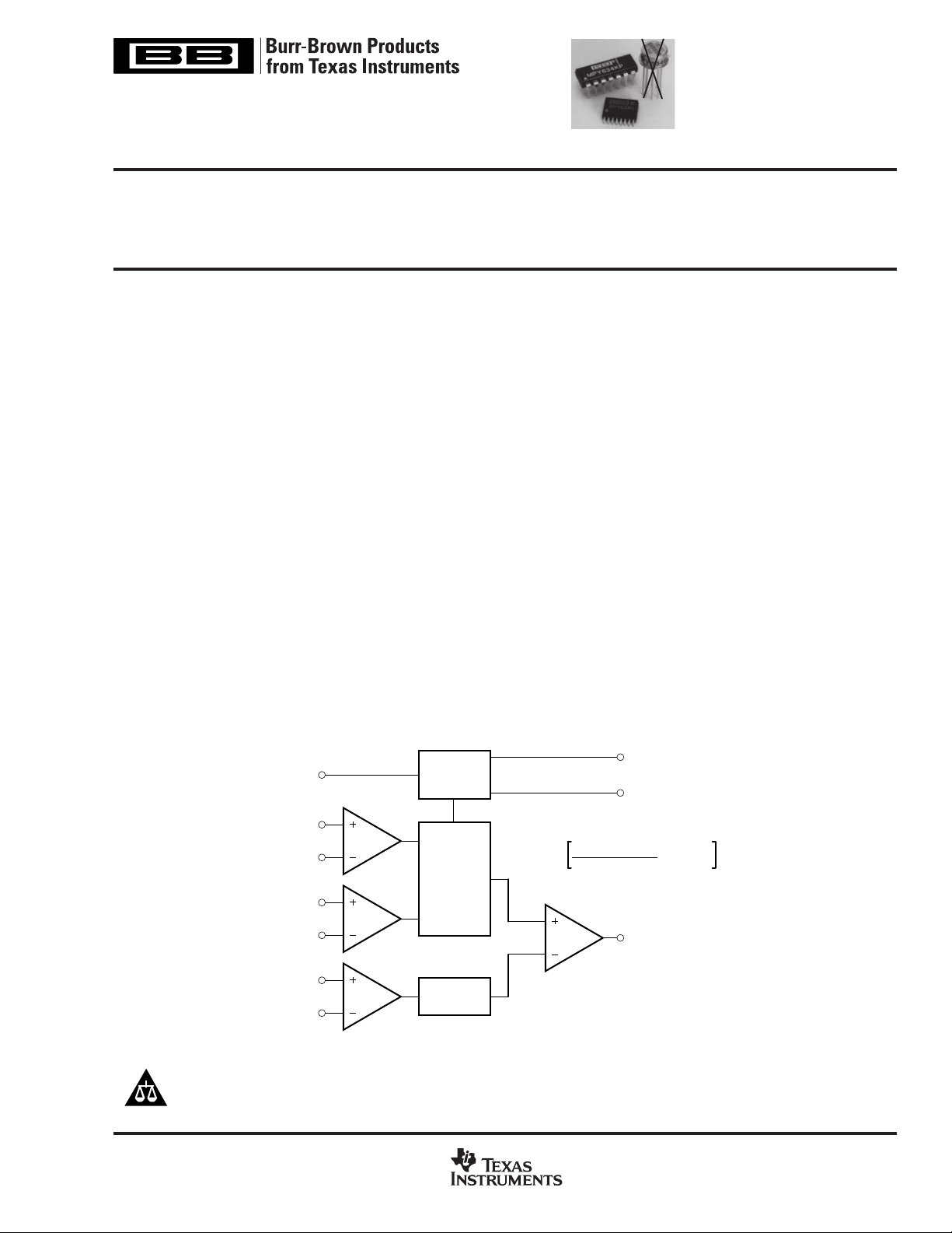
SF
Voltage
Reference
and Bias
DESCRIPTION
The MPY634 is a wide bandwidth, high accuracy, fourquadrant analog multiplier. Its accurately laser-trimmed
multiplier characteristics make it easy to use in a wide
variety of applications with a minimum of external parts,
often eliminating all external trimming. Its differential X, Y,
and Z inputs allow configuration as a multiplier, squarer,
divider, square-rooter, and other functions while maintaining high accuracy.
The wide bandwidth of this new design allows signal
processing at IF, RF, and video frequencies. The internal
output amplifier of the MPY634 reduces
design complexity compared to other high frequency multipliers and balanced modulator circuits. It is
capable of performing frequency mixing, balanced modulation, and demodulation with excellent carrier rejection.
An accurate internal voltage reference provides
precise setting of the scale factor. The differential Z input
allows user-selected scale factors from 0.1 to 10 using
external feedback resistors.
+V
S
–V
S
X
1
X
2
Y
1
Y
2
Z
1
Z
2
Please be aware that an important notice concerning availability, standard warranty, and use in critical applications of
Texas Instruments semiconductor products and disclaimers thereto appears at the end of this data sheet.
All trademarks are the property of their respective owners.
PRODUCTION DATA information is current as of publication date.
Products conform to specifications per the terms of Texas Instruments
standard warranty. Production processing does not necessarily include
testing of all parameters.
V-I
V-I
V-I
Multiplier
Core
0.75 Atten
V
OUT
www.ti.com
Transfer Function
(X1 – X2)(Y1 – Y2)
= A – (Z1 – Z2)
A
SF
V
OUT
Precision
Output
Op Amp
Copyright © 1995-2004, Texas Instruments Incorporated
Page 2
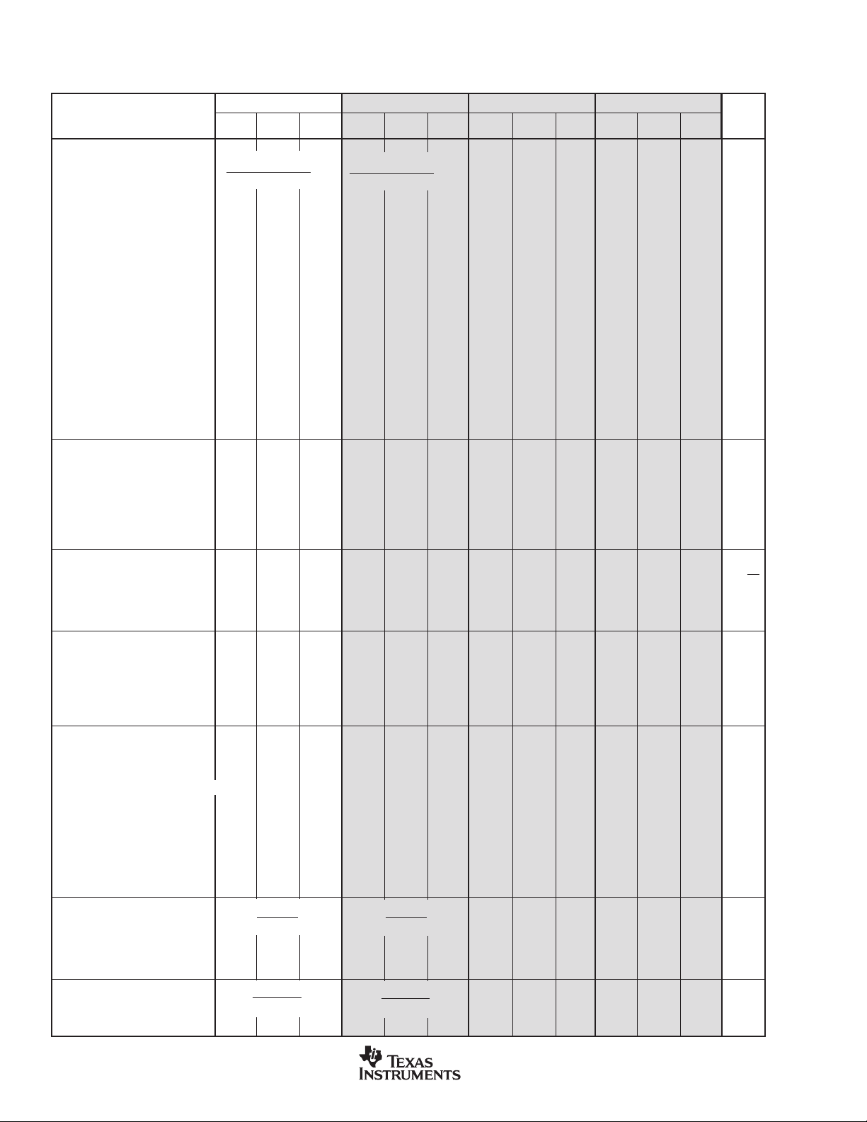
SPECIFICATIONS
ELECTRICAL
At TA = +25°C and VS = ±15VDC, unless otherwise noted.
MPY634KP/KU MPY634AM MPY634BM MPY634SM
MODEL MIN TYP MAX MIN TYP MAX MIN TYP MAX MIN TYP MAX UNITS
OBSOLETE
OBSOLETE
MULTIPLIER
PERFORMANCE
Transfer Function **
Total Error
(1)
(X1 – X2) (Y1 – Y2)
10V
+ Z
2
(X1 – X2) (Y1 – Y2)
10V
+ Z
2
(–10V ≤ X, Y ≤ +10V) ±2.0 ±1.0 ±0.5 * %
T
= min to max ±2.5 ±1.5 ±1.0 ±2.0 %
A
Total Error vs Temperature ±0.03 ±0.022 ±0.015 ±0.02 %/°C
Scale Factor Error
(SF = 10.000V Nominal)
(2)
±0.25 ±0.1 * * %
Temperature Coefficient of
Scaling Voltage ±0.02 ±0.01 ±0.01 * %/°C
Supply Rejection (±15V ±1V) ±0.01 ±0.01 * * %
Nonlinearity
X (X = 20Vp-p, Y = 10V) ±0.4 ±0.4 0.2 ±0.3 * %
Y (Y = 20Vp-p, X = 10V) ±0.01 ±0.01 * ±0.1 * %
Feedthrough
(3)
X (Y Nulled, X = 20Vp-p, 50Hz) ±0.3 ±0.3 ±0.15 ±0.3 * %
Y (X Nulled, Y = 20Vp-p, 50Hz) ±0.01 ±0.01 * ±0.1 * %
Both Inputs (500kHz, 1Vrms)
Unnulled 40 50 45 55 * 60 * * dB
Nulled 556055656070**dB
Output Offset Voltage ±50 ±100 ±5 ±30 * ±15 * * mV
Output Offset Voltage Drift * ±200 ±100 * ±500 µV/°C
DYNAMICS
Small Signal BW,
(V
= 0.1Vrms) 6 10 8 10 * * 6 * MHz
OUT
1% Amplitude Error
(C
= 1000pF) 100 100 * * kHz
LOAD
Slew Rate (V
Settling Time
(to 1%, ∆V
= 20Vp-p) 20 20 * * V/µs
OUT
= 20V) 2 2 * * µs
OUT
NOISE
Noise Spectral Density:
SF = 10V 0.8 0.8 * * µV/√Hz
Wideband Noise:
f = 10Hz to 5MHz 1 1 * * mVrms
f = 10Hz to 10kHz 90 90 * * µVrms
OUTPUT
Output Voltage Swing ±11 ±11 * * V
Output Impedance (f ≤ 1kHz) 0.1 0.1 * * Ω
Output Short Circuit Current
(R
= 0, TA = min to max) 30 30 * * mA
L
Amplifier Open Loop Gain
(f = 50Hz) 85 85 * * dB
INPUT AMPLIFIERS (X, Y and Z)
Input Voltage Range
Differential V
Common-Mode V
(see Typical Performance Curves)
(VCM = 0) ±12 ±12 * * V
IN
(V
= 0) ±10 ±10 * * V
IN
DIFF
Offset Voltage X, Y ±25 ±100 ±5 ±20 ±2 ±10 * * mV
Offset Voltage Drift X, Y 200 100 50 * µV/°C
Offset Voltage Z ±25 ±100 ±5 ±30 ±2 ±15 * * mV
Offset Voltage Drift Z 200 200 100 500 µV/°C
CMRR 60 80 60 80 70 90 * * dB
Bias Current 0.8 2.0 0.8 2.0 * * * * µA
Offset Current 0.1 0.1 * * 2.0 µA
Differential Resistance 10 10 * * MΩ
DIVIDER PERFORMANCE
Transfer Function (X
Total Error
(1)
> X2) **
1
untrimmed
(Z2 – Z1)
10V + Y
(X1 – X2)
(Z2 – Z1)
1
10V + Y
(X1 – X2)
1
(X = 10V, –10V ≤ Z ≤ +10V) 1.5 ±0.75 ±0.35 ±0.75 %
(X = 1V, –1V ≤ Z ≤ +1V) 4.0 ±2.0 ±1.0 * %
(0.1V≤ X ≤ 10V, –10V ≤ Z ≤ 10V) 5.0 ±2.5 ±1.0 * %
SQUARE PERFORMANCE
Transfer Function **
(X1 – X2)
10V
2
+ Z
2
(X1 – X2)
10V
2
+ Z
2
Total Error (–10V ≤ X ≤ 10V) ±1.2 ±0.6 ±0.3 * %
OBSOLETE
2
www.ti.com
MPY634
SBFS017A
Page 3
SPECIFICATIONS (CONT)
ELECTRICAL
At TA = +25°C and VS = ±15VDC, unless otherwise noted.
MPY634KP/KU MPY634AM MPY634BM MPY634SM
MODEL MIN TYP MAX MIN TYP MAX MIN TYP MAX MIN TYP MAX UNITS
SQUARE-ROOTER
PERFORMANCE
Transfer Function (Z
Total Error
POWER SUPPLY
Supply Voltage:
Supply Current, Quiescent 4 6 4 6 * * * * mA
TEMPERATURE RANGE
Specification –40 +85 –25 +85 * * –55 +125 °C
Storage –40 +85 –65 +150 * * * * °C
* Specification same as for MPY634AM.
Gray indicates obsolete parts.
NOTES: (1) Figures given are percent of full scale, ±10V (i.e., 0.01% = 1mV). (2) May be reduced to 3V using external resistor between –V
component due to nonlinearity; excludes effect of offsets.
(1)
Rated Performance ±15 ±15 * * VDC
Operating ±8 ±18 ±8 ±18 * * * ±20 VDC
≤ Z2) **
1
(1V ≤ Z ≤ 10V) ±2.0 ±1.0 ±0.5 * %
√10V (Z2 – Z1) +X
OBSOLETE
2
√10V (Z2 – Z1) +X
OBSOLETE
2
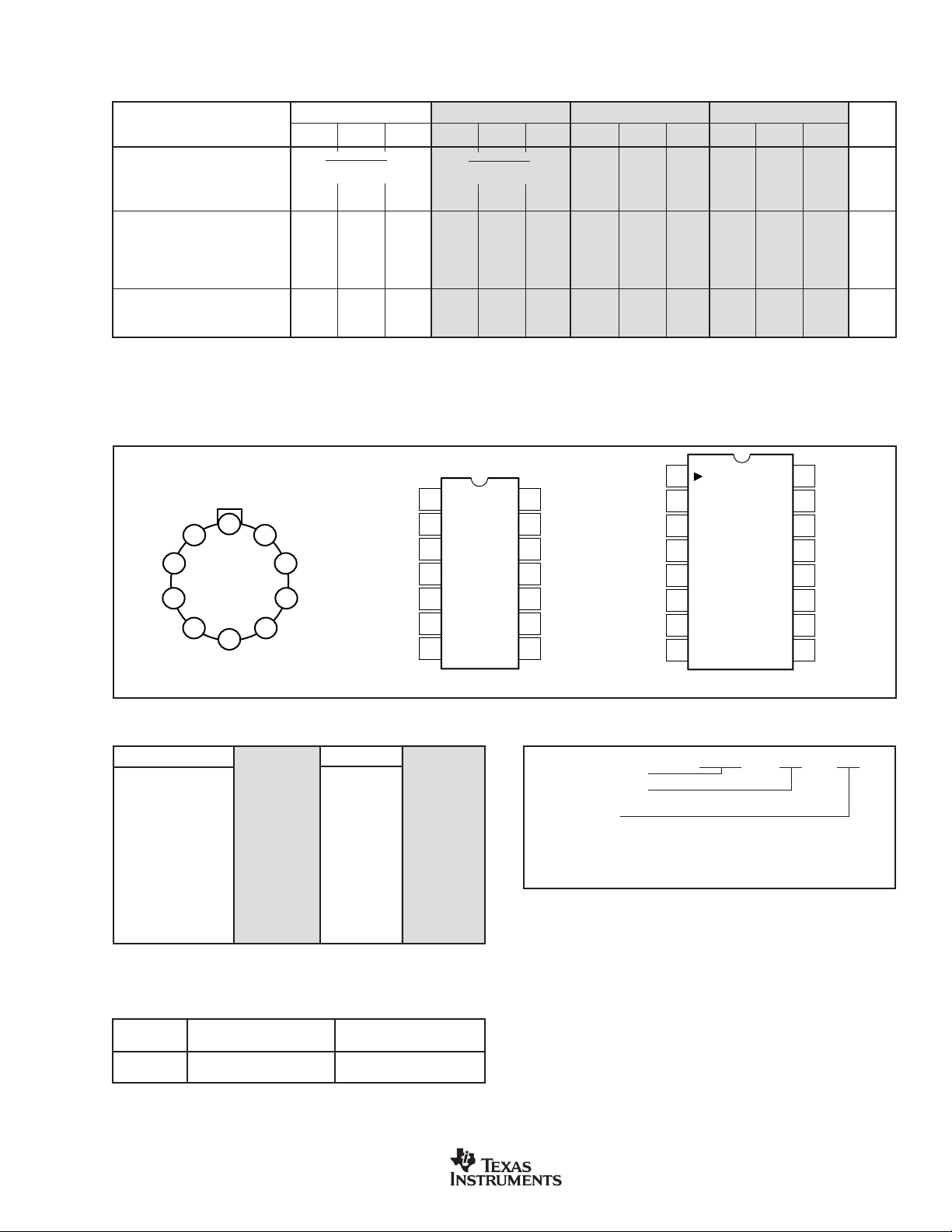
PIN CONFIGURATIONS
OBSOLETE
and SF. (3) Irreducible
S
Top View
X
1
X
2
SF
2
Y
3
1
OBSOLETE
Y
TO-100: MPY634AM/BM/SM
10
1
4
2
5
–V
+V
S
9
8
7
6
Z
2
S
Out
Z
X
X
Scale Factor
1
Y
Y
Input
1
Input
2
Input
1
Input
2
NC
NC
1
2
3
4
5
6
7
ABSOLUTE MAXIMUM RATINGS
PARAMETER MPY634AM/BM MPY634KP/KU MPY634SM
Power Supply Voltage ±18 * ±20
Power Dissipation 500mW * *
Output Short-Circuit
to Ground Indefinite * *
Input Voltage ( all X,
Y and Z) ±V
Temperature Range:
Operating –25°C/+85°C –40°C/+85°C –55°C/+125°C
Storage –65°C/+150°C –40°C/+85°C*
Lead Temperature
(soldering, 10s) +300°C* *
SOIC ‘KU’ Package +260°C
* Specification same as for MPY634AM/BM.
NOTE: Gray indicates obsolete parts.
OBSOLETE OBSOLETE
S
**
1
1
2
Input
NC
NC
Input
Input
NC
1
2
3
4
5
6
7
8
SOIC: MPY634KUDIP: MPY634KP
X
14
+V
S
13
NC
12
Output
11
Z
Input
1
10
Z
Input
2
9
NC
8
–V
S
X2 Input
Scale Factor
Y
Y
16
+V
S
15
NC
14
Output
13
Z
Input
1
12
Z
Input
2
11
NC
10
–V
S
9
NC
ORDERING INFORMATION
Basic Model Number
Performance Grade
K: U: –40°C to +85°C
Package Code
P: Plastic 14-pin DIP
U: 16-pin SOIC
NOTE: (1) Performance grade identifier may not be marked on the SOIC
package; a blank denotes “K” grade.
(1)
MPY634 ( )( )
PACKAGE INFORMATION
PRODUCT PACKAGE NUMBER
MPY634KP 14-Pin PDIP 010
MPY634KU 16-Pin SOIC 211
NOTE: (1) For the most current package and ordering information, see the
Package Option Addendum located at the end of this data sheet.
(1)
PACKAGE DRAWING
MPY634
SBFS017A
www.ti.com
3
Page 4
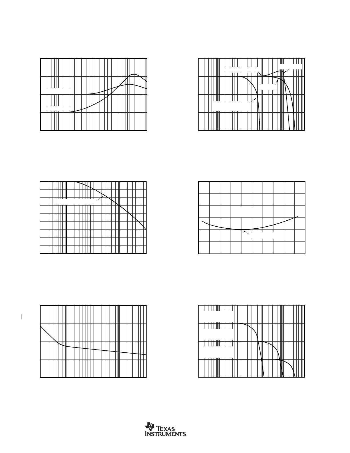
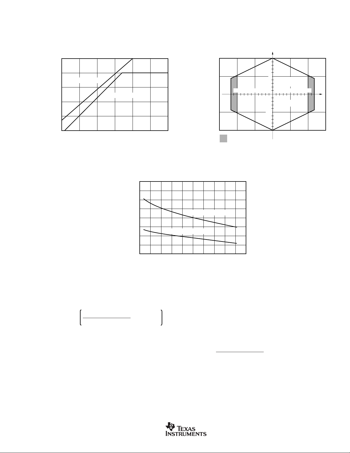
TYPICAL PERFORMANCE CURVES
At TA = +25°C, VS = ±15VDC, unless otherwise noted.
–20
FEEDTHROUGH vs FREQUENCY
–40
X Feedthrough
–60
Y Feedthrough
–80
Feedthrough Attenuation (dB)
–100
100 1k 10k 1M 10M 100M
100k
Frequency (Hz)
COMMON-MODE REJECTION RATIO vs FREQUENCY
90
80
70
60
Typical for all inputs
50
40
CMRR (dB)
30
20
10
0
100 100M
10k 1M 10M
Frequency (Hz)
10
FREQUENCY RESPONSE AS A MULTIPLIER
Normal Connection
0
CL = 0pF
–10
With X10 Feedback
–20
Output Response (dB)
Attenuator
–30
1k 10k 100k 1M 10M 100M
Frequency (Hz)
FEEDTHROUGH vs TEMPERATURE
–50
–60
fY = 500kHz
V
= nulled
X
–70
nulled at 25°C
Feedthrough Attenuation (dB)
–80
–60
–20 20 60 100 140–40 0 40 80 120
Temperature (°C)
C
= 1000pF
L
NOISE SPECTRAL DENSITY
1.5
1.25
1
0.75
Noise Spectral Density (µV/√Hz)
0.5
10 100 10k 100k
vs FREQUENCY
1k
Frequency (Hz)
4
www.ti.com
60
FREQUENCY RESPONSE AS A DIVIDER
VX = 100mVDC
V
= 10mVrms
40
(dB)
2
/V
0
20
Output, V
Z
= 1VDC
V
X
V
= 100mVrms
Z
= 10VDC
V
X
V
= 100mVrms
Z
0
–20
1k 10k 100k 1M 10M 100M
Frequency (Hz)
MPY634
SBFS017A
Page 5
TYPICAL PERFORMANCE CURVES (CONT)
TA = +25°C, VS = ±15VDC, unless otherwise noted.
INPUT/OUTPUT SIGNAL RANGE
vs SUPPLY VOLTAGES
14
INPUT DIFFERENTIAL-MODE/
COMMON-MODE VOLTAGE
10
V
CM
12
Output, RL ≥ 2kΩ
10
All inputs, SF = 10V
8
6
Peak Positive or Negative Signal (V)
4
81012 161820
Positive or Negative Supply (V)
14
Bias Current (nA)
800
700
600
500
400
300
200
100
BIAS CURRENTS vs TEMPERATURE
0
–60
–20 0 60 100 140
(X,Y or Z Inputs)
Scaling Voltage = 10V
Scaling Voltage = 3V
20–40 40 80 120
Temperature (°C)
5
Specified
Accuracy
–12 12
Functional
Derated Accuracy
–5510–10
VS = ±15V
–5
–10
V
DIFF
THEORY OF OPERATION
The transfer function for the MPY634 is:
V
OUT
where:
A = open-loop gain of the output amplifier (typically
85dB at DC).
SF = Scale Factor. Laser-trimmed to 10V but adjustable
over a 3V to 10V range using external resistors.
X, Y, Z are input voltages. Full-scale input voltage
is equal to the selected SF. (Max input voltage =
±1.25 SF).
An intuitive understanding of transfer function can be gained
by analogy to the op amp. By assuming that the open-loop
gain, A, of the output operational amplifier is infinite,
MPY634
SBFS017A
(X1 – X2) (Y1 – Y2)
= A – (Z1 – Z2)
SF
www.ti.com
inspection of the transfer function reveals that any V
OUT
can
be created with an infinitesimally small quantity within the
brackets. Then, an application circuit can be analyzed by
assigning circuit voltages for all X, Y and Z inputs and
setting the bracketed quantity equal to zero. For example,
the basic multiplier connection in Figure 1, Z1 = V
OUT
and
Z2 = 0. The quantity within the brackets then reduces to:
(X1 – X2) (Y1 – Y2)
– (V
SF
OUT
– 0) = 0
This approach leads to a simple relationship which can be
solved for V
to provide the closed-loop transfer function.
OUT
The scale factor is accurately factory adjusted to 10V and is
typically accurate to within 0.1% or less. The scale factor
may be adjusted by connecting a resistor or potentiometer
between pin SF and the –VS power supply. The value of the
external resistor can be approximated by:
5
Page 6
RSF = 5.4kΩ
SF
10 – SF
Internal device tolerances make this relationship accurate to
within approximately 25%. Some applications can benefit
from reduction of the SF by this technique. The reduced
input bias current, noise, and drift achieved by this technique
can be likened to operating the input circuitry in a higher
gain, thus reducing output contributions to these effects.
Adjustment of the scale factor does not affect bandwidth.
The MPY634 is fully characterized at V
= ±15V but
S
operation is possible down to ±8V with an attendant reduction of input and output range capability. Operation at
voltages greater than ±15V allows greater output swing to be
achieved by using an output feedback attenuator (Figure 1).
As with any wide bandwidth circuit, the power supplies
should be bypassed with high frequency ceramic capacitors.
These capacitors should be located as near as practical to the
power supply connections of the MPY634. Improper bypassing can lead to instability, overshoot, and ringing in the
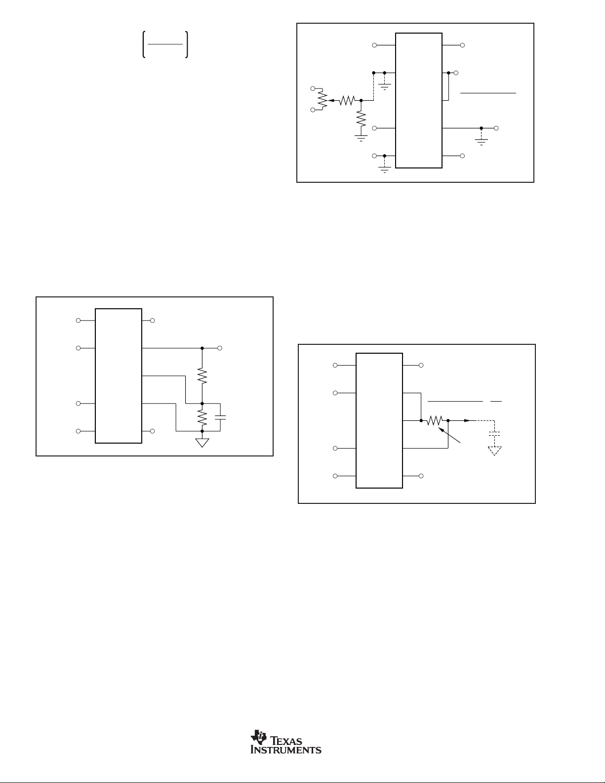
output.
X Input
±10V FS
±12V PK
Y Input
±10V FS
±12V PK
+V
X
1
X
Out
2
MPY634
SF Z
Y
1
Y
–V
2
+15V
S
1
Z
2
–15V
S
10kΩ
V
, ±12V PK
OUT
= (X
– X2) (Y1 – Y2)
1
(Scale = 1V)
90kΩ
Optional
Peaking
Capacitor
C
= 200pF
F
FIGURE 1. Connections for Scale-Factor of Unity.
BASIC MULTIPLIER CONNECTION
Figure 2 shows the basic connection as a multiplier. Accuracy is fully specified without any additional user-trimming
circuitry. Some applications can benefit from trimming of
one or more of the inputs. The fully differential inputs
facilitate referencing the input quantities to the source voltage common terminal for maximum accuracy. They also
allow use of simple offset voltage trimming circuitry as
shown on the X input.
The differential Z input allows an offset to be summed in
V
. In basic multiplier operation, the Z2 input serves as
OUT
the output voltage ground reference and should be connected
to the ground of the driven system for maximum accuracy.
A method of changing (lowering) SF by connecting to the
SF pin was discussed previously. Figure 1 shows an alternative method of changing the effective SF of the overall
circuit by using an attenuator in the feedback connection to
Z1. This method puts the output amplifier in a higher gain
and is thus accompanied by a reduction in bandwidth and an
+15V
V
OUT
– X2) (Y1 – Y2)
(X
1
=
–15V
, ±12V PK
10V
Optional
Summing
Z, ±10V PK
+ Z2
Input,
+15V
50kΩ
–15V
Optional Offset
Trim Circuit
X Input
±10V FS
±12V PK
470kΩ
Y Input
±10V FS
±12V PK
1kΩ
+V
X
1
X
Out
2
MPY634
SF Z
Y
1
Y
–V
2
S
1
Z
2
S
FIGURE 2. Basic Multiplier Connection.
increase in output offset voltage. The larger output offset
may be reduced by applying a trimming voltage to the high
impedance input, Z
.
2
The flexibility of the differential Z inputs allows direct
conversion of the output quantity to a current. Figure 3
shows the output voltage differentially-sensed across a series resistor forcing an output-controlled current. Addition
of a capacitor load then creates a time integration function
useful in a variety of applications such as power computation.
X Input
±10V FS
±12V PK
Y Input
±10V FS
±12V PK
+V
X
1
X
Out
2
MPY634
SF Z
Y
1
Y
–V
2
S
1
Z
2
S
+15V
I
=
OUT
– X2) (Y1 – Y2)
(X
1
x
10V
Current
Sensing
Resistor,
R
, 2kΩ
–15V
S
min
1
R
S
Integrator
Capacitor
(see text)
FIGURE 3. Conversion of Output to Current.
SQUARER CIRCUIT (FREQUENCY DOUBLER)
Squarer, or frequency doubler, operation is achieved by
paralleling the X and Y inputs of the standard multiplier
circuit. Inverted output can be achieved by reversing the
differential input terminals of either the X or Y input.
Accuracy in the squaring mode is typically a factor of two
better than the specified multiplier mode with maximum
error occurring with small (less than 1V) inputs. Better
accuracy can be achieved for small input voltage levels by
reducing the scale factor, SF.
DIVIDER OPERATION
The MPY634 can be configured as a divider as shown in
Figure 4. High impedance differential inputs for the numerator and denominator are achieved at the Z and X inputs,
Hello
6
www.ti.com
MPY634
SBFS017A
Page 7

respectively. Feedback is applied to the Y2 input, and Y1 is
g
normally referenced to output ground. Alternatively, as the
transfer function implies, an input applied to Y1 can be
summed directly into V
. Since the feedback connection
OUT
is made to a multiplying input, the effective gain of the
output op amp varies as a function of the denominator input
voltage. Therefore, the bandwidth of the divider function is
proportional to the denominator voltage (see Typical Performance Curves).
Output, ±12V PK
+15V
V
= + Y1
OUT
Z Input
(Numerator)
±10V FS,
±12V PK
10V(Z
(X1 – X2)
2
– Z1)
X Input
(Denominator)
0.1V ≤ X ≤ 10V
Optional
Summing Input
±10V PK
+
–
+V
X
1
X
Out
2
MPY634
SF Z
Y
1
S
1
Z
2
+15V
+V
X
Optional
Summing
Input, X,
±10V PK
1
X
2
SF Z
Y
1
Y
2
MPY634
Out
–V
S
1
Z
2
S
Z Input
10V FS
12V PK
–15V
FIGURE 5. Square-Rooter Connection.
APPLICATIONS
Output, ±12V PK
V
= 10V(Z2 – Z1) + X
OUT
Reverse
this and
X inputs
for
Negative
Outputs
R
L
(Must be
provided)
2
Y
–V
2
S
–15V
FIGURE 4. Basic Divider Connection.
Accuracy of the divider mode typically ranges from 1.0% to
2.5% for a 10 to 1 denominator range depending on device
grade. Accuracy is primarily limited by input offset voltages
and can be significantly improved by trimming the offset of
the X input. A trim voltage of ±3.5mV applied to the “low
side” X input (X2 for positive input voltages on X1) can
produce similar accuracies over 100 to 1 denominator range.
To trim, apply a signal which varies from 100mV to 10V at
a low frequency (less than 500Hz). An offset sine wave or
ramp is suitable. Since the ratio of the quantities should be
constant, the ideal output would be a constant 10V. Using
AC coupling on an oscilloscope, adjust the offset control for
minimum output voltage variation.
SQUARE-ROOTER
A square-rooter connection is shown in Figure 5. Input
voltage is limited to one polarity (positive for the connection
shown). The diode prevents circuit latch-up should the input
go negative. The circuit can be configured for negative input
and positive output by reversing the polarity of both the X
and Y inputs. The output polarity can be reversed by reversing the diode and X input polarity. A load resistance of
approximately 10kΩ must be provided. Trimming for improved accuracy would be accomplished at the Z input.
A sin (2π 10MHz t)
B sin (2π 10MHz t + )
Multiplier connection followed by a low-pass filter forms phase
detector useful in phase-locked-loop circuitry. R
PLL circuitry to provide desired loop-dampin
θ
+V
X
1
X
2
MPY634
SF Z
Y
1
Y
–V
2
Out
S
1
Z
2
S
+15V
1kΩ
–15V
X
characteristics.
FIGURE 6. Phase Detector.
+15V
–15V
+
E
C
–
2kΩ 2kΩ
+
E
S
–
+V
X
1
X
2
MPY634
SF Z
Y
1
Y
–V
2
S
V
O
1
Z
2
S
–15V
V
= (AB/20) cos
O
0.1µF
R
X
is often used in
VO = 10 • E
OPA606
A
1
39kΩ
1kΩ
C
θ
• ES
MPY634
SBFS017A
Minor gain adjustments are accomplished with the 1kΩ variable resistor
connected to the scale factor adjustment pin, SF. Bandwidth of this circuit
is limited by A
, which is operated at relatively high gain.
1
FIGURE 7. Voltage-Controlled Amplifier.
www.ti.com
7
Page 8

18kΩ
y
10kΩ
Input, E
0 to +10V
θ
X
+V
1
X
Out
2
MPY634
SF Z
Y
1
Y
–V
2
S
1
Z
2
S
4.7kΩ
4.3kΩ
–15V
+15V
V
OUT
Where
θ
= (π/2) (E /10V)
3kΩ
= (10V) sin
With a linearly changing 0-10V input, this circuit’s output follows
0° to 90° of a sine function with a 10V peak output amplitude.
Modulation
Input, ±E
M
θ
θ
Carrier Input
E
sin ωt
C
+V
X
1
X
Out
2
MPY634
SF Z
Y
1
Y
–V
2
S
1
Z
2
S
–15V
+15V
V
OUT
1 ± (E
=
/10V) EC sin ωt
M
By injecting the input carrier signal into the output through connection
to the Z
input, conventional amplitude modulation is achieved.
2
Amplification can be achieved by use of the SF pin, or Z attenuator
(at the expense of bandwidth).
FIGURE 9. Linear AM Modulator.FIGURE 8. Sine-Function Generator.
A sin ω t
Squaring a sinusoidal input creates an output frequency of
twice that of the input. The DC output component is
removed b
AC-coupling the output.
FIGURE 10. Frequency Doubler.
Modulation
Input, ±E
M
470kΩ
Carrier
Null
+15V –15V
Carrier Input
E
C
1kΩ
sin ω t
X
1
X
2
MPY634
SF Z
Y
1
Y
2
+V
X
1
X
2
MPY634
SF Z
Y
1
Y2–V
Out
+V
S
+15V
(A2/20) cos (2 ω t)
Out
C
R
–V
1
Z
2
S
–15V
Frequency Doubler
Input Signal: 20Vp-p, 200kHz
Output Signal: 10Vp-p, 400kHz
+15V
S
V
OUT
1
Z
2
S
–15V
The basic muliplier connection performs balanced modulation.
Carrier rejection can be improved by trimming the offset voltage
of the modulation input. Better carrier rejection above 2MHz is
typically achieved by interchanging the X and Y inputs (carrier
applied to the X input).
FIGURE 11. Balanced Modulator.
8
www.ti.com
Carrier: fC = 2MHz, Amplitude = 1Vrms
Signal: f
= 120kHz, Amplitude = 10V peak
S
MPY634
SBFS017A
Page 9

PACKAGE OPTION ADDENDUM
www.ti.com
11-Apr-2015
PACKAGING INFORMATION
Orderable Device Status
MPY634AM OBSOLETE TO-100 LME 10 TBD Call TI Call TI
MPY634BM OBSOLETE TO-100 LME 10 TBD Call TI Call TI
MPY634KP ACTIVE PDIP N 14 25 Green (RoHS
MPY634KPG4 ACTIVE PDIP N 14 25 Green (RoHS
MPY634KU ACTIVE SOIC DW 16 40 Green (RoHS
MPY634KU/1K ACTIVE SOIC DW 16 1000 Green (RoHS
MPY634KU/1KE4 ACTIVE SOIC DW 16 1000 Green (RoHS
MPY634KUE4 ACTIVE SOIC DW 16 40 Green (RoHS
(1)
The marketing status values are defined as follows:
ACTIVE: Product device recommended for new designs.
LIFEBUY: TI has announced that the device will be discontinued, and a lifetime-buy period is in effect.
NRND: Not recommended for new designs. Device is in production to support existing customers, but TI does not recommend using this part in a new design.
PREVIEW: Device has been announced but is not in production. Samples may or may not be available.
OBSOLETE: TI has discontinued the production of the device.
Package Type Package
(1)
Drawing
Pins Package
Qty
Eco Plan
(2)
& no Sb/Br)
& no Sb/Br)
& no Sb/Br)
& no Sb/Br)
& no Sb/Br)
& no Sb/Br)
Lead/Ball Finish
(6)
CU NIPDAU N / A for Pkg Type MPY634KP
CU NIPDAU N / A for Pkg Type MPY634KP
CU NIPDAU-DCC Level-3-260C-168 HR -40 to 85 MPY634U
CU NIPDAU-DCC Level-3-260C-168 HR -40 to 85 MPY634U
CU NIPDAU-DCC Level-3-260C-168 HR -40 to 85 MPY634U
CU NIPDAU-DCC Level-3-260C-168 HR -40 to 85 MPY634U
MSL Peak Temp
(3)
Op Temp (°C) Device Marking
(4/5)
(2)
Eco Plan - The planned eco-friendly classification: Pb-Free (RoHS), Pb-Free (RoHS Exempt), or Green (RoHS & no Sb/Br) - please check http://www.ti.com/productcontent for the latest availability
information and additional product content details.
TBD: The Pb-Free/Green conversion plan has not been defined.
Pb-Free (RoHS): TI's terms "Lead-Free" or "Pb-Free" mean semiconductor products that are compatible with the current RoHS requirements for all 6 substances, including the requirement that
lead not exceed 0.1% by weight in homogeneous materials. Where designed to be soldered at high temperatures, TI Pb-Free products are suitable for use in specified lead-free processes.
Pb-Free (RoHS Exempt): This component has a RoHS exemption for either 1) lead-based flip-chip solder bumps used between the die and package, or 2) lead-based die adhesive used between
the die and leadframe. The component is otherwise considered Pb-Free (RoHS compatible) as defined above.
Green (RoHS & no Sb/Br): TI defines "Green" to mean Pb-Free (RoHS compatible), and free of Bromine (Br) and Antimony (Sb) based flame retardants (Br or Sb do not exceed 0.1% by weight
in homogeneous material)
(3)
MSL, Peak Temp. - The Moisture Sensitivity Level rating according to the JEDEC industry standard classifications, and peak solder temperature.
(4)
There may be additional marking, which relates to the logo, the lot trace code information, or the environmental category on the device.
Samples
Addendum-Page 1
Page 10

PACKAGE OPTION ADDENDUM
www.ti.com
11-Apr-2015
(5)
Multiple Device Markings will be inside parentheses. Only one Device Marking contained in parentheses and separated by a "~" will appear on a device. If a line is indented then it is a continuation
of the previous line and the two combined represent the entire Device Marking for that device.
(6)
Lead/Ball Finish - Orderable Devices may have multiple material finish options. Finish options are separated by a vertical ruled line. Lead/Ball Finish values may wrap to two lines if the finish
value exceeds the maximum column width.
Important Information and Disclaimer:The information provided on this page represents TI's knowledge and belief as of the date that it is provided. TI bases its knowledge and belief on information
provided by third parties, and makes no representation or warranty as to the accuracy of such information. Efforts are underway to better integrate information from third parties. TI has taken and
continues to take reasonable steps to provide representative and accurate information but may not have conducted destructive testing or chemical analysis on incoming materials and chemicals.
TI and TI suppliers consider certain information to be proprietary, and thus CAS numbers and other limited information may not be available for release.
In no event shall TI's liability arising out of such information exceed the total purchase price of the TI part(s) at issue in this document sold by TI to Customer on an annual basis.
Addendum-Page 2
Page 11
PACKAGE MATERIALS INFORMATION
www.ti.com 14-Jul-2012
TAPE AND REEL INFORMATION
*All dimensions are nominal
Device Package
MPY634KU/1K SOIC DW 16 1000 330.0 16.4 10.75 10.7 2.7 12.0 16.0 Q1
Type
Package
Drawing
Pins SPQ Reel
Diameter
(mm)
Reel
Width
W1 (mm)
A0
(mm)B0(mm)K0(mm)P1(mm)W(mm)
Pin1
Quadrant
Pack Materials-Page 1
Page 12

PACKAGE MATERIALS INFORMATION
www.ti.com 14-Jul-2012
*All dimensions are nominal
Device Package Type Package Drawing Pins SPQ Length (mm) Width (mm) Height (mm)
MPY634KU/1K SOIC DW 16 1000 367.0 367.0 38.0
Pack Materials-Page 2
Page 13

MECHANICAL DATA
MMBC006 – MARCH 2001
LME (O–MBCY–W10) MET AL CYLINDRICAL PACKAGE
0.370 (9,40)
ø
0.335 (8,51)
0.335 (8,51)
ø
0.305 (7,75)
0.040 (1,02)
0.010 (0,25)
0.040 (1,02)
0.010 (0,25)
0.185 (4,70)
0.165 (4,19)
Seating
Plane
0.021 (0,53)
ø
0.016 (0,41)
0.160 (4,06)
ø
0.120 (3,05)
0.034 (0,86)
36
0.028 (0,71)
NOTES: A. All linear dimensions are in inches (millimeters).
B. This drawing is subject to change without notice.
C. Leads in true position within 0.010 (0,25) R @ MMC at seating plane.
D. Pin numbers shown for reference only. Numbers may not be marked on package.
E. Falls within JEDEC MO–006/TO-100.
0.500 (12,70) MIN
0.120 (3,05)
0.110 (2,79)
4
3
5
2
1
°
10
6
7
0.230 (5,84)
8
9
0.045 (1,14)
0.029 (0,74)
4202488/A 03/01
POST OFFICE BOX 655303 • DALLAS, TEXAS 75265
1
Page 14

Page 15

Page 16

Page 17

IMPORTANT NOTICE
Texas Instruments Incorporated and its subsidiaries (TI) reserve the right to make corrections, enhancements, improvements and other
changes to its semiconductor products and services per JESD46, latest issue, and to discontinue any product or service per JESD48, latest
issue. Buyers should obtain the latest relevant information before placing orders and should verify that such information is current and
complete. All semiconductor products (also referred to herein as “components”) are sold subject to TI’s terms and conditions of sale
supplied at the time of order acknowledgment.
TI warrants performance of its components to the specifications applicable at the time of sale, in accordance with the warranty in TI’s terms
and conditions of sale of semiconductor products. Testing and other quality control techniques are used to the extent TI deems necessary
to support this warranty. Except where mandated by applicable law, testing of all parameters of each component is not necessarily
performed.
TI assumes no liability for applications assistance or the design of Buyers’ products. Buyers are responsible for their products and
applications using TI components. To minimize the risks associated with Buyers’ products and applications, Buyers should provide
adequate design and operating safeguards.
TI does not warrant or represent that any license, either express or implied, is granted under any patent right, copyright, mask work right, or
other intellectual property right relating to any combination, machine, or process in which TI components or services are used. Information
published by TI regarding third-party products or services does not constitute a license to use such products or services or a warranty or
endorsement thereof. Use of such information may require a license from a third party under the patents or other intellectual property of the
third party, or a license from TI under the patents or other intellectual property of TI.
Reproduction of significant portions of TI information in TI data books or data sheets is permissible only if reproduction is without alteration
and is accompanied by all associated warranties, conditions, limitations, and notices. TI is not responsible or liable for such altered
documentation. Information of third parties may be subject to additional restrictions.
Resale of TI components or services with statements different from or beyond the parameters stated by TI for that component or service
voids all express and any implied warranties for the associated TI component or service and is an unfair and deceptive business practice.
TI is not responsible or liable for any such statements.
Buyer acknowledges and agrees that it is solely responsible for compliance with all legal, regulatory and safety-related requirements
concerning its products, and any use of TI components in its applications, notwithstanding any applications-related information or support
that may be provided by TI. Buyer represents and agrees that it has all the necessary expertise to create and implement safeguards which
anticipate dangerous consequences of failures, monitor failures and their consequences, lessen the likelihood of failures that might cause
harm and take appropriate remedial actions. Buyer will fully indemnify TI and its representatives against any damages arising out of the use
of any TI components in safety-critical applications.
In some cases, TI components may be promoted specifically to facilitate safety-related applications. With such components, TI’s goal is to
help enable customers to design and create their own end-product solutions that meet applicable functional safety standards and
requirements. Nonetheless, such components are subject to these terms.
No TI components are authorized for use in FDA Class III (or similar life-critical medical equipment) unless authorized officers of the parties
have executed a special agreement specifically governing such use.
Only those TI components which TI has specifically designated as military grade or “enhanced plastic” are designed and intended for use in
military/aerospace applications or environments. Buyer acknowledges and agrees that any military or aerospace use of TI components
which have not been so designated is solely at the Buyer's risk, and that Buyer is solely responsible for compliance with all legal and
regulatory requirements in connection with such use.
TI has specifically designated certain components as meeting ISO/TS16949 requirements, mainly for automotive use. In any case of use of
non-designated products, TI will not be responsible for any failure to meet ISO/TS16949.
Products Applications
Audio www.ti.com/audio Automotive and Transportation www.ti.com/automotive
Amplifiers amplifier.ti.com Communications and Telecom www.ti.com/communications
Data Converters dataconverter.ti.com Computers and Peripherals www.ti.com/computers
DLP® Products www.dlp.com Consumer Electronics www.ti.com/consumer-apps
DSP dsp.ti.com Energy and Lighting www.ti.com/energy
Clocks and Timers www.ti.com/clocks Industrial www.ti.com/industrial
Interface interface.ti.com Medical www.ti.com/medical
Logic logic.ti.com Security www.ti.com/security
Power Mgmt power.ti.com Space, Avionics and Defense www.ti.com/space-avionics-defense
Microcontrollers microcontroller.ti.com Video and Imaging www.ti.com/video
RFID www.ti-rfid.com
OMAP Applications Processors www.ti.com/omap TI E2E Community e2e.ti.com
Wireless Connectivity www.ti.com/wirelessconnectivity
Mailing Address: Texas Instruments, Post Office Box 655303, Dallas, Texas 75265
Copyright © 2015, Texas Instruments Incorporated
 Loading...