

现货库存、技术资料、百科信息、热点资讯,精彩尽在鼎好!
www.ti.com
20
19
18
17
16
15
14
13
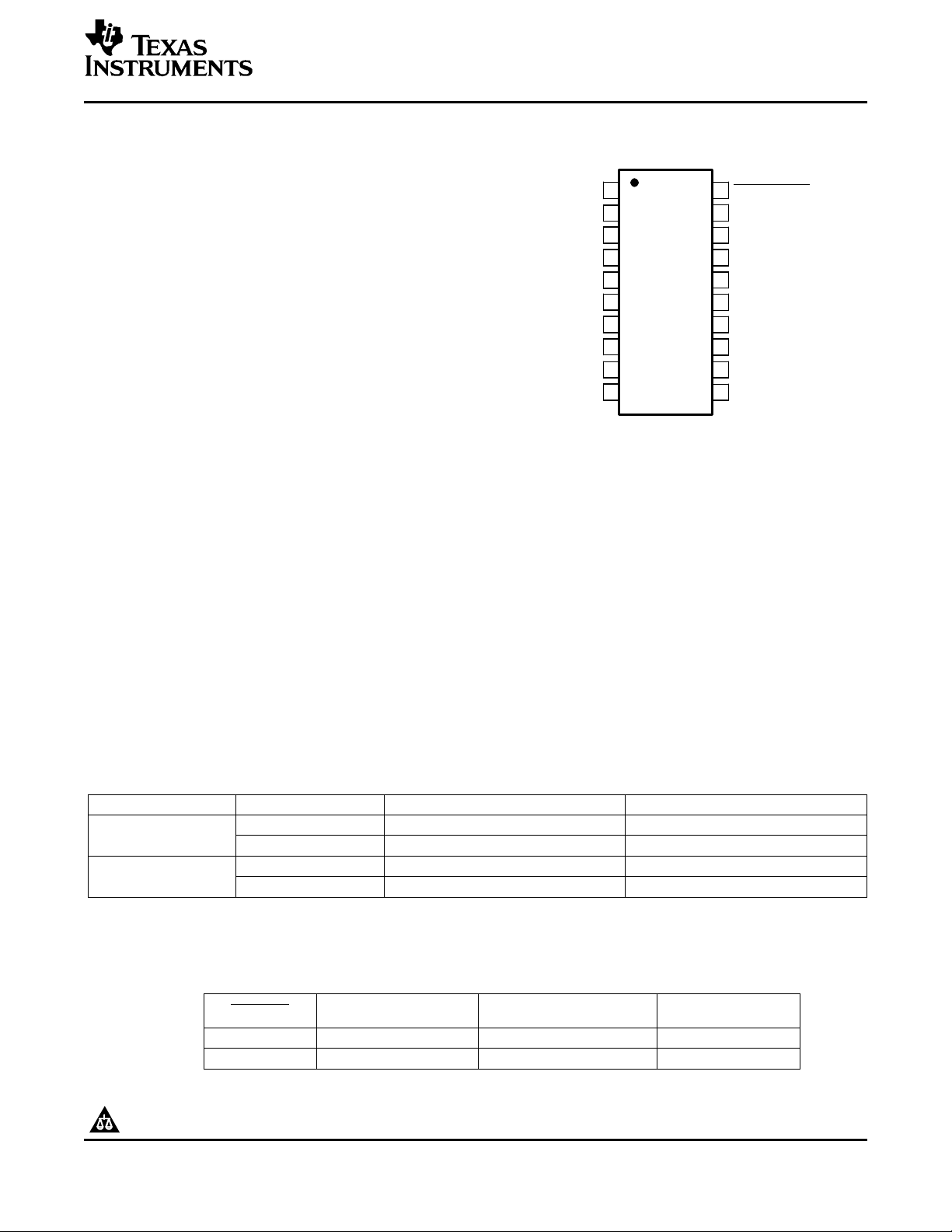
1
2
3
4
5
6
7
8
GND
DOUT1C2+
C1−
V+
C1+
TOP VIEW
DOUT2
RIN1
DIN2
DIN1
V−
C2−
12
11
9
10 ROUT1ROUT2
DIN3
TSSOP OR SSOP PACKAGE
RIN2
DOUT3
V
CC
V
L
PWRDOWN
FEATURES
• V
• Enhanced ESD Protection on RIN Inputs and
• Low 300- µ A Supply Current
• Specified 250-kbps Data Rate
• 1- µ A Low-Power Shutdown
• Meets EIA/TIA-232 Specifications Down
Pin for Compatibility With Mixed-Voltage
L
Systems Down to 1.8 V on Logic Side
DOUT Outputs
– ± 15-kV Human-Body Model
– ± 15-kV IEC 61000-4-2, Air-Gap Discharge
– ± 8-kV IEC 61000-4-2, Contact Discharge
to 3 V
APPLICATIONS
• Hand-Held Equipment
• PDAs
• Cell Phones
• Battery-Powered Equipment
• Data Cables
MAX3386E
RS-232 TRANSCEIVER
WITH SPLIT SUPPLY PIN FOR LOGIC SIDE
SLLS659 – MAY 2006
DESCRIPTION/ORDERING INFORMATION
The MAX3386E is a three-driver and two-receiver RS-232 interface device, with split supply pins for
mixed-signal operations. All RS-232 inputs and outputs are protected to ± 15 kV using the IEC 61000-4-2
Air-Gap Discharge method, ± 8 kV using the IEC 61000-4-2 Contact Discharge method, and ± 15 kV using the
Human-Body Model.
The charge pump requires only four small 0.1- µ F capacitors for operation from a 3.3-V supply. The MAX3386E
is capable of running at data rates up to 250 kbps, while maintaining RS-232-compliant output levels.
The MAX3386E has a unique V
and receiver out (ROUT) logic levels are pin programmable through the V
space-saving thin shrink small-outline package (TSSOP).
0 ° C to 70 ° C
–40 ° C to 85 ° C
(1) Package drawings, standard packing quantities, thermal data, symbolization, and PCB design guidelines are available at
www.ti.com/sc/package.
Please be aware that an important notice concerning availability, standard warranty, and use in critical applications of Texas
Instruments semiconductor products and disclaimers thereto appears at the end of this data sheet.
PRODUCTION DATA information is current as of publication date.
Products conform to specifications per the terms of the Texas
Instruments standard warranty. Production processing does not
necessarily include testing of all parameters.
T
A
pin that allows operation in mixed-logic voltage systems. Both driver in (DIN)
L
pin. The MAX3386E is available in a
L
ORDERING INFORMATION
PACKAGE
TSSOP MAX3386ECPWR MP386EC
SSOP MAX3386ECDBR MAX3386EC
TSSOP MAX3386EIPWR MP386EI
SSOP MAX3386EIDBR MAX3386EI
(1)
ORDERABLE PART NUMBER TOP-SIDE MARKING
TRUTH TABLE (SHUTDOWN FUNCTION)
PWRDWN RECEIVER OUTPUTS CHARGE PUMP
L High-Z High-Z Inactive
H Active Active Active
DRIVER
OUTPUTS
Copyright © 2006, Texas Instruments Incorporated
www.ti.com
DIN2
DOUT3
9 15
Powerdown
RIN1
14
20
11
PWRDOWN
ROUT1
DIN1
DOUT2
8 16
RIN2
1310
ROUT2
DIN1
DOUT1
7 17
5 K
5 K
MAX3386E
RS-232 TRANSCEIVER
WITH SPLIT SUPPLY PIN FOR LOGIC SIDE
SLLS659 – MAY 2006
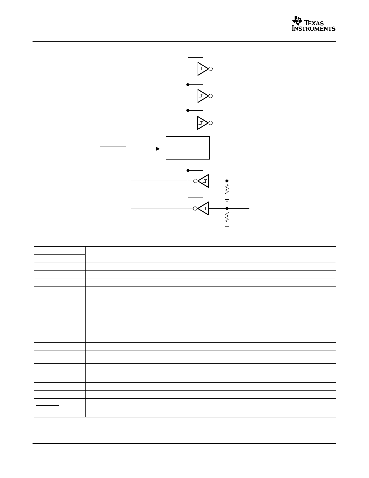
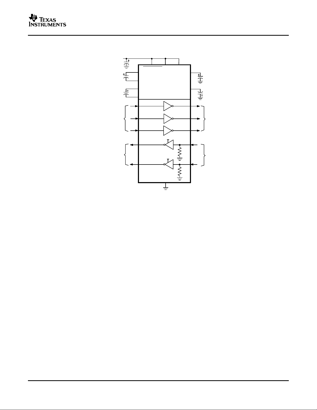
FUNCTIONAL BLOCK DIAGRAM
TERMINAL FUNCTIONS
TERMINAL
NAME NO.
C1+ 1 Positive terminal of the voltage-doubler charge-pump capacitor
V+ 2 5.5-V supply generated by the charge pump
C1– 3 Negative terminal of the voltage-doubler charge-pump capacitor
C2+ 4 Positive terminal of the inverting charge-pump capacitor
C2– 5 Negative terminal of the inverting charge-pump capacitor
V– 6 –5.5-V supply generated by the charge pump
DIN1 7
DIN2 8 Driver inputs
DIN3 9
ROUT2 10
ROUT1 11
V
L
RIN2 13
RIN1 14
DOUT3 15
DOUT2 16 RS-232 driver outputs
DOUT1 17
GND 18 Ground
V
CC
PWRDWN 20 L = Powerdown
Receiver outputs. Swing between 0 and VL.
12 Logic-level supply. All CMOS inputs and outputs are referenced to this supply.
RS-232 receiver inputs
19 3-V to 5.5-V supply voltage
Powerdown input
H = Normal operation
DESCRIPTION
Submit Documentation Feedback
2
www.ti.com
RS-232 TRANSCEIVER
WITH SPLIT SUPPLY PIN FOR LOGIC SIDE
SLLS659 – MAY 2006
MAX3386E
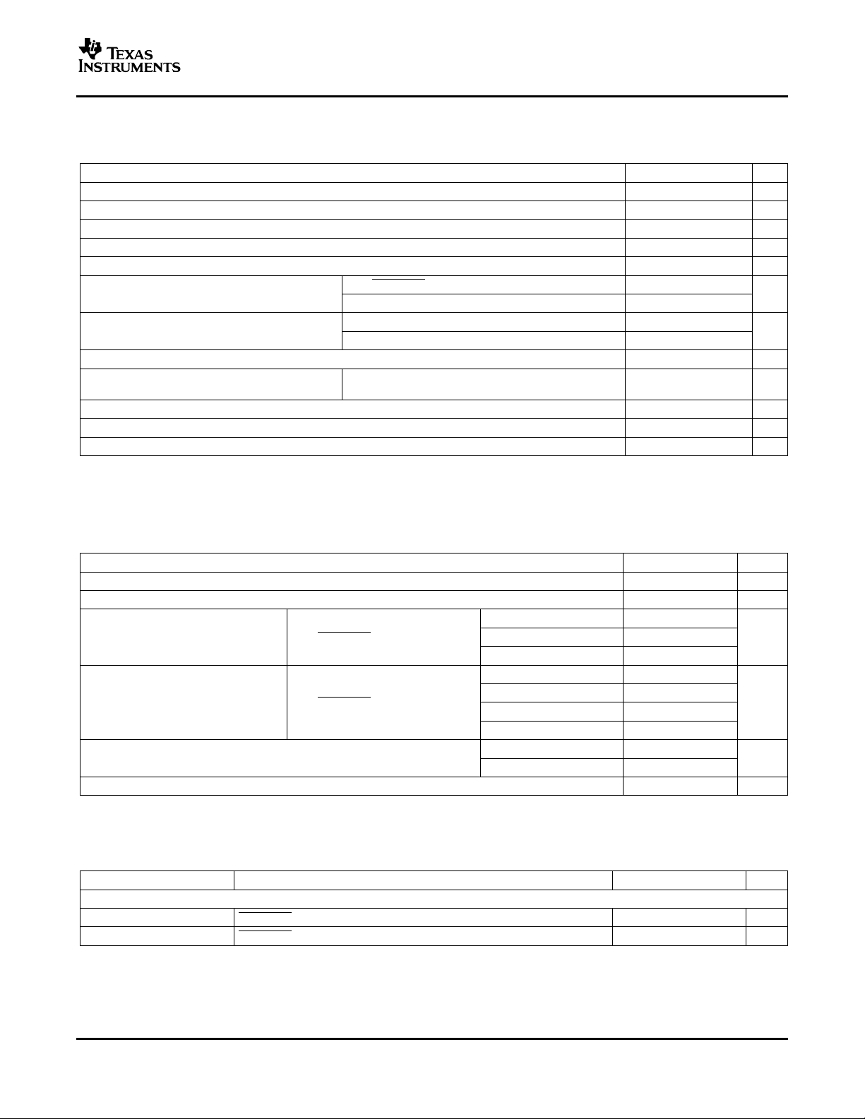
Absolute Maximum Ratings
(1)
over operating free-air temperature range (unless otherwise noted)
MIN MAX UNIT
V
to GND –0.3 6 V
CC
VLto GND –0.3 V
V+ to GND –0.3 7 V
V– to GND 0.3 – 7 V
V+ + |V–|
V
Input voltage V
I
V
Output voltage V
O
Short-circuit duration DOUT to GND Continuous
Continuous power dissipation 559 mW
T
Junction temperature 150 ° C
J
T
Storage temperature range –65 150 ° C
stg
Lead temperature (soldering, 10 s) 300 ° C
(1) Stresses beyond those listed under “absolute maximum ratings” may cause permanent damage to the device. These are stress ratings
only, and functional operation of the device at these or any other conditions beyond those indicated in the operational sections of the
specifications is not implied. Exposure to absolute maximum rating conditions for extended periods may affect device reliability.
(2) V+ and V– can have maximum magnitudes of 7 V, but their absolute difference cannot exceed 13 V.
(2)
DIN, PWRDWN to GND –0.3 6
RIN to GND ± 25
DOUT to GND ± 13.2
ROUT –0.3 VL+ 0.3
TA= 70 ° C, 20-pin TSSOP
(derate 7 mW/ ° C above 70 ° C)
CC
+ 0.3 V
13 V
Recommended Operating Conditions
MIN MAX UNIT
V
Supply voltage 3 5.5 V
CC
V
Supply voltage 1.65 V
L
CC
VL= 3 V or 5.5 V 0.8
Input logic threshold low DIN, PWRDWN VL= 2.3 V 0.6 V
VL= 1.65 V 0.5
VL= 5.5 V 2.4
Input logic threshold high DIN, PWRDWN V
VL= 3 V 2.0
VL= 2.7 V 1.4
VL= 1.95 V 0.9
Operating temperature ° C
MAX3386ECPWR 0 70
MAX3386EIPWR –40 85
Receiver input voltage –25 25 V
Electrical Characteristics
over operating free-air temperature range, V
C2–C4 = 0.33 µ F (tested at 5 V ± 10%) (unless otherwise noted)
PARAMETER TEST CONDITIONS MIN TYP
DC Characteristics (V
Powerdown supply current PWRDWN = GND, All inputs at V
Supply current PWRDWN = VCC, No load 0.3 1 mA
(1) Typical values are at V
= 3.3 V or 5 V, TA= 25 ° C)
CC
= VL= 3.3 V, TA= 25 ° C.
CC
= VL= 3 V to 5.5 V, C1–C4 = 0.1 µ F (tested at 3.3 V ± 10%), C1 = 0.047 µ F,
CC
(1)
or GND 1 10 µ A
CC
MAX UNIT
V
Submit Documentation Feedback
3
www.ti.com
MAX3386E
RS-232 TRANSCEIVER
WITH SPLIT SUPPLY PIN FOR LOGIC SIDE
SLLS659 – MAY 2006
ESD Protection
PARAMETER TEST CONDITIONS TYP UNIT
Human-Body Model ± 15
RIN, DOUT IEC 61000-4-2 Air-Gap Discharge ± 15 kV
IEC 61000-4-2 Contact Discharge ± 8
4
Submit Documentation Feedback
www.ti.com
RECEIVER SECTION
Electrical Characteristics
over operating free-air temperature range, V
C2–C4 = 0.33 µ F (tested at 5 V ± 10%), TA= T
PARAMETER TEST CONDITIONS MIN TYP
I
off
V
OL
V
OH
V
IT–
V
IT+
V
hys
(1) Typical values are at V
Output leakage current ROUT, receivers disabled ± 0.05 ± 10 µ A
Output voltage low I
Output voltage high I
OUT
OUT
Input threshold low TA= 25 ° C V
Input threshold high TA= 25 ° C V
Input hysteresis 0.5 V
Input resistance TA= 25 ° C 3 5 7 k Ω
= VL= 3.3 V, TA= 25 ° C
CC
Switching Characteristics
over operating free-air temperature range, V
C2–C4 = 0.33 µ F (tested at 5 V ± 10%), TA= T
PARAMETER TEST CONDITIONS TYP
t
PHL
t
PLH
t
– t
PHL
t
en
t
dis
Receiver propagation delay Receiver input to receiver output, CL= 150 pF µ s
Receiver skew 50 ns
PLH
Receiver output enable time From PWRDWN 200 ns
Receiver output disable time From PWRDWN 200 ns
MAX3386E
RS-232 TRANSCEIVER
WITH SPLIT SUPPLY PIN FOR LOGIC SIDE
SLLS659 – MAY 2006
= VL= 3 V to 5.5 V, C1–C4 = 0.1 µ F (tested at 3.3 V ± 10%), C1 = 0.047 µ F,
CC
to T
MIN
= 1.6 mA 0.4 V
= –1 mA VL– 0.6 VL– 0.1 V
= VL= 3 V to 5.5 V, C1–C4 = 0.1 µ F (tested at 3.3 V ± 10%), C1 = 0.047 µ F,
CC
to T
MIN
(unless otherwise noted)
MAX
(unless otherwise noted)
MAX
(1)
VL= 5 V 0.8 1.2
VL= 3.3 V 0.6 1.5
VL= 5 V 1.8 2.4
VL= 3.3 V 1.5 2.4
MAX UNIT
(1)
0.15
0.15
UNIT
(1) Typical values are at V
= VL= 3.3 V, TA= 25 ° C.
CC
Submit Documentation Feedback
5
www.ti.com
MAX3386E
RS-232 TRANSCEIVER
WITH SPLIT SUPPLY PIN FOR LOGIC SIDE
SLLS659 – MAY 2006
DRIVER SECTION
Electrical Characteristics
over operating free-air temperature range, V
C2–C4 = 0.33 µ F (tested at 5 V ± 10%), TA= T
PARAMETER TEST CONDITIONS MIN TYP
V
Output voltage swing All driver outputs loaded with 3 k Ω to ground ± 5 ± 5.4 V
OH
r
Output resistance V
o
I
Output short-circuit current V
OS
I
Output leakage current ± 25 µ A
OZ
Driver input hysteresis 0.5 V
Input leakage current DIN, PWRDWN ± 0.01 ± 1 µ A
(1) Typical values are at V
Timing Requirements
over operating free-air temperature range, V
C2–C4 = 0.33 µ F (tested at 5 V ± 10%), TA= T
PARAMETER MIN TYP
Maximum data rate RL= 3 k Ω , CL= 1000 pF, One driver switching 250 kbps
Time-to-exit powerdown |V
|t
– t
PLH
| Driver skew
Transition-region
slew rate
PHL
(1) Typical values are at V
(2) Driver skew is measured at the driver zero crosspoint.
= VL= 3.3 V, TA= 25 ° C
CC
(2)
= VL= 3.3 V, TA= 25 ° C.
CC
V
CC
TA= 25 ° C,
RL= 3 k Ω to 7 k Ω , V/ µ s
Measured from 3 V
to –3 V or –3 V to 3 V
= VL= 3 V to 5.5 V, C1–C4 = 0.1 µ F (tested at 3.3 V ± 10%), C1 = 0.047 µ F,
CC
to T
MIN
= V+ = V– = 0, Driver output = ± 2 V 300 10M Ω
CC
= 0 ± 60 mA
T_OUT
V
= ± 12 V, Driver disabled,
T_OUT
V
= 0 or 3 V to 5.5 V
CC
= VL= 3 V to 5.5 V, C1–C4 = 0.1 µ F (tested at 3.3 V ± 10%), C1 = 0.047 µ F,
CC
to T
MIN
| > 3.7 V 100 µ s
T_OUT
(unless otherwise noted)
MAX
(unless otherwise noted)
MAX
(1)
(1)
100 ns
= 3.3 V, CL= 150 pF to 1000 pF 6 30
CL= 150 pF to 2500 pF 4 30
MAX UNIT
MAX UNIT
ESD Protection
PARAMETER TEST CONDITIONS TYP UNIT
Human-Body Model ± 15
RIN, DOUT IEC 61000-4-2 Air-Gap Discharge ± 15 kV
IEC 61000-4-2 Contact Discharge ± 8
6
Submit Documentation Feedback
www.ti.com
ROUT210
ROUT111
RIN2
13
GND
18
TTL/CMOS
Inputs
DIN1
7
C2−
5
C2+
4
C1−
3
C1+
1
RIN1
14
DOUT2
16
DOUT1
17
V−
6
V+
2
V
CCVL
3.3 V
DOUT3
15
TTL/CMOS
Outputs
5kΩ
5kΩ
C3
0.1
µF
C4
0.1
µF
20 19 12
C1
0.1F
C2
0.1F
PWRDWN
DIN2
DIN3
C
BYPASS
V
L
V
L
MAX3386E
RS-232 TRANSCEIVER
WITH SPLIT SUPPLY PIN FOR LOGIC SIDE
SLLS659 – MAY 2006
APPLICATION INFORMATION
Submit Documentation Feedback
7
www.ti.com
50 Ω
TEST CIRCUIT
VOLTAGE WAVEFORMS
−3 V
−3 V
3 V
3 V
0 V
3 V
1.5 V1.5 V
Output
Input
V
OL
V
OH
t
TLH
Generator
(see Note B)
R
L
RS-232
Output
t
THL
C
L
(see Note A)
SR(tr)
6 V
t
THL
or t
TLH
3 V
PWRDWN
NOTES: A. CL includes probe and jig capacitance.
B. The pulse generator has the following characteristics: PRR = 250 kbit/s, ZO = 50 Ω, 50% duty cycle,
tr ≤ 10 ns, tf ≤ 10 ns.
50 Ω
TEST CIRCUIT VOLTAGE WAVEFORMS
0 V
3 V
Output
Input
V
OL
V
OH
t
PLH
Generator
(see Note B)
R
L
3 V
PWRDWN
RS-232
Output
t
PHL
C
L
(see Note A)
NOTES: A. CL includes probe and jig capacitance.
B. The pulse generator has the following characteristics: PRR = 250 kbit/s, ZO = 50 Ω, 50% duty cycle, tr ≤ 10 ns, tf ≤ 10 ns.
50%
50%
1.5 V
1.5 V
TEST CIRCUIT VOLTAGE WAVEFORMS
50 Ω
50%
50%
−3 V
3 V
1.5 V1.5 V
Output
Input
V
OL
V
OH
t
PHL
Generator
(see Note B)
t
PLH
Output
PWRDWN
3 V
C
L
(see Note A)
NOTES: A. CL includes probe and jig capacitance.
B. The pulse generator has the following characteristics: ZO = 50 Ω, 50% duty cycle, tr ≤ 10 ns, tf ≤ 10 ns.
MAX3386E
RS-232 TRANSCEIVER
WITH SPLIT SUPPLY PIN FOR LOGIC SIDE
SLLS659 – MAY 2006
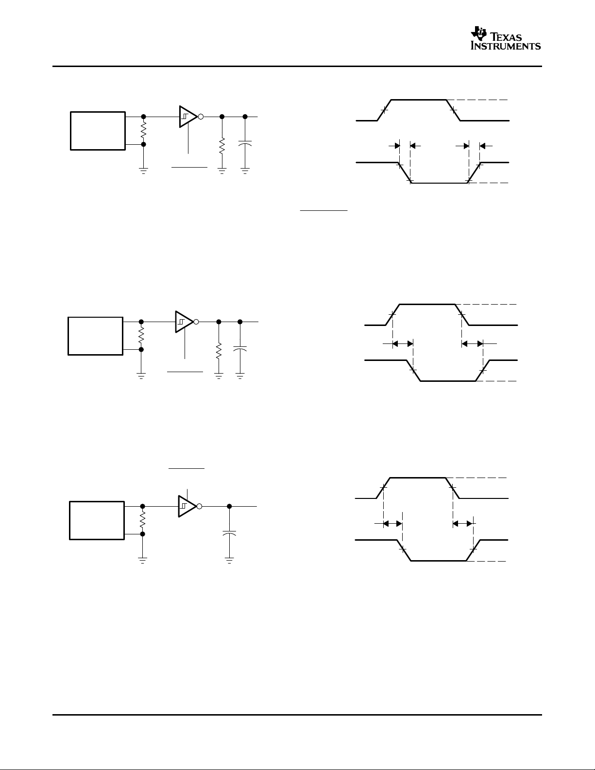
PARAMETER MEASUREMENT INFORMATION
Figure 1. Driver Slew Rate
8
Figure 2. Driver Pulse Skew
Figure 3. Receiver Propagation Delay Times
Submit Documentation Feedback

www.ti.com
PARAMETER MEASUREMENT INFORMATION
TEST CIRCUIT
VOLTAGE WAVEFORMS
50 Ω
Generator
(see Note B)
3 V or 0 V
Output
V
OL
V
OH
t
PZH
(S1 at GND)
t
PLZ
(S1 at VCC)
t
PHZ
S1 at GND)
t
PZL
(S1 at VCC)
1.5 V1.5 V
3 V
0 V
50%
0.3 V
Output
Input
50%
0.3 V
PWRDWN
R
L
S1
V
CC
GND
C
L
(see Note A)
Output
NOTES: A. CL includes probe and jig capacitance.
B. The pulse generator has the following characteristics: ZO = 50 Ω, 50% duty cycle, tr ≤ 10 ns, tf ≤ 10 ns.
MAX3386E
RS-232 TRANSCEIVER
WITH SPLIT SUPPLY PIN FOR LOGIC SIDE
SLLS659 – MAY 2006
Figure 4. Receiver Enable and Disable Times
Submit Documentation Feedback
9
PACKAGE OPTION ADDENDUM
www.ti.com
6-Dec-2006
PACKAGING INFORMATION
Orderable Device Status
(1)
Package
Type
Package
Drawing
Pins Package
Qty
Eco Plan
MAX3386ECDW ACTIVE SOIC DW 20 25 Green (RoHS &
no Sb/Br)
MAX3386ECDWG4 ACTIVE SOIC DW 20 25 Green (RoHS &
no Sb/Br)
MAX3386ECDWR ACTIVE SOIC DW 20 2000 Green (RoHS &
no Sb/Br)
MAX3386ECDWRG4 ACTIVE SOIC DW 20 2000 Green (RoHS&
no Sb/Br)
MAX3386ECPW ACTIVE TSSOP PW 20 70 Green (RoHS &
no Sb/Br)
MAX3386ECPWG4 ACTIVE TSSOP PW 20 70 Green (RoHS &
no Sb/Br)
MAX3386ECPWR ACTIVE TSSOP PW 20 2000 Green (RoHS &
no Sb/Br)
MAX3386ECPWRG4 ACTIVE TSSOP PW 20 2000 Green (RoHS &
no Sb/Br)
MAX3386EIDW ACTIVE SOIC DW 20 25 Green (RoHS &
no Sb/Br)
MAX3386EIDWG4 ACTIVE SOIC DW 20 25 Green (RoHS &
no Sb/Br)
MAX3386EIDWR ACTIVE SOIC DW 20 2000 Green (RoHS &
no Sb/Br)
MAX3386EIDWRG4 ACTIVE SOIC DW 20 2000 Green(RoHS &
no Sb/Br)
MAX3386EIPW ACTIVE TSSOP PW 20 70 Green (RoHS &
no Sb/Br)
MAX3386EIPWG4 ACTIVE TSSOP PW 20 70 Green (RoHS &
no Sb/Br)
MAX3386EIPWR ACTIVE TSSOP PW 20 2000 Green (RoHS &
no Sb/Br)
MAX3386EIPWRG4 ACTIVE TSSOP PW 20 2000 Green (RoHS &
no Sb/Br)
(1)
The marketing status values are defined as follows:
ACTIVE: Product device recommended for new designs.
LIFEBUY: TI has announced that the device will be discontinued, and a lifetime-buy period is in effect.
NRND: Not recommended for new designs. Device is in production to support existing customers, but TI does not recommend using this part in
a new design.
PREVIEW: Device has been announced but is not in production. Samples may or may not be available.
OBSOLETE: TI has discontinued the production of the device.
(2)
Lead/Ball Finish MSL Peak Temp
CU NIPDAU Level-1-260C-UNLIM
CU NIPDAU Level-1-260C-UNLIM
CU NIPDAU Level-1-260C-UNLIM
CU NIPDAU Level-1-260C-UNLIM
CU NIPDAU Level-1-260C-UNLIM
CU NIPDAU Level-1-260C-UNLIM
CU NIPDAU Level-1-260C-UNLIM
CU NIPDAU Level-1-260C-UNLIM
CU NIPDAU Level-1-260C-UNLIM
CU NIPDAU Level-1-260C-UNLIM
CU NIPDAU Level-1-260C-UNLIM
CU NIPDAU Level-1-260C-UNLIM
CU NIPDAU Level-1-260C-UNLIM
CU NIPDAU Level-1-260C-UNLIM
CU NIPDAU Level-1-260C-UNLIM
CU NIPDAU Level-1-260C-UNLIM
(3)
(2)
Eco Plan - The planned eco-friendly classification: Pb-Free (RoHS), Pb-Free (RoHS Exempt), or Green (RoHS & no Sb/Br) - please check
http://www.ti.com/productcontent for the latest availability information and additional product content details.
TBD: The Pb-Free/Green conversion plan has not been defined.
Pb-Free (RoHS): TI's terms "Lead-Free" or "Pb-Free" mean semiconductor products that are compatible with the current RoHS requirements
for all 6 substances, including the requirement that lead not exceed 0.1% by weight in homogeneous materials. Where designed to be soldered
at high temperatures, TI Pb-Free products are suitable for use in specified lead-free processes.
Pb-Free (RoHS Exempt): This component has a RoHS exemption for either 1) lead-based flip-chip solder bumps used between the die and
package, or 2) lead-based die adhesive used between the die and leadframe. The component is otherwise considered Pb-Free (RoHS
compatible) as defined above.
Green (RoHS & no Sb/Br): TI defines "Green" to mean Pb-Free (RoHS compatible), and free of Bromine (Br) and Antimony (Sb) based flame
retardants (Br or Sb do not exceed 0.1% by weight in homogeneous material)
Addendum-Page 1

PACKAGE OPTION ADDENDUM
www.ti.com
(3)
MSL, Peak Temp. -- The Moisture Sensitivity Level rating according to the JEDEC industry standard classifications, and peak solder
temperature.
Important Information and Disclaimer:The information provided on this page represents TI's knowledge and belief as of the date that it is
provided. TI bases its knowledge and belief on information provided by third parties, and makes no representation or warranty as to the
accuracy of such information. Efforts are underway to better integrate information from third parties. TI has taken and continues to take
reasonable steps to provide representative and accurate information but may not have conducted destructive testing or chemical analysis on
incoming materials and chemicals. TI and TI suppliers consider certain information to be proprietary, and thus CAS numbers and other limited
information may not be available for release.
In no event shall TI's liability arising out of such information exceed the total purchase price of the TI part(s) at issue in this document sold by TI
to Customer on an annual basis.
6-Dec-2006
Addendum-Page 2


MECHANICAL DATA
MTSS001C – JANUARY 1995 – REVISED FEBRUARY 1999
PW (R-PDSO-G**) PLASTIC SMALL-OUTLINE PACKAGE
14 PINS SHOWN
0,65
1,20 MAX
14
0,30
0,19
8
4,50
4,30
PINS **
7
Seating Plane
0,15
0,05
8
1
A
DIM
14
0,10
6,60
6,20
M
0,10
0,15 NOM
0°–8°
2016
Gage Plane
24
0,25
0,75
0,50
28
A MAX
A MIN
NOTES: A. All linear dimensions are in millimeters.
B. This drawing is subject to change without notice.
C. Body dimensions do not include mold flash or protrusion not to exceed 0,15.
D. Falls within JEDEC MO-153
3,10
2,90
5,10
4,90
5,10
4,90
6,60
6,40
7,90
7,70
9,80
9,60
4040064/F 01/97
POST OFFICE BOX 655303 • DALLAS, TEXAS 75265

IMPORTANT NOTICE
Texas Instruments Incorporated and its subsidiaries (TI) reserve the right to make corrections, modifications,
enhancements, improvements, and other changes to its products and services at any time and to discontinue
any product or service without notice. Customers should obtain the latest relevant information before placing
orders and should verify that such information is current and complete. All products are sold subject to TI’s terms
and conditions of sale supplied at the time of order acknowledgment.
TI warrants performance of its hardware products to the specifications applicable at the time of sale in
accordance with TI’s standard warranty. Testing and other quality control techniques are used to the extent TI
deems necessary to support this warranty . Except where mandated by government requirements, testing of all
parameters of each product is not necessarily performed.
TI assumes no liability for applications assistance or customer product design. Customers are responsible for
their products and applications using TI components. To minimize the risks associated with customer products
and applications, customers should provide adequate design and operating safeguards.
TI does not warrant or represent that any license, either express or implied, is granted under any TI patent right,
copyright, mask work right, or other TI intellectual property right relating to any combination, machine, or process
in which TI products or services are used. Information published by TI regarding third-party products or services
does not constitute a license from TI to use such products or services or a warranty or endorsement thereof.
Use of such information may require a license from a third party under the patents or other intellectual property
of the third party, or a license from TI under the patents or other intellectual property of TI.
Reproduction of information in TI data books or data sheets is permissible only if reproduction is without
alteration and is accompanied by all associated warranties, conditions, limitations, and notices. Reproduction
of this information with alteration is an unfair and deceptive business practice. TI is not responsible or liable for
such altered documentation.
Resale of TI products or services with statements different from or beyond the parameters stated by TI for that
product or service voids all express and any implied warranties for the associated TI product or service and
is an unfair and deceptive business practice. TI is not responsible or liable for any such statements.
Following are URLs where you can obtain information on other Texas Instruments products and application
solutions:
Products Applications
Amplifiers amplifier.ti.com Audio www.ti.com/audio
Data Converters dataconverter.ti.com Automotive www.ti.com/automotive
DSP dsp.ti.com Broadband www.ti.com/broadband
Interface interface.ti.com Digital Control www.ti.com/digitalcontrol
Logic logic.ti.com Military www.ti.com/military
Power Mgmt power.ti.com Optical Networking www.ti.com/opticalnetwork
Microcontrollers microcontroller.ti.com Security www.ti.com/security
Low Power Wireless www.ti.com/lpw Telephony www.ti.com/telephony
Video & Imaging www.ti.com/video
Wireless www.ti.com/wireless
Mailing Address: Texas Instruments
Post Office Box 655303 Dallas, Texas 75265
Copyright 2006, Texas Instruments Incorporated
 Loading...