

Page 1
LP55XX
CALIBRATION
MEMORY
SPI/I2C
INTER-
FACE
BOOSTADC
COLOR AND
BRIGHTNESS
PWM LOGIC
LED
DRIVERS
MCU
WITH
I2C
OR
SPI
-+
C
OUT
C
VDDA
C
VDDD
100 nF 4.7 PF
C
IN
2.9 ± 5.5V 5 ± 20V
FB
SW
100 nF
2 x
4.7 PF
4.7 PH
L1
ROUT
LP5520
V
DDA
V
DDD
S1_IN
S2_IN
PWMR
PWMG
PWMB
V
LDO
NRST
SS/SDA
SCK/SCL
SI/A0
SO
IFSEL
C
VDDIO
100 nF
V
DDIO
C
VLDO
1 PF
BRC
GND
LM 20
V
LDO
GOUT
BOUT
D1
Product
Folder
Sample &
Buy
Technical
Documents
Tools &
Software
Support &
Community
SNVS440B –MAY 2007–REVISED MARCH 2016
LP5520 RGB Backlight LED Driver
LP5520
1 Features
1
• Temperature Compensated LED Intensity and
Color
• Individual Calibration Coefficients for Each Color
• Color Accuracy ΔX and ΔY ≤ 0.003
• 12-Bit ADC for Measurement of 2 Sensors
• Adjustable Current Outputs for Red, Green, and
Blue (RGB) LED
• 0.2% Typical LED Output Current Matching
• PWM Control Inputs for Each Color
• SPI™ and I2C-Compatible Interface
• Stand-Alone Mode With One-Wire Control
• Sequential Mode for One Color at a Time
• Magnetic High Efficiency Boost Converter
• Programmable Output Voltage from 5 V to 20 V
• Adaptive Output Voltage Control Option
• < 2-µA Typical Shutdown Current
2 Applications
• Color LCD Display Backlighting
• LED Lighting Applications
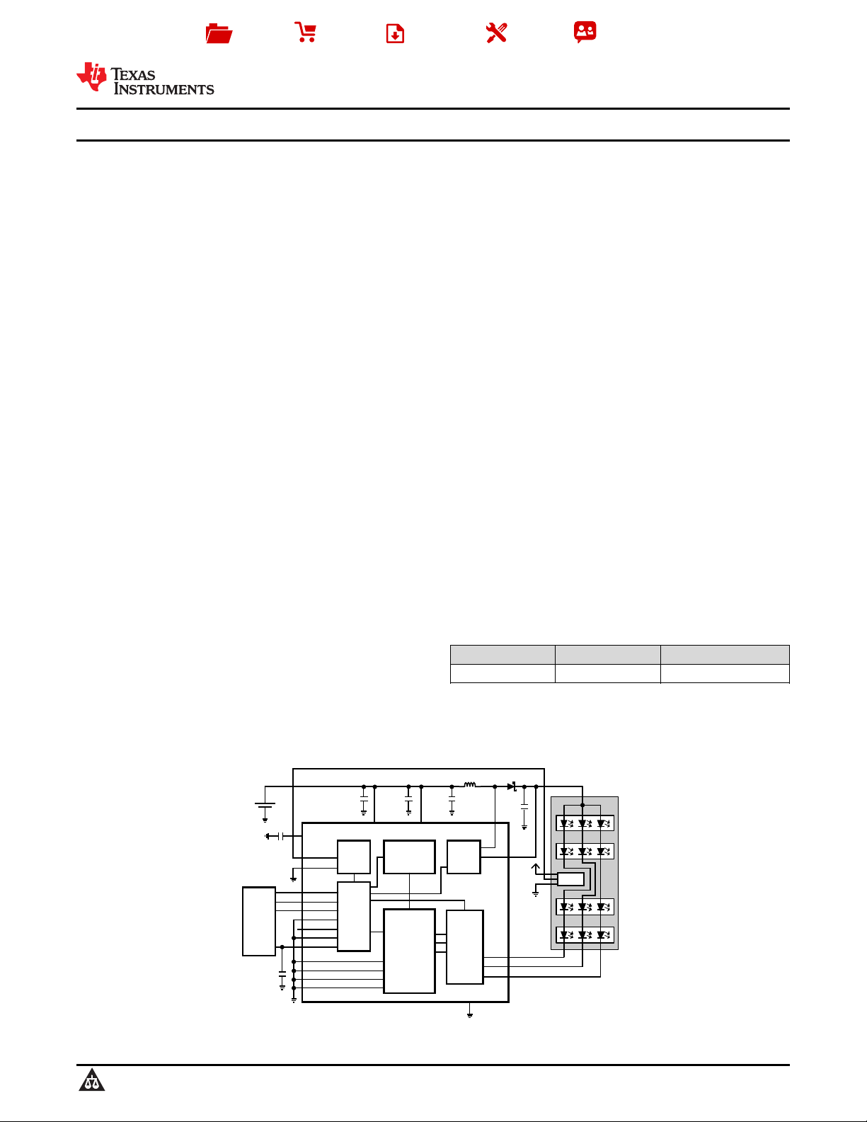
3 Description
The LP5520 is an RGB backlight LED driver for small
format color LCDs. RGB backlights enable better
colors on the display and power savings compared
with white LED backlights. The device offers a small
and simple driver solution without need for optical
feedback. Calibration in display module production
can be done in one temperature. The LP5520
produces true white light over a wide temperature
range. Three independent LED drivers have accurate
programmable current sinks and PWM modulation
control. Using internal calibration memory and
external temperature sensor, the RGB LED currents
are adjusted for perfect white balance independent of
the brightness setting or temperature. The user
programmable calibration memory has intensity vs
temperature data for each color. This white balance
calibration data can be programmed to the memory
on the production line of a backlight module.
The device has a magnetic boost converter that
creates a supply voltage of up to 20 V LED from the
battery voltage. The output can be set at 1-V steps
from 5 V to 20 V. In adaptive mode the circuit
automatically adjusts the output voltage to minimum
sufficient level for lowest power consumption.
Temperature is measured using an external
temperature sensor placed close to the LEDs. The
second ADC input can be used, for example, for
ambient light measurement.
1
An IMPORTANT NOTICE at the end of this data sheet addresses availability, warranty, changes, use in safety-critical applications,
intellectual property matters and other important disclaimers. PRODUCTION DATA.
PART NUMBER PACKAGE BODY SIZE (MAX)
LP5520 DSBGA (25) 2.787 mm × 2.621 mm
(1) For all available packages, see the orderable addendum at
the end of the data sheet.
Typical Application
Device Information
(1)
Page 2

LP5520
SNVS440B –MAY 2007–REVISED MARCH 2016
www.ti.com
Table of Contents
1 Features.................................................................. 1
2 Applications ........................................................... 1
3 Description ............................................................. 1
4 Revision History..................................................... 2
5 Pin Configuration and Function........................... 3
6 Specifications......................................................... 4
6.1 Absolute Maximum Ratings ...................................... 4
6.2 ESD Ratings.............................................................. 4
6.3 Recommended Operating Conditions....................... 4
6.4 Thermal Information.................................................. 4
6.5 Electrical Characteristics........................................... 5
6.6 RGB Driver Electrical Characteristics (ROUT, GOUT,
BOUT Outputs) .......................................................... 5
6.7 Logic Interface Characteristics.................................. 6
6.8 Magnetic Boost DC-DC Converter Electrical
Characteristics ........................................................... 6
6.9 I2C Timing Parameters ............................................. 7
6.10 SPI Timing Requirements ....................................... 7
6.11 Typical Characteristics............................................ 8
7 Detailed Description.............................................. 9
7.1 Overview ................................................................... 9
7.2 Functional Block Diagram......................................... 9
7.3 Feature Description................................................... 9
7.4 Device Functional Modes........................................ 18
7.5 Programming........................................................... 22
7.6 Register Maps......................................................... 28
8 Application and Implementation ........................ 33
8.1 Application Information............................................ 33
8.2 Typical Applications ............................................... 33
9 Power Supply Recommendations...................... 37
10 Layout................................................................... 37
10.1 Layout Guidelines ................................................. 37
10.2 Layout Example .................................................... 38
11 Device and Documentation Support ................. 39
11.1 Device Support...................................................... 39
11.2 Documentation Support ........................................ 39
11.3 Community Resources.......................................... 39
11.4 Trademarks........................................................... 39
11.5 Electrostatic Discharge Caution............................ 39
11.6 Glossary................................................................ 39
12 Mechanical, Packaging, and Orderable
Information........................................................... 40
4 Revision History
NOTE: Page numbers for previous revisions may differ from page numbers in the current version.
Changes from Revision A (May 2013) to Revision B Page
• Changed "R, G and B" to "Red, Green, and Blue"................................................................................................................. 1
• Deleted "Non-Linear Temperature Compensation" and "Ambient Light Compensation" from Applications ......................... 1
• Added Device Information and Pin Configuration and Functions sections, ESD Ratings and Thermal Information
tables, Feature Description, Device Functional Modes, Application and Implementation, Power Supply
Recommendations, Layout, Device and Documentation Support, and Mechanical, Packaging, and Orderable
Information sections................................................................................................................................................................ 1
• Changed "MAIN, SUB" to " ROUT, GOUT, BOUT"................................................................................................................ 4
• Changed "come" to "are loaded".......................................................................................................................................... 12
• Changed ", and also the variable" to ". The variable parameter"......................................................................................... 18
• Changed "makes possible" to "allows" ................................................................................................................................. 19
• Changed "read" to "loaded".................................................................................................................................................. 19
• Changed "The stand-alone mode must be inhibited in automatic and manual modes by writing the control bit
<brc_off> high and by keeping BRC input low." to new text .............................................................................................. 19
Changes from Original (April 2013) to Revision A Page
• Changed layout of National Data Sheet to TI format ........................................................................................................... 32
2
Submit Documentation Feedback Copyright © 2007–2016, Texas Instruments Incorporated
Product Folder Links: LP5520
Page 3
GNDT
1
2
3
4
5
A
B
C
D
E
SW FB
GND
_SW
GOUT BOUT
ROUT S2_IN
GND
_LED
S1_IN
BRC
VDDA
VDDD SO
SS/
SDA
GNDA
PWMR IFSEL
PWMG VDDIO
VLDO
NRST
PWMB
SI/
A0
SCK/
SCL
GNDT
1
2
3
4
5
A
B
C
D
E
SWFB
GND
_SW
GOUTBOUT
ROUTS2_IN
GND
_LED
S1_IN
BRC
VDDA
VDDD
SI/
A0
SO
SCK/
SCL
GNDA
PWMRIFSEL
PWMGVDDIO
VLDO
NRST
PWMB
SS/
SDA
www.ti.com
5 Pin Configuration and Function
LP5520
SNVS440B –MAY 2007–REVISED MARCH 2016
YZR Packge
25-Pin DSBGA
Top View
YZR Packge
25-Pin DSBGA
Bottom View
Pin Functions
PIN
NUMBER NAME
1A VDDA Power Supply voltage for analog circuitry
1B GNDT Ground Ground/Test
1C S1_IN Input ADC input 1, input for temperature sensor
1D BOUT Output Blue LED output
1E GOUT Output Green LED output
2A VLDO Power Internal LDO output
2B BRC Logic Input Brightness control for all LED outputs
2C S2_IN Input ADC input 2, input for optional second sensor
2D PWMB Logic Input PWM control for output B
2E ROUT Output Red LED output
3A VDDIO Power Supply voltage for input/output buffers and drivers
3B NRST Logic Input Master reset, active low
3C PWMG Logic Input PWM control for output G
3D GNDA Ground Ground for analog circuitry
3E GND_LED Ground Ground for LED currents
4A SS/SDA Logic Input/Output Slave select (SPI), serial data in/out (I2C)
4B SCK/SCL Logic Input Clock (SPI/I2C)
4C IFSEL Logic Input Interface selection (SPI or I2C-compatible, IF_SEL = 1 for SPI)
4D PWMR Logic Input PWM control for output R
4E GND_SW Ground Power switch ground
5A SO Logic Output Serial data out (SPI)
5B SI/A0 Logic Input Serial input (SPI), address select (I2C)
5C VDDD Power Supply voltage for digital circuitry
5D FB Input Boost converter feedback
5E SW Output Boost converter power switch
TYPE DESCRIPTION
Submit Documentation FeedbackCopyright © 2007–2016, Texas Instruments Incorporated
Product Folder Links: LP5520
3
Page 4
LP5520
SNVS440B –MAY 2007–REVISED MARCH 2016
www.ti.com
6 Specifications
6.1 Absolute Maximum Ratings
over operating free-air temperature range (unless otherwise noted)
V (SW, FB, ROUT, GOUT, BOUT) –0.3 22 V
V
, V
, V
DDA
DDD
DDIO
, V
LDO
Voltage on logic pins –0.3 V to V
Continuous power dissipation
Junction temperature, T
Storage temperature, T
(4)
J-MAX
stg
(1) Stresses beyond those listed under Absolute Maximum Ratings may cause permanent damage to the device. These are stress ratings
only, which do not imply functional operation of the device at these or any other conditions beyond those indicated under Recommended
Operating Conditions. Exposure to absolute-maximum-rated conditions for extended periods may affect device reliability.
(2) All voltages are with respect to the potential at the GND pins.
(3) If Military/Aerospace specified devices are required, contact the TI Sales Office/Distributors for availability and specifications.
(4) Internal thermal shutdown circuitry protects the device from permanent damage. Thermal shutdown engages at TJ= 160°C (typical) and
disengages at TJ= 140°C (typical).
6.2 ESD Ratings
V
(ESD)
Electrostatic discharge
(1) JEDEC document JEP155 states that 500-V HBM allows safe manufacturing with a standard ESD control process.
(2) JEDEC document JEP157 states that 250-V CDM allows safe manufacturing with a standard ESD control process.
Human-body model (HBM), per ANSI/ESDA/JEDEC JS-001
Charged-device model (CDM), per JEDEC specification JESD22-C101
(1)(2)(3)
MIN MAX UNIT
–0.3 6 V
DDIO
0.3 V with 6 V
maximum
V
Internally limited
125 °C
–65 150 °C
VALUE UNIT
(1)
(2)
±2000
±200
V
6.3 Recommended Operating Conditions
over operating free-air temperature range (unless otherwise noted)
V (SW, FB, ROUT, GOUT, BOUT) 0 21 V
V
DDA,DDD
V
DDIO
Recommended load current (ROUT, GOUT, BOUT) per driver 0 60 mA
Junction temperature, T
Ambient temperature, T
(1) All voltages are with respect to the potential at the GND pins.
(2) In applications where high power dissipation and/or poor package thermal resistance is present, the maximum ambient temperature may
have to be derated. Maximum ambient temperature (T
125°C), the maximum power dissipation of the device in the application (P
part/package in the application (R
J
(2)
A
) is dependent on the maximum operating junction temperature (T
A-MAX
), as given by the following equation: T
θJA
(1)
MIN MAX UNIT
2.9 5.5 V
1.65 V
DDA
V
–30 125 °C
–30 85 °C
), and the junction-to ambient thermal resistance of the
D-MAX
A-MAX
= T
J-MAX-OP
– (R
θJA
× P
D-MAX
).
J-MAX-OP
=
6.4 Thermal Information
LP5520
THERMAL METRIC
R
θJA
R
θJC(top)
R
θJB
ψ
JT
ψ
JB
Junction-to-ambient thermal resistance 58.2 °C/W
Junction-to-case (top) thermal resistance 0.3 °C/W
Junction-to-board thermal resistance 7.9 °C/W
Junction-to-top characterization parameter 0.5 °C/W
Junction-to-board characterization parameter 7.9 °C/W
(1) For more information about traditional and new thermal metrics, see the Semiconductor and IC Package Thermal Metrics application
report, SPRA953.
(1)
UNITYZR (DSBGA)
25 PINS
4
Submit Documentation Feedback Copyright © 2007–2016, Texas Instruments Incorporated
Product Folder Links: LP5520
Page 5
LP5520
www.ti.com
SNVS440B –MAY 2007–REVISED MARCH 2016
6.5 Electrical Characteristics
Unless otherwise noted typical limits are for TJ= 25°C, minimum and maximum limits apply over the operating ambient
temperature range (–30°C < TJ< +85°C), and specifications apply to the LP5520 Functional Block Diagram with: C
100 nF, C
= 2 × 4.7 µF, 25 V, CIN= 10 µF, 6.3 V, L1 = 4.7 µH.
OUT
(1)(2)(3)
PARAMETER TEST CONDITIONS MIN TYP MAX UNIT
I
VDD
I
VDDIO
V
LDO
I
LDO
Standby supply current
(V
+ V
DDD
)
DDA
No-boost supply current
(V
+ V
DDD
)
DDA
No-load supply current
(V
+ V
)
DDD
standby supply current NSTBY = L 1 µA
V
DDA
DDIO
NSTBY = L, V
NSTBY = L , V
NSTBY = H,
EN_BOOST = L
NSTBY = H, EN_BOOST = H
AUTOLOAD = L
Internal LDO output voltage VIN≥ 2.9 V, TJ= 25°C 2.77 2.80 2.84 V
Internal LDO output current Current to external load 1 mA
≥ 1.65 V 1.7 7
DDIO
= 0 V 1
DDIO
0.9
1.4
(1) All voltages are with respect to the potential at the GND pins.
(2) Minimum and maximum limits are specified by design, test or statistical analysis. Typical numbers represent the most likely norm.
(3) Low-ESR Surface-Mount Ceramic Capacitors (MLCCs) used in setting electrical characteristics.
VDDA/D
6.6 RGB Driver Electrical Characteristics (ROUT, GOUT, BOUT Outputs)
Typical limits are for TJ= 25°C, minimum and maximum limits apply over the operating ambient temperature range
(–30°C < TJ< +85°C); over operating free-air temperature range (unless otherwise noted).
PARAMETER TEST CONDITIONS MIN TYP MAX UNIT
I
LEAKAGE
I
MAX
I
R
I
MATCH
t
PWM
ƒ
RGB
V
SAT
ƒ
MAX
(1) Matching is the maximum difference from the average when all outputs are set to same current.
(2) Saturation voltage is defined as the voltage when the LED current has dropped 10% from the value measured at 2 V.
ROUT, GOUT, BOUT pin
leakage current
Maximum sink current
Current accuracy of ROUT,
GOUT, and BOUT
Matching
(1)
Outputs ROUT, GOUT, BOUT control = 255
(FFH)
Output current set to 20 mA
Output current set to 60 mA
19 20 21 mA
–5% 5%
54 60 66 mA
–10% 10%
Between ROUT, GOUT, BOUT at 20 mA current ±0.2% ±2%
0.1 1 µA
60
PWM cycle time Accuracy proportional to internal clock frequency 820 µs
RGB switching frequency
Saturation voltage
(2)
External PWM maximum
frequency
<pwm_fast> = 0 1.22 kHz
<pwm_fast> = 1 19.52
I
= 60 mA 550 mV
(LED)
I
= 60 mA, TJ= 25°C 1 MHz
(LED)
=
µA
mA
mA
Product Folder Links: LP5520
Submit Documentation FeedbackCopyright © 2007–2016, Texas Instruments Incorporated
5
Page 6
LP5520
SNVS440B –MAY 2007–REVISED MARCH 2016
6.7 Logic Interface Characteristics
Typical limits are for TJ= 25°C, minimum and maximum limits apply over the operating ambient temperature range
(–30°C < TJ< +85°C); over operating free-air temperature range (unless otherwise noted).
PARAMETER TEST CONDITIONS MIN TYP MAX UNIT
LOGIC INPUTS SS, SI/A0, SCK/SCL, IFSEL, NRST, PWMR, PWMG, PWMB and BRC
V
IL
V
IH
I
I
ƒ
SCK/SLC
LOGIC INPUT NRST
V
IL
V
IH
I
I
t
NRST
LOGIC OUTPUT SO
V
OL
V
OH
I
L
LOGIC OUTPUT SDA
V
OL
Input low level 0.2 × V
Input high level 0.8 × V
DDIO
DDIO
Logic input current −1 1 µA
I2C mode 0.4
Clock frequency
SPI mode, V
SPI mode, 1.65 V < V
1.8 V
> 1.8 V 13
DDIO
<
DDIO
Input low level 05 V
Input high level 1.2 V
Logic input current –1 1 µA
Reset pulse width 10 µs
Output low level
Output high level
ISO= 3 mA
V
> 1.8 V
DDIO
ISO= 2 mA
1.65 V < V
ISO= –3 mA
V
> 1.8 V
DDIO
ISO= –2 mA
1.65 V < V
DDIO
DDIO
< 1.8 V
< 1.8 V
V
V
DDIO
DDIO
− 0.5 V
− 0.5 V
0.3 0.5 V
0.3 0.5 V
− 0.3 V
DDIO
− 0.3 V
DDIO
Output leakage current VSO= 2.8 V 1 µA
Output low level I
= 3 mA 0.3 0.5 V
SDA
www.ti.com
V
V
MHz
5
6.8 Magnetic Boost DC-DC Converter Electrical Characteristics
Typical limits are for TJ= 25°C, minimum and maximum limits apply over the operating ambient temperature range
(–30°C < TJ< +85°C); over operating free-air temperature range (unless otherwise noted).
PARAMETER TEST CONDITIONS MIN TYP MAX UNIT
I
LOAD
V
OUT
RDS
ƒ
PWM
t
PULSE
t
STARTUP
I
MAX
6
Maximum continuous load
current
Output voltage accuracy (FB pin)
ON
Switch ON resistance ISW= 0.5 A 0.3 Ω
Frequency accuracy
Switch pulse minimum width no load 50 ns
Start-up time 20 ms
SW pin current limit 1100 mA
Submit Documentation Feedback Copyright © 2007–2016, Texas Instruments Incorporated
2.9V = VIN, V
TJ= 25°C
2.9 ≤ VIN≤ 5.5 V, V
TJ= 25°C
2.9 ≤ VIN≤ 5.5 V, V
OUT
= 20 V
= 20 V
OUT
= 20 V –5% 5%
OUT
70
–1.7% 1.7%
TJ= 25°C −6% ±3% 6%
–9% 9%
Product Folder Links: LP5520
mA
Page 7
SCK
Data
BIT 1 LSB IN
LSB OUTBIT 1
MSB OUT
BIT 7BIT 8BIT 9BIT 14MSB IN
R/WAddress
2 1
4
5
7
6
3
11
9
10
8
SS
SO
SI
12
SDA
SCL
1
8
2
3
7
6
5
8
10
4 9
1 7
www.ti.com
SNVS440B –MAY 2007–REVISED MARCH 2016
6.9 I2C Timing Parameters
V
= 3 V to 4.5 V, V
DD1,2
= 1.8 V To V
DDIO
; see Figure 1.
DD1,2
MIN MAX UNIT
1 Hold time (repeated) START condition 0.6 µs
2 Clock low time 1.3 µs
3 Clock high time 600 ns
4 Setup time for a repeated START condition 600 ns
5 Data hold time (output direction, delay generated by LP5520) 300 900 ns
5 Data hold time (input direction, delay generated by Master) 0 900 ns
6 Data setup time 100 ns
7 Rise time of SDA and SCL 20 + 0.1C
8 Fall time of SDA and SCL 15 + 0.1C
b
b
300 ns
300 ns
9 Setup time for STOP condition 600 ns
10 Bus free time between a STOP and a START condition 1.3 µs
C
b
Capacitive load for each bus line 10 200 pF
6.10 SPI Timing Requirements
See Figure 2.
MIN MAX UNIT
1 Cycle time 70 ns
2 Enable lead time 35 ns
3 Enable lag time 35 ns
4 Clock low time 35 ns
5 Clock high time 35 ns
6 Data setup time 0 ns
7 Data hold time 25 ns
8 Data access time 30 ns
9 Disable time 20 ns
10 Data valid 40 ns
11 Data hold time 0 ns
LP5520
Figure 1. I2C Timing Diagram
Figure 2. SPI Timing Diagram
Product Folder Links: LP5520
Submit Documentation FeedbackCopyright © 2007–2016, Texas Instruments Incorporated
7
Page 8
AUTOLOAD OFF
AUTOLOAD ON
20.017.014.011.08.05.0
OUTPUT VOLTAGE (V)
INPUT CURRENT (mA)
1.0
2.0
3.0
4.0
5.0
6.0
7.0
8.0
0.0 0.5 1.0 1.5 2.0 2.5 3.0 3.5 4.0
TIME (s)
8.0
7.0
6.0
5.0
4.0
3.0
2.0
1.0
0.0
V
BOOST
V
LOAD
V
DRIVER
VOLTAGE (V)
8.0
7.0
6.0
5.0
4.0
3.0
2.0
1.0
0.0
0 60 120 180 240 300 360
OUTPUT CURRENT (mA)
20.0
18.0
16.0
14.0
12.0
10.0
8.0
6.0
4.0
VIN= 2.9V
VIN= 3.6V
INDUCTOR TDK VLF3010 - 4.7 mH
OUTPUT VOLTAGE (V)
V
OUT
= 20V
V
OUT
=1 5V
V
OUT
= 10V
INDUCTOR TDK VLF3010 - 4.7 PH
I
LOAD
= 60 mA
600
600
500
450
400
350
300
250
200
150
BATTERY CURRENT (mA)
BATTERY VOLTAGE (V)
2.9 3.1 3.3 3.5 3.7 3.9 4.1
OUTPUT CURRENT (mA)
OUTPUT VOLTAGE (V)
0.0 0.2 0.4 0.6 0.8 1.0
0.0
10.0
20.0
30.0
40.0
50.0
60.0
OUTPUT CURRENT (mA)
OUTPUT VOLTAGE (V)
0.0 0.2 0.4 0.6 0.8 1.0
0.0
10.0
20.0
30.0
40.0
50.0
60.0
LP5520
SNVS440B –MAY 2007–REVISED MARCH 2016
6.11 Typical Characteristics
6.11.1 RGB Driver Typical Characteristics
www.ti.com
Figure 3. V
SAT
vs I
LED
6.11.2 Boost Converter Typical Characteristics
VIN= 3.6 V, V
Figure 5. Boost Maximum Output Voltage vs Current
= 15 V, if not otherwise stated.
OUT
Figure 4. V
SAT
vs I
LED
Figure 6. Battery Current vs Voltage
8
Figure 7. Auto-Load Effect on Input Current, No Load Figure 8. Adaptive Output Voltage Operation
Submit Documentation Feedback Copyright © 2007–2016, Texas Instruments Incorporated
Product Folder Links: LP5520
Page 9
CALIBRATION
EEPROM
SPI/I2C
INTER-
FACE
AND
CONTROL
BOOST
ADC
COLOR
PWM
LOGIC
LED
DRIVERS
CURRENT
DACS
ANALOG
SUPPORT
TEMP
SENSOR
LM20
MCU or
TESTER
with SPI
interface
-+
C
OUT
C
VDDD
C
VDDA
100 nF
4.7 PF
C
IN
2.9 V± 5.5V
5 V ± 20V
FB
SW
100 nF
2 x
4.7 PF
4.7 PH
L1
ROUT
S1_IN
S2_IN
PWMR
PWMG
PWMB
V
DDIO
RST
SS/SDA
SCK/SCL
SI/A0
SO
IFSEL
GND_A GND_LED GND_SW
C
VDDIO
100 nF
V
DDD
V
DDA
C
VLDO
1 PF
LP5520
V
LDO
0 ± 60 mA
0 ± 60 mA
0 ± 60 mA
BRC
Optional EMI
filter
close to SW pin
Optional
Ferrite
Bead
D1
GND_T
C
SW
R
SW
3.9 :
330 pF
Optional HF
capacitor
C
HF
68 pF
GOUT
BOUT
L
SW
LP5520
www.ti.com
SNVS440B –MAY 2007–REVISED MARCH 2016
7 Detailed Description
7.1 Overview
The LP5520 is an RGB backlight LED driver for small format color LCDs. The LP5520 offers a small and simple
driver solution without need for optical feedback. Calibration in display module production can be done in one
temperature. The LP5520 produces true white light over a wide temperature range.
Three independent LED drivers have accurate programmable current sinks with up to 60 mA current capability
and PWM modulation control. Using internal calibration memory and external temperature sensor, the RGB LED
currents are adjusted for perfect white balance independent of the brightness setting or temperature. The user
programmable calibration memory has intensity vs temperature data for each color. This white balance
calibration data can be programmed to the memory on the production line of a backlight module.
The LP5520 has a magnetic boost converter that creates supply voltage up to 20-V LED from the battery
voltage. The output can be set at 1-V step from 5 V to 20 V. In adaptive mode the circuit automatically adjusts
the output voltage to minimum sufficient level for lowest power consumption.
Temperature is measured using an external temperature sensor placed close to the LEDs. The second ADC
input can be used, for example, for ambient light measurement.
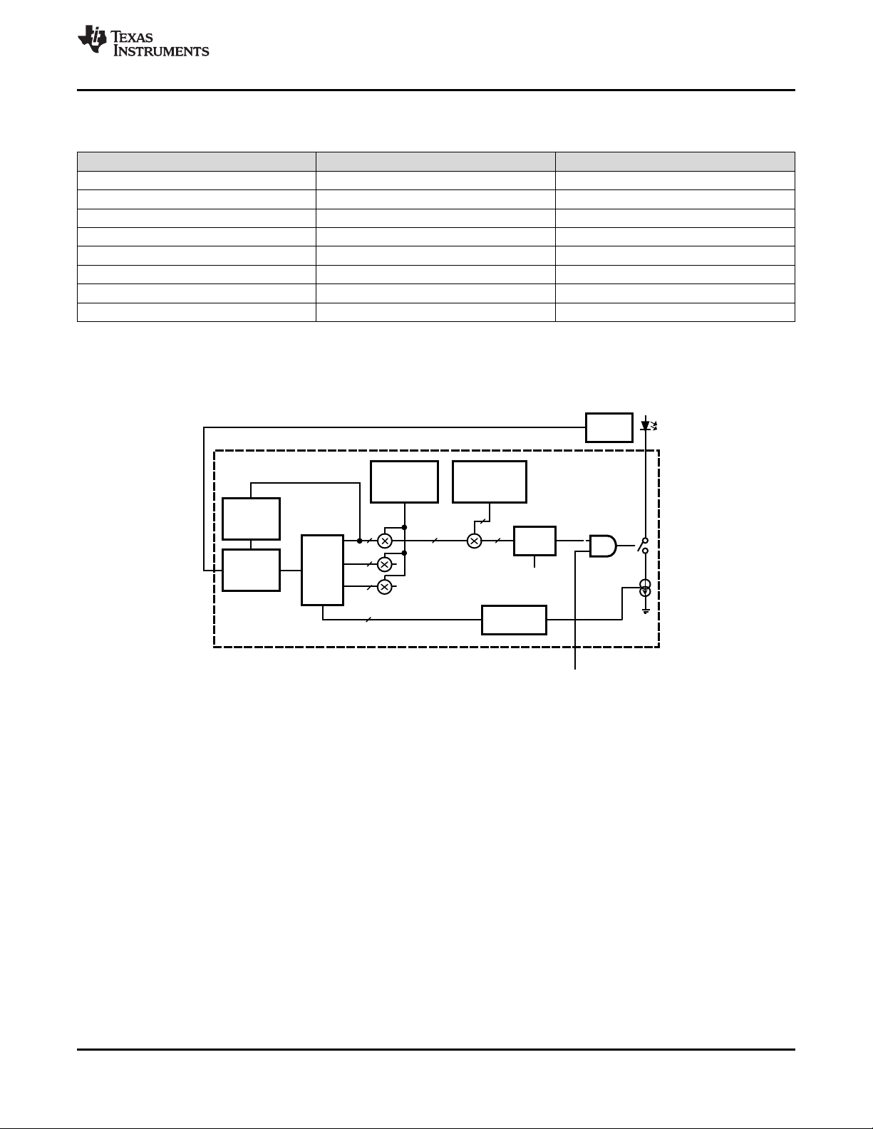
7.2 Functional Block Diagram
and V
must be tied together and turned on first. V
DDA
7.3 Feature Description
7.3.1 Start-Up Powering
V
DDD
later. In the power-off sequence V
must be turned off before V
DDIO
DDIO
must be turned on at the same time as V
DDD
Product Folder Links: LP5520
or at the same time.
Submit Documentation FeedbackCopyright © 2007–2016, Texas Instruments Incorporated
DDD
or
9
Page 10
-40 -20 0 20 40 60 80
TEMPERATURE
4000
3500
3000
2500
2000
1500
1000
500
0
Red
Blue
Green
INTENSITY
4000
3500
2500
2000
3000
1500
1000
500
0
0
0.1
0.2
0.3
0.4
0.5
0.6
0.7
0.8
0.9
700
620
600
580
560
540
520
500
480
470
Target for white
light
X
Y
Green
Blue
Red
460
490
380
0 0.1 0.3 0.4 0.5 0.6 0.7 0.80.2
V
DDIO
Power ON Power OFF
V
DDD
and V
DDA
LP5520
SNVS440B –MAY 2007–REVISED MARCH 2016
www.ti.com
Feature Description (continued)
Figure 9. Power-On Signal Timing
7.3.2 RGB Driver Functionality
7.3.2.1 White Balance Control
The LP5520 is designed to provide spectrally rich white light using a three-color RGB LED. White light is
obtained when the red, green, and blue LED intensities are in proper balance. The LED intensities change
independently with temperature. For maintaining the purity of the white color and the targeted total intensity,
precise temperature dependent intensity control for each LED is required. The color coordinates in this document
refer to the CIE 1931 color graph (x,y system).
Figure 11 shows a typical RGB LED intensity behavior on a 12-bit scale (0 to 4095) at constant 20-mA LED
currents. Figure 12 shows the typical color coordinate change for an uncompensated RGB LED. Figure 13 shows
the corresponding PWM values for achieving constant intensity white light across the temperature range. The
PWM values have been saturated at 104°C to avoid overheating the LED and to better utilize the PWM range.
The white balance is not maintained above 104°C in this case.
10
Submit Documentation Feedback Copyright © 2007–2016, Texas Instruments Incorporated
Figure 10. CIE 1931 Color Graph
Figure 11. LED Intensity vs Temperature
Product Folder Links: LP5520
Page 11
-40 -20 0 20 40 60 80
TEMPERATURE, °C
0.310
0.305
0.300
0.295
0.290
Y
X
COLOR COORDINATES
0.310
0.305
0.300
0.295
0.290
-40 -20 0 20 40 60 80 100 120
TEMPERATURE
4000
3500
3000
2500
2000
1500
1000
500
0
Red
Blue
Green
PWM VALUE
4000
3500
3000
2500
2000
1500
1000
500
0
-40 -14 12 38 64 90
TEMPERATURE,°C
0.34
0.32
0.31
0.29
0.28
0.26
X
Y
COLOR COORDINATE
0.34
0.32
0.31
0.29
0.28
0.26
LP5520
www.ti.com
SNVS440B –MAY 2007–REVISED MARCH 2016
Feature Description (continued)
Figure 12. Typical Color Coordinates vs Temperature for Uncompensated RGB LED
The compensation values for the measured temperatures can be easily calculated when the intensity vs
temperature information is available. For the best accuracy the iterative calibration approach must be used.
The compensation values must be converted to 16°C intervals when they are programmed to the calibration
EEPROM. The evaluation software has import function, which can be used to convert the measured
compensation data to the 16°C interval format. The measured data can have any temperature points, and the
software fits a curve through the measured points and calculate new PWM values in fixed temperatures using the
curves.
Typical color coordinate and intensity stability over temperature are shown in Figure 14 and Figure 15.
Figure 13. Compensation PWM Values
Figure 14. Compensated Color Coordinates vs Temperature
Submit Documentation FeedbackCopyright © 2007–2016, Texas Instruments Incorporated
Product Folder Links: LP5520
11
Page 12
-40 -20 0 20 40 60 80
TEMPERATURE, °C
1500
1450
1400
1350
1300
INTENSITY BLUE
1500
1450
1400
1350
1300
LP5520
SNVS440B –MAY 2007–REVISED MARCH 2016
www.ti.com
Feature Description (continued)
Figure 15. Compensated Blue LED Intensity vs Temperature
7.3.2.2 LED Brightness Control
The LED brightness is defined by two factors, the current through the LED and the PWM duty cycle. The
constant current outputs ROUT, GOUT, and BOUT can be independently set to sink between 0 and 60 mA. The
8-bit current control has 255 levels, and the step size is 235 µA. In manual mode the current is defined with the
current control (R/G/B) registers (01H, 02H, and 03H). In automatic mode the current settings are loaded from
the EEPROM.
The PWM control has 12-bit resolution, which means 4095 steps. The minimum pulse width is 200 ns, and the
frequency can be set to either 1.2 kHz or 19.2 kHz. The duty cycle range is from 0 to 100% (0 to 4095). The
output PWM value is obtained by multiplication of three factors. The first factor is the temperature-based value
from the EEPROM. The second factor is the correction register setting, which is independent for each color. The
third factor is the brightness register setting, which is common to all colors.
The temperature-based PWM values are stored in the EEPROM at 16°C intervals starting from –40°C and
ending to 120°C. PWM values for the temperatures between the stored points are interpolated.
LED brightness has 3-bit logarithmic control. The control bits are in the pwm_brightness (04H) register. The 3-bit
value defines a multiplier for the 12-bit PWM value obtained from the memory according to Table 1.
12
Submit Documentation Feedback Copyright © 2007–2016, Texas Instruments Incorporated
Product Folder Links: LP5520
Page 13
SELF
HEATING
COMPENS.
EEPROM
+
LOGIC
ADC
+
LOGIC
BRIGHTNESS
0.8 ± 100%
8 STEP LOG
CORRECTION R
0 ± 200%
(AGEING COMP)
CURRENT R
0 ± 60mA
TEMP
SENSOR
PWM
GEN
R
G
B
S1_IN
PWM_R
12 1212
12
12
5 MHz
8
8
ROUT
LP5520
www.ti.com
SNVS440B –MAY 2007–REVISED MARCH 2016
Feature Description (continued)
Table 1. PWM Value Multipliers
CONTROL BYTE <bri[2:0]>
0 0.008 0.8
1 0.016 1.6
2 0.031 3.1
3 0.063 6.3
4 0.125 12.5
5 0.250 25
6 0.500 50
7 1.000 100
(1) PWM Brightness register control
The brightness correction can be used for aging compensation or other fine-tuning. There is an 8-bit correction
register for each output. The PWM value obtained from the memory is multiplied by the correction value. The
default correction value is 1. Correction range is from 0 to 2 and the LSB is 0.78% (1/128).
(1)
MULTIPLIER INTENSITY ( %)
Shown complete only for red channel
Figure 16. LED Control Principle
7.3.2.3 LED PWM Control
The PWM frequency can be selected of two alternatives, slow and fast, with the control bit <pwm_fast>. The
slow frequency is 1.2 kHz. In the fast mode the PWM frequency is multiplied by 16, and the frequency is 19.2
kHz. Fast mode is the default mode after reset. The single pulse in normal PWM is split in 16 narrow pulses in
fast PWM. Higher frequency helps eliminate possible noise from the ceramic capacitors and it also reduces the
ripple in the boost voltage. Minimum pulse length is 200 ns in both modes.
The PWM pulses of each output do not start simultaneously in order to avoid high current spike. Red starts in the
beginning of the PWM cycle, Green is symmetric with the cycle center and Blue ends in the end of the cycle. For
PWM values less than 33% for each output, the output currents are completely non-overlapping. With higher
PWM values the overlapping increases.
Product Folder Links: LP5520
Submit Documentation FeedbackCopyright © 2007–2016, Texas Instruments Incorporated
13
Page 14
ROUT
GOUT
BOUT
PWMR
PWMG
PWMB
10 ms/100 Hz
3.333 ms
3.333 ms
3.333 ms
Dead time
1
2
3
4
Internal PWM cycle
1 2 3
4
1 2
3
4
ROUT
GOUT
BOUT
0%
50%
100%
819 Ps/1.22 kHz in normal PWM
52 Ps/19.2 kHz in fast PWM
LP5520
SNVS440B –MAY 2007–REVISED MARCH 2016
www.ti.com
Figure 17. Pulse Positions in the PWM Cycle
7.3.2.4 Sequential Mode
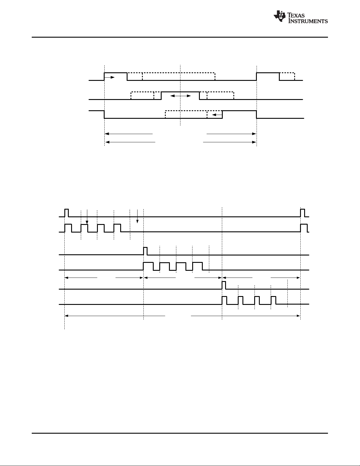
Completely non-overlapping timing can be obtained by using the sequential mode as shown in Figure 18. The
timing is defined with external PWM control inputs. The minimum trigger pulse width in the PWM inputs is 1 µs.
There is no limitation on the maximum width of the pulse as long as it is shorter than the whole sequence.
Figure 18. Non-Overlapping External Synchronized Sequential Mode
In sequential mode the PWM cycle is synchronized to trigger pulses and the amount of PWM pulses per trigger
can be defined to 2, 3 or 4 using the <seq_mode0> and <seq_mode1> control bits. This makes possible to use
sequence lengths of about 5 ms, 7.5 ms or 10 ms. Fast PWM can be used in sequential mode, but the frame
timing is as with normal PWM.
The PWM timing and synchronization timing originate from different clock sources. Some margin must be
allowed for clock tolerances. This margin shows as a dead time in the waveform graph. Some dead time must be
allowed so that no PWM pulse is clipped. Clipping would distort the intensity balance between the LEDs. The
dead time causes some intensity reduction, but assures the current balance.
PWM mode is defined by <seq_mode1> and <seq_mode2> control bits of rgb_control (00H) register:
14
Submit Documentation Feedback Copyright © 2007–2016, Texas Instruments Incorporated
Product Folder Links: LP5520
Page 15

LP5520
www.ti.com
SNVS440B –MAY 2007–REVISED MARCH 2016
Table 2. PWM Mode
<seq_mode1>
(BIT 7)
0 0 Normal mode
0 1 Sequential mode with 2 PWM pulses per trigger
1 0 Sequential mode with 3 PWM pulses per trigger
1 1 Sequential mode with 4 PWM pulses per trigger
<seq_mode0>
(BIT 6)
MODE
7.3.2.5 Current Control of the LEDs
The LP5520 has a separate 8-bit current control for each LED output. In manual mode the current for red LED is
controlled with the current_control_r (01H) register, the green LED is controlled with the current_control_g
(02H), and the blue LED with current_control_b (03H). Output current can be calculated with formula: current
(mA) = code × 0.235; for example, a 20-mA current is obtained with code 85 (55H).
In automatic and stand-alone modes the LED current values programmed in EEPROM are used, and the current
control registers have no effect. There are two ways to change the default current if needed. The defaults can be
changed permanently by programming new values to the EEPROM. The other option is to make a temporary
change by writing new current values in SRAM.
7.3.2.6 Output Enables
ROUT, GOUT, and BOUT output activity is controlled with 3 enable bits of the rgb_control (00H) register:
Table 3. Output Enable Bits
<en_b> (bit 2) 0 Blue LED output BOUT disabled
1 Blue LED output BOUT enabled
<en_g> (bit 1) 0 Green LED output GOUT disabled
1 Green LED output GOUT enabled
<en_r> (bit 0) 0 Red LED output ROUT disabled
1 Red LED output ROUT enabled
PWM control inputs PWMR, PWMG and PWMB can be used as external output enables in normal and automatic
mode. In the sequential mode these inputs are the trigger inputs for respective outputs.
7.3.2.7 Fade In and Fade Out
The LP5520 has an automatic fade in and out for the LED outputs. Fading makes the transitions smooth in on
and off switching or when brightness is changed. It is not applied for the changes caused by the compensation
algorithm. The fade can be turned on and off using the <en_fade> bit in the rgb_control (00H) register. The
fade time is constant 520 ms, and it does not depend on how big the brightness change is. The white balance is
maintained during fading. Fading is off in the stand-alone mode.
Table 4. Fade In and Fade Out With <en_fade> Bit
<en_fade>(bit 5)
0 Automatic fade disabled
1 Automatic fade enabled
Product Folder Links: LP5520
Submit Documentation FeedbackCopyright © 2007–2016, Texas Instruments Incorporated
15
Page 16

2:1
MUX
AVERAGE
S1_RESULT
S2_RESULT
1:2
MUX
S1_IN
S2_IN
12 BIT ADC
LP5520
SNVS440B –MAY 2007–REVISED MARCH 2016
www.ti.com
Fading only works in automatic mode. The LED current registers must be written to 0 for proper fade operation.
When the LEDs are turned on with fading, it is best to set the brightness first and then enable the outputs and
automatic mode. The LEDs can be turned off then by turning off the automatic mode (write rgb_auto to 0).
7.3.2.8 Temperature and Light Measurement
The LP5520 has a 12-bit analog-to-digital converter (ADC) for the measurements. The ADC has two inputs.
S1_IN input is intended for the LM20 temperature sensor and S2_IN input for light measurement or any DC
voltage measurement. The conversion results are filtered with average filter for 134 ms. The <adc_ch> bit in the
Control register selects, which conversion result can be read out from the registers ADC_hi_byte and
ADC_low_byte. The ADC_hi_byte must be read first. The <comp_ch> bit selects, which input is used for
compensation. The ADC uses the LDO voltage 2.8 V as the reference voltage. The input signal range is 0 V to
2.8 V, and the inputs are buffered on the chip.
If S2_IN is used for light measurement using TDK optical sensor BCS2015G1 as shown in the Functional Block
Diagram, the measurement range is from 10 to 20 000 lux when using a 100-kΩ resistor.
Table 5. ADC Configuration
adc_ch(bit5) 0 S1 input can be read
1 S2 input can be read
comp_sel(bit4) 0 S1 input is used for compensation
1 S2 input is used for compensation
Figure 19. ADC Operation Block Diagram
7.3.3 Magnetic High-Voltage Boost DC-DC Converter
The LP5520 boost DC-DC converter generates a 5-V to 20-V supply voltage for the LEDs from single Li-Ion
battery (2.9 V to 4.5V). The output voltage is controlled with four bits in 18 steps. In adaptive mode the output
voltage is automatically adjusted so that the LED drivers have enough voltage for proper operation. The
converter is a magnetic switching PWM mode DC-DC converter with a current limit. Switching frequency is 1
MHz. Boost converter options are controlled with few bits of Control (06H) register.
Table 6. Boost DC-DC Converter Control
<en_autoload> (bit 3) 0 Internal boost converter loader off
1 Internal boost converter loader on
<vout_auto> (bit 2) 0 Manual boost output adjustment
1 Adaptive boost output adjustment
<en_boost> (bit 1) 0 Boost converter standby mode
1 Boost converter active mode
<nstby> (bit 0) 0 LP5520 standby mode
1 LP5520 active mode
The LP5520 boost converter uses pulse-skipping elimination to stabilize the noise spectrum. Even with light load
or no load a minimum length current pulse is fed to the inductor. An active load is used to remove the excess
charge from the output capacitor at very light loads. Active load can be disabled with the <en_autoload> bit.
Disabling active load increases slightly the efficiency at light loads, but the downside is that pulse skipping
occurs. The boost converter must be stopped when there is no load to minimize the current consumption.
The topology of the magnetic boost converter is called current programmed mode (CPM) control, where the
inductor current is measured and controlled with the feedback. The user can program the output voltage of the
boost converter. The output voltage control changes the resistor divider in the feedback loop.
16
Submit Documentation Feedback Copyright © 2007–2016, Texas Instruments Incorporated
Product Folder Links: LP5520
Page 17

+
-
+
+
-
+
-
FB
SW
R
S
R
R
R
Duty control1 MHz clock
OVPCOMP
ERRORAMP
SLOPER
OLPCOMP
RESETCOMP
LOOPC
+
-
ACTIVE
LOAD
SWITCH
+
-
UVCOMP
2V
+
-
R
I
MAX
OCPCOMP
R
V
IN
V
OUT
LP5520
www.ti.com
SNVS440B –MAY 2007–REVISED MARCH 2016
Figure 20 shows the boost topology with the protection circuitry. Four different protection schemes are
implemented:
1. Overvoltage protection: limits the maximum output voltage and:
– Keeps the output below breakdown voltage.
– Prevents boost operation if battery voltage is much higher than desired output.
2. Overcurrent protection: limits the maximum inductor current and:
– Voltage over switching NMOS is monitored; voltages too high turn off the switch.
3. Feedback break protection: prevents uncontrolled operation if FB pin is disconnected.
4. Duty cycle limiting done with digital control.
Figure 20. Boost Converter Topology
7.3.3.1 Boost Control
User can set the boost converter to standby mode by writing the register bit <en_boost> low. When <en_boost>
is written high, the converter starts for 50 ms in low current PWM mode and then goes to normal PWM mode.
User can control the boost output voltage by boost output boost_output (05H) register.
Table 7. Boost Output Voltage Control
BOOST OUTPUT [7:0]
REGISTER 0DH
Bin Dec
00101 5 5 V
00110 6 6 V
00111 7 7 V
... ... ...
01100 12 12 V
01101 13 13 V
01110 14 14 V
... ... ...
10010 18 18 V
10011 19 19 V
10100 20 20 V
Product Folder Links: LP5520
Submit Documentation FeedbackCopyright © 2007–2016, Texas Instruments Incorporated
BOOST OUTPUT
VOLTAGE (TYPICAL)
17
Page 18

LP5520
SNVS440B –MAY 2007–REVISED MARCH 2016
www.ti.com
If register value is lower than 5, then value of 5 is used internally. If register value is higher than 20, then value of
20 is used internally.
7.3.3.2 Adaptive Output Voltage Control
When automatic boost voltage control is selected using the <vout_auto> bit in the Control (06H) register, the
user-defined boost output voltage is ignored. The boost output voltage is adjusted for sufficient operating
headroom by monitoring all enabled LED driver outputs. The boosted voltage is adjusted so that the lowest driver
voltage is from 0.85 V to 1.35 V when the LED output currents are below 30 mA and from 1 V to 1.5V when any
LED current is above 30 mA. The output voltage range is from 5 V to 20 V in adaptive mode.
The adaptive voltage control helps saving energy by always setting the boost voltage to minimum sufficient
value. It eliminates the need for extra voltage margins due to LED forward voltage variation or temperature
variation. With very small brightness settings, when the PWM pulses in LED outputs are very narrow, the
adaptive voltage setting gives higher than necessary boost voltage. This does not harm the overall efficiency,
because this happens only at low power levels.
After reset the adaptive control is on by default. In stand-alone mode the adaptive output voltage is always used.
7.4 Device Functional Modes
The LP5520 has three different operating modes: manual mode, automatic mode, and stand-alone mode.
Automatic mode has two sub modes: normal mode and sequential mode. In manual and automatic modes the
device is controlled through the serial interface. In stand-alone mode only BRC input must be controlled, and all
registers have the default values. The modes are controlled according Table 8.
Table 8. Device Operating Modes Control
<RGB_auto>
(RBG control bit 3)
0 00 Manual mode
1 00 Automatic mode, normal operation (overlapping)
1 01, 10, or 11 Automatic mode, sequential operation with 2, 3, or 4 pulses per sequence
<seq_mode[0:1]>
(RBG control bits 6 and 7)
DEVICE OPERATING MODE
7.4.1 Manual Mode
In the manual mode the automatic LED intensity adjustment is not in use. The internal PWM control is disabled,
and the LEDs are driven with DC current. The user can set the LED currents through the serial port using three
current control registers, current_control_R/G/B, and use the external PWM control inputs to adjust LED
intensities if needed. There is an independent PWM control pin for each output. If PWM control is not used, the
PWMR, PWMG, and PWMR inputs must be tied to the V
. All the functions implemented with the internal
DDIO
PWM control are unavailable in manual mode (logarithmic brightness control from PWM Control register,
temperature compensation, fading, sequential mode).
7.4.2 Automatic Mode
In the automatic mode the LED intensities are controlled with the 12-bit PWM values obtained from the EEPROM
memory according to the temperature information. PWM values are stored at 16°C intervals for the
–40°C to +120°C temperature range, and the PWM values for the intermediate temperatures are linearly
interpolated.
When creating white light from a RGB LED, the intention is to program PWM values, which keep the individual
LED intensities constant in all temperatures. For possible other applications, other kind of PWM behavior can be
programmed. The variable parameter can be other than temperature if the sensor is changed to, for example, a
light sensor.
12-bit ADC is used for the measurements. The ADC has two inputs: S1_IN and S2_IN. The temperature
measurement result from the S1_IN input is converted to EEPROM address using the sensor calibration data
from EEPROM. This EEPROM address is then used to get the PWM values for each output. The second input
S2_IN can be used for example for ambient light measurement. The ADC data from selected input can be read
through the serial interface. Control bit <comp_sel> can be used to select which input is used for compensation.
18
Submit Documentation Feedback Copyright © 2007–2016, Texas Instruments Incorporated
Product Folder Links: LP5520
Page 19

LP5520
www.ti.com
SNVS440B –MAY 2007–REVISED MARCH 2016
Current setting for each LED comes from EEPROM in the automatic mode. The same current values must be
programmed as were used in the calibration. Current control range is from 0 to 60 mA with 8-bit resolution and
the step size is 235 µA.
Common brightness control for all LEDs can be done using the pwm_brightness (05H) register. The
pwm_brightness register makes 8 level logarithmic brightness control with 3 bits. An automatic fade function
allows smooth turnon, turnoff, and brightness changes of the LEDs. White balance is maintained during fading.
A brightness correction value can be given for each LED. The PWM value obtained from the EEPROM memory
is multiplied by this correction value. This feature can be used for example for LED aging compensation or for
color adjustment by user. These values are kept in R_correction (0AH), G_correction (0BH) and B_correction
(0CH) registers. The correction multiplier can be between 0 and 2.
Due to LED self-heating, the temperature sensor and the LED temperatures will differ. The difference depends
on the thermal structure of the display module and the distance between the sensor and the LEDs. This
temperature difference can be compensated by storing the temperature difference value at highest power (100%
red LED PWM) in the EEPROM memory. The system then corrects the measured temperature based on the
actual PWM value used. The correction assumes that the red LED PWM value is representing the whole RGB
LED power consumption.
Sequential (non-overlapping) drive is possible using external PWM control inputs to trigger a new sequence in
each LED output. 60 mA maximum current setting makes possible 20 mA maximum averaged current for each
output in the non-overlapping mode.
7.4.3 Stand-Alone Mode
In stand-alone mode the operation is controlled through a single PWM brightness input, BRC. After power-up or
reset the LP5520 is ready for stand-alone operation without any setup through the serial interface. The standalone mode is entered with a rising edge in the BRC input. The boost converter operates in adaptive mode. The
LED current settings are loaded from EEPROM. The LED brightness is controlled with a PWM signal in the BRC
input. The BRC PWM frequency must be from 2 to 10 kHz. The PWM signal in the BRC input is not used as
such for the LED outputs, but it is converted to 3-bit value and a logarithmic brightness control is based on this 3bit value, as shown in Table 9. There is hysteresis in the conversion to avoid blinking when the BRC duty cycle is
close to a threshold. When the PWM pulses end in the BRC input and the input stays low, the circuit goes to the
standby mode.
Figure 21 shows the waveforms in BRC input and ROUT output in the stand-alone mode. The circuit is in
standby mode until the first rising edge in BRC input is detected. The circuit starts up, and the outputs activate
after 30 ms from the first rising edge in BRC. The BRC frequency is assumed to 2 kHz in this example giving 0.5
ms BRC period. When the duty cycle changes in BRC, it takes two BRC periods before the change is reflected in
the output. When BRC goes permanently low, the circuit enters standby mode after 15 ms from the last BRC
pulse.
All controls through the serial interface can be used in the stand-alone mode. In Automatic and Manual mode the
control bit <brc_off> must be written high and BRC input kept low to prevent the LP5520 device from entering
stand-alone mode.
Table 9. Stand-Alone Mode Brightness Control
BRC DUTY CYCLE THRESHOLD VALUES (%) INTENSITY
(% of maximum)
INCREASING DECREASING INCREASING DECREASING
0 off 0
1 15 0.8 10 10
20 28 1.6 28 22
35 42 3.1 40 32
48 52 6.3 53 47
58 62 12.5 63 58
68 75 25 75 70
82 90 50 88 85
97 100 99
Product Folder Links: LP5520
RECOMMENDED BRC PWM CONTROL VALUES
Submit Documentation FeedbackCopyright © 2007–2016, Texas Instruments Incorporated
19
Page 20

CALIBRATION
EEPROM
SPI / I2C
INTER-
FACE
AND
CONTROL
BOOST
ADC
COLOR
PWM
LOGIC
LED
DRIVERS
CURRENT
DACS
ANALOG
SUPPORT
TEMP
SENSOR
LM20
-+
C
OUT
C
VDDA
C
VDDD
100 nF
4.7 PF
C
IN
2.9 ± 5.5V
5 ± 20V
FB
SW
100 nF
10 PF
4.7 PH
L1
S1_IN
S2_IN
PWMR
PWMG
PWMB
V
DDIO
NRST
SS/SDA
SCK/SCL
SI/A0
SO
IFSEL
GND_A GND_LED GND_SW
V
DDD
V
DDA
C
VLDO
1 PF
LP5520
V
LDO
20 mA
BRC
GND_T
ROUT
GOUT
BOUT
PWM INPUT
ON/OFF/
BRIGHTNESS
20 mA
20 mA
C
VDDIO
100 nF
ADAPTIVE
BRC
ROUT
Turn on delay
Turn off
delay
15 ms
PWM
cycle
Change
delay
2 periods
BRC
period
50 Ps
200 Ps
30 ms
LP5520
SNVS440B –MAY 2007–REVISED MARCH 2016
Figure 21. LP5520 Control and Output Waveforms in Stand-Alone Mode
www.ti.com
20
Figure 22. LP5520 Connections in Stand-Alone Mode
Submit Documentation Feedback Copyright © 2007–2016, Texas Instruments Incorporated
Product Folder Links: LP5520
Page 21

RESET
STANDBY
INTERNAL
STARTUP SEQUENCE
~20 ms DELAY
BOOST STARTUP
NORMAL MODE
NRST = L
or
POR = H
1) TSD = L
NRST = H
and
NSTBY = H or BRC = H
EN_BOOST = H
1
NSTBY = L and NRST = H
EEPROM AND EEPROM
READING (~1 ms)
V
REF
= 95% OK
1
~10 ms DELAY
NSTBY = L or BRC = L
and
NRST = H
TSD = H
EN_BOOST
RISING EDGE
1
EN_BOOST = L
1
LP5520
www.ti.com
SNVS440B –MAY 2007–REVISED MARCH 2016
7.4.4 Start-Up Sequence RESET: In the RESET mode all the internal registers are reset to the default values, and the chip goes to
STANDBY mode after reset. <NSTBY> control bit is low after reset by default. Reset is entered
always if NRST input is low or internal power on reset (POR) is active. POR activates during the
chip start-up or when the supply voltage VDD falls below 1.5 V. Once VDD rises above 1.5 V, POR
inactivates, and the device continues to the STANDBY mode.
STANDBY: The STANDBY mode is entered if the register bit <NSTBY> is LOW. This is the low-power
consumption mode, when all circuit functions are disabled. Registers can be written in this mode,
and the control bits are effective immediately after power up.
STARTUP: When <NSTBY> bit is written high or there is a rising edge in the BRC input, the INTERNAL
STARTUP SEQUENCE powers up all the needed internal blocks (Vref, Bias, Oscillator, etc.). To
ensure the correct initialization, a 10-ms delay is generated by the internal state-machine after the
trim EEPROM values are read. If the chip temperature rises too high, the thermal shutdown (TSD)
disables the chip operation, and STARTUP mode is entered until no TSD event is present.
BOOST STARTUP: Soft start for boost output is generated in the BOOST STARTUP mode. The boost output is
raised in PWM mode during the 20-ms delay generated by the state machine. All LED outputs are
off during the 20-ms delay to ensure smooth start-up. The boost start-up is entered from internal
start-up sequence if <EN_BOOST> is HIGH or from Normal mode when <EN_BOOST> is written
HIGH.
NORMAL: During NORMAL mode the user controls the chip using the control registers or the BRC input in
stand-alone mode. The registers can be written in any sequence and any number of bits can be
altered in a register in one write.
Figure 23. Device Functional Modes
Submit Documentation FeedbackCopyright © 2007–2016, Texas Instruments Incorporated
Product Folder Links: LP5520
21
Page 22

SDA
SCL
S
P
START condition
STOP condition
SCL
SDA
data
change
allowed
data
valid
data
change
allowed
data
valid
data
change
allowed
LP5520
SNVS440B –MAY 2007–REVISED MARCH 2016
www.ti.com
7.5 Programming
7.5.1 Control Interface
The LP5520 supports two different interface modes:
• SPI interface (4-wire, serial), and
• I2C-compatible interface (2-wire, serial)
User can define the serial interface by IF_SEL pin. IF_SEL = 0 selects the I2C mode.
7.5.1.1 I2C Compatible Interface
7.5.1.1.1 I2C Signals
The serial interface is in I2C mode when IF_SEL = 0. The SCL pin is used for the I2C clock and the SDA pin is
used for bidirectional data transfer. Both these signals need a pullup resistor according to I2C specification. The
values of the pullup resistors are determined by the capacitance of the bus (typical resistance is 1.8 kΩ). Signal
timing specifications are shown in I2C Timing Parameters .
7.5.1.1.2 I2C Data Validity
The data on SDA line must be stable during the HIGH period of the clock signal (SCL). In other words, state of
the data line can only be changed when CLK is LOW.
Figure 24. I2C Signals: Data Validity
7.5.1.1.3 I2C Start and Stop Conditions
START and STOP bits classify the beginning and the end of the I2C session. START condition is defined as SDA
signal transitioning from HIGH to LOW while SCL line is HIGH. STOP condition is defined as the SDA
transitioning from LOW to HIGH while SCL is HIGH. The I2C master always generates START and STOP bits.
The I2C bus is considered to be busy after START condition and free after STOP condition. During data
transmission, I2C master can generate repeated START conditions. First START and repeated START
conditions are equivalent, function-wise.
Figure 25. I2C Start and Stop Conditions
7.5.1.1.4 Transferring Data
Every byte put on the SDA line must be eight bits long, with the most significant bit (MSB) being transferred first.
Each byte of data has to be followed by an acknowledge bit. The acknowledge related clock pulse is generated
by the master. The transmitter releases the SDA line (HIGH) during the acknowledge clock pulse. The receiver
must pull down the SDA line during the 9thclock pulse, signifying an acknowledge. A receiver which has been
addressed must generate an acknowledge after each byte has been received.
22
Submit Documentation Feedback Copyright © 2007–2016, Texas Instruments Incorporated
Product Folder Links: LP5520
Page 23

ack from slave
msb Chip Address lsb
ack from slave
w msb Register Add lsb rs r msb DATA lsb stop
ack from slave
noack from master
repeated start
data from slave
start
Id = 20h or 21h w ack addr = 05h ack rs
r ack Address 05h - data 08h
no
ack
stop
msb Chip Address lsb
Id = 20h or 21h
start
SCL
SDA
start
msb Chip Address lsb w ack msb Register Add lsb ack msb DATA lsb ack
stop
ack from slave
ack from slave ack from slave
SCL
SDA
start
Id = 20h or 21H
w ack addr = 00h ack ack
address 00h ± data 41h
stop
ADR6
Bit7
ADR5
bit6
ADR4
bit5
ADR3
bit4
ADR2
bit3
ADR1
bit2
ADR0
bit1
R/W
bit0
MSB LSB
I2C SLAVE address (chip address)
LP5520
www.ti.com
SNVS440B –MAY 2007–REVISED MARCH 2016
Programming (continued)
After the START condition, the I2C master sends a chip address. This address is seven bits long followed by an
eighth bit which is a data direction bit (R/W). The LP5520 address is 20h when SI=0 and 21h when SI=1. For the
eighth bit, a 0 indicates a WRITE and a 1 indicates a READ. The second byte selects the register to which the
data is written. The third byte contains data to write to the selected register.
Figure 26. I2C Chip Address
w = write (SDA = 0)
r = read (SDA = 1)
ack = acknowledge (SDA pulled down by either master or slave)
rs = repeated start
id = 7-bit chip address, 20h when SI=0 and 21h when SI=1 for LP5520.
When a READ function is to be accomplished, a WRITE function must precede the READ function, as shown in
the I2C Read Cycle waveform.
7.5.1.2 SPI Interface
The LP5520 is compatible with SPI serial-bus specification, and it operates as a slave. The transmission consists
of 16-bit write and read cycles. One cycle consists of 7 address bits, 1 read/write (RW) bit, and 8 data bits. RWbit high state defines a write cycle and low defines a read cycle. SO output is normally in high-impedance state,
and it is active only when data is sent out during a read cycle. The address and data are transmitted MSB first.
The slave select signal (SS) must be low during the cycle transmission. SS resets the interface when high, and it
must be taken high between successive cycles. Data is clocked in on the rising edge of the SCK clock signal,
while data is clocked out on the falling edge of SCK.
Figure 27. I2C Write Cycle
Figure 28. I2C Read Cycle
Product Folder Links: LP5520
Submit Documentation FeedbackCopyright © 2007–2016, Texas Instruments Incorporated
23
Page 24

SS
SCK
SI
SO
Don't Care
A6 A5 A4 A3 A2 A1 A0
R/W
0
D7 D6 D5 D4 D3 D2 D1 D0
SS
SCK
SI
SO
A6 A5 A4 A3 A2 A1 A0
1
R/W
D7 D6 D5 D4 D3 D2 D1 D0
LP5520
SNVS440B –MAY 2007–REVISED MARCH 2016
Programming (continued)
www.ti.com
Figure 29. SPI Write Cycle
Figure 30. SPI Read Cycle
7.5.1.2.1 SPI Incremental Addressing
The LP5520 supports incremental addressing for memory read and write.
7.5.2 EEPROM Memory
The 1-kbit calibration EEPROM memory is organized as 128 × 8 bits. It stores the 12-bit calibration PWM values
for each output at 16°C intervals. Ten temperature points are used to cover the range from –40 to +120°C. The
temperature or light sensor calibration data, self-heating factor, and LED currents are also stored in the memory.
The memory contents and detailed memory map are shown in Table 10 and Table 11.
Table 10. EEPROM Contents
DATA LENGTH TOTAL BITS
10 PWM values for red 12 120
10 coefficients for red between the points 8 80
10 PWM values for green 12 120
10 coefficients for green between the points 8 80
10 PWM values for blue 12 120
10 coefficients for blue between the points 8 80
0°C reading for temperature sensor 12 12
Coefficient for temperature sensor 12 12
Maximum self-heating (100% red PWM) 8 8
Default current for ROUT 8 8
Default current for GOUT 8 8
Default current for BOUT 8 8
Free memory for user data 8 368
24
Submit Documentation Feedback Copyright © 2007–2016, Texas Instruments Incorporated
Product Folder Links: LP5520
Page 25

www.ti.com
SNVS440B –MAY 2007–REVISED MARCH 2016
Table 11. EEPROM Memory Map
ADDRESS BITS [7:4] BITS [3:0] DEFINITION
00 RB0[7:0] Base PWM value for red
01 RB1[7:0] –24...–9
02 RB2[7:0] –8...+7
03 RB3[7:0] 8...23
04 RB4[7:0] 24..39
05 RB5[7:0] 40...55
06 RB6[7:0] 56...71
07 RB7[7:0] 72...87
08 RB8[7:0] 88...103
09 RB9[7:0] from 104
0a GB0[7:0] Base PWM value for green
0b GB1[7:0] –24...–9
0c GB2[7:0] –8...+7
0d GB3[7:0] 8...23
0e GB4[7:0] 24..39
0f GB5[7:0] 40...55
10 GB6[7:0] 56...71
11 GB7[7:0] 72...87
12 GB8[7:0] 88...103
13 GB9[7:0] from 104
14 BB0[7:0] Base PWM value for blue
15 BB1[7:0] –24...–9
16 BB2[7:0] –8...+7
17 BB3[7:0] 8...23
18 BB4[7:0] 24..39
19 BB5[7:0] 40...55
1a BB6[7:0] 56...71
1b BB7[7:0] 72...87
1c BB8[7:0] 88...103
1d BB9[7:0] from 104
1e LM20K[7:0] Scaling values for LM20 sensor K
1f LM20B[7:0] B
20 Not used
...
3f
40 RC0[7:0] Coefficient PWM value for red –40...–25
41 RC1[7:0] –24...–9
42 RC2[7:0] –8...+7
43 RC3[7:0] 8...23
44 RC4[7:0] 24..39
45 RC5[7:0] 40...55
46 RC6[7:0] 56...71
47 RC7[7:0] 72...87
48 RC8[7:0] 88...103
49 RC9[7:0] From 104
(8 LSB bits)
(8 LSB bits)
(8 LSB bits)
LP5520
–40...–25
–40...–25
–40...–25
Product Folder Links: LP5520
Submit Documentation FeedbackCopyright © 2007–2016, Texas Instruments Incorporated
25
Page 26

LP5520
SNVS440B –MAY 2007–REVISED MARCH 2016
Table 11. EEPROM Memory Map (continued)
ADDRESS BITS [7:4] BITS [3:0] DEFINITION
4a GC0[7:0] Coefficient PWM value for green –40...–25
4b GC1[7:0] –24...–9
4c GC2[7:0] –8...+7
4d GC3[7:0] 8...23
4e GC4[7:0] 24..39
4f GC5[7:0] 40...55
50 GC6[7:0] 56...71
51 GC7[7:0] 72...87
52 GC8[7:0] 88...103
53 GC9[7:0] From 104
54 BC0[7:0] Coefficient PWM value for blue –40...–25
55 BC1[7:0] –24...–9
56 BC2[7:0] –8...+7
57 BC3[7:0] 8...23
58 BC4[7:0] 24..39
59 BC5[7:0] 40...55
5a BC6[7:0] 56...71
5b BC7[7:0] 72...87
5c BC8[7:0] 88...103
5d BC9[7:0] From 104
5e SHF[7:0] Self-heating factor
5f RED_CUR Red LED current
60 GREEN_CUR Green LED current
61 BLUE_CUR Blue LED current
62 Not used
...
6f
70 LM20B[11:8] LM20K[11:8] Scaling values for LM20 sensor
71 BB9[11:8] BB8[11:8] Base PWM value for blue (high bits)
72 BB7[11:8] BB6[11:8]
73 BB5[11:8] BB4[11:8]
74 BB3[11:8] BB2[11:8]
75 BB1[11:8] BB0[11:8]
76 GB9[11:8] GB8[11:8] Base PWM value for green (high bits)
77 GB7[11:8] GB6[11:8]
78 GB5[11:8] GB4[11:8]
79 GB3[11:8] GB2[11:8]
7a GB1[11:8] GB0[11:8]
7b RB9[11:8] RB8[11:8] Base PWM value for red (high bits)
7c RB7[11:8] RB6[11:8]
7d RB5[11:8] RB4[11:8]
7e RB3[11:8] RB2[11:8]
7f RB1[11:8] RB0[11:8]
www.ti.com
The EEPROM data can be read, written, and erased through the serial interface. The boost converter is used to
generate the write and erase voltage for the memory. All operations are done in page mode. The page address
has to be written in the EEPROM_control register before access to the EEPROM. Incremental access can be
used both in I2C and SPI modes to speed up access. During EEPROM access the <rgb_auto> control bit in rgb
control register must be low.
26
Submit Documentation Feedback Copyright © 2007–2016, Texas Instruments Incorporated
Product Folder Links: LP5520
Page 27

Register map
40H
5FH
EEPROM map
00H
1FH
3FH
20H
40H
60H
5FH
7FH
ee_page[1:0]
00
01
10
11
page0
page1
page2
page3
00H
1FH
3FH
20H
40H
60H
5FH
7FH
page0
page1
page2
page3
SRAM map
LP5520
www.ti.com
SNVS440B –MAY 2007–REVISED MARCH 2016
The EEPROM has 4 pages; only one page at time can be mirrored at the register map. For getting access to
page, the number of page must be set by <ee_page[1:0]> bits in the EEPROM_control register(0DH). The page
register address range is from 40H to 5FH.
Table 12. EEPROM Pages
00 page0 (00H-1FH)
<ee_page[1:0]>
(bits1-0)
01 page1 (20H-3FH)
10 page2 (40H-5FH)
11 page3 (60H-7FH)
The EEPROM consists of two types of memory, 128 × 8 EEPROM (non volatile memory) and 128 × 8
synchronous random access memory (SRAM). The EEPROM is used to store calibrated RGB control values
when the system is powered off. SRAM is used as working memory during operation.
Figure 31. EEPROM Memory
EEPROM content is copied into SRAM always when the chip is taken from stand-by mode to active mode.
Copying to SRAM can also be made during operation by writing the <ee_read> bit high and low in the EEPROM
control (0DH) register. For reading the data from the SRAM, the page number must be set with <ee_page[1:0]>
bits and the page read from addresses 40H – 5FH.
The EEPROM must be erased before programming. The erase command erases one page at time, which must
be selected with <ee_page[1:0]> bits. This operation starts after setting and resetting <ee_erase> and takes
about 100 ms after rising <ee_erase> bit. During erasing <ee_prog> bit of the EEPROM_CONTROL register is
low. Corresponding SRAM area is erased with this operation also. <ee_erase> and <ee_prog> can be set only
one command at a time (erase or program).
During programming the content of SRAM is copied to EEPROM, EEPROM programming cycle has two steps.
At first, write the whole content of the SRAM, all 4 pages. The whole page can be written during one SPI/I2C
cycle in the auto-increment mode. Second step is programming the EEPROM. This operation starts after writing
<ee_prog> high and back low and takes about 100 ms after rising <ee_prog> bit. During programming
<ee_prog> bit of the EEPROM_CONTROL register is low. For EEPROM erasing and programming the chip has
to be in active mode (<NSTBY> high), the boost must be off (<in_boost> low) and the boost voltage set to 18 V
(boost output register value 12H).
Submit Documentation FeedbackCopyright © 2007–2016, Texas Instruments Incorporated
Product Folder Links: LP5520
27
Page 28

LP5520
SNVS440B –MAY 2007–REVISED MARCH 2016
www.ti.com
7.6 Register Maps
7.6.1 LP5520 Registers, Control Bits, and Default Values
All registers have their default value after power-on or reset. Default value for correction registers is 1000 0000
(multiplier = 1). Default value for adaptive voltage control and fast PWM is on. Default value for current set
registers is 55H which sets the current to 20 mA. Default value for all other register bits is 0. Note that in
automatic compensation mode the LED currents are obtained from the EEPROM.
Bits with r/o are read-only bits.
ADR REG NAME D7 D6 D5 D4 D3 D2 D1 D0 DEFAULT
00H rgb
control
01H current
control (R)
02H current
control (G)
03H current
control (B)
04H pwm
brightness
05H boost output vprog[4] vprog[3] vprog[2] vprog[1] vprog[0] 0000 0000
06H control adc_ch comp_
08H ADC_
hi_byte
09H ADC_
low_byte
0AH R correction corr_r[7] corr_r[6] corr_r[5] corr_r[4] corr_r[3] corr_r[2] corr_r[1] corr_r[0] 1000 0000
0BH G correction corr_g[7] corr_g[6] corr_g[5] corr_g[4] corr_g[3] corr_g[2] corr_g[1] corr_g[0] 1000 0000
0CH B correction corr_b[7] corr_b[6] corr_b[5] corr_b[4] corr_b[3] corr_b[2] corr_b[1] corr_b[0] 1000 0000
0DH EEPROM
Control
seq_
mode[1]
cc_r[7] cc_r[6] cc_r[5] cc_r[4] cc_r[3] cc_r[2] cc_r[1] cc_r[0] 0101 0101
cc_g[7] cc_g[6] cc_g[5] cc_g[4] cc_g[3] cc_g[2] cc_g[1] cc_g[0] 0101 0101
cc_b[7] cc_b[6] cc_b[5] cc_b[4] cc_b[3] cc_b[2] cc_b[1] cc_b[0] 0101 0101
bit7
(r/o)
ee_ready
(r/o)
seq_
mode[0]
bit6
(r/o)
ee_erase ee_prog ee_read ee_page[1]ee_page[0] 0000 0000
en_fade pwm_
bit5
(r/o)
fast
sel
bit4
(r/o)
rgb_auto en_b en_g en_r 0001 0000
brc_off bri2 bri1 bri0 0000 0000
en_
autoload
bit11
(r/o)
bit3
(r/o)
vout_
auto
bit10
(r/o)
bit2
(r/o)
en_boost nstby 0000 0100
bit9
(r/o)
bit1
(r/o)
bit8
(r/o)
bit0
(r/o)
Register addresses from 40H to 5FH contain the EEPROM page. EEPROM access is described in the
Calibration Memory chapter.
28
Submit Documentation Feedback Copyright © 2007–2016, Texas Instruments Incorporated
Product Folder Links: LP5520
Page 29

LP5520
www.ti.com
SNVS440B –MAY 2007–REVISED MARCH 2016
7.6.1.1 Register Bit Conventions
Each register is shown with a key indicating the accessibility of the each individual bit, and the initial condition:
Table 13. Register Bit Accessibility And Initial Condition
Key Bit Accessibility
rw Read/write
r Read only
–0, –1 Condition after POR
rgb_control (00H) – RGB LEDs Control Register
7 6 5 4 3 2 1 0
seq_mode1 seq_mode0 en_fade pwm_fast rgb_auto en_b en_g en_r
rw-0 rw-0 rw-0 rw-1 rw-0 rw-0 rw-0 rw-0
0 0 – overlapping PWM mode
seq_mode[1:0] Bits 6 - 7
en_fade Bit 5
pwm_fast Bit 4
rgb_auto Bit 3
en_b Bit 2
en_g Bit 1
en_r Bit 0
0 1 – sequential mode with 2 PWM pulses
1 0 – sequential mode with 3 PWM pulses
1 1 – sequential mode with 4 PWM pulses
0 – automatic fade disabled
1 – automatic fade enabled
0 – normal PWM frequency 1.22 kHz
1 – high PWM frequency 19.52 kHz
0 – automatic compensation disabled
1 – automatic compensation enabled
0 – blue LED output B
1 – blue LED output B
0 – green LED output G
1 – green LED output G
0 – red LED output R
1 – red LED output R
OUT
OUT
OUT
OUT
disabled
enabled
disabled
OUT
enabled
OUT
disabled
enabled
current_control_R (01H) – Red LED Current Control Register
7 6 5 4 3 2 1 0
cc_r[7] cc_r[6] cc_r[5] cc_r[4] cc_r[3] cc_r[2] cc_r[1] cc_r[0]
rw-0 rw-1 rw-0 rw-1 rw-0 rw-1 rw-0 rw-1
Adjustment
cc_r[7:0] Typical driver current (mA)
0000 0000 0
0000 0001 0.234
cc_r[7:0] Bits 7 - 0
0000 0010 0.468
0000 0011 0.702
... ...
1111 1101 59.202
1111 1110 59.436
1111 1111 59.670
current_control_G (02H) – Green LED Current Control Register
7 6 5 4 3 2 1 0
cc_g[7] cc_g[6] cc_g[5] cc_g[4] cc_g[3] cc_g[2] cc_g[1] cc_g[0]
rw-0 rw-1 rw-0 rw-1 rw-0 rw-1 rw-0 rw-1
Product Folder Links: LP5520
Submit Documentation FeedbackCopyright © 2007–2016, Texas Instruments Incorporated
29
Page 30

LP5520
SNVS440B –MAY 2007–REVISED MARCH 2016
current_control_B (03H) – Blue LED Current Control Register
7 6 5 4 3 2 1 0
cc_b[7] cc_b[6] cc_b[5] cc_b[4] cc_b[3] cc_b[2] cc_b[1] cc_b[0]
rw-0 rw-1 rw-0 rw-1 rw-0 rw-1 rw-0 rw-1
pwm_brightness (04H) – Brightness Control Register
7 6 5 4 3 2 1 0
brc_off bri[2] bri[1] bri[0]
r-0 r-0 r-0 rw-0 r-0 rw-0 rw-0 rw-0
brc_off = 0 - stand-alone mode,
brightness is defined with external BRC signal
brc_off = 1 - brightness is defined with bri[2:0]
Control Multiplier Intensity %
0 0.008 0.8
brc_off
bri[2:0]
Bit 4
Bits 2-0
1 0.016 1.6
10 0.031 3.1
11 0.063 6.3
100 0.125 12.5
101 0.250 25
110 0.500 50
111 1.000 100
www.ti.com
boost_output (05H) – Boost Output Voltage Control Register
7 6 5 4 3 2 1 0
vprog[4] vprog[3] vprog[2] vprog[1] vprog[0]
r-0 r-0 r-0 r-0 rw-0 rw-0 rw-0 rw-0
Adjustment
vprog[4:0] Typical boost output voltage (V)
00101 5.0
00110 6.0
00111 7.0
01000 8.0
01001 9.0
01010 10.0
vprog[4:0] Bits 4 - 0
01011 11.0
01100 12.0
01101 13.0
01110 14.0
01111 15.0
10000 16.0
10001 17.0
10010 18.0
10011 19.0
10100 20.0
30
Submit Documentation Feedback Copyright © 2007–2016, Texas Instruments Incorporated
Product Folder Links: LP5520
Page 31

www.ti.com
SNVS440B –MAY 2007–REVISED MARCH 2016
control (06H) – Control Register
7 6 5 4 3 2 1 0
adc_ch comp_sel en_autoload vout_auto en_boost nstby
r-0 r-0 rw-0 rw-0 rw-0 rw-1 rw-0 rw-0
LP5520
adc_ch Bit 5
comp_sel Bit 4
en_autoload Bit 3
vout_auto Bit 2
en_boost Bit 1
nstby Bit 0
0 – compensation depends from the external LM20 temperature sensor
1 – compensation depends from forward voltage of the red LED as temperature sensor
0 – compensation based on S1_IN input
1 – compensation based on S2_IN input
0 – internal boost converter loader off
1 – internal boost converter loader off
0 – manual boost output adjustment with boost_output register
1 – automatic adaptive boost output adjustment
0 – boost converter disabled
1 – boost converter enabled
0 – LP5520 standby mode
1 – LP5520 active mode
ADC_hi_byte (08H) – Analog Digital Converter Output, bits 8-11
7 6 5 4 3 2 1 0
adc[11] adc[10] adc[9] adc[8]
r-0 r-0 r-0 r-0 r-0 r-0 r-0 r-0
ADC_low_byte (09H) – Analog Digital Converter Output, bits 0-7
7 6 5 4 3 2 1 0
adc[7] adc[6] adc[5] adc[4] adc[3] adc[2] adc[1] adc[0]
r-0 r-0 r-0 r-0 r-0 r-0 r-0 r-0
r_correction (0AH) – Additional Brightness Correction Value Register for Red LED
7 6 5 4 3 2 1 0
corr_r[7] corr_r[6] corr_r[5] corr_r[4] corr_r[3] corr_r[2] corr_r[1] corr_r[0]
rw-1 rw-0 rw-0 rw-0 rw-0 rw-0 rw-0 rw-0
Correction
corr_r[7:0] Multiplier
0000 0000 0
0000 0001 0.0078
0000 0010 0.0156
corr_r[7:0] Bits 7-0
... ...
1000 0000 1.000
... ...
1111 1101 1.991
1111 1110 1.999
1111 1111 2.000
Product Folder Links: LP5520
Submit Documentation FeedbackCopyright © 2007–2016, Texas Instruments Incorporated
31
Page 32

LP5520
SNVS440B –MAY 2007–REVISED MARCH 2016
g_correction (0BH) – Additional Brightness Correction Value Register for Green LED
7 6 5 4 3 2 1 0
corr_g[7] corr_g[6] corr_g[5] corr_g[4] corr_g[3] corr_g[2] corr_g[1] corr_g[0]
rw-1 rw-0 rw-0 rw-0 rw-0 rw-0 rw-0 rw-0
b_correction (0CH) – Additional Brightness Correction Value Register for Blue LED
7 6 5 4 3 2 1 0
corr_b[7] corr_b[6] corr_b[5] corr_b[4] corr_b[3] corr_b[2] corr_b[1] corr_b[0]
rw-1 rw-0 rw-0 rw-0 rw-0 rw-0 rw-0 rw-0
EEPROM_control (0DH) – EEPROM Control Register
7 6 5 4 3 2 1 0
ee_ready ee_erase ee_prog ee_read ee_page[1] ee_page[0]
r-1 rw-0 rw-0 r-0 r-0 r-0 rw-0 rw-0
ee_ready Bit 7 EEPROM operations ready bit (read only)
ee_erase Bit 6 Start bit for erasing sequence
ee_prog Bit 5 Start bit for programming sequence
ee_read Bit 4 Read EEPROM data to SRAM
Bits 1-0 ee_page[1] ee_page[0] page EEPROM addresses
0 0 0 00H-1FH (0-31)
ee_page[1:0]
0 1 1 20H-3FH (32-63)
1 0 2 40H-5FH (64-95)
1 1 4 60H-7FH (96-127)
www.ti.com
32
Submit Documentation Feedback Copyright © 2007–2016, Texas Instruments Incorporated
Product Folder Links: LP5520
Page 33

LP55XX
CALIBRATION
MEMORY
SPI/I2C
INTER-
FACE
BOOSTADC
COLOR AND
BRIGHTNESS
PWM LOGIC
LED
DRIVERS
MCU
WITH
I2C
OR
SPI
-+
C
OUT
C
VDDA
C
VDDD
100 nF 4.7 PF
C
IN
2.9 ± 5.5V 5 ± 20V
FB
SW
100 nF
2 x
4.7 PF
4.7 PH
L1
ROUT
LP5520
V
DDA
V
DDD
S1_IN
S2_IN
PWMR
PWMG
PWMB
V
LDO
NRST
SS/SDA
SCK/SCL
SI/A0
SO
IFSEL
C
VDDIO
100 nF
V
DDIO
C
VLDO
1 PF
BRC
GND
LM 20
V
LDO
GOUT
BOUT
D1
LP5520
www.ti.com
SNVS440B –MAY 2007–REVISED MARCH 2016
8 Application and Implementation
NOTE
Information in the following applications sections is not part of the TI component
specification, and TI does not warrant its accuracy or completeness. TI’s customers are
responsible for determining suitability of components for their purposes. Customers should
validate and test their design implementation to confirm system functionality.
8.1 Application Information
The LP5520 is an RGB backlight LED driver for small format color LCDs. The device has a magnetic boost
converter that creates an up to 20-V LED supply voltage from the battery voltage. Three current sinks can drive
up to 60 mA of current per string. Figure 32 and Figure 35 show the connections when using LP5520 in
automatic mode and in stand-alone mode.
8.2 Typical Applications
8.2.1 Typical Application: I2C-Bus Control
In this typical application LP5520 is controlled with an I2C bus. Operation mode is automatic without external
PWM control.
Figure 32. LP5520 Typical I2C-Bus Application
Product Folder Links: LP5520
Submit Documentation FeedbackCopyright © 2007–2016, Texas Instruments Incorporated
33
Page 34

LP5520
SNVS440B –MAY 2007–REVISED MARCH 2016
Typical Applications (continued)
8.2.1.1 Design Requirements
For typical RGB backlight LED-driver I2C-bus applications, use the parameters listed in Table 14.
Table 14. Design Parameters
DESIGN PARAMETER EXAMPLE VALUE
Input voltage range 2.9 V to 5.5 V
Maximum output voltage 20 V
LED configuration 3 strings with 6 LEDs in series
LED current Maximum 60 mA per string
Brightness control I2C
Operation mode Automatic/normal
Input capacitor 10 µF, 6.3 V
Output capacitors 2 × 4.7 µF, 25 V
Inductor 4.7 µH
Temperature sensor LM20
8.2.1.2 Detailed Design Procedure
8.2.1.2.1 Recommended External Components
www.ti.com
8.2.1.2.1.1 Output Capacitor: C
The output capacitor C
value of C
, the lower the output ripple magnitude. Multilayer ceramic capacitors with low ESR are the best
OUT
OUT
OUT
directly affects the magnitude of the output ripple voltage. In general, the higher the
choice. Capacitor voltage rating must be sufficient; TI recommends 25 V or greater. Examples of suitable
capacitors are: TDK C3216X5R1E475K, Panasonic ECJ3YB1E475K, and Panasonic ECJ4YB1E475K.
Some ceramic capacitors, especially those in small packages, exhibit a strong capacitance reduction with the
increased applied voltage (DC bias effect). The capacitance value can fall below half of the nominal capacitance.
Output capacitance that is too low can make the boost converter unstable. Output capacitor value reduction due
to DC bias must be less than 70% at 20 V (minimum 3 µF of real capacitance remaining).
8.2.1.2.1.2 Input Capacitor: C
The input capacitor CINdirectly affects the magnitude of the input ripple voltage and to a lesser degree the V
IN
OUT
ripple. A higher value CINgives a lower VINripple.
8.2.1.2.1.3 Output Diode: D
OUT
A schottky diode must be used for the output diode. To maintain high efficiency the average current rating of the
Schottky diode must be greater than the peak inductor current (1 A). Schottky diodes with a low forward drop and
fast switching speeds are ideal for increasing efficiency in portable applications. Choose a reverse breakdown
voltage of the schottky diode significantly larger (approximately 30 V) than the output voltage. Do not use
ordinary rectifier diodes, because slow switching speeds and long recovery times cause the efficiency and the
load regulation to suffer. A schottky diode with low parasitic capacitance helps in reducing EMI noise. Examples
of suitable diodes are Central Semiconductor CMMSH1-40 and Infineon BAS52-02V.
8.2.1.2.1.4 EMI Filter Components: CSW, RSW, LSWAnd C
HF
EMI filter (RSW, CSWand LSW) on the SW pin may be needed to slow down the fast switching edges and reduce
ringing. These components must be as near as possible to the SW pin to ensure reliable operation. High
frequency capacitor (CSW) in the boost output helps in suppressing the high frequency noise from the switcher.
50V or greater voltage rating is recommended for the capacitors. The ferrite bead DC resistance must be less
than 0.1 Ω and current rating 1 A or above. The impedance at 100 MHz must be from 30 Ω to 300 Ω. Examples
of suitable types are TDK MPZ1608S101A and Taiyo-Yuden FBMH 1608HM600-T.
34
Submit Documentation Feedback Copyright © 2007–2016, Texas Instruments Incorporated
Product Folder Links: LP5520
Page 35

V
SWITCH
I
COIL
V
OUT
= 20V
1V/DIV10V/DIV400 mA/DIV
0 0.5 1.0 1.5 2.0 2.5
TIME (Ps)
INDUCTOR TDK VLF 3010 ± 4.7 PH
EFFICIENCY (%)
SUPPLY VOLTAGE (V)
3.0 3.2 3.5 3.7 4.0 4.2
80 mA
40 mA
20 mA
80.0
82.0
84.0
86.0
88.0
90.0
I
LOAD
= 60 mA
www.ti.com
LP5520
SNVS440B –MAY 2007–REVISED MARCH 2016
8.2.1.2.1.5 Inductor: L
1
A 4.7-µH shielded inductor is suggested for LP5520 boost converter. The inductor must have a higher saturation
current rating than the peak current it receives during circuit operation (0.5 A – 1 A depending on the output
current). Equivalent series resistance (ESR) less than 500-mΩ is suggested for high efficiency. Open core
inductors cause flux linkage with circuit components and interfere with the normal operation of the circuit. This
must be avoided. For high efficiency, choose an inductor with a high-frequency core material such as ferrite to
reduce the core losses. To minimize radiated noise, use a toroid, pot core or shielded core inductor. The inductor
must be connected to the SW pin as close to the device as possible. Examples of suitable inductors are: TDK
VLF3010AT-4R7MR70 and Coilcraft LPS3010-472NL.
8.2.1.2.1.6 List Of Recommended External Components
SYMBOL SYMBOL EXPLANATION VALUE UNIT TYPE
C
VDDA
C
VDDD
C
VLDO
C
VDDIO
C
OUT
C
IN
L1 L between SW and V
D1 Rectifying diode (Vƒat maximum load)
C
SW
R
SW
C
HF
L
SW
LEDs User Defined
C between V
C between V
C between V
and GND 100 nF Ceramic, X7R / X5R
DDA
and GND 100 nF Ceramic, X7R, X5R
DDD
and GND 1 µF Ceramic, X7R / X5R
LDO
C between VDDIO and GND 100 nF Ceramic, X7R / X5R
C between FB and GND
2 × 4.7 µF Ceramic, X7R / X5R, tolerance ±10%, DC bias
effect approximately 30% at 20 V
C between battery voltage and GND 10 µF Ceramic, X7R / X5R
BAT
4.7 µH Shielded, low ESR, I
SAT
0. 3 – 0.5 V Schottky diode, reverse voltage 30 V, repetitive
peak current 0.5 A
Optional C in EMI filter 330 pF Ceramic, X7R / X5R, 50V
Optional R in EMI filter 3.9 Ω ±1%
Optional high frequency output C 33 - 100 pF Ceramic, X7R, X5R, 50V
Ferrite bead in SW pin
30 - 300 Ω
at 100 Mhz
0.5 A
8.2.1.3 Application Curves
Figure 33. Boost Converter Efficiency
Product Folder Links: LP5520
Figure 34. Boost Typical Waveforms at 60-mA Load
Submit Documentation FeedbackCopyright © 2007–2016, Texas Instruments Incorporated
35
Page 36

CALIBRATION
EEPROM
SPI / I2C
INTER-
FACE
AND
CONTROL
BOOST
ADC
COLOR
PWM
LOGIC
LED
DRIVERS
CURRENT
DACS
ANALOG
SUPPORT
TEMP
SENSOR
LM20
-+
C
OUT
C
VDDA
C
VDDD
100 nF
4.7 PF
C
IN
2.9 ± 5.5V
5 ± 20V
FB
SW
100 nF
10 PF
4.7 PH
L1
S1_IN
S2_IN
PWMR
PWMG
PWMB
V
DDIO
NRST
SS/SDA
SCK/SCL
SI/A0
SO
IFSEL
GND_A GND_LED GND_SW
V
DDD
V
DDA
C
VLDO
1 PF
LP5520
V
LDO
20 mA
BRC
GND_T
ROUT
GOUT
BOUT
PWM INPUT
ON/OFF/
BRIGHTNESS
20 mA
20 mA
C
VDDIO
100 nF
ADAPTIVE
LP5520
SNVS440B –MAY 2007–REVISED MARCH 2016
www.ti.com
8.2.2 Stand-Alone Typical Application
In stand-alone mode the operation is controlled through a single PWM brightness input, BRC. After power-up or
reset the LP5520 is ready for stand-alone operation without any setup through the serial interface. The standalone mode is entered with a rising edge in the BRC input. The boost converter operates in adaptive mode. The
LED current settings are read from EEPROM. The LED brightness is controlled with a PWM signal in the BRC
input. The BRC PWM frequency must be between 2 and 10 kHz.
Figure 35. Typical Stand-Alone Application
8.2.2.1 Design Requirements
For typical RGB backlight LED-driver stand-alone applications, use the parameters listed in Table 14.
Table 15. Design Parameters
DESIGN PARAMETER EXAMPLE VALUE
Input voltage range 2.9 V to 5.5 V
Maximum output voltage 20 V
LED configuration 3 strings with 6 LEDs in series
LED current Maximum 60 mA per string
Brightness control With BRC input, 2-kHz PWM signal; 8 steps
Operation mode Stand-alone operation
Input capacitor 10 µF, 6.3 V
8.2.2.2 Detailed Design Procedure
Temperature sensor LM20
Output capacitors 2 × 4.7 µF, 25 V
Inductor 4.7 µH
See Detailed Design Procedure.
8.2.2.3 Application Curves
See Application Curves.
36
Submit Documentation Feedback Copyright © 2007–2016, Texas Instruments Incorporated
Product Folder Links: LP5520
Page 37

LP5520
www.ti.com
SNVS440B –MAY 2007–REVISED MARCH 2016
9 Power Supply Recommendations
The device is designed to operate with an input voltage supply range from 2.9 V to 5.5 V. In typical application
this is from single Li-ion battery cell. This input supply must be well regulated and able to withstand maximum
input current and maintain stable voltage without voltage drop even at load transition condition (start-up or rapid
brightness change). The resistance of the input supply rail must be low enough that the input current transient
does not cause a drop below the 2.9-V level in the LP5520 supply voltage.
10 Layout
10.1 Layout Guidelines
Figure 36 shows a layout recommendation for the LP5520 used to demonstrate the principles of good layout.
This layout can be adapted to the actual application layout if or where possible. It is important that all boost
components are close to the chip, and the high current traces must be wide enough. By placing boost
components on one side of the chip it is easy to keep the ground plane intact below the high current paths. This
way other chip pins can be routed more easily without splitting the ground plane. Bypass VLDO capacitor must
as close as possible to the device.
Here are main points to help with the PCB layout work:
• Current loops need to be minimized:
– For low frequency the minimal current loop can be achieved by placing the boost components as close to
the SW and GND_SW pins as possible. Input and output capacitor grounds must be close to each other to
minimize current loop size.
– Minimal current loops for high frequencies can be achieved by making sure that the ground plane is intact
under the current traces. High-frequency return currents try to find route with minimum impedance, which
is the route with minimum loop area, not necessarily the shortest path. Minimum loop area is formed when
return current flows just under the positive current route in the ground plane, if the ground plane is intact
under the route.
• GND plane must be intact under the high current boost traces to provide the shortest possible return path and
smallest possible current loops for high frequencies.
• Current loops when the boost switch is conducting and not conducting must be on the same direction in
optimal case.
• Inductor must be placed so that the current flows in the same direction as in the current loops. Rotating
inductor 180° changes current direction.
• Use separate power and noise-free grounds or ground areas. Power ground is used for boost converter
return current and noise-free ground for more sensitive signals, like LDO bypass capacitor grounding as well
as grounding the GNDA pin of the device itself.
• Boost output feedback voltage to LEDs must be taken out after the output capacitors, not straight from the
diode cathode.
• Place LDO 1-µF bypass capacitor as close to the LDO pin as possible.
• Input and output capacitors need strong grounding (wide traces, many vias to GND plane).
• If two output capacitors are used they need symmetrical layout to get both capacitors working ideally.
• Output ceramic capacitors have DC-bias effect. If the output capacitance is too low, it can cause boost to
become unstable on some loads; this increases EMI. DC bias characteristics should be obtained from the
component manufacturer; DC bias is not taken into account on component tolerance. TI recommends
X5R/X7R capacitors.
Product Folder Links: LP5520
Submit Documentation FeedbackCopyright © 2007–2016, Texas Instruments Incorporated
37
Page 38

GND
_SW
GND
_LED
FB
GOUT
PWMR
VDDD
IFSEL
PWMGNRST
VDDIO
BRC
S2_IN
VLDO
SW
ROUT
SI/
A0
SO
SCK
/SCL
SS/
SDA
S1_IN
GNDT
VDDA
GNDA
PWMB
BOUT
VLDO cap
VDDD cap
Grounded to noise
free GND plane
Pin A1
LED outputs
VDDA cap
VDDIO cap
V
BOOST
Node
Vias to GND plane
VBATT rail
Power GND
Area
Boost inductor
Input capacitor
Output capacitors
Schottky diode
Route in
different layer
V
BOOST
rail
Grounded to noise
free GND plane
LP5520
SNVS440B –MAY 2007–REVISED MARCH 2016
10.2 Layout Example
www.ti.com
Figure 36. LP5520 Layout Example
38
Submit Documentation Feedback Copyright © 2007–2016, Texas Instruments Incorporated
Product Folder Links: LP5520
Page 39

LP5520
www.ti.com
SNVS440B –MAY 2007–REVISED MARCH 2016
11 Device and Documentation Support
11.1 Device Support
11.1.1 Third-Party Products Disclaimer
TI'S PUBLICATION OF INFORMATION REGARDING THIRD-PARTY PRODUCTS OR SERVICES DOES NOT
CONSTITUTE AN ENDORSEMENT REGARDING THE SUITABILITY OF SUCH PRODUCTS OR SERVICES
OR A WARRANTY, REPRESENTATION OR ENDORSEMENT OF SUCH PRODUCTS OR SERVICES, EITHER
ALONE OR IN COMBINATION WITH ANY TI PRODUCT OR SERVICE.
11.2 Documentation Support
11.2.1 Related Documentation
For additional information, see the following:
DSBGA Wafer Level Chip Scale Package (SNVA009)
11.3 Community Resources
The following links connect to TI community resources. Linked contents are provided "AS IS" by the respective
contributors. They do not constitute TI specifications and do not necessarily reflect TI's views; see TI's Terms of
Use.
TI E2E™ Online Community TI's Engineer-to-Engineer (E2E) Community. Created to foster collaboration
among engineers. At e2e.ti.com, you can ask questions, share knowledge, explore ideas and help
solve problems with fellow engineers.
Design Support TI's Design Support Quickly find helpful E2E forums along with design support tools and
contact information for technical support.
11.4 Trademarks
E2E is a trademark of Texas Instruments.
SPI is a trademark of Motorola.
All other trademarks are the property of their respective owners.
11.5 Electrostatic Discharge Caution
These devices have limited built-in ESD protection. The leads should be shorted together or the device placed in conductive foam
during storage or handling to prevent electrostatic damage to the MOS gates.
11.6 Glossary
SLYZ022 — TI Glossary.
This glossary lists and explains terms, acronyms, and definitions.
Product Folder Links: LP5520
Submit Documentation FeedbackCopyright © 2007–2016, Texas Instruments Incorporated
39
Page 40

LP5520
SNVS440B –MAY 2007–REVISED MARCH 2016
www.ti.com
12 Mechanical, Packaging, and Orderable Information
The following pages include mechanical, packaging, and orderable information. This information is the most
current data available for the designated devices. This data is subject to change without notice and revision of
this document. For browser-based versions of this data sheet, refer to the left-hand navigation.
40
Submit Documentation Feedback Copyright © 2007–2016, Texas Instruments Incorporated
Product Folder Links: LP5520
Page 41

PACKAGE OPTION ADDENDUM
www.ti.com
10-Dec-2020
PACKAGING INFORMATION
Orderable Device Status
LP5520TL/NOPB ACTIVE DSBGA YZR 25 250 RoHS & Green SNAGCU Level-1-260C-UNLIM -30 to 85 5520
LP5520TLX/NOPB ACTIVE DSBGA YZR 25 3000 RoHS & Green SNAGCU Level-1-260C-UNLIM -30 to 85 5520
(1)
The marketing status values are defined as follows:
ACTIVE: Product device recommended for new designs.
LIFEBUY: TI has announced that the device will be discontinued, and a lifetime-buy period is in effect.
NRND: Not recommended for new designs. Device is in production to support existing customers, but TI does not recommend using this part in a new design.
PREVIEW: Device has been announced but is not in production. Samples may or may not be available.
OBSOLETE: TI has discontinued the production of the device.
Package Type Package
(1)
Drawing
Pins Package
Qty
Eco Plan
(2)
Lead finish/
Ball material
(6)
MSL Peak Temp
(3)
Op Temp (°C) Device Marking
(4/5)
(2)
RoHS: TI defines "RoHS" to mean semiconductor products that are compliant with the current EU RoHS requirements for all 10 RoHS substances, including the requirement that RoHS substance
do not exceed 0.1% by weight in homogeneous materials. Where designed to be soldered at high temperatures, "RoHS" products are suitable for use in specified lead-free processes. TI may
reference these types of products as "Pb-Free".
RoHS Exempt: TI defines "RoHS Exempt" to mean products that contain lead but are compliant with EU RoHS pursuant to a specific EU RoHS exemption.
Green: TI defines "Green" to mean the content of Chlorine (Cl) and Bromine (Br) based flame retardants meet JS709B low halogen requirements of <=1000ppm threshold. Antimony trioxide based
flame retardants must also meet the <=1000ppm threshold requirement.
(3)
MSL, Peak Temp. - The Moisture Sensitivity Level rating according to the JEDEC industry standard classifications, and peak solder temperature.
(4)
There may be additional marking, which relates to the logo, the lot trace code information, or the environmental category on the device.
(5)
Multiple Device Markings will be inside parentheses. Only one Device Marking contained in parentheses and separated by a "~" will appear on a device. If a line is indented then it is a continuation
of the previous line and the two combined represent the entire Device Marking for that device.
(6)
Lead finish/Ball material - Orderable Devices may have multiple material finish options. Finish options are separated by a vertical ruled line. Lead finish/Ball material values may wrap to two
lines if the finish value exceeds the maximum column width.
Important Information and Disclaimer:The information provided on this page represents TI's knowledge and belief as of the date that it is provided. TI bases its knowledge and belief on information
provided by third parties, and makes no representation or warranty as to the accuracy of such information. Efforts are underway to better integrate information from third parties. TI has taken and
continues to take reasonable steps to provide representative and accurate information but may not have conducted destructive testing or chemical analysis on incoming materials and chemicals.
TI and TI suppliers consider certain information to be proprietary, and thus CAS numbers and other limited information may not be available for release.
In no event shall TI's liability arising out of such information exceed the total purchase price of the TI part(s) at issue in this document sold by TI to Customer on an annual basis.
Samples
Addendum-Page 1
Page 42

PACKAGE OPTION ADDENDUM
www.ti.com
10-Dec-2020
Addendum-Page 2
Page 43

PACKAGE MATERIALS INFORMATION
www.ti.com 6-Feb-2016
TAPE AND REEL INFORMATION
*All dimensions are nominal
Device Package
LP5520TL/NOPB DSBGA YZR 25 250 178.0 8.4 2.67 2.95 0.76 4.0 8.0 Q1
LP5520TLX/NOPB DSBGA YZR 25 3000 178.0 8.4 2.67 2.95 0.76 4.0 8.0 Q1
Type
Package
Drawing
Pins SPQ Reel
Diameter
(mm)
Reel
Width
W1 (mm)
A0
(mm)B0(mm)K0(mm)P1(mm)W(mm)
Pin1
Quadrant
Pack Materials-Page 1
Page 44

PACKAGE MATERIALS INFORMATION
www.ti.com 6-Feb-2016
*All dimensions are nominal
Device Package Type Package Drawing Pins SPQ Length (mm) Width (mm) Height (mm)
LP5520TL/NOPB DSBGA YZR 25 250 210.0 185.0 35.0
LP5520TLX/NOPB DSBGA YZR 25 3000 210.0 185.0 35.0
Pack Materials-Page 2
Page 45

YZR0025xxx
A
MECHANICAL DATA
0.600±0.075
D: Max =
D
2.787 mm, Min =
E
TLA25XXX (Rev D)
2.727 mm
E: Max =
NOTES:
. All linear dimensions are in millimeters. Dimensioning and tolerancing per ASME Y14.5M-1994.
B. This drawing is subject to change without notice.
www.ti.com
2.621 mm, Min =
4215055/A 12/12
2.561 mm
Page 46

IMPORTANT NOTICE AND DISCLAIMER
TI PROVIDES TECHNICAL AND RELIABILITY DATA (INCLUDING DATASHEETS), DESIGN RESOURCES (INCLUDING REFERENCE
DESIGNS), APPLICATION OR OTHER DESIGN ADVICE, WEB TOOLS, SAFETY INFORMATION, AND OTHER RESOURCES “AS IS”
AND WITH ALL FAULTS, AND DISCLAIMS ALL WARRANTIES, EXPRESS AND IMPLIED, INCLUDING WITHOUT LIMITATION ANY
IMPLIED WARRANTIES OF MERCHANTABILITY, FITNESS FOR A PARTICULAR PURPOSE OR NON-INFRINGEMENT OF THIRD
PARTY INTELLECTUAL PROPERTY RIGHTS.
These resources are intended for skilled developers designing with TI products. You are solely responsible for (1) selecting the appropriate
TI products for your application, (2) designing, validating and testing your application, and (3) ensuring your application meets applicable
standards, and any other safety, security, or other requirements. These resources are subject to change without notice. TI grants you
permission to use these resources only for development of an application that uses the TI products described in the resource. Other
reproduction and display of these resources is prohibited. No license is granted to any other TI intellectual property right or to any third
party intellectual property right. TI disclaims responsibility for, and you will fully indemnify TI and its representatives against, any claims,
damages, costs, losses, and liabilities arising out of your use of these resources.
TI’s products are provided subject to TI’s Terms of Sale (www.ti.com/legal/termsofsale.html) or other applicable terms available either on
ti.com or provided in conjunction with such TI products. TI’s provision of these resources does not expand or otherwise alter TI’s applicable
warranties or warranty disclaimers for TI products.
Mailing Address: Texas Instruments, Post Office Box 655303, Dallas, Texas 75265
Copyright © 2020, Texas Instruments Incorporated
 Loading...