

查询LP111供应商
LP111, LP211, LP311
LOW-POWER DIFFERENTIAL COMPARATORS WITH STROBES
SLCS003A – JUNE 1987 – REVISED MA Y 1988
D
Low Power Drain...900 µW Typical With
5-V Supply
D
Operates From ±15 V or From a Single
Supply as Low as 3 V
D
Output Drive Capability of 25 mA
D
Emitter Output Can Swing Below Negative
Supply
D
Response Time . . . 1.2 µs Typ
D
Low Input Currents:
Offset Current ...2 nA Typ
Bias Current...15 nA Typ
D
Wide Common-Mode Input Range:
– 14.5 V to 13.5 V Using ±15-V Supply
D
Same Pinout as LM111, LM211, LM311
D
Designed to Be Interchangeable With
National Semiconductor LP311
description
The LP1 11, LP21 1, LP31 1 are low-power versions
of the industry standard LM111, LM211, LM311.
They take advantage of stable, high-value,
ion-implanted resistors to perform the same
function as the LM311 series, with a 30:1
reduction in power consumption but only a 6:1
slowdown in response time. They are well suited
for battery-powered applications and all other
applications where fast response times are not
needed. They operate over a wide range of supply
voltages, from ±18 V down to a single 3-V supply
with less than 300-µA current drain, but are still
capable of driving a 25-mA load. The LP111,
LP21 1, and LP311 are quite easy to apply free of
oscillation if ordinary precautions are taken to
minimize stray coupling from the output to either
input or to the trim pins.
The LP1 1 1 is characterized for operation over the
full military temperature range of – 55°C to 125°C.
The LP211 is characterized for operation from
– 25°C to 85°C, and the LP31 1 is characterized for
operation from 0°C to 70°C.
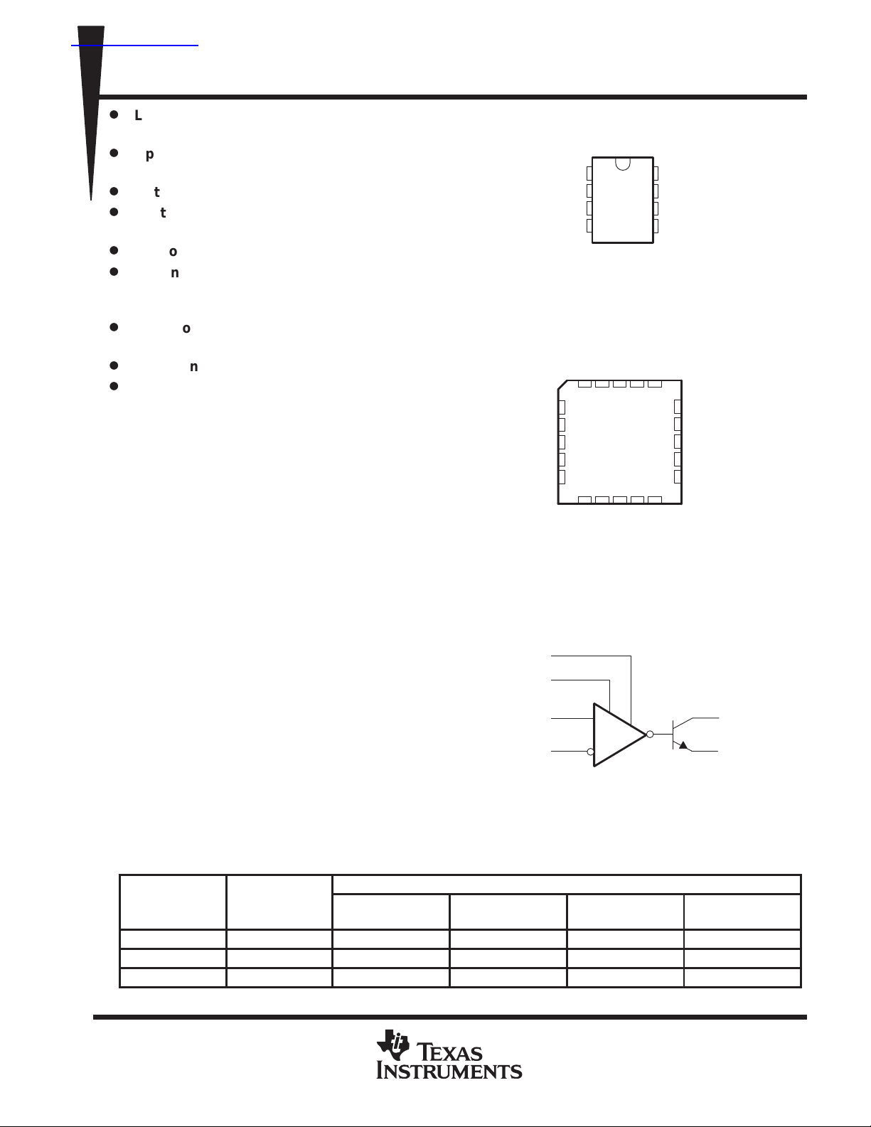
LP211, LP311 . . . D, JG, OR P PACKAGE
EMIT OUT
LP111...JG PACKAGE
(TOP VIEW)
1
IN+
2
IN–
3
V
CC –
NC
IN+
NC
IN–
NC
NC – No internal connection
4
LP111...FK PACKAGE
(TOP VIEW)
NC
EMIT OUT
NC
3 2 1 20 19
4
5
6
7
8
9 10 11 12 13
NC
NC
CC –
V
unctional block diagram
BALANCE
BAL / STRB
IN+
IN –
V
8
CC+
COL OUT
7
BAL / STRB
6
BALANCE
5
CC+
V
NC
NC
18
COL OUT
17
NC
16
BAL / STRB
15
NC
14
NC
BALANCE
COL OUT
EMIT OUT
AVAILABLE OPTIONS
PACKAGE
T
A
0 °C to 70 °C 7.5 mV LP311D — LP311JG LP311P
– 25 °C to 85 °C 7.5 mV LP211D — LP211JG LP211P
– 55 °C to 125 °C 7.5 mV — LP1 11FK LP111JG —
PRODUCTION DATA information is current as of publication date.
Products conform to specifications per the terms of Texas Instruments
standard warranty. Production processing does not necessarily include
testing of all parameters.
VIOmax AT 25°C
SMALL OUTLINE CERAMIC CERAMIC DIP PLASTIC DIP
(D) (FK) (JG) (P)
Copyright 1988, Texas Instruments Incorporated
POST OFFICE BOX 655303 • DALLAS, TEXAS 75265
1
LP111, LP211, LP311
LOW-POWER DIFFERENTIAL COMPARATORS WITH STROBES
SLCS003A – JUNE 1987 – REVISED MA Y 1988
absolute maximum ratings over operating free-air temperature range (unless otherwise noted)
Supply voltage, V
Supply voltage, V
Differential input voltage, V
Input voltage, V
Voltage from emitter output to V
Voltage from collector output to V
Voltage from collector output to emitter output 40 V. . . . . . . . . . . . . . . . . . . . . . . . . . . . . . . . . . . . . . . . . . . . . . . . .
Duration of output short circuit (see Note 4) 40 V. . . . . . . . . . . . . . . . . . . . . . . . . . . . . . . . . . . . . . . . . . . . . . . . . . .
Continuous total dissipation See Dissipation Rating Table. . . . . . . . . . . . . . . . . . . . . . . . . . . . . . . . . . . . . . . . . . .
Operating free-air temperature range, T
Storage temperature range – 65°C to 150°C. . . . . . . . . . . . . . . . . . . . . . . . . . . . . . . . . . . . . . . . . . . . . . . . . . . . . . .
Lead temperature range 1,6 mm (1/16 inch) from case for 10 seconds: D or P package 260°C. . . . . . . . . . .
Case temperature for 60 seconds: FK package 260°C. . . . . . . . . . . . . . . . . . . . . . . . . . . . . . . . . . . . . . . . . . . . . .
Lead temperature range 1,6 mm (1/16 inch) from case for 60 seconds: JG package 300°C. . . . . . . . . . . . . .
†
Stresses beyond those listed under absolute maximum ratings may cause permanent damage to the device. These are stress ratings only, and
functional operation of the device at these or any other conditions beyond those indicated in the recommended operating conditions section of this
specification is not implied. Exposure to absolute-maximum-rated conditions for extended periods may affect device reliability.
NOTES: 1. All voltage values, unless otherwise noted, are with respect to the midpoint between V
2. Differential input voltages are at IN+ with respect to IN –.
3. The magnitude of the input voltage must never exceed the magnitude of the supply voltage of ±15 V, whichever is less.
4. The output may be shorted to ground or to either power supply.
(see Note 1) 18 V. . . . . . . . . . . . . . . . . . . . . . . . . . . . . . . . . . . . . . . . . . . . . . . . . . . . . . . . . . .
CC+
(see Note 1) – 18 V. . . . . . . . . . . . . . . . . . . . . . . . . . . . . . . . . . . . . . . . . . . . . . . . . . . . . . . . .
CC–
(either input, see Notes 1 and 3) ±15 V. . . . . . . . . . . . . . . . . . . . . . . . . . . . . . . . . . . . . . . . . . . . .
I
(see Note 2) ±30 V. . . . . . . . . . . . . . . . . . . . . . . . . . . . . . . . . . . . . . . . . . . . . . . . . . .
ID
30 V. . . . . . . . . . . . . . . . . . . . . . . . . . . . . . . . . . . . . . . . . . . . . . . . . . . . . . . . .
CC –
40 V. . . . . . . . . . . . . . . . . . . . . . . . . . . . . . . . . . . . . . . . . . . . . . . . . . . . . . . .
CC –
: LP111 – 55°C to 125°C. . . . . . . . . . . . . . . . . . . . . . . . . . . . . . . . . . . .
A
LP211 – 25°C to 85°C. . . . . . . . . . . . . . . . . . . . . . . . . . . . . . . . . . . . . .
LP311 0°C to 70°C. . . . . . . . . . . . . . . . . . . . . . . . . . . . . . . . . . . . . . . .
CC+
and V
CC–
.
†
PACKAGE
D
FK
JG (LP111)
JG (LP_11)
P
TA ≤ 25°C
POWER RATING
500 mW
1375 mW
1050 mW
825 mW
500 mW
DERATING
FACTOR
5.8 mW/°C
11.0 mW/°C
8.4 mW/°C
6.6 mW/°C
8.0 mW/°C
recommended operating conditions
Input voltage (| V
Supply voltage, V
| ≤ 15 V) V
CC±
– V
CC+
CC –
DISSIPATION RATING TABLE
DERATE
ABOVE T
64°C
25°C
25°C
25°C
88°C
A
TA = 70°C
POWER RATING
464 mW
880 mW
672 mW
528 mW
500 mW
TA = 85°C
POWER RATING
377 mW
715 mW
546 mW
429 mW
500 mW
MIN MAX UNIT
+ 0.5 V
CC –
3.5 30 V
POWER RATING
CC+
TA = 125°C
—
275 mW
210 mW
—
—
– 1.5 V
2
POST OFFICE BOX 655303 • DALLAS, TEXAS 75265

VIDInput offset voltage
RS
100 kΩ
See Note 5
mV
ID
,
OL
,
25°C
0.4
1.5
S
6
,
0.1
0.4
IIOInput offset current
See Note 5
nA
IIBInput bias current
nA
Low-level strobe current
(strobe)
,
ID
,
25°C
100
300µA
A
gg g
R
kΩ
25°C
40
100
V/mV
LP111, LP211, LP311
LOW-POWER DIFFERENTIAL COMPARATORS WITH STROBES
SLCS003A – JUNE 1987 – REVISED MA Y 1988
electrical characteristics at specified free-air temperature, V
PARAMETER TEST CONDITIONS T
p
V
I
I
I
†
NOTES: 5. The offset voltages and offset currents given are the maximum values required to drive the output within 1 V of either supply with
Low-level output voltage
OL
p
p
Output off-state current VID > 10 mV, VCE = 35 V 25°C 0.2 100 nA
O(off)
Large signal differential voltage
VD
amplification
Supply current from V
CC+
Supply current from V
CC –
All typical values are at V
a 1-mA load. Thus, these parameters define an error band and take into account the worst-case effects of voltage gain and input
impedance.
6. Voltages are with respect to EMIT OUT and V
7. The strobe should not be shorted to ground; it should be current driven at 100 µA to 300 µA.
CC+
CC –
= ±15 V, TA = 25°C.
CC±
<
V
> 10 mV, I
See Note 6
VCC = 4.5 V, V
VID < –10 mV,
ee Note
V
See Note 7
= 5
L
VID = – 50 V, RL = ∞ Full range 150 300 µA
VID = 50 V, RL = ∞ Full range – 80 – 180 µA
,
= 0.3 V, V
CC –
= 25 mA,
= 0,
CC –
IOL = 1.6 mA,
< –10 mV,
tied together.
LP111 0.1 0.7
LP211,
LP311
= ±15 V (unless otherwise noted)
±
CC
A
25°C 2 7.5
Full range 10
°
Full range
25°C 2 25
Full range 35
25°C 15 100
Full range 150
°
°
MIN TYP†MAX UNIT
V
switching characteristics, V
PARAMETER TEST CONDITIONS MIN TYP MAX UNIT
Response time See Note 8 1.2 µs
NOTE 8: The response time is specified for a 100-mV input step with 5-mV overdrive.
CC
=
±
±5 V, T
= 25°C (unless otherwise noted)
A
POST OFFICE BOX 655303 • DALLAS, TEXAS 75265
3

IMPORTANT NOTICE
T exas Instruments and its subsidiaries (TI) reserve the right to make changes to their products or to discontinue
any product or service without notice, and advise customers to obtain the latest version of relevant information
to verify, before placing orders, that information being relied on is current and complete. All products are sold
subject to the terms and conditions of sale supplied at the time of order acknowledgement, including those
pertaining to warranty, patent infringement, and limitation of liability.
TI warrants performance of its semiconductor products to the specifications applicable at the time of sale in
accordance with TI’s standard warranty. T esting and other quality control techniques are utilized to the extent
TI deems necessary to support this warranty . Specific testing of all parameters of each device is not necessarily
performed, except those mandated by government requirements.
CERT AIN APPLICATIONS USING SEMICONDUCTOR PRODUCTS MAY INVOLVE POTENTIAL RISKS OF
DEATH, PERSONAL INJURY, OR SEVERE PROPERTY OR ENVIRONMENTAL DAMAGE (“CRITICAL
APPLICATIONS”). TI SEMICONDUCTOR PRODUCTS ARE NOT DESIGNED, AUTHORIZED, OR
WARRANTED TO BE SUITABLE FOR USE IN LIFE-SUPPORT DEVICES OR SYSTEMS OR OTHER
CRITICAL APPLICA TIONS. INCLUSION OF TI PRODUCTS IN SUCH APPLICATIONS IS UNDERST OOD TO
BE FULLY AT THE CUSTOMER’S RISK.
In order to minimize risks associated with the customer’s applications, adequate design and operating
safeguards must be provided by the customer to minimize inherent or procedural hazards.
TI assumes no liability for applications assistance or customer product design. TI does not warrant or represent
that any license, either express or implied, is granted under any patent right, copyright, mask work right, or other
intellectual property right of TI covering or relating to any combination, machine, or process in which such
semiconductor products or services might be or are used. TI’s publication of information regarding any third
party’s products or services does not constitute TI’s approval, warranty or endorsement thereof.
Copyright 1998, Texas Instruments Incorporated
 Loading...