

Page 1
SBOS301A − M AY 2004 − REVISED MARCH 2007
Please be aware that an important notice concerning availability, standard warranty, and use in critical applications of Texas Instruments
5
Single-Supply, High-Speed, Precision
LOGARITHMIC AMPLIFIER
LOG114
FEATURES
D ADVANTAGES:
− Tiny for High Density Systems
− Precision on One Supply
− Fast Over Eight Decades
− Fully-Tested Function
D TWO SCALING AMPLIFIERS
D WIDE INPUT DYNAMIC RANGE:
Eight Decades, 100pA to 10mA
D 2.5V REFERENCE
D STABLE OVER TEMPERATURE
D LOW QUIESCENT CURRENT: 10mA
D DUAL OR SINGLE SUPPLY: +5V, +5V
D PACKAGE: Small QFN-16 (4mm x 4mm)
D SPECIFIED TEMPERATURE RANGE:
−5°C to +75°C
APPLICATIONS
D ONET ERBIUM-DOPED FIBER OPTIC
AMPLIFIER (EDFA)
D LASER OPTICAL DENSITY MEASUREMENT
D PHOTODIODE SIGNAL COMPRESSION AMP
D LOG, LOG-RATIO FUNCTION
D ANALOG SIGNAL COMPRESSION IN FRONT
OF ANALOG-TO-DIGITAL (ADC) CONVERTER
D ABSORBANCE MEASUREMENT
DESCRIPTION
The LOG114 is specifically designed for measuring
low-level and wide dynamic range currents in
communications, lasers, medical, and industrial
systems. The device computes the logarithm or log-ratio
of an input current or voltage relative to a reference
current or voltage (logarithmic transimpedance
amplifier).
High precision is ensured over a wide dynamic range of
input signals on either bipolar (±5V) or single (+5V)
supply. Special temperature drift compensation circuitry
is included on-chip. In log-ratio applications, the signal
current may be from a high impedance source such as
a photodiode or resistor in series with a low impedance
voltage source. The reference current is provided by a
resistor in series with a precision internal voltage
reference, photo diode, or active current source.
The output signal at V
LOGOUT
out per decade of input current, which limits the output
so that it fits within a 5V or 10V range. The output can be
scaled and offset with one of the available additional
amplifiers, so it matches a wide variety of ADC input
ranges. Stable dc performance allows accurate
measurement of low-level signals over a wide
temperature range. The LOG114 is specified over a
−5°C to +75°C temperature range and can operate from
−40°C to +85°C.
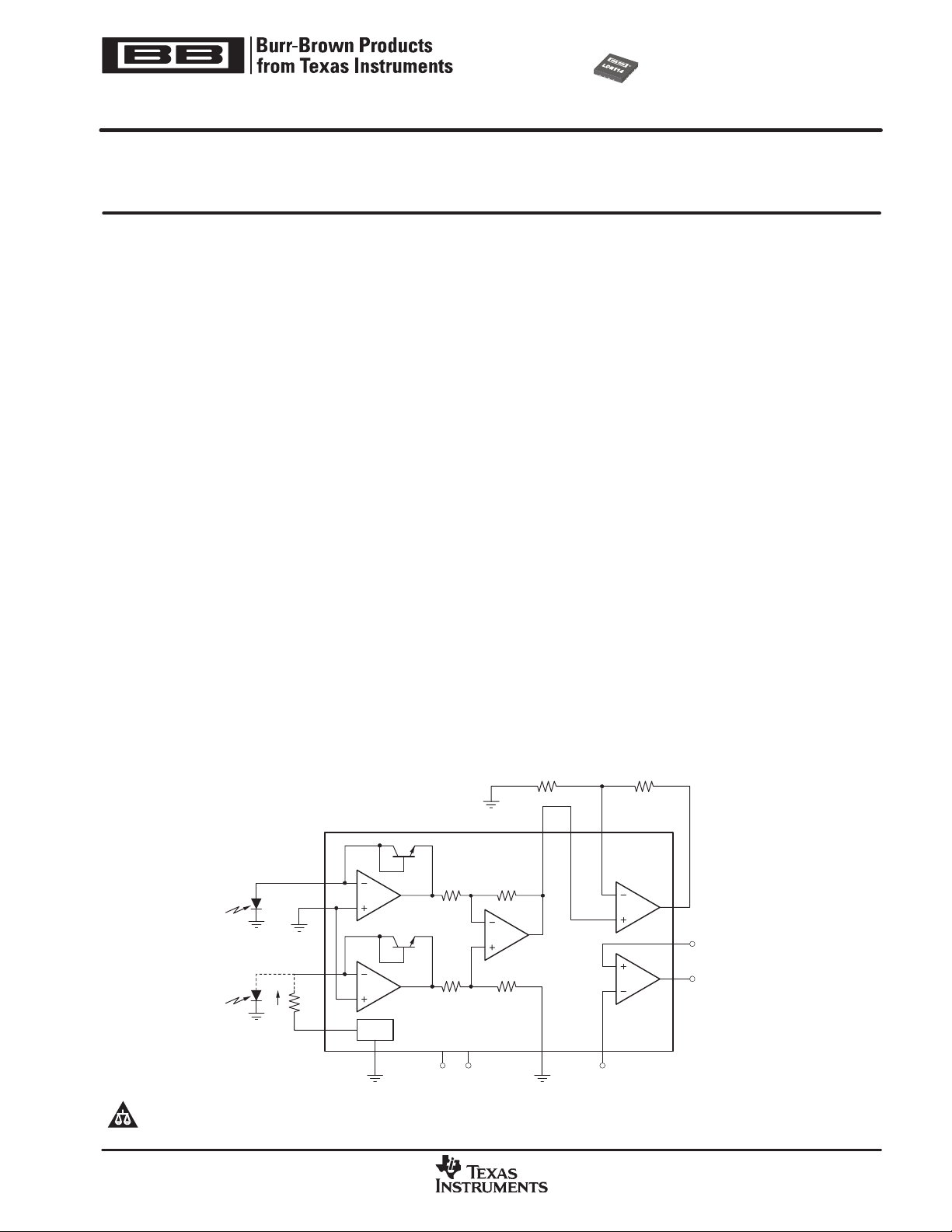
R
5
R
6
has a scale factor of 0.375V
−
+IN
IN
4
4
1110
LOG114
A
4
A
5
14
−
IN
5
(3)
V
O4
12
+IN
5
13
V
O5
15
NOTES: (1) Thermally dependent R1and R
provide temperature compensation.
(2) V
= 0.375×log(I1/I2).
LOGOUT
(3) VO4=0.375×K×log(I1/I2)
K=1+R6/R5.
(4) Differential A mplifier ( A3) Gai n = 6.2
I1and I2are current inp uts
from a photodiode
or other current source
I
REF
V
LOGOUT
(2)
9
Q
1
Ω
I
1
4
V
CMIN
5
I
2
3
R
REF
16
V
REF
2.5V
A
1
A
2
REF
186 7
REF GND
200
(1)
R
1
Q
2
Ω
200
(1)
R
3
V
V+
Ω
1250
R
2
(4)
A
3
Ω
1250
R
4
−
ComV
semiconductor products and disclaimers thereto appears at the end of this data sheet.
All trademarks are the property of their respective owners.
! !
www.ti.com
Copyright 2004−2007, Texas Instruments Incorporated
3
Page 2

"#$$%
SBOS301A − M AY 2004 − REVISED MARCH 2007
www.ti.com
ABSOLUTE MAXIMUM RATINGS
(1)
Supply Voltage, V+ to V− 12V. . . . . . . . . . . . . . . . . . . . . . . . . . . . . . .
Current
(2)
(V−) −0.5V to (V+) + 0.5V. . . . .
(2)
±10mA. . . . . . . . . . . . . . . . . . . .
Signal Input Terminals, Voltage
Output Short-Circuit
(3)
Continuous. . . . . . . . . . . . . . . . . . . . . . . . . .
Operating Temperature −40°C to +85°C. . . . . . . . . . . . . . . . . . . . . .
Storage Temperature −55°C to +125°C. . . . . . . . . . . . . . . . . . . . . . .
proper handling and installation procedures can cause damage.
ESD damage can range from subtle performance degradation to
complete device failure. Precision integrated circuits may be more
susceptible t o damage because very small parametric changes could
cause the device not to meet its published specifications.
This integrated circuit can be damaged by ESD. Texas
Instruments recommends that all integrated circuits be
handled with appropriate precautions. Failure to observe
Junction Temperature +150°C. . . . . . . . . . . . . . . . . . . . . . . . . . . . . . .
ESD Rating (Human Body Model) 2000V. . . . . . . . . . . . . . . . . . . .
(1)
Stresses above these ratings may cause permanent damage.
PRECISION CURRENT MEASUREMENT
PRODUCTS
Exposure to absolute maximum conditions for extended periods
may degrade device reliability. These are stress ratings only , an d
functional operation of the device at these or any other conditions
beyond those specified is not implied.
(2)
Input terminals are diode-clamped to the power-supply rails.
Input signals that can swing more than 0.5V beyond the supply
rails should be current-limited to 10mA or less.
(3)
Short-circuit to ground.
ORDERING INFORMATION
(1)
FEATURES PRODUCT
Logarithmic Transimpedance Amplifier, 5V, Eight Decades LOG114
Logarithmic Transimpedance, 36V, 7.5 Decades LOG112
Resistor-Feedback Transimpedance, 5V, 5.5 Decades
Switched Integrator Transimpedance, Six Decades
Direct Digital Converter, Six Decades
OPA380,
OPA381
IVC102
DDC112
PRODUCT PACKAGE-LEAD PACKAGE DESIGNATOR PACKAGE MARKING
LOG114 QFN-16 RGV LOG114
(1)
For the most current package and ordering information, see the Package Option Addendum at the end of this document, or see the TI web site
at www .ti.com.
PIN CONFIGURATION
T op View
V
REF GND
NC
5
REFVO5
V
16
15 14 13
1
Exposed
2
3
I
2
4
I
1
thermal
diepad on
underside
(Must be
connected to V−)
5
6
−
V
CM IN
V
QFN−16 (4mm x 4mm)
NC = NoConnection
5
IN
−
+IN
78
V+
Com
12
V
O4
11
−
IN
4
10
+IN
4
9
V
LOGOUT
QFN-16
2
Page 3

"#$$%
www.ti.com
SBOS301A − MAY 2004 − REVISED MARCH 2007
ELECTRICAL CHARACTERISTICS: VS = +5V
Boldface limits apply over the specified temperature range, TA = −5°C to +75°C.
All specifications at TA = +25°C, R
PARAMETER CONDITIONS MIN TYP MAX UNITS
CORE LOG FUNCTION IIN/V
LOG CONFORMITY ERROR
(1)
Initial 1nA to 100µA (5 decades) 0.1 0.2 %
Over Temperature 1nA to 100µA (5 decades) 0.1 0.4 %
TRANSFER FUNCTION (GAIN)
(2)
Initial Scaling Factor 100pA to 10mA 0.375 V/decade
Scaling Factor Error 1nA to 100µA 0.4 ±2.5 %
Over Temperature T
INPUT, A1 and A
2
Offset V oltage V
vs Temperature dV/dT T
vs Power Supply PSRR VS = ±2.25V to ±5.5V 75 400 µV/V
Input Bias Current I
vs Temperature T
Input Common-Mode Voltage Range V
Voltage Noise e
Current Noise i
OUTPUT, A3 (V
Output Offset, V
)
LOGOUT
, Initial V
OSO
Over Temperature T
Full-Scale Output (FSO)
(3)
Gain Bandwidth Product GBW IIN = 1µA 50 MHz
Short-Circuit Current I
Capacitive Load 100 pF
OP AMP, A4 and A
5
Input Offset Voltage V
vs Temperature dV/dT T
vs Supply PSRR VS = ±4.5V to ±5.5V 30 250 µV/V
vs Common-Mode Voltage CMRR 74 dB
Input Bias Current I
Input Offset Current I
Input Voltage Range (V−) (V+) − 2 V
Input Noise f = 0.1Hz to 10Hz 2 µV
f = 1kHz 13 nV/√Hz
Current Noise i
Open-Loop Voltage Gain A
Gain Bandwidth Product GBW 15 MHz
Slew Rate SR 5 V/µs
Settling Time 0.01% t
Rated Output (V−) + 0.5 (V+) − 0.5 V
Short-Circuit Current I
= 10kΩ, VCM = GND, unless otherwise noted.
VLOGOUT
OUT
100pA to 3.5mA (7.5 decades) 0.9 %
1mA to 10mA See Typical Characteristics
100pA to 3.5mA (7.5 decades) 0.5 %
1mA to 10mA See Typical Characteristics %
MIN
+15°C to +50°C 0.7 ±3 %
OS
MIN
B
MIN
CM
n
f = 0.1Hz to 10kHz 3 µVrms
f = 1kHz 30 nV/√Hz
f = 1kHz 4 fA/√Hz
MIN
MIN
OSO
SC
OS
OS
SC
n
B
n
OL
G = −1, 3V Step, CL = 100pF 1.5 µs
S
LOG114
Equation VO = (0.375V) Log (I1/I2) V
0.009 0.017 dB
0.08 dB
0.035 0.21 dB
to T
MAX
1.5 ±3.5 %
±1 ±4 mV
to T
MAX
+15 µV/°C
±5 pA
to T
MAX
Doubles every 10°C
(V−)+1.5 to
(V+)−1.5
±11 ±50 mV
to T
MAX
±15 ±65 mV
(V−) + 0.6 (V+) − 0.6 V
±18 mA
±250 ±1000 µV
to T
MAX
±2 µV/°C
−1 µA
±0.05 µA
2 pA/√Hz
100 dB
+4/−10 mA
V
PP
3
Page 4

"#$$%
www.ti.com
SBOS301A − MAY 2004 − REVISED MARCH 2007
ELECTRICAL CHARACTERISTICS: VS = +5V (continued)
Boldface limits apply over the specified temperature range, TA = −5°C to +75°C.
All specifications at TA = +25°C, R
PARAMETER UNITSMAXTYPMINCONDITIONS
TOTAL ERROR
FREQUENCY RESPONSE, Core Log
BW, 3dB I1 or I2 = IAC = 10% of IDC value, I
1nA 5 kHz
10nA 12 kHz
100nA 120 kHz
1µA 2.3 MHz
10µA to 1mA (ratio 1:100) > 5 MHz
1mA to 3.5mA (ratio 1:3.5) > 5 MHz
3.5mA to 10mA (ratio 1:2.9) > 5 MHz
Step Response I
Increasing (I1 or I2)
8nA to 240nA (ratio 1:30) 0.7 µs
10nA to 100nA (ratio 1:10) 1.5 µs
10nA to 1µA (ratio 1:100) 0.15 µs
10nA to 10µA (ratio 1:1k) 0.07 µs
10nA to 1mA (ratio 1:100k) 0.06 µs
1mA to 10mA (ratio 1:10) 1 µs
Decreasing (I1 or I2) I
8nA to 240nA (ratio 1:30) 1 µs
10nA to 100nA (ratio 1:10) 2 µs
10nA to 1µA (ratio 1:100) 0.25 µs
10nA to 10µA (ratio 1:1k) 0.05 µs
10nA to 1mA (ratio 1:100k) 0.03 µs
1mA to 10mA (ratio 1:10) 1 µs
VOLTAGE REFERENCE
Bandgap Voltage 2.5 V
Error, Initial ±0.15 ±1 %
vs Temperature ±25 ppm/°C
vs Supply VS = ±4.5V to ±5.5V ±30 ppm/V
vs Load IO = ±2mA ±200 ppm/mA
Short-Circuit Current ±10 mA
POWER SUPPL Y
Dual Supply Operating Range V
Quiescent Current I
TEMPERATURE RANGE
Specification, T
Operating −40 +85 °C
Storage −55 +125 °C
Thermal Resistance, q
(1)
Log conformity error is peak deviation from the best-fit straight line of V
K, equals 0.375V output per decade of input current.
(2)
Scale factor of core log function is trimmed to 0.375V output per decade change of input current.
(3)
Specified by design.
(4)
Worst-case total error for any ratio of I
(5)
Total error includes offset voltage, bias current, gain, and log conformity.
(6)
Small signal bandwidth (3dB) and transient response are a function of the level of input current. Smaller input current amplitude results in lower bandwidth.
(4, 5)
MIN
to T
MAX
JA
= 10kΩ, VCM = GND, unless otherwise noted.
VLOGOUT
(6)
REF
REF
S
Q
, as the largest of the two errors, when I, and I2 are considered separately.
1/I2
LOG114
See Typical Characteristics
= 1µA
REF
= 1µA
= 1µA
±2.4 ±5.5 V
IO = 0 ±10 ±15 mA
−5 +75 °C
62 °C/W
vs Log (I1/I2) curve expressed as a percent of peak-to-peak full-scale output. Scale factor,
O
4
Page 5

"#$$%
www.ti.com
SBOS301A − MAY 2004 − REVISED MARCH 2007
ELECTRICAL CHARACTERISTICS: VS = +5V
Boldface limits apply over the specified temperature range, TA = −5°C to +75°C.
All specifications at TA = +25°C, R
PARAMETER CONDITIONS MIN TYP MAX UNITS
CORE LOG FUNCTION IIN/V
LOG CONFORMITY ERROR
(1)
Initial 1nA to 100µA (5 decades) 0.1 0.25 %
Over Temperature 1nA to 100µA (5 decades) 0.1 0.4 %
TRANSFER FUNCTION (GAIN)
(2)
Initial Scaling Factor 10nA to 100µA 0.375 V/decade
Scaling Factor Error 1nA to 100µA 0.4 ±2.5 %
Over Temperature T
INPUT, A1 and A
2
Offset V oltage V
vs Temperature dV/dT T
vs Power Supply PSRR VS = +4.5V to +5.5V 300 µV/V
Input Bias Current I
vs Temperature T
Input Common-Mode Voltage Range V
Voltage Noise e
Current Noise i
OUTPUT, A3 (V
Output Offset, V
)
LOGOUT
, Initial V
OSO
Over Temperature T
Full Scale Output (FSO)
(3)
Gain Bandwidth Product GBW IIN = 1µA 50 MHz
Short-Circuit Current I
Capacitive Load 100 pF
OP AMP, A4 and A
5
Input Offset Voltage V
vs Temperature dV/dT T
vs Supply PSRR VS = +4.8V to +5.5V 30 µV/V
vs Common-Mode Voltage CMRR 70 dB
Input Bias Current I
Input Offset Current I
Input Voltage Range (V−) (V+) − 1.5 V
Input Noise f = 0.1Hz to 10Hz 1 µV
f = 1kHz 28 nV/√Hz
Current Noise i
Open-Loop Voltage Gain A
Gain Bandwidth Product GBW 15 MHz
Slew Rate SR 5 V/µs
Settling Time 0.01% t
Rated Output (V−) + 0.5 (V+) − 0.5 V
Short-Circuit Current I
= 10kΩ, VCM = +2.5V, unless otherwise noted.
VLOGOUT
OUT
100pA to 3.5mA (7.5 decades) 0.9 %
1mA to 10mA See Typical Characteristics
100pA to 3.5mA (7.5 decades) 0.5 %
1mA to 10mA See Typical Characteristics
MIN
+15°C to +50°C 0.7 ±3 %
OS
MIN
B
MIN
CM
n
f = 0.1Hz to 10kHz 3 µVrms
f = 1kHz 30 nV/√Hz
n
OSO
f = 1kHz 4 fA/√Hz
MIN
VS = +5V (V−) + 0.6 (V+) − 0.6 V
SC
OS
MIN
B
OS
n
OL
G = −1, 3V Step, CL = 100pF 1.5 µs
S
SC
LOG114
Equation VO = (0.375V) Log (I1/I2) + V
0.009 0.022 dB
0.08 dB
0.0.35 0.21 dB
to T
MAX
0.035 ±3.5 %
±1 ±7 mV
to T
MAX
+30 µV/°C
±5 pA
to T
MAX
Doubles every 10°C
(V−)+1.5 to
(V+)−1.5
±14 ±65 mV
to T
MAX
±18 ±80 mV
±18 mA
±250 ±4000 µV
to T
MAX
±2 µV/°C
−1 µA
±0.05 µA
2 pA/√Hz
100 dB
+4/−10 mA
CM
V
V
PP
5
Page 6

"#$$%
www.ti.com
SBOS301A − MAY 2004 − REVISED MARCH 2007
ELECTRICAL CHARACTERISTICS: VS = +5V (continued)
Boldface limits apply over the specified temperature range, TA = −5°C to +75°C.
All specifications at TA = +25°C, R
PARAMETER UNITSMAXTYPMINCONDITIONS
TOTAL ERROR
FREQUENCY RESPONSE, Core Log
BW, 3dB I1 or I2 = IAC = 10% of IDC value, I
1nA 5 kHz
10nA 12 kHz
100nA 120 kHz
1µA 2.3 MHz
10µA to 1mA (ratio 1:100) > 5 MHz
1mA to 3.5mA (ratio 1:3.5) > 5 MHz
3.5mA to 10mA (ratio 1:2.9) > 5 MHz
Step Response I
Increasing (I1 or I2)
8nA to 240nA (ratio 1:30) 0.7 µs
10nA to 100nA (ratio 1:10) 1.5 µs
10nA to 1µA (ratio 1:100) 0.15 µs
10nA to 10µA (ratio 1:1k) 0.07 µs
10nA to 1mA (ratio 1:100k) 0.06 µs
1mA to 10mA (ratio 1:10) 1 µs
Decreasing (I1 or I2) I
8nA to 240nA (ratio 1:30) 1 µs
10nA to 100nA (ratio 1:10) 2 µs
10nA to 1µA (ratio 1:100) 0.25 µs
10nA to 10µA (ratio 1:1k) 0.05 µs
10nA to 1mA (ratio 1:100k) 0.03 µs
1mA to 10mA (ratio 1:10) 1 µs
VOLTAGE REFERENCE
Bandgap Voltage 2.5 V
Error, Initial ±0.15 ±1 %
vs Temperature ±25 ppm/°C
vs Supply VS = +4.8V to +11V ±30 ppm/V
vs Load IO = ±2mA ±200 ppm/mA
Short-Circuit Current ±10 mA
POWER SUPPL Y
Single Supply Operating Range V
Quiescent Current I
TEMPERATURE RANGE
Specification, T
Operating −40 +85 °C
Storage −55 +125 °C
Thermal Resistance, q
(1)
Log conformity error is peak deviation from the best-fit straight line of V
K, equals 0.375V output per decade of input current.
(2)
Scale factor of core log function is trimmed to 0.375V output per decade change of input current.
(3)
Specified by design.
(4)
Worst-case total error for any ratio of I
(5)
Total error includes offset voltage, bias current, gain, and log conformity.
(6)
Small signal bandwidth (3dB) and transient response are a function of the level of input current. Smaller input current amplitude results in lower bandwidth.
(4, 5)
MIN
to T
MAX
JA
= 10kΩ, VCM = +2.5V, unless otherwise noted.
VLOGOUT
(6)
REF
REF
S
Q
, as the largest of the two errors, when I, and I2 are considered separately.
1/I2
LOG114
See Typical Characteristics
= 1µA
REF
= 1µA
= 1µA
4.8 11 V
IO = 0 ±10 ±15 mA
−5 +75 °C
62 °C/W
vs Log (I1/I2) curve expressed as a percent of peak-to-peak full-scale output. Scale factor,
O
6
Page 7

www.ti.com
TYPICAL CHARACTERISTICS: VS = +5V
All specifications at TA = +25°C, R
= 10kΩ, VCM = GND, unless otherwise noted.
VLOGOUT
"#$$%
SBOS301A − MAY 2004 − REVISED MARCH 2007
2.0
NORMALIZED TRANSFER FUNCTION
1.5
1.0
0.5
0
−
0.5
−
1.0
Normalized Output Voltage (V)
−
1.5
−
2.0
−410−310−210−1
10
SCALING FACTOR ERROR (I
40
30
20
+70_C
10
0
Gain Error (%)
−
10
−
20
0_C
+80_C
+90_C
1nA 10nA 100nA 1µA10µA100µA 1mA 10mA100pA
Current Ratio (I1/I2)
+25_C
−10_
C
Input Current (I
110110210
= reference 100pA to 10mA)
2
)
1
ONE CYCLE OF NORMALIZED TRANSFER FUNCTION
0.40
0.35
0.30
0.25
0.20
0.15
0.10
Normalized Output Voltage (V)
0.05
3
4
10
0
110
Current Ratio (I1/I2)
vs I1INPUT (I2=1µA)
V
2.5
LOGOUT
2.0
1.5
1.0
0.5
(V)
0
−
LOGOUT
0.5
V
−
1.0
−
1.5
−
2.0
−
2.5
1nA 10nA 100nA 1µA10µA100µA 1mA 10mA100pA
Input Current (I
)
1
vs I2INPUT (I1=1µA)
V
2.0
LOGOUT
1.5
1.0
0.5
(V)
0
−
0.5
LOGOUT
V
−
1.0
−
1.5
−
2.0
−
2.5
1nA 10nA 100nA 1µA10µA100µA1mA100pA
Input Current (I
)
1
10mA
4
3
2
1
(V)
1µA
100nA
0
LOGOUT
−
1
V
−
2
−
3
−
4
1nA 10nA 100nA 1µA10µA 100µA 1mA 10mA100pA
V
LOGOUT
10nA
10mA
I
REF(I2
vs I
1nA
1mA
REF
100pA
10µA
100µA
)
7
Page 8

"#$$%
SBOS301A − MAY 2004 − REVISED MARCH 2007
TYPICAL CHARACTERISTICS: VS = +5V (continued)
All specifications at TA = +25°C, R
= 10kΩ, VCM = GND, unless otherwise noted.
VLOGOUT
www.ti.com
100
80
60
40
20
0
−
20
Total Error(mV)
−
40
−
60
I1=10nA
−
80
−
100
100
80
60
40
20
0
−
20
Total Error(mV)
−
40
−
60
−
80
−
100
AVERAGETOTALERRORAT +80_C
I1=10µA
I1=1nA I1= 100nA I1=1µA
400µA 600µA 800µA
AVERAGE TOTALERRORAT−10_C
I1= 10nA
I1=100µA
I1=10µA
400µA 600µA 800µA
I
2
I
2
I1=1mA
I1=100µA
I1=1mA
I1= 100nA
I1=1nA
I1=1µA
100
80
60
40
20
0
−
20
Total Error(mV)
−
40
−
60
−
80
−
100
1mA100µA 200µA
1.4
1.2
1.0
0.8
0.6
Linearity (%)
0.4
0.2
1mA100µA 200µA
0
−
100102030405060708090
AVERAGETOTALERRORAT +25_C
I1=1mA
I1=100µA
I1=1µA
400µA 600µA 800µA
LOG CONFORMITY vsTEMPERATURE
7.5Decade
6Decade
Temperature(_C)
I
2
4Decade
I1=10µA
5 Decade
I1= 1nA, 10nA,
100nA
1mA100µA 200µA
7 Decade
0.09
0.08
0.07
0.06
Linearity (%)
0.05
0.04
4 DECADE LOG CONFORMITY vs I
+90_C
+80_C
1nA 10nA 100nA 1µA10µA 100µA 1mA 10mA100pA
I
)
REF(I1
−10_
C
+25_C
REF
0_C
+70_C
0.40
0.35
0.30
0.25
0.20
0.15
Linearity (%)
0.10
0.05
0
5 DECADE LOG CONFORMITY vs I
+90_C
+80_C
+70_C
−10_
C, 0_C, +25_C
1nA 10nA 100nA 1µA10µA100µA 1mA 10mA100pA
I
)
REF(I1
REF
8
Page 9

www.ti.com
TYPICAL CHARACTERISTICS: VS = +5V (continued)
All specifications at TA = +25°C, R
level.
VLOGOUT
= 10kΩ, VCM = GND, unless otherwise noted. For ac measurements, small signal means up to approximately 10% of dc
"#$$%
SBOS301A − MAY 2004 − REVISED MARCH 2007
0.45
6 DECADE LOG CONFORMITY vs I
REF
0.40
+90_C
0.35
0.30
Linearity (%)
+80_C
+70_C
Linearity (%)
0.25
−10_
C, 0_C, +25_C
0.20
1nA 10nA 100nA 1µA10µA100µA 1mA 10mA100pA
I
)
REF(I1
20
SMALL−SIGNAL V
LOGOUT
10mA
10
(%)
0
LOGOUT
−
10
−
20
Normalized V
−
30
−
40
10nA
1µA
100nA
100µA
1mA
10µA
Normalized LOG Output (dB)
100 1k 10k 100k 1M 10M 100M10
Frequency (Hz)
8 DECADE LOG CONFORMITY (100pA to 3.5mA)
1.6
1.5
1.4
+90_C
1.3
1.2
1.1
0_C
+70_C
+80_C
1.0
0.9
1nA 10nA 100nA 1µA10µA100µA 1mA 10mA100pA
Input Current (I
SMALL−SIGNALAC RESPONSE I
0
−
5
−
10
−
15
−
20
−
25
−
30
−
35
−
40
−
45
−
50
(10% sine modulation)
1nA 1mA
10nA
100nA
1k 10k 100k 1M 10M 100M100
Frequency (Hz)
1
1µA
or I2)
−10_
10µA
+25_C
C
1
100µA
SMALL−SIGNALAC RESPONSE I
0
−
5
−
10
−
15
−
20
−
25
−
30
−
35
−
40
Normalized LOG Output (dB)
−
45
−
50
(10% sine modulation)
1nA
10nA
1µA
100nA
1k 10k 100k 1M 10M 100M100
Frequency (Hz)
10µA
2
1mA
100µA
GAIN AND PHASE vs FREQUENCY
A
160
3
225
140
120
180
100
80
60
Gain
40
Gain (dB)
Phase
135
90
)
_
Phase(
20
0
−
20
−
40
1M 10M
45
0
40M100 1k 10k 100k
Frequency (Hz)
9
Page 10

"#$$%
SBOS301A − M AY 2004 − REVISED MARCH 2007
TYPICAL CHARACTERISTICS: VS = +5V (continued)
All specifications at TA = +25°C, R
and A5GAINAND PHASE vsFREQUENCY
A
140
120
100
80
60
Gain (dB)
40
20
0
−
20
4
Gain
= 10kΩ, VCM = GND, unless otherwise noted.
VLOGOUT
Phase
100k 1M
Frequency (Hz)
10M 18M1101001k10k
180
135
90
45
0
and A5NONINVERTING CLOSED−LOOP RESPONSE
A
4
3
0
−
)
_
Phase(
3
−
6
−
9
Normalized Output (dB)
−
12
−
15
www.ti.com
G=1
G=10
100M1k 10k 100k 1M 10M
Frequency (Hz)
andA5CAPACITIVE LOAD RESPONSE
G=+1
A
4
C = 100pF
C<10pF
100k 1M 10M
Frequency (Hz)
50M1k 10k
A
and A5INVERTING CLOSED−LOOPRESPONSE
4
30
20
10
0
−
10
−
20
−
30
Gain (dB)
−
40
−
50
−
60
−
70
−
80
10k 60M1k
G=−10
G=−1
100k 1M 10M
Frequency (Hz)
10
0
−
10
−
20
Gain (dB)
−
30
−
40
−
50
10
Page 11

www.ti.com
"#$$%
SBOS301A − MAY 2004 − REVISED MARCH 2007
APPLICATIONS INFORMATION
OVERVIEW
The LOG114 is a precision logarithmic amplifier that is
capable of measuring currents over a dynamic range of
eight decades. It computes the logarithm, or log ratio,
of an input current relative to a reference current according to equation (1).
I
1
ǒ
V
The output at V
+ 0.375 log
LOGOUT
LOGOUT
for an ADC input using an uncommitted or external op
amp.
An offsetting voltage (V
Com pin to raise the voltage at V
offsetting voltage is used, the transfer function
becomes:
V
+ 0.375 log
LOGOUT
Ǔ
10
I
2
(1)
can be digitized directly , or scaled
) can be connected to the
Com
LOGOUT
I
1
ǒ
Ǔ
) V
10
I
2
Com
. When an
(2)
Either I1 or I2 can be held constant to serve as the reference current, with the other input being used for the input signal. The value of the reference current is selected
such that the output at V
LOGOUT
(pin 9) is zero when the
reference current and input current are equal. An onchip 2.5V reference is provided for use in generating the
reference current.
Two additional amplifiers, A4 and A5, are included in the
LOG114 for use in scaling, offsetting, filtering, threshold
detection, or other functions.
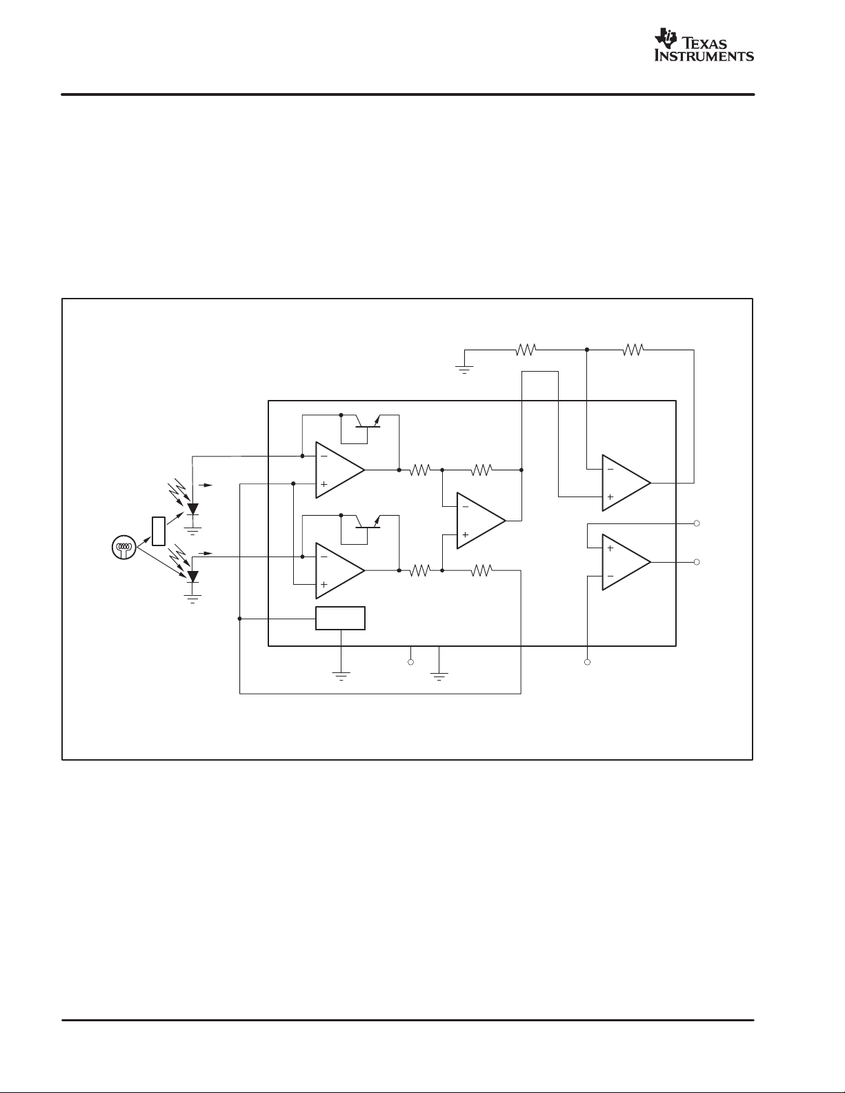
BASIC CONNECTIONS
Figure 1 and Figure 2 show the LOG114 in typical dual
and single-supply configurations, respectively. To reduce the influence of lead inductance of power-supply
lines, it is recommended that each supply be bypassed
with a 1 0 µF tantalum capacitor in parallel with a 1000pF
ceramic capacitor as shown in Figure 1 and Figure 2.
Connecting these capacitors as close to the LOG114
V+ supply pin to ground as possible improves supply−
related noise rejection.
R
REF
2.5M
I
REF
1µF
Input Signa l
100pAto 10m A
Ω
R
7
100k
Ω
R
5
100k
9
(1)
V
1000pF
µ
LOGOUT
R
2
A
3
R
4
F
Q
1
I
4
1
A
V
REF GND
A
2.5V
1
1
Q
2
2
REF
V
CM IN
5
I
3
2
V
16
REF
R
1
R
3
V+
86 7
1000pF
10µF10
++
+5V
V−
5V
−
+IN
Com
56.2k
Ω
1110
IN
−
4
4
IN
−
5
14
NOTE: (1) V
(2) V
R
8
Ω
R
6
66.5k
Ω
LOG114
(2)
V
O4
A
4
+IN
5
V
A
LOGOUT
=−0.249×log(I1/I2)+1.5V
O4
O5
5
= 0. 375×log(I1/I2)
12
13
15
Figure 1. Dual Supply Configuration Example for Best Accuracy Over Eight Decades.
11
Page 12

"#$$%
SBOS301A − M AY 2004 − REVISED MARCH 2007
www.ti.com
REF3040
or
REF3240
4.096V
Reference
Input current
from photodiode
or current source
Photodiode
(4)
I
IµA
R
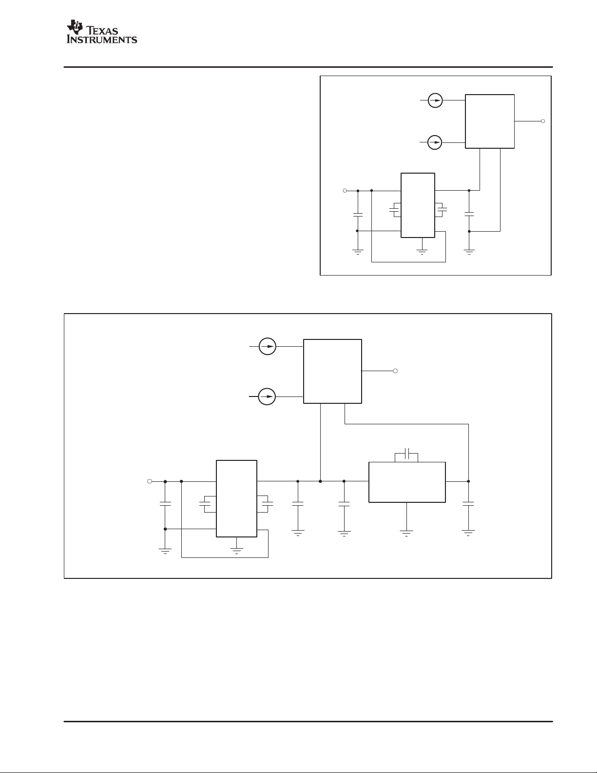
REF
1.62M
+2.5V
R
5
Ω
100k
R
7
Ω
100k
R
8
Ω
316k
+IN
V
4
Com
1110
−
IN
4
−
IN
5
1
= +2.5V
9
(2)
V
+
A
10µF
LOGOUT
R
2
3
R
4
−
V
Com
Q
1
I
1
4
A
(1)
V
CM IN
Ω
I
2
5
I
2
3
A
V
16
REF
V
REF GND
2.5V
1
R
1
1
Q
2
R
3
2
REF
V
1
867
1000pF
+5V
66.5k
A
4
A
5
R
6
Ω
LOG114
(3)
V
12
O4
+IN
5
13
V
O5
15
NOTE: (1) In single−supply configuration, V
(2) V
(3) V
(4) The cathode of the photodiode is returned to V
= 0.375×log(I1/I2)+2.5V.
LOGOUT
=−0.249×log(I1/I2)+1.5V.
O4
could be returned to a voltage more positive than V
photodiode capacitance, which increases speed.
must be connected to≥1V.
CM IN
resultinginzerobiasacrossit.Thecathode
REF
CM IN
to create a reverse bias for reducing
Figure 2. Single-Supply Configuration Example for Measurement Over Eight Decades.
12
Page 13

www.ti.com
"#$$%
SBOS301A − M AY 2004 − REVISED MARCH 2007
DESIGN EXAMPLE FOR DUAL-SUPPLY
CONFIGURATION
Given these conditions:
D V+ = 5V and V− = −5V
D 100pA ≤ Input signal
D The stage following the LOG114 is an analog-to-
digital converter (ADC) with +5V supply and
+2.5V reference voltage, so VO4 swings from
+0.5V to +2.5V.
1. Due to LOG114 symmetry, you can choose either
I1 or I2 as the signal input pin. Choosing I1 as the
reference makes the resistor network around A4
simpler. (Note: Current must flow into pins 3 (I1) and
pin 4 (I2).)
2. Select the magnitude of the reference current.
Since the signal (I2) spans eight decades, set I1 to
1µA − four decades above the minimum I2 value.
(Note that it does not have to be placed in the
middle. If I2 spanned seven decades, I1 could be set
three decades above the minimum and four
decades below the maximum I2 value.) This
configuration results in more swing amplitude in the
negative direction, which provides more sensitivity
(∆VO4 per ∆I2) when the current signal decreases.
4. The A
amplifier scales and offsets the V
4
LOGOUT
signal for use by the ADC using the equation:
VO4+*S
FACTOR
ǒ
V
LOGOUT
Ǔ
) V
OFFSET
(5)
The A4 amplifier is specified with a rated output swing
capability from (V−) +0.5V to (V+) − 0.5V.
Therefore, choose the final A4 output:
0V ≤ VO4 ≤ +2.5V
This output results in a 2.5V range for the 3V V
LOGOUT
range, or 2.5V/3V scaling factor.
5. When I2 = 10mA, V
LOGOUT
= −1.5V. Using the
equation in step 5:
VO4+*S
FACTOR
ǒ
V
0V +*2.5Vń3V(*1.5V) ) V
Therefore, V
OFFSET
= 0V
The A4 amplifier configuration for VO4 = −2.5/3(V
LOGOUT
Ǔ
) V
OFFSET
OFFSET
(6)
LOGOUT
+ 0V is seen in Figure 3.
The overall transer function is:
I
1
ǒ
VO4+*0.249 log
Ǔ
I
2
) 1.5V
(7)
)
3. Using Equation (1) calculate the expected range of
log outputs at V
For I2+ 10mA :
V
+ 0.375 log
For I2+ 100pA :
V
+ 0.375 log
LOGOUT
LOGOUT
+ 0.375 log
+ 0.375 log
LOGOUT
ǒ
ǒ
1mA
10mA
1mA
100pA
:
I
1
ǒ
Ǔ
I
2
Ǔ
+*1.5V
I
1
ǒ
Ǔ
I
2
Ǔ
+)1.5V
(3)
Therefore, the expected voltage range at the output
of amplifier A3 is:
* 1.5V v V
LOGOUT
v)1.5V
(4)
Internal A4Output Amplifier
R
5
Ω
V
LOGOUT
V
REF
+2.5V
amplifierusedtoscaleandoffsetV
A
4
100k
R
100k
7
Ω
82.5k
+5V
A
4
−
37.4k
R
6
Ω
VO4=−2/3 (V
I
5V
R
8
Ω
LOGOUT
2
100pA
0V +2.5V
V
O4
for 0V to 2.5V output.
LOGOUT
10mA
)
Figure 3. Operational Amplifier Configuration for
Scaling the Output Going to ADC Stage.
13
Page 14

"#$$%
SBOS301A − M AY 2004 − REVISED MARCH 2007
www.ti.com
DESIGN EXAMPLE FOR SINGLE-SUPPLY
CONFIGURATION
Given these conditions:
D V+ = 5V
D V− = GND
D 100pA ≤ Input signal ≤ 10mA
D The stage following the LOG114 is an analog to
digital converter (ADC) with +5V supply and
+2.5V reference voltage
1. Choose either I1 or I2 as the signal input pin. For this
example, I2 is used. Choosing I1 as the reference
current makes the resistor network around A4
simpler. (Note: Current only flows into the I1 and I
pins.)
2. Select the magnitude of the reference current.
Since the signal (I2) spans eight decades, set I1 to
1µA − four decades above the minimum I2 value,
and four decades below the maximum I2 value.
(Note that it does not have to be placed in the
middle. If I2 spanned seven decades, I1 could be set
three decades above the minimum and four
decades below the maximum I2 value.) This
configuration results in more swing amplitude in the
negative direction, which provides more sensitivity
(∆VO4 per ∆I2) when the current signal decreases.
This result would be fine in a dual−supply system
(V+ = +5V, V− = −5V) where the output can swing
below ground, but does not work in a single supply
+5V system. Therefore, an offset voltage must be
added to the system.
4. Select an offset voltage, V
to use for centering
Com
the output between (V−) + 0.6V and (V+) − 0.6V,
which is the full-scale output capability of the A
amplifier. Choosing V
= 2.5V, and recalculating
Com
the expected voltage output range for V
Equation (2), results in:
) 1V v V
2
5. The A4 amplifier scales and offsets the V
LOGOUT
v)4V
signal for use by the ADC using the equation:
VO4+*S
FACTOR
ǒ
V
LOGOUT
Ǔ
) V
OFFSET
The A4 amplifier is specified with a rated output swing
capability from (V−) +0.5V to (V+) − 0.5V.
Therefore, choose the final A4 output:
+0.5V ≤ VO4 ≤ +2.5V
This output results in a 2V range for the 3V V
range, or 2V/3V scaling factor.
6. When I2 = 10mA, V
LOGOUT
= +1V, and VO4 = 2.5V.
Using the equation in step 5:
LOGOUT
LOGOUT
LOGOUT
3
using
(10)
(11)
3. Using Equation (1) calculate the expected range of
log outputs at V
For I2+ 10mA :
V
+ 0.375 log
For I2+ 100pA :
V
+ 0.375 log
LOGOUT
LOGOUT
+ 0.375 log
+ 0.375 log
LOGOUT
ǒ
ǒ
1mA
10mA
1mA
100pA
:
I
1
ǒ
Ǔ
I
2
Ǔ
+*1.5V
I
1
ǒ
Ǔ
I
2
Ǔ
+)1.5V
(8)
Therefore, the expected voltage range at the output
of amplifier A3 is:
* 1.5V v V
LOGOUT
v)1.5V
(9)
VO4+*S
FACTOR
ǒ
V
2.5V +*2Vń3V(1V) ) V
Therefore, V
OFFSET
= 3.16V
The A4 amplifier configuration for VO4 = −2/3(V
LOGOUT
Ǔ
) V
OFFSET
OFFSET
LOGOUT
(12)
) +
3.16 is seen in Figure 4a.
The overall transer function is:
I
1
ǒ
VO4+*0.249 log
Ǔ
I
2
) 1.5V
(13)
A similar process can be used for configuring an
external rail-to-rail output op amp, such as the OPA335.
Because the OPA335 op amp can swing down to 0V
using a pulldown resistor, RP, connected to −5V (for
details, refer to the OPA335 data sheet, available for
download at www.ti.com), the scaling factor is 2.5V/3V
and the corresponding V
OFFSET
is 3.3V. This circuit
configuration is shown in Figure 4b.
14
Page 15
www.ti.com
"#$$%
SBOS301A − M AY 2004 − REVISED MARCH 2007
Interna lA4OutputAmplifier External OutputAmplifier
OPA335
R
267k
8
Ω
R
82.5k
+5V
6
Ω
V
=−2.5/3 (V
OUT
(1)
R
P
I
2
5V
−
LOGOUT
100pA
0.5V 2.5V
V
OUT
for 0Vto 2.5Voutput.
connectedto−5V to achieve 0V output.
P
LOGOUT
10mA
)+3.3
R
5
100k
R
100k
Ω
7
Ω
V
LOGOUT
V
REF
+2.5V
amplifier usedto scaleand offsetV
a)A
4
66.5k
A
316k
R
6
Ω
4
R
8
Ω
VO4=−2/3 (V
V
for 0.5Vto 2.5Voutput. b )OPA 335amplifier usedto scaleand offset V
LOGOUT
LOGOUT
I
2
O4
10mA
100pA
2.5V
0.5V
) +3.16
V
LOGOUT
V
REF
+2.5V
NOT E:(1) SeeOPA33 5data she et for use of R
R
100k
R
100k
5
Ω
7
Ω
Figure 4. Operational Amplifier Configuration for Scaling and Offsetting the Output Going to ADC Stage.
ADVANTAGES OF DUAL−SUPPLY OPERATION
The LOG114 performs very well on a single +5V supply
by level-shifting pin 7 (Com) to half-supply and raising
the common-mode voltage (pin 5, V
) of the input
CM IN
V
(Pin 5)
CM IN
The V
pin is used to bias the A1 and A2 amplifier into
CM IN
its common-mode input voltage range, (V−) + 1.5V to
(V+) − 1.5V.
amplifiers. This level−shift places the input amplifiers in
the linear operating range. However, there are also
some advantages to operating the LOG114 on dual ±5V
supplies. These advantages include:
INPUT CURRENT RANGE
To maintain specified accuracy , the input current range
of the LOG1 14 should be limited from 100pA to 3.5mA.
1) eliminating the need for the +4.096V precision
reference;
Input currents outside of this range may compromise
the LOG114 performance. Input currents larger than
3.5mA result in increased nonlinearity. An absolute
2) eliminating a small additional source of error arising
from the noise and temperature drift of the level−shifting
voltage; and
maximum input current rating of 10mA is included to
prevent excessive power dissipation that may damage
the input transistor.
3) allowing increased magnitude of a reverse bias
voltage on the photodiode.
COM (PIN 7) VOLTAGE RANGE
The voltage on the Com pin is used to bias the differential amplifier, A3, within its linear range. This voltage can
provide an asymmetrical offset of the V
LOGOUT
voltage.
15
Page 16
"#$$%
SBOS301A − M AY 2004 − REVISED MARCH 2007
www.ti.com
SETTING THE REFERENCE CURRENT
When the LOG114 is used to compute logarithms, ei-
or I2 can be held constant to become the refer-
ther I
1
ence current to which the other is compared.
If I
is set to the lowest current in the span of the signal
REF
current (as shown in the front page figure), V
LOGOUT
will
range from:
V
LOGOUT
+ 0.375 log
ǒ
10
I1maxsignal
Ǔ
^ 0V
(14)
I1min
to some maximum value:
V
LOGOUT
+ 0.375 log
ǒ
10
I1maxsignal
Ǔ
(15)
I1min
While convenient, this approach does not usually result
in best performance, because I1 min accuracy is difficult
to achieve, particularly if it is < 20nA.
A better way to achieve higher accuracy is to choose
I
to be in the center of the full signal range. For
REF
example, for a signal range of 1nA to 1mA, it is better
to use this approach:
I
REF
+ I
min 1mAń1nAǸ+ 1mAdc
SIGNAL
(16)
ply system, and a maximum value of 7mV in a +5V supply system. Resistor temperature stability and noise
contributions should also be considered.
V
=100mV
+5V
R3>> R
REF
R
1
2
R
3
I
REF
R
2
V
OS
−
+
1
A
1
Figure 5. T-Network for Reference Current.
V
may be an external precision voltage reference, or
REF
the on-chip 2.5V voltage reference of the LOG114.
I
can be derived from an external current source,
REF
such as that shown in Figure 6.
than it is to set I
= 1nA. It is much easier and more
REF
precise (that is, dc accuracy, temperature stability, and
lower noise) to establish a 1mA dc current level than a
1nA level for the reference current.
The reference current may be derived from a voltage
source with one or more resistors. When a single resistor is used, the value may be large depending on I
If I
is 10nA and +2.5V is used:
REF
R
= 2.5V/10nA = 250MΩ
REF
REF
A voltage divider may be used to reduce the value of the
resistor, a s shown in Figure 5. When using this method,
one must consider the possible errors caused by the
amplifier input offset voltage. The input offset voltage of
amplifier A1 has a maximum value of 4mV in a ±5V sup-
2N2905
R
REF
6V
IN834
2N2905
I
REF
.
+15V
3.6k
6V
=
R
REF
Figure 6. Temperature-Compensated Current Source.
I
REF
Ω
−
15V
16
Page 17
www.ti.com
"#$$%
SBOS301A − M AY 2004 − REVISED MARCH 2007
NEGATIVE INPUT CURRENTS
The LOG114 functions only with positive input currents
(conventional current flows into input current pins). In
Q
I
IN
D
OPA703
A
1
Figure 7. Current Inverter/Current Source.
+5V
+3.3V
1/2
OPA2335
situations where negative input currents are needed,
the example circuits in Figure 7, Figure 8, and Figure 9
may be used.
Q
B
National
LM394
D
2
I
OUT
Ω
1.5k
1k
(+3.3V
10nA to 1mA
Back Bias)
Photodiode
Figure 8. Precision Current Inverter/Current Source.
Ω
1k
+5V
10nA to 1mA +3.3V
Back Bias
+3.3V
Photodiode
1/2
OPA2335
Ω
+5V
1/2
OPA2335
BSH203
10nA to 1mA
Pin3orPin4
Ω
100k
LOG114
100k
+5V
1/2
OPA2335
Ω
Ω
1.5k
Ω
1.5k
Figure 9. Precision Current Inverter/Current Source.
100k
Ω
Ω
100k
10nA to 1mA
Pin 3or Pin4
LOG114
17
Page 18
"#$$%
SBOS301A − M AY 2004 − REVISED MARCH 2007
www.ti.com
VOLTAGE INPUTS
The LOG114 provides the best performance with current inputs. Voltage inputs may be handled directly by
using a low-impedance voltage source with series resistors, but the dynamic input range is limited to approximately three decades of input voltage. This limitation
exists because of the magnitude of the required input
voltage and size of the corresponding series resistor.
For 10nA of input current, a 10V voltage source and a
1GΩ resistor would be required. Voltage and current
Q
1
I
4
1
A
1
Q
2
A
2
Light
Source
Sample
λ
1
λ
1
V
I
1
D
1
λ1′
I
2
D
2
CM IN
5
I
3
2
noise from these sources must be considered and can
limit the usefulness of this technique.
APPLICATION CIRCUITS
LOG RATIO
One of the more common uses of log ratio amplifiers is
to measure absorbance. See Figure 10 for a typical application. Absorbance of the sample is A = log λ
D1 and D2 are matched, A ∝ (0.375V) log(I1/I2).
R
5
+IN
1010
−
IN
4
4
9
(1)
V
LOGOUT
R
1
R
3
R
2
A
3
R
4
A
A
R
4
5
6
LOG114
V
O4
+IN
V
(2)
5
O5
′/λ
1
12
13
15
. If
1
V
16
REF
V
REF GND
2.5V
1
REF
Figure 10. Using the LOG114 to Measure Absorbance.
−
V+
V
86 7
+5V
Com
−
IN
5
14
NOTES: (1) V
LOGOUT
(2) VO4=0.375×K×log(I1/I2)
K=1+R6/R5.
=0.375×log(I1/I2).
18
Page 19
www.ti.com
DATA COMPRESSION
In many applications, the compressive effects of the
logarithmic transfer function are useful. For example, a
LOG114 preceding a 12-bit ADC can produce the
dynamic range equivalent to a 20-bit converter. (Suggested products: ADS7818, ADS7834).
"#$$%
SBOS301A − M AY 2004 − REVISED MARCH 2007
I
1
V
LOG114
I
2
V
V+
LOGO UT
−
+3.3V OPERATION
For systems with only a +3.3V power supply, the
TPS60241 zero-ripple switched cap buck-boost 2.7V to
5.5V input to 5V output converter may be used to generate a +5V supply for the LOG114, as shown in
Figure 11.
Likewise, the TPS6040 negative charge pump may be
connected to the +5V output of the TPS60241 to generate a −5V supply to create a ±5V supply for the
LOG114, as Figure 12 illustrates.
+3.3V
1µF
TPS60241
V
IN
C
1+
C
C
1
1µF
1
C
1
−
+5V
V
OUT
C
2+
C
2
C
1µF
0
1µF
C
2
−
ENGND
Figure 11. Creating a +5V Supply from a +3.3V Supply.
I
1
V
LOG114
I
2
−
V+
V
−
+5V
5V
LOGOUT
C
1µF
FLY
TPS60241
+3.3V
C
1µF
V
IN
C
C
1
1µF
1
1+
C
−
1
+5V
V
OUT
C
2+
C
2
C
1µF
−
2
ENGND
Figure 12. Creating a ±5V Supply from a +3.3V Supply .
C
1µF
C
FLY−CFLY+
TPS60400INOUT
O
C
1µF
I
GND
−
5V
C
O
1µF
19
Page 20
"#$$%
SBOS301A − MAY 2004 − REVISED MARCH 2007
www.ti.com
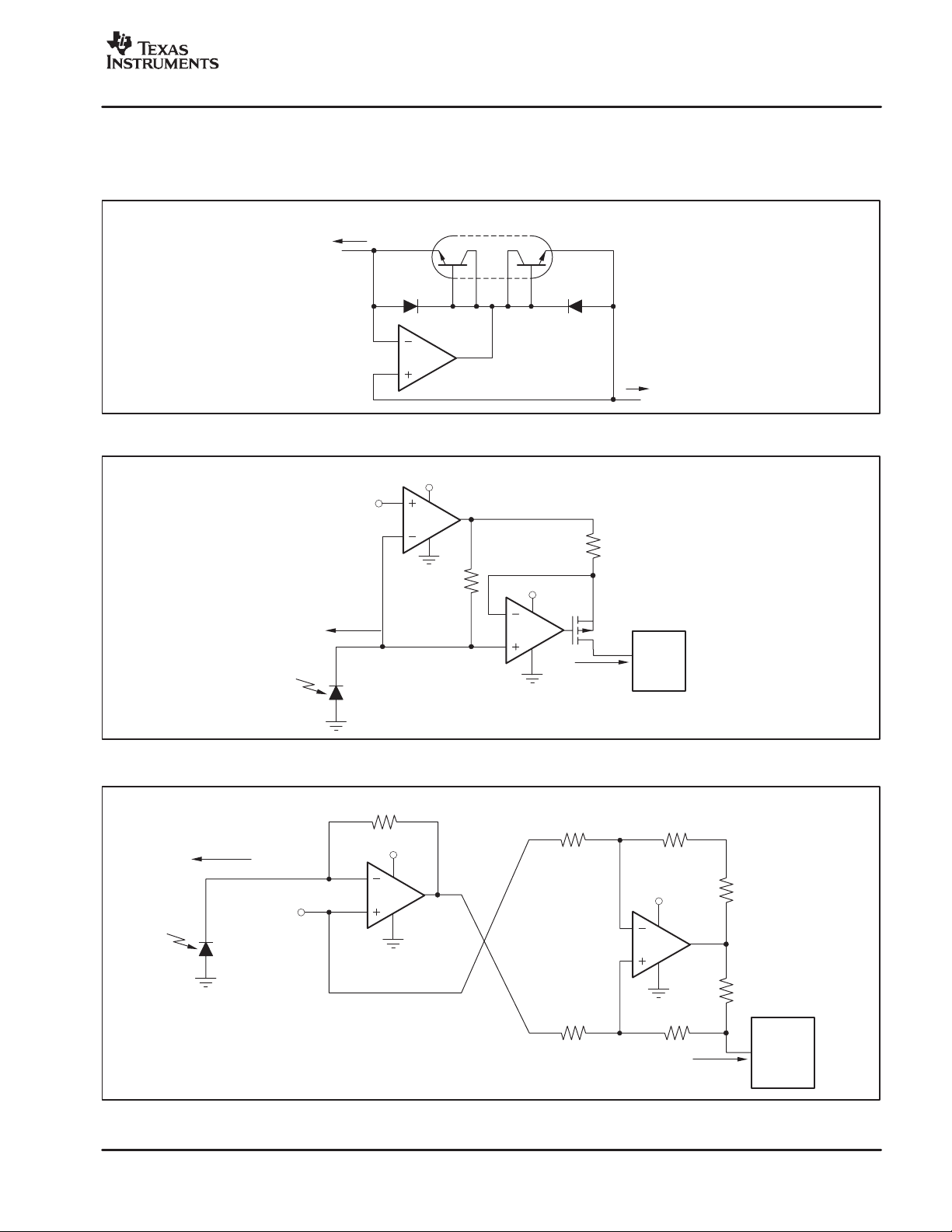
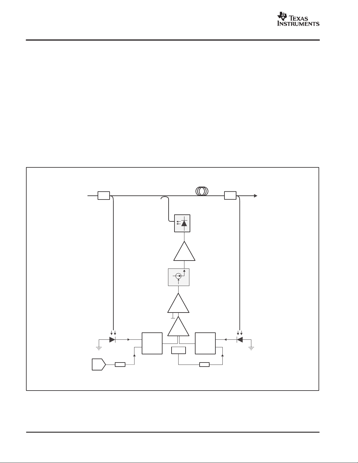
ERBIUM-DOPED FIBER OPTIC AMPLIFIER
(EDFA)
The LOG114 was designed for optical networking systems. Figure 13 shows a block diagram of the LOG114
in a typical EDFA application. This application uses t wo
log amps to measure the optical input and output power
of the amplifier. A difference amplifier subtracts the log
output signals of both log amps and applies an error
voltage to the proportional-integral-derivative (PID)
controller. The controller output adjusts a voltage-controlled current source (V
), which then drives the pow-
CCS
er op amp and pump laser. The desired optical gain is
achieved when the error voltage at the PID is zero.
The log ratio function is the optical power gain of the
EDFA. This circuitry forms an automatic power level
control loop.
Tap
1%
An alternate design of the system shown in Figure 13
is possible because the LOG114 inherently takes the
log ratio. Therefore, one log amp can be eliminated by
connecting one of the photodiodes to the LOG114 I
input, and the other to the I
input. The differential
2
amplifier would then be eliminated.
The LOG114 is uniquely suited for most EDFA
applications because of its fast rise and fall times
(typically less than 1µs for a 100:1 current input step).
It also measures a very wide dynamic range of up to
eight decades.
Tap
Fiber
1%
1
DAC
PumpLaser
Power
V
V
ERROR
OUT2
Op Amp
V
CCS
LOG114LOG114
I
2
I
REF2
R
REF2
OPA569
I
L
PID
I
1
I
REF1
R
REF1
V
Diff
OUT1
REF
Figure 13. Erbium-Doped Fiber Optic Amplifier (EDFA) block diagram.
20
Page 21

www.ti.com
"#$$%
SBOS301A − M AY 2004 − REVISED MARCH 2007
INSIDE THE LOG114
The LOG114 uses two matched logarithmic amplifiers
and A2 with logging diodes in the feedback loops) to
(A
1
generate the outputs log (I1) and log (I2), respectively.
The gain of 6.25 differential amplifier (A3) subtracts the
output of A2 from the output of A1, resulting in [log (I1)
− log (I2)], or log (I1/I2). The symmetrical design of the
A1 and A2 logarithmic amps allows I1 and I2 to be used
interchangeably, and provides good bandwidth and
phase characteristics with frequency.
DEFINITION OF TERMS
Transfer Function
The ideal transfer function of the LOG114 is:
I
1
ǒ
V
This transfer function can be seen graphically in the typical characteristic curve, V
When a pedestal, or offset, voltage (V
to the Com pin, an additional offset term is introduced
into the equation:
V
Accuracy
Accuracy considerations for a log ratio amplifier are
somewhat more complicated than for other amplifiers.
This complexity exists because the transfer function is
nonlinear and has two inputs, each of which can vary
over a wide
dynamic range. The accuracy for any combination of
inputs is determined from the total error specification.
Total Error
The total error is the deviation of the actual output from
the ideal output. Thus,
It represents the sum of all the individual components
of error normally associated with the log amp when operating in the current input mode. The worst-case error
for any given ratio of I1/I2 is the largest of the two errors
when I1 and I2 are considered separately . Temperature
can also affect total error.
Errors RTO and RTI
As with any transfer function, errors generated by the
function may be Referred-to-Output (RTO) or Referredto-Input (RTI). In this respect, log amps have a unique
property: given some error voltage at the log amp output, that error corresponds to a constant percent of the
input, regardless of the actual input level.
+ 0.375 log
LOGOUT
+ 0.375 log
LOGOUT
V
LOGOUT(ACTUAL)
Ǔ
1
2
LOGOUT
I
1
ǒ
Ǔ
1
2
= V
LOGOUT(IDEAL)
) V
vs I
REF
Com
Com
± Total Error
(17)
.
) is connected
(18)
Log Conformity
For the LOG114, log conformity is calculated in the
same way as linearity and is plotted as I1/I2 on a semilog scale. In many applications, log conformity is the
most important specification. This condition is true because bias current errors are negligible (5pA for the
LOG114), and the scale factor and offset errors may be
trimmed to zero or removed by system calibration.
These factors leave log conformity as the major source
of error.
Log conformity is defined as the peak deviation from the
best fit straight line of the V
curve. Log conformity is then expressed as a percent of
ideal full−scale output. Thus, the nonlinearity error expressed in volts over m decades is:
V
LOGOUT (NONLIN)
where N is the log conformity error, in percent.
INDIVIDUAL ERROR COMPONENTS
The ideal transfer function with current input is:
V
The actual transfer function with the major components
of error is:
0.375(1 " DK) log
where:
To determine the typical error resulting from these error
components, first compute the ideal output. Then calculate the output again, this time including the individual
error components. Then determine the error in percent
using Equation (21):
IDEAL
LOGOUT
∆K = gain error (0.4%, typ, as specified in the Electri-
cal Characteristics table)
IB1 = bias current of A1 (5pA, typ)
IB2 = bias current of A2 (5pA, typ)
m = number of decades over which the log
conformity error is specified
N = log conformity error (0.1%, typ for m = 5 decades;
0.9% typ for m = 7.5 decades)
V
= output of fset voltage (11mV , typ for ±5V sup-
OSO
plies; 14mV, typ for +5V supplies)
Ť
%error +
= 0.375V/decade • 2Nm
+ 0.375 log
ǒ
V
LOGOUT
IDEAL
V
LOGOUTIDEAL
LOGOUT
I
ǒ
1
I
1
Ǔ
" 2Nm " V
I
2
*V
LOGOUT
versus log (I1/I2)
1
Ǔ
2
OSO
Ť
TYP
100%
(19)
(20)
(21)
21
Page 22

"#$$%
SBOS301A − M AY 2004 − REVISED MARCH 2007
www.ti.com
For example, in a system configured for measurement
of five decades, with I
V
LOGOUT
V
LOGOUT
+ 0.375 log
IDEAL
+ 0.375(1 " 0.004) log
TYP
" 2(0.001)(5)" 0.011
= 1mA, and I2 = 10µA:
1
*3
10
ǒ
Ǔ
+ 0.75V
*5
10
10−3*5 10
ǒ
10−5*5 10
−12
−12
(22)
Ǔ
(23)
Using the positive error components (+∆K, +2Nm, and
+V
) to calculate the maximum typical output:
OSO
V
LOGOUT
+ 0.774V
TYP
(24)
Therefore, the error in percent is:
%error +
|
0.75*0.774
0.75
|
100% + 3.2%
(25)
QFN PACKAGE
The LOG114 comes in a QFN-16 package. This leadless package has lead contacts on all four sides of the
bottom of the package, thereby maximizing board
space. An exposed leadframe die pad on the bottom of
the package enhances thermal and electrical characteristics.
QFN packages are physically small, have a smaller
routing area, improved thermal performance, and improved electrical parasitics. Additionally , t h e a bsence of
external leads eliminates bent-lead issues.
The QFN package can be easily mounted using standard printed circuit board (PCB) assembly techniques.
See Application Note QFN/SON PCB Attachment
(SLUA271) and Application Report Quad Flatpack No−
Lead Logic Packages (SCBA017), both available for
download at www.ti.com.
The exposed leadframe die pad on the bottom of
the package should be connected to V−.
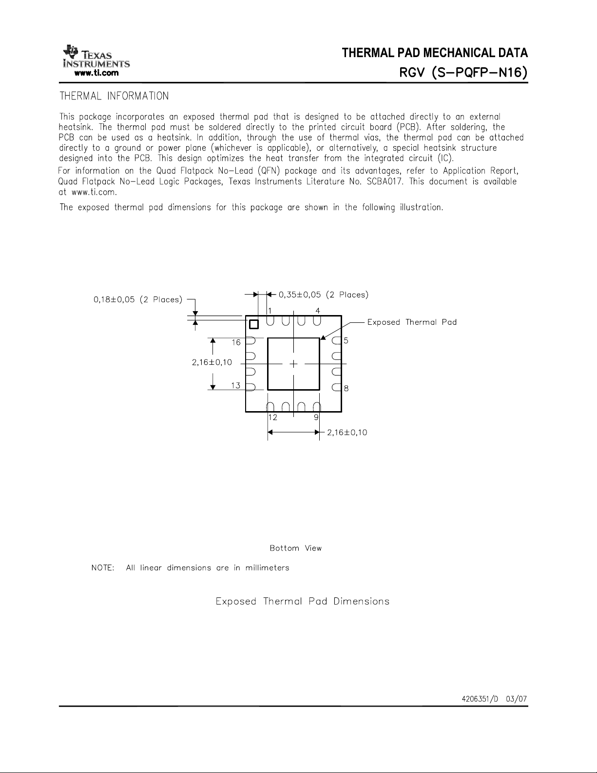
QFN LAYOUT GUIDELINES
The exposed leadframe die pad on the QFN package
should be soldered to a thermal pad on the PCB. A mechanical drawing showing an example layout is attached at the end of this data sheet. Refinements to this
layout may be necessary based on assembly process
requirements. Mechanical drawings located at the end
of this data sheet list the physical dimensions for the
package and pad. The five holes in the landing pattern
are optional, and are intended for use with thermal vias
that connect the leadframe die pad to the heatsink area
on the PCB.
Soldering the exposed pad significantly improves
board-level reliability during temperature cycling, key
push, package shear, and similar board-level tests.
Even with applications that have low-power dissipation,
the exposed pad must be soldered to the PCB to provide structural integrity and long-term reliability.
22
Page 23

PACKAGE OPTION ADDENDUM
www.ti.com
29-Mar-2007
PACKAGING INFORMATION
Orderable Device Status
(1)
Package
Type
Package
Drawing
Pins Package
Qty
Eco Plan
LOG114AIRGVR ACTIVE QFN RGV 16 2500 Green (RoHS &
no Sb/Br)
LOG114AIRGVT ACTIVE QFN RGV 16 250 Green (RoHS &
no Sb/Br)
(1)
The marketing status values are defined as follows:
ACTIVE: Product device recommended for new designs.
LIFEBUY: TI has announced that the device will be discontinued, and a lifetime-buy period is in effect.
NRND: Not recommended for new designs. Device is in production to support existing customers, but TI does not recommend using this part in
a new design.
PREVIEW: Device has been announced but is not in production. Samples may or may not be available.
OBSOLETE: TI has discontinued the production of the device.
(2)
Eco Plan - The planned eco-friendly classification: Pb-Free (RoHS), Pb-Free (RoHS Exempt), or Green (RoHS & no Sb/Br) - please check
http://www.ti.com/productcontent for the latest availability information and additional product content details.
TBD: The Pb-Free/Green conversion plan has not been defined.
Pb-Free (RoHS): TI's terms "Lead-Free" or "Pb-Free" mean semiconductor products that are compatible with the current RoHS requirements
for all 6 substances, including the requirement that lead not exceed 0.1% by weight in homogeneous materials. Where designed to be soldered
at high temperatures, TI Pb-Free products are suitable for use in specified lead-free processes.
Pb-Free (RoHS Exempt): This component has a RoHS exemption for either 1) lead-based flip-chip solder bumps used between the die and
package, or 2) lead-based die adhesive used between the die and leadframe. The component is otherwise considered Pb-Free (RoHS
compatible) as defined above.
Green (RoHS & no Sb/Br): TI defines "Green" to mean Pb-Free (RoHS compatible), and free of Bromine (Br) and Antimony (Sb) based flame
retardants (Br or Sb do not exceed 0.1% by weight in homogeneous material)
(2)
Lead/Ball Finish MSL Peak Temp
CU NIPDAU Level-2-260C-1 YEAR
CU NIPDAU Level-2-260C-1 YEAR
(3)
(3)
MSL, Peak Temp. -- The Moisture Sensitivity Level rating according to the JEDEC industry standard classifications, and peak solder
temperature.
Important Information and Disclaimer:The information provided on this page represents TI's knowledge and belief as of the date that it is
provided. TI bases its knowledge and belief on information provided by third parties, and makes no representation or warranty as to the
accuracy of such information. Efforts are underway to better integrate information from third parties. TI has taken and continues to take
reasonable steps to provide representative and accurate information but may not have conducted destructive testing or chemical analysis on
incoming materials and chemicals. TI and TI suppliers consider certain information to be proprietary, and thus CAS numbers and other limited
information may not be available for release.
In no event shall TI's liability arising out of such information exceed the total purchase price of the TI part(s) at issue in this document sold by TI
to Customer on an annual basis.
Addendum-Page 1
Page 24
Page 25
Page 26

Page 27

IMPORTANT NOTICE
Texas Instruments Incorporated and its subsidiaries (TI) reserve the right to make corrections, modifications,
enhancements, improvements, and other changes to its products and services at any time and to
discontinue any product or service without notice. Customers should obtain the latest relevant information
before placing orders and should verify that such information is current and complete. All products are sold
subject to TI’s terms and conditions of sale supplied at the time of order acknowledgment.
TI warrants performance of its hardware products to the specifications applicable at the time of sale in
accordance with TI’s standard warranty. Testing and other quality control techniques are used to the extent
TI deems necessary to support this warranty. Except where mandated by government requirements, testing
of all parameters of each product is not necessarily performed.
TI assumes no liability for applications assistance or customer product design. Customers are responsible
for their products and applications using TI components. To minimize the risks associated with customer
products and applications, customers should provide adequate design and operating safeguards.
TI does not warrant or represent that any license, either express or implied, is granted under any TI patent
right, copyright, mask work right, or other TI intellectual property right relating to any combination, machine,
or process in which TI products or services are used. Information published by TI regarding third-party
products or services does not constitute a license from TI to use such products or services or a warranty or
endorsement thereof. Use of such information may require a license from a third party under the patents or
other intellectual property of the third party, or a license from TI under the patents or other intellectual
property of TI.
Reproduction of information in TI data books or data sheets is permissible only if reproduction is without
alteration and is accompanied by all associated warranties, conditions, limitations, and notices.
Reproduction of this information with alteration is an unfair and deceptive business practice. TI is not
responsible or liable for such altered documentation.
Resale of TI products or services with statements different from or beyond the parameters stated by TI for
that product or service voids all express and any implied warranties for the associated TI product or service
and is an unfair and deceptive business practice. TI is not responsible or liable for any such statements.
Following are URLs where you can obtain information on other Texas Instruments products and application
solutions:
Products
Applications
Amplifiers amplifier.ti.com Audio www.ti.com/audio
Data Converters dataconverter.ti.com Automotive www.ti.com/automotive
DSP dsp.ti.com Broadband www.ti.com/broadband
Interface interface.ti.com Digital Control www.ti.com/digitalcontrol
Logic logic.ti.com Military www.ti.com/military
Power Mgmt power.ti.com Optical Networking www.ti.com/opticalnetwork
Microcontrollers microcontroller.ti.com Security www.ti.com/security
Low Power Wireless www.ti.com/lpw Telephony www.ti.com/telephony
Video & Imaging www.ti.com/video
Wireless www.ti.com/wireless
Mailing Address: Texas Instruments
Post Office Box 655303 Dallas, Texas 75265
Copyright © 2007, Texas Instruments Incorporated
 Loading...