

Page 1

User's Guide
SNAU219–June 2017
LMX2595 EVM Instructions – 19-GHz Wideband Low Noise
PLL With Integrated VCO
This Evaluation Module is for the LMX2595, which is the first PLL with integrated VCO in industry to get
fundamental VCO output up to 15 GHz. The industry leading PLL FOM is -236 dBc/Hz with 1/f of -129
dBc/Hz. This device supports JESD204B standard (it can generate or repeat the SYSREF signal) which
makes it ideal to clock high speed data converters. The integrated jitter from the EVM measurements is
less than 50 fs at 9 GHz carrier frequency. By providing a SYNC signal, the user can synchronize the
output phase across multiple LMX2595 devices. LMX2595 can also generate a frequency ramp which can
be demonstrated in this evaluation module. With an on-board oscillator, setup process only requires a
3.3V power supply and an included Reference Pro module (For SPI Programming interface). The software
is simple, with an intuitive and user friendly GUI.
1 Evaluation Board Setup .................................................................................................... 3
2 EVM Description ............................................................................................................. 4
3 Bringing LMX2595 to a Lock State ........................................................................................ 8
4 Current Loop Filter Configuration ........................................................................................ 10
5 Key Results to Expect ..................................................................................................... 11
Appendix A Schematic .......................................................................................................... 12
Appendix B Bill of Materials .................................................................................................... 13
Appendix C Board Layers Stack-Up........................................................................................... 15
Appendix D Changing Reference Oscillator and Setup..................................................................... 16
Appendix E Connecting Reference Pro....................................................................................... 18
Appendix F Ramping Feature ................................................................................................. 21
Appendix G SYSREF Feature ................................................................................................. 23
SNAU219–June 2017
Submit Documentation Feedback
Figure 1. LMX2595EVM
Contents
LMX2595 EVM Instructions – 19-GHz Wideband Low Noise PLL With
Copyright © 2017, Texas Instruments Incorporated
Integrated VCO
1
Page 2

Appendix H VCO Calibration ................................................................................................... 28
Appendix I Enabling Onboard DC-DC Buck Converter (TPS62150)..................................................... 30
Appendix J Appendix J: Using the VCO Doubler ........................................................................... 31
Trademarks
All trademarks are the property of their respective owners.
www.ti.com
2
LMX2595 EVM Instructions – 19-GHz Wideband Low Noise PLL With
Integrated VCO
Copyright © 2017, Texas Instruments Incorporated
Submit Documentation Feedback
SNAU219–June 2017
Page 3

3.3 Volt supply
LMX2594
Output to
analyzer
Serial Interface
Reference
Pro
LMX2595EVM
USB Æ PC
Reference XO
If unused,
terminate
(50ohm)
www.ti.com
1 Evaluation Board Setup
Evaluation Board Setup
Figure 2. LMX2595EVM Setup
SPACER
1. Power:
(a) Set power supply to 3.3 V with 600-mA current limit and connect to VCCSMA.
2. Input Signal:
(a) VC-708 100-MHz on-board oscillator enabled (default). To use another reference, see Appendix D.
3. Programming Interface:
• Reference Pro will provide SPI interface to program LMX2595:
(a) Connect USB cable from laptop or PC to USB port in Reference Pro. This provides power to
Reference Pro Board and communication with TICS GUI
(b) Connect 10 pin ribbon cable from Reference Pro to LMX2595EVM as shown above.
4. Output:
(a) Connect RFoutAM or RFoutAP to a phase noise Analyzer. Connect a 50-Ω on the unused output if
you are using only single-ended. Use a balun if you are using differential.
SNAU219–June 2017
Submit Documentation Feedback
Copyright © 2017, Texas Instruments Incorporated
LMX2595 EVM Instructions – 19-GHz Wideband Low Noise PLL With
Integrated VCO
3
Page 4

Power supply.
3.3 Volt
Voltage regulator
not enabled
Diff. RF output A
Diff. RF output B
100 MHz XO
Diff. reference input
Single ended signal
can be used.
Lock indicator LED
Switch to select:
1) SPI Read back
2) Lock indicator
(1 OR 2)
LMX2595
Serial interface
Loop filter components
(*_LF)
123456789
10
Serial interface pin out
Sync
SysRef
EVM Description
2 EVM Description
The LMX2595 is populated on a 4-layer PCB. This brief description should help you use the EVM:
www.ti.com
The serial interface pin description is as follow:
4
LMX2595 EVM Instructions – 19-GHz Wideband Low Noise PLL With
Integrated VCO
Table 1. EVM and Serial Interface Connector
Figure 3. LMX2595EVM Description
Description
NO. NAME
1
2 CSB
3 MUXout
4 SDI
5 Not Used
6 GND
7 RampCLK
8 SCK
9 SysRefReq
10 SYNC
RAMPDIR and CE (Choose with
Resistors on Board)
Copyright © 2017, Texas Instruments Incorporated
SNAU219–June 2017
Submit Documentation Feedback
Page 5
www.ti.com
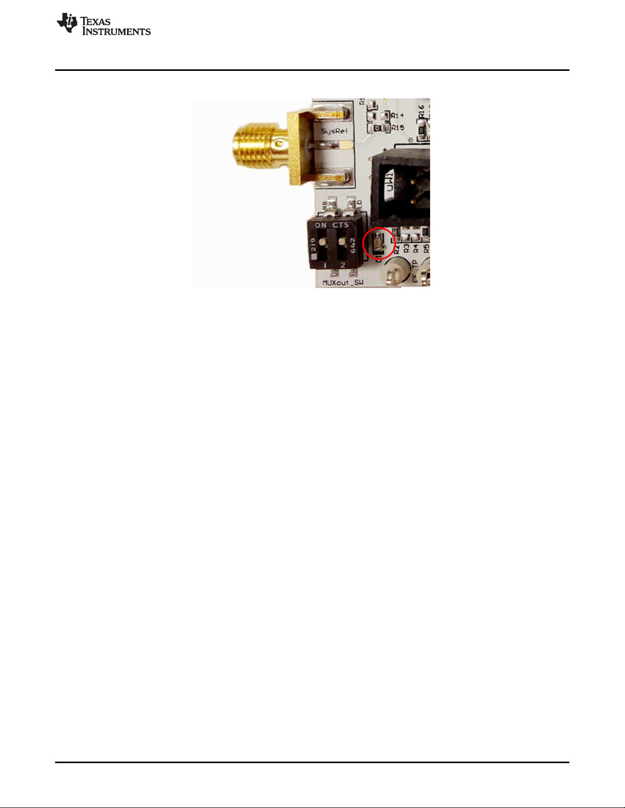
The LD switch must be on to enable Lock indicator:
EVM Description
Figure 4. LD Lock Detect
SNAU219–June 2017
Submit Documentation Feedback
LMX2595 EVM Instructions – 19-GHz Wideband Low Noise PLL With
Copyright © 2017, Texas Instruments Incorporated
Integrated VCO
5
Page 6

EVM Description
2.1 Installing the Software
1. Download TICS Pro from the TI Website at www.ti.com/tool/TICSPRO-SW
2. Install it by following the wizard
3. Search for LMX2595: Click on Select Device From menu bar →PLL+VCO→LMX2595
www.ti.com
Figure 5. Search for LMX2595 on TICS Pro
4. You are now ready to use this software. Verify that you can communicate with Reference Pro. Select
interface under USB communications:
Figure 6. USB Communications on TICS Pro
6
LMX2595 EVM Instructions – 19-GHz Wideband Low Noise PLL With
Integrated VCO
Copyright © 2017, Texas Instruments Incorporated
Submit Documentation Feedback
SNAU219–June 2017
Page 7

www.ti.com
5. Click on identify and you will see the LED (MSP430 Supplied) Blink on Reference Pro
EVM Description
Figure 7. USB Communication Between TICS Pro and Reference Pro
SNAU219–June 2017
Submit Documentation Feedback
LMX2595 EVM Instructions – 19-GHz Wideband Low Noise PLL With
Copyright © 2017, Texas Instruments Incorporated
Integrated VCO
7
Page 8
Bringing LMX2595 to a Lock State
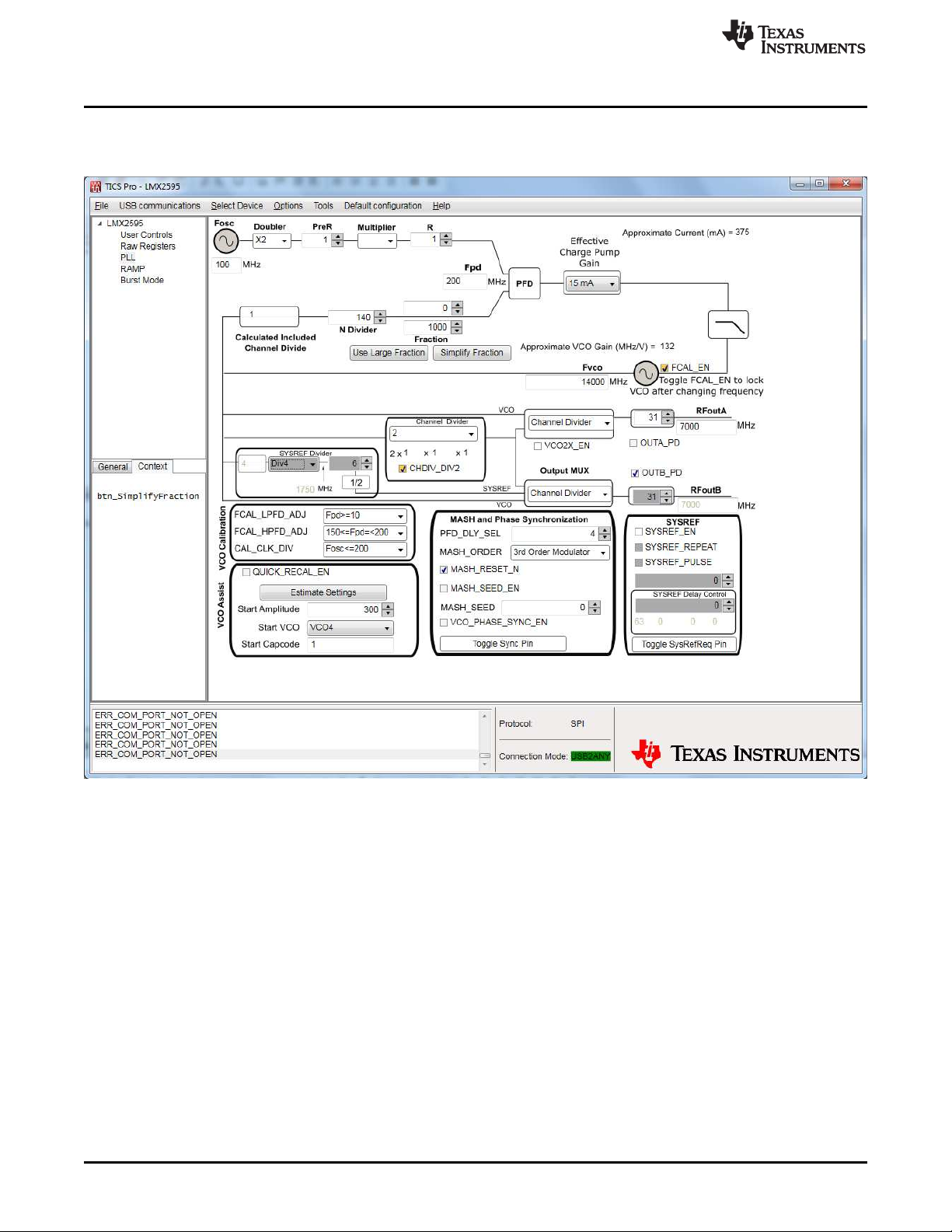
3 Bringing LMX2595 to a Lock State
Load the default mode by selecting it as shown in Figure 8:
www.ti.com
Figure 8. TICS Pro GUI LMX2595 Default Configuration
8
LMX2595 EVM Instructions – 19-GHz Wideband Low Noise PLL With
Integrated VCO
Copyright © 2017, Texas Instruments Incorporated
Submit Documentation Feedback
SNAU219–June 2017
Page 9
www.ti.com
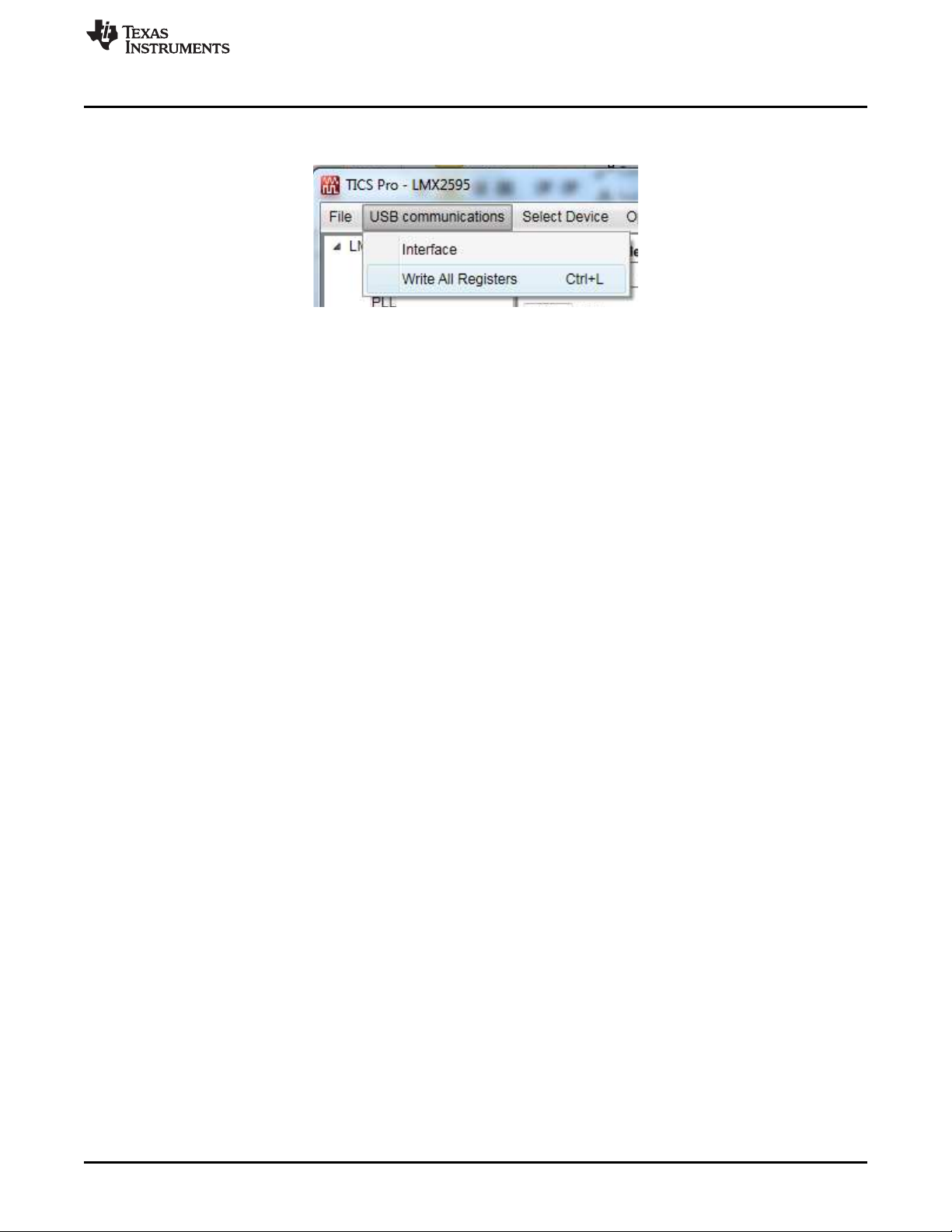
For best results, in the User Controls Tab in TICS Pro. Under General Controls, check and uncheck the
Reset box. After the reset, Write all registers as shown in Figure 9:
Bringing LMX2595 to a Lock State
Figure 9. TICS Pro Write All Registers
SNAU219–June 2017
Submit Documentation Feedback
LMX2595 EVM Instructions – 19-GHz Wideband Low Noise PLL With
Copyright © 2017, Texas Instruments Incorporated
Integrated VCO
9
Page 10

Current Loop Filter Configuration
4 Current Loop Filter Configuration
The parameters for the loop filters are:
Table 2. Current Loop Filter Configuration
PARAMETER VALUE
VCO Gain 132 MHz/V
Loop Bandwidth 285 kHz
Phase Margin 65 deg
C1_LF 390 pF
C2_LF 68 nF
C3_LF Open
C4_LF 1800 pF
R2 68 Ω
R3_LF 0 Ω
R4_LF 18 Ω
Effective Charge Pump Gain 15 mA
Phase Detector Frequency (MHz) 200 MHz
VCO Frequency
www.ti.com
Designed for 15 GHz, but works
over the whole frequency range
10
Figure 10. Current Loop Filter Configuration
For detailed design and simulation, see the PLLatinum Sim Tool.
For application notes, blogs,or videos on our products, see http://www.ti.com/pll.
LMX2595 EVM Instructions – 19-GHz Wideband Low Noise PLL With
Integrated VCO
Copyright © 2017, Texas Instruments Incorporated
Submit Documentation Feedback
SNAU219–June 2017
Page 11

www.ti.com
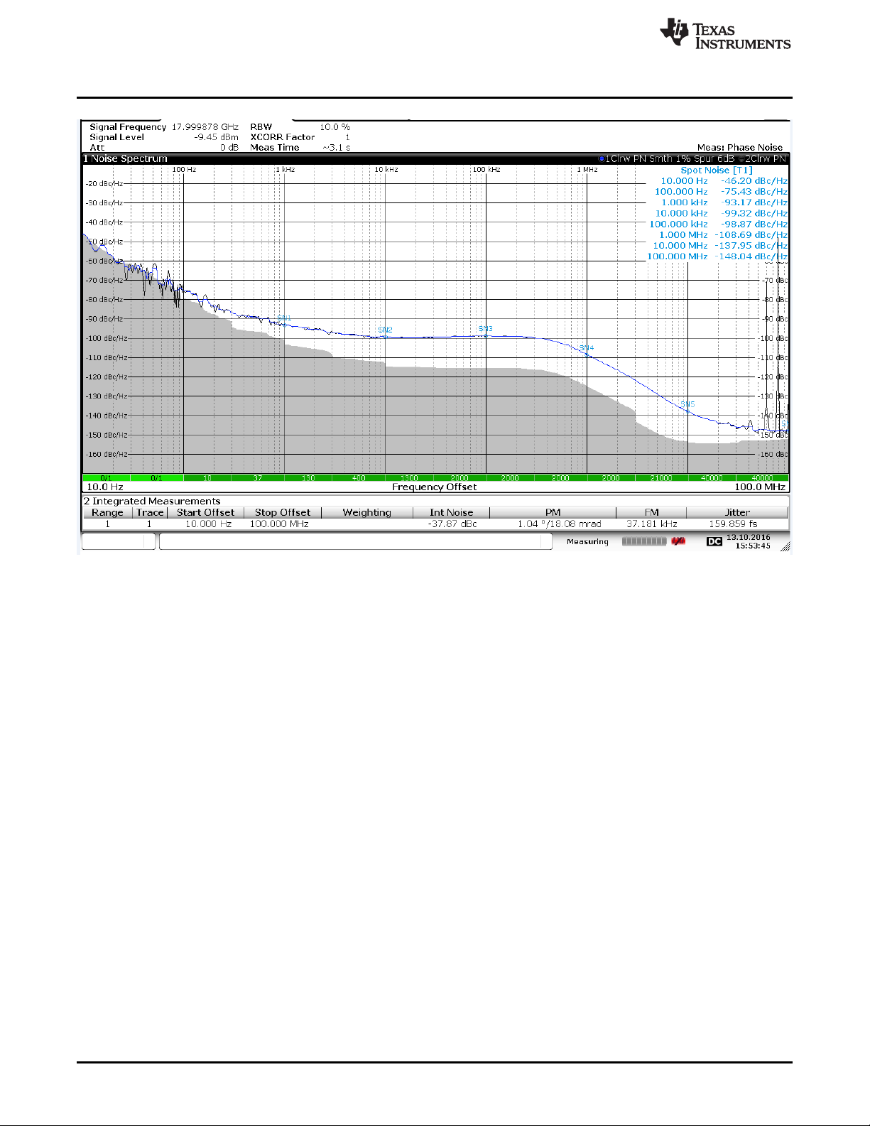
5 Key Results to Expect
Key Results to Expect
This assumes that the input reference is very clean, such as a 100-MHz Wenzel oscillator. A signal
generator is NOT sufficiently clean. The LMX2595 requires an external reference.
SNAU219–June 2017
Submit Documentation Feedback
Figure 11. Phase Noise Plot at 14-GHz Output Frequency
LMX2595 EVM Instructions – 19-GHz Wideband Low Noise PLL With
Copyright © 2017, Texas Instruments Incorporated
Integrated VCO
11
Page 12

Appendix A
SNAU219–June 2017
Schematic
12
Schematic
Figure 12. Schematic
Copyright © 2017, Texas Instruments Incorporated
Submit Documentation Feedback
SNAU219–June 2017
Page 13

Appendix B
SNAU219–June 2017
Bill of Materials
Table 3. Bill of Materials
DESIGNATOR DESCRIPTION MANUFACTURER PART NUMBER QUANTITY
!PCB Printed-Circuit Board Any SV601308 1
C1, C3, C9, C14,
C15, C17, C30
C1_LF
C2, C4, C8, C16
C2_LF
C4_LF
C5, C6, C7, C10,
C11, C12
C13, C18, C23,
C24, C26, C27,
C28, C29
C19, C20, C21,
C22, C25
CE_TP, CSB_TP,
GND_TP,
MUXout_TP,
RampCLK_TP,
RampDIR_TP,
SCK_TP, SDI_TP,
SYNC_TP,
SysRefReq_TP,
Vcc_TP,
VccRF_TP,
Vtune_TP
Cin_0
Cout0
Css
D1 LED, Green, SMD Lite-On LTST-C190GKT 1
L1, L2
L1_TPS
LBL1
MUXout_SW
CAP, CERM, 0.1 µF, 16 V, ±5%,
CAP, CERM, 0.068 µF, 50 V,
CAP, CERM, 1800 pF, 50 V,
CAP, CERM, 0.01 µF, 16 V,
CAP, CERM, 1 µF, 16 V, ±10%,
Test Point, Compact, White, TH Keystone 5007 13
CAP, CERM, 3300 pF, 50 V,
Inductor, Multilayer, Air Core, 18
Inductor, Shielded, Composite,
Labels, 0.650" W x 0.200" H -
Switch, SPST, Slide, Off-On, 2
X7R, 0603
CAP, CERM, 390 pF, 50 V,
±5%, C0G/NP0, 0603
CAP, CERM, 10 µF, 10 V,
±10%, X5R, 0805
±10%, X7R, 0603
±5%, C0G/NP0, 0603
±10%, X7R, 0402
X7R, 0603
CAP, CERM, 10 µF, 10 V,
±20%, X5R, 0603
CAP, CERM, 10 µF, 25 V,
±10%, X5R, 0805
CAP, CERM, 22 µF, 16 V,
±10%, X5R, 0805
±5%, C0G/NP0, 0603
nH, 0.3 A, 0.36 Ω, SMD
2.2 µH, 3.7 A, 0.02 Ω, SMD
Thermal Transfer Printable
10,000 per roll
Pos, 0.1 A, 20 V, SMD
CTS Electrocomponents 219-2MST 1
AVX 0603YC104JAT2A 7
Kemet C0603C391J5GACTU 1
Kemet C0805C106K8PACTU 4
MuRata GRM188R71H683KA93D 1
MuRata GRM1885C1H182JA01D 1
AT Ceramics 520L103KT16T 6
TDK C1608X7R1C105K080AC 8
TDK C1608X5R1A106M080AC 5
MuRata GRM219R61E106KA12D 1
TDK C2012X5R1C226K125AC 1
MuRata GRM1885C1H332JA01D 1
MuRata LQG15HS18NJ02D 2
Coilcraft XFL4020-222MEB 1
Brady THT-14-423-10 1
SNAU219–June 2017
Submit Documentation Feedback
Copyright © 2017, Texas Instruments Incorporated
Bill of Materials
13
Page 14

Appendix B
OSCinM, OSCinP,
R3_LF, R12, R15,
R24b, R26, R29b,
FID5, FID6, FID10,
R3, R4, R6, R10,
R29, Rtps1, Rtps2
www.ti.com
Table 3. Bill of Materials (continued)
DESIGNATOR DESCRIPTION MANUFACTURER PART NUMBER QUANTITY
SYNC, SysRef,
Vcc
R1 RES, 330 Ω, 5%, 0.1 W, 0603 Yageo America RC0603JR-07330RL 1
R2 RES, 100 k, 5%, 0.1 W, 0603 Vishay-Dale CRCW0603100KJNEA 1
R2_LF RES, 68, 5%, 0.1 W, 0603 Vishay-Dale CRCW060368R0JNEA 1
R31, R34, R35,
R36, R41, R42,
R43, R44, R45
R4_LF RES, 18, 5%, 0.1 W, 0603 Vishay-Dale CRCW060318R0JNEA 1
R5, R7, R8, R9,
R16, R19, R20,
R22
R33 RES, 10 Ω, 5%, 0.1 W, 0603 Vishay-Dale CRCW060310R0JNEA 1
R32 RES, 100, 1%, 0.1 W, 0603 Vishay-Dale CRCW0603100RFKEA 1
R37, R38, R39,
R40
Rfbb1 RES, 180 k, 0.1%, 0.1 W, 0603 Yageo America RT0603BRD07180KL 1
Rfbt1 RES, 562 k, 1%, 0.1 W, 0603 Vishay-Dale CRCW0603562KFKEA 1
RFoutAM,
RFoutAP,
RFoutBM,
RFoutBP
U1
U3
uWire
Y1
C3_LF
FID11
PinControl
R17, R18, R21,
R23
R11, R14, R24,
R13 RES, 100, 5%, 0.1 W, 0603 Vishay-Dale CRCW0603100RJNEA 0
R25, R30 RES, 51, 5%, 0.1 W, 0603 Vishay-Dale CRCW060351R0JNEA 0
R27, R28 RES, 140, 1%, 0.1 W, 0603 Vishay-Dale CRCW0603140RFKEA 0
Rtps RES, 0, 5%, 0.125 W, 0805 Vishay-Dale CRCW08050000Z0EA 0
Connector, SMT, End launch
SMA 50 ohm
RES, 0, 5%, 0.1 W, 0603 Vishay-Dale CRCW06030000Z0EA 15
RES, 12 kΩ, 5%, 0.1 W, 0603 Vishay-Dale CRCW060312K0JNEA 8
RES, 50, 0.1%, 0.05 W, 0402 Vishay-Dale FC0402E50R0BST1 4
JACK, SMA, 50 Ω, Gold, Edge
Mount
High Performance, Wideband
PLLatinum RF Synthesizer,
RHA0040A (VQFN-40)
Buck Step-Down Regulator with
3 to 17 V Input and 0.9 to 6 V
Output, –40 to 85°C, 16-Pin
QFN (RGT), Green (RoHS and
no Sb/Br)
Header (shrouded), 100 mil,
5x2, Gold plated, SMD
Crystal Oscillator, 100 MHz,
LVDS, 3.3V, SMD
CAP, CERM, 300 pF, 100 V,
±5%, C0G/NP0, 0603
Fiducial mark. There is nothing
to buy or mount.
Header, 100 mil, 4x2, Gold,
SMT
RES, 12 kΩ, 5%, 0.1 W, 0603 Vishay-Dale CRCW060312K0JNEA 0
RES, 0, 5%, 0.1 W, 0603, RES,
0, 5%, 0.1 W, 0603, RES, 0,
5%, 0.1 W, 0603, RES, 0, 5%,
0.1 W, 0603, RES, 0 Ω, 5%,
0.1W, 0603, RES, 0 Ω, 5%, 0.1
W, 0603
Emerson Network Power
Connectivity
Johnson 142-0771-831 4
Texas Instruments LMX2595RHAR 1
Texas Instruments TPS62150RGTR 0
FCI 52601-S10-8LF 1
Vectron
MuRata GRM1885C2A301JA01D 0
N/A N/A 0
Molex 0015910080 0
Vishay-Dale CRCW06030000Z0EA 0
142-0701-851 5
VC-708-EDE-FNXN-
100M000000
1
14
Bill of Materials
Copyright © 2017, Texas Instruments Incorporated
Submit Documentation Feedback
SNAU219–June 2017
Page 15

Total Board thickness is 62 mils.
Appendix C
SNAU219–June 2017
Board Layers Stack-Up
SNAU219–June 2017
Submit Documentation Feedback
Figure 13. Board Layer Stack-Up
Copyright © 2017, Texas Instruments Incorporated
Board Layers Stack-Up
15
Page 16
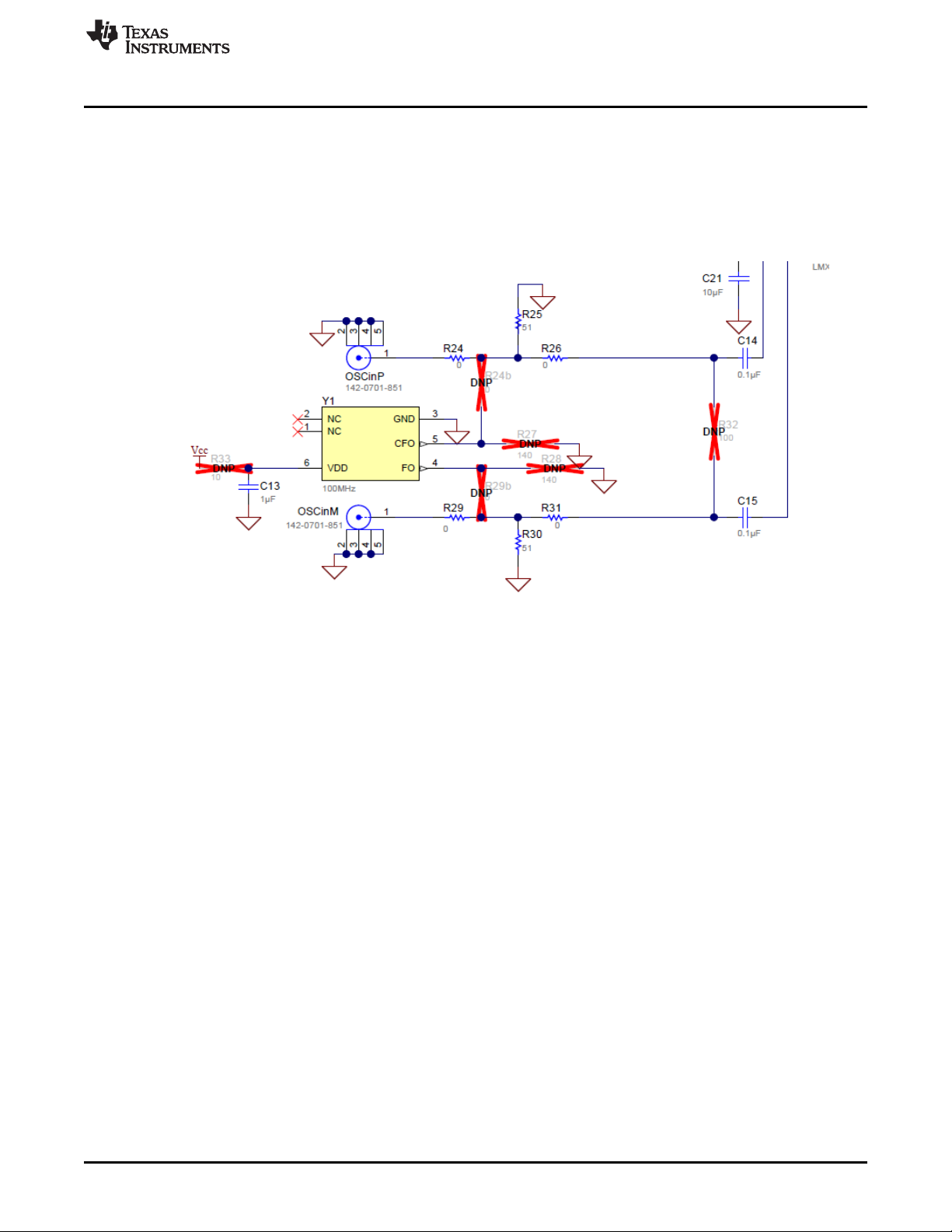
Appendix D
SNAU219–June 2017
Changing Reference Oscillator and Setup
The reference can be single-ended or differential. To measure the performance of the PLL ONLY,
the reference must have at least this level of performance. We understand that this can be a
challenge at 100-Hz offset:
Table 4. Reference Oscillator Requirements
100-MHz REFERENCE MINIMUM REQUIREMENTS FOR A 0.4-dB IMPACT ON PLL INBAND PN
Offset [Hz] 100 1k 10k 100k
Noise level [
dBc/Hz]
(1)
A noise source 10 dB down from the PLL noise will contribute to raise the noise by 0.4 dB.
–139 –149 –159 –164
There are different options to provide a reference oscillator to LMX2595: Use on-board oscillator (default),
Enable LMK61xx from Reference Pro PCB, use external oscillator.
By default the onboard oscillator is enabled. To use external reference, onboard oscillator must be
disabled. Having multiple 100 MHz enabled or powered sharing VCCor Gnd will degrade the phase noise
performance of LMX2595.
For differential pair connection:
1. Switch R24b to R24.
2. Switch R29b to R29
3. Must remove R33 to remove power from oscillator
(1)
16
Figure 14. Single-Ended Reference Configuration
Changing Reference Oscillator and Setup
Copyright © 2017, Texas Instruments Incorporated
Submit Documentation Feedback
SNAU219–June 2017
Page 17
www.ti.com
For single-ended:
1. Switch R24b to R24.
2. Switch R29b to R29
3. Must remove R33 to remove power from oscillator
4. Populate R25 and R30.
5. Remove R32
Appendix D
Figure 15. Differential Reference Configuration
SNAU219–June 2017
Submit Documentation Feedback
Copyright © 2017, Texas Instruments Incorporated
Changing Reference Oscillator and Setup
17
Page 18
3.3 Volt supply
LMX2594
Output to
analyzer
Serial Interface
Reference Pro
LMX2595EVM
USB Æ PC
On-board Crystal
should be disabled
If unused,
terminate
(50ohm)
LMK61PD0A2
Reference
LMK61PD0A2 Output
LMX2594 OSCINM &
OSCINP input
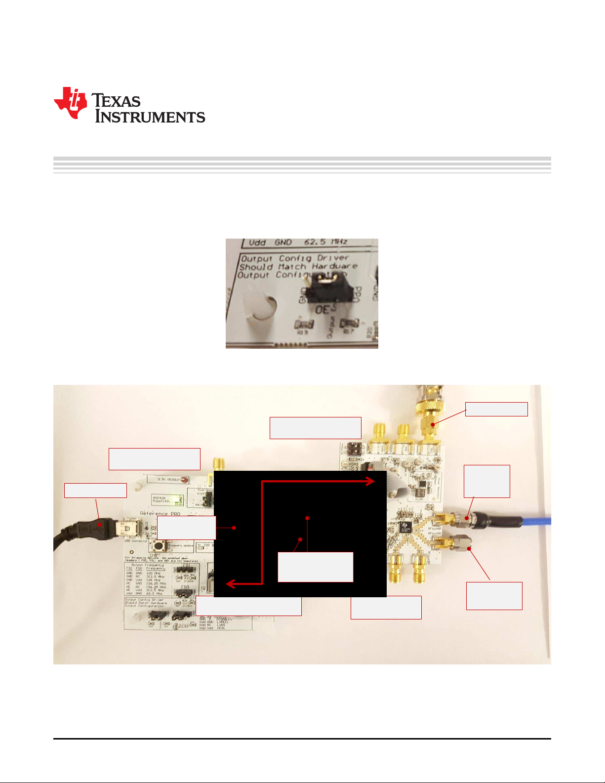
Appendix E
SNAU219–June 2017
Connecting Reference Pro
1. To use Reference Pro, change the configuration for SE or differential connection as shown on
Appendix D.
2. Change jumper position on Reference Pro, connect middle pin of OE header to Vdd.
Figure 16. Reference Pro Output Enable Header
The LMK61PD0A2 has several control pins dedicated for control of output format, output frequency, and
output enable control. These control pins can be configured through the jumpers shown in Table 5 and
Table 6.
18
Connecting Reference Pro
Figure 17. LMX2595EVM Setup With Reference Pro
Copyright © 2017, Texas Instruments Incorporated
Submit Documentation Feedback
SNAU219–June 2017
Page 19
www.ti.com
Jumpers FS1, FS0, OS, and OE can be used to configure the corresponding control pin to either high or
low state by strapping the center pin to VDD position (tie pins 2-3) or GND position (tie pins 1-2),
respectively. Connections from the VDD position to the device supply or from the GND position to the
ground plane are connected by 1.5-kΩ resistors.
Appendix E
Table 5. Output Frequency of LMK61PD0A2 (Reference Pro)
FS1 FS0 OUTPUT FREQUENCY (MHz)
0 0 100
0 NC 312.5
0 1 125
NC 0 106.25
NC NC 156.25
NC 1 212.5
1 0 62.5
Table 6. OutputType of LMK61PD0A2 (Reference Pro)
OS OE OUTPUT TYPE
X O Disabled (PLL Functional)
0 1 LVPECL
NC 1 LVDS
1 1 HCSL
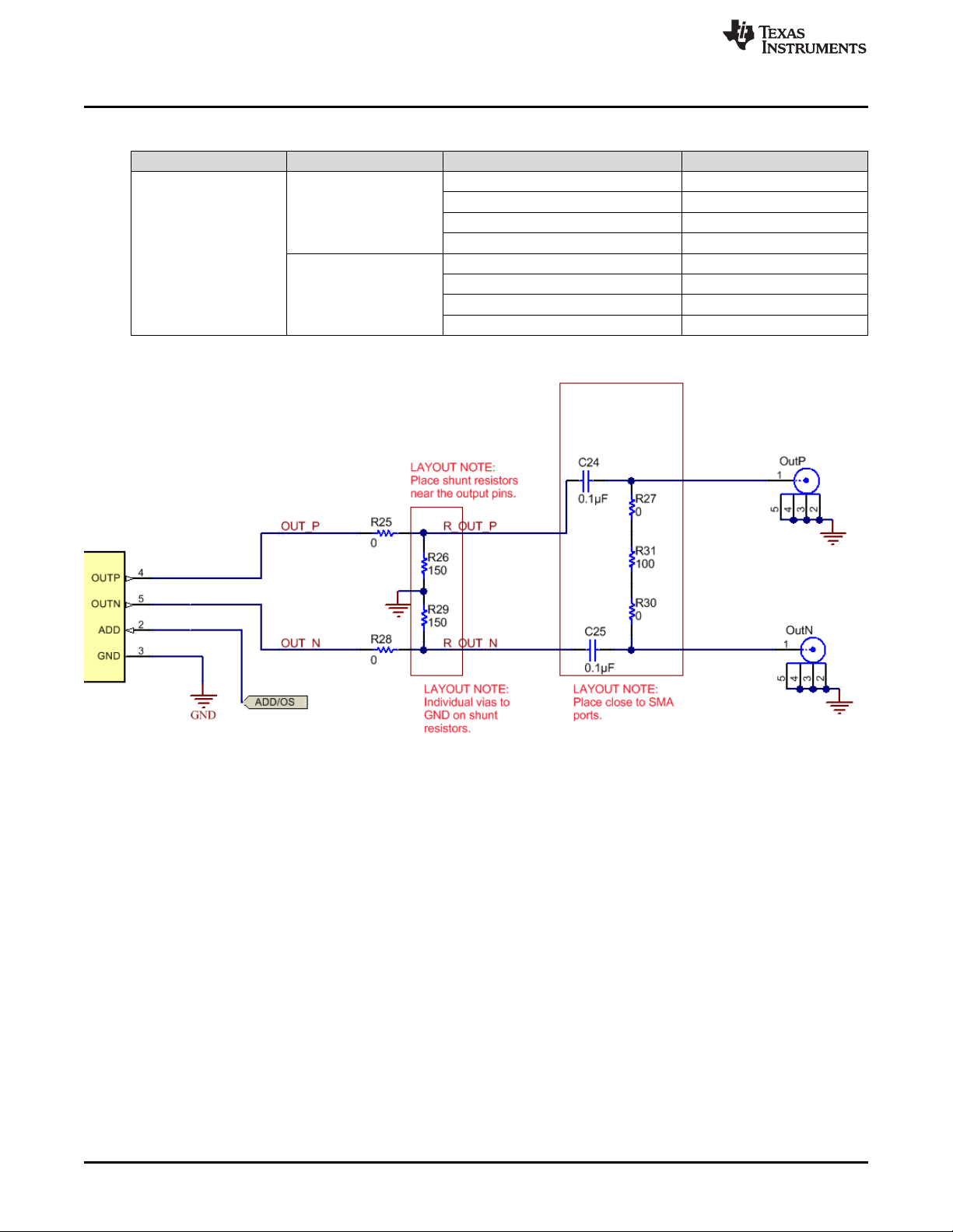
The OS pin is used to bias internal drivers and change the output type. It is imperative to match the output
termination passive components as shown on Table 7 with the output type from Table 6.
Table 7 lists component values for each configuration.
Table 7. Output Termination Schemes
OUTPUT FORMAT COUPLING COMPONENT VALUE
LVPECL AC
(2)
LVDS
(default EVM
configuration)
DC
AC R25, R28, R27, R30 0 Ω
DC R25, R27, R28, R30, C24, C25 0 Ω
(1)
R25, R28 0 Ω
R26, R29 150 Ω
C24, C25 0.01 uF
R27, R30, R31 DNP
R25, R28, C24, C25 0 Ω
R26, R29, R27, R30, R31 DNP
R31 100 Ω
C24, C25 0.01 uF
R26, R29 DNP
R31 100 Ω
R26, R29 DNP
(1)
50 Ω to VCC– 2? V termination is required on receiver.
(2)
100-Ω differential termination (R31) is provided on Reference Pro PCB. Removing the differential termination on the EVM is
possible if the differential termination is available on the receiver.
SNAU219–June 2017
Submit Documentation Feedback
Copyright © 2017, Texas Instruments Incorporated
Connecting Reference Pro
19
Page 20
Appendix E
OUTPUT FORMAT COUPLING COMPONENT VALUE
HCSL AC R25, R28 0 Ω
www.ti.com
Table 7. Output Termination Schemes (continued)
R26, R29 50 Ω
C24, C25 0 Ω
R27, R30, R31 DNP
DC R25, R28 0 Ω
R26, R29 50 Ω
C24, C25 0.01 uF
R27. R30, R31 DNP
20
Connecting Reference Pro
Figure 18. LMK61PD0A2 Output Termination
Copyright © 2017, Texas Instruments Incorporated
Submit Documentation Feedback
SNAU219–June 2017
Page 21
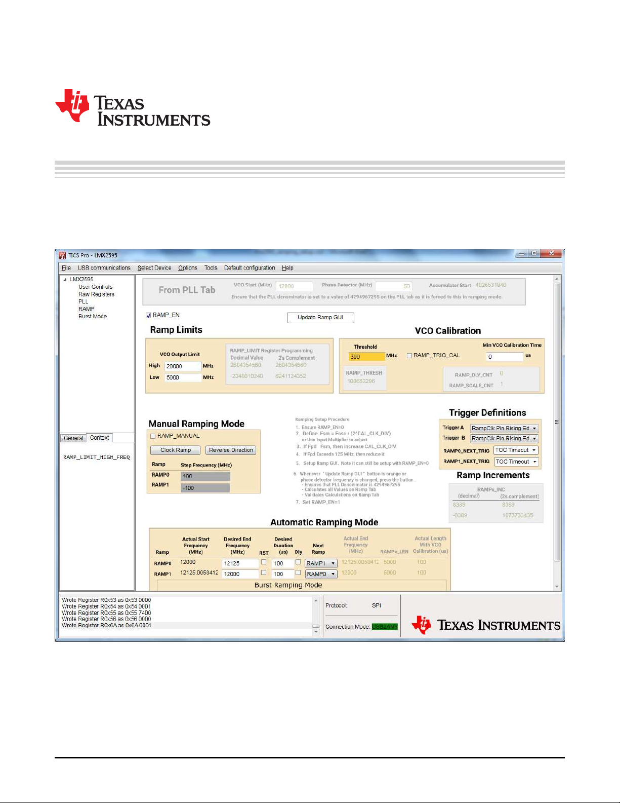
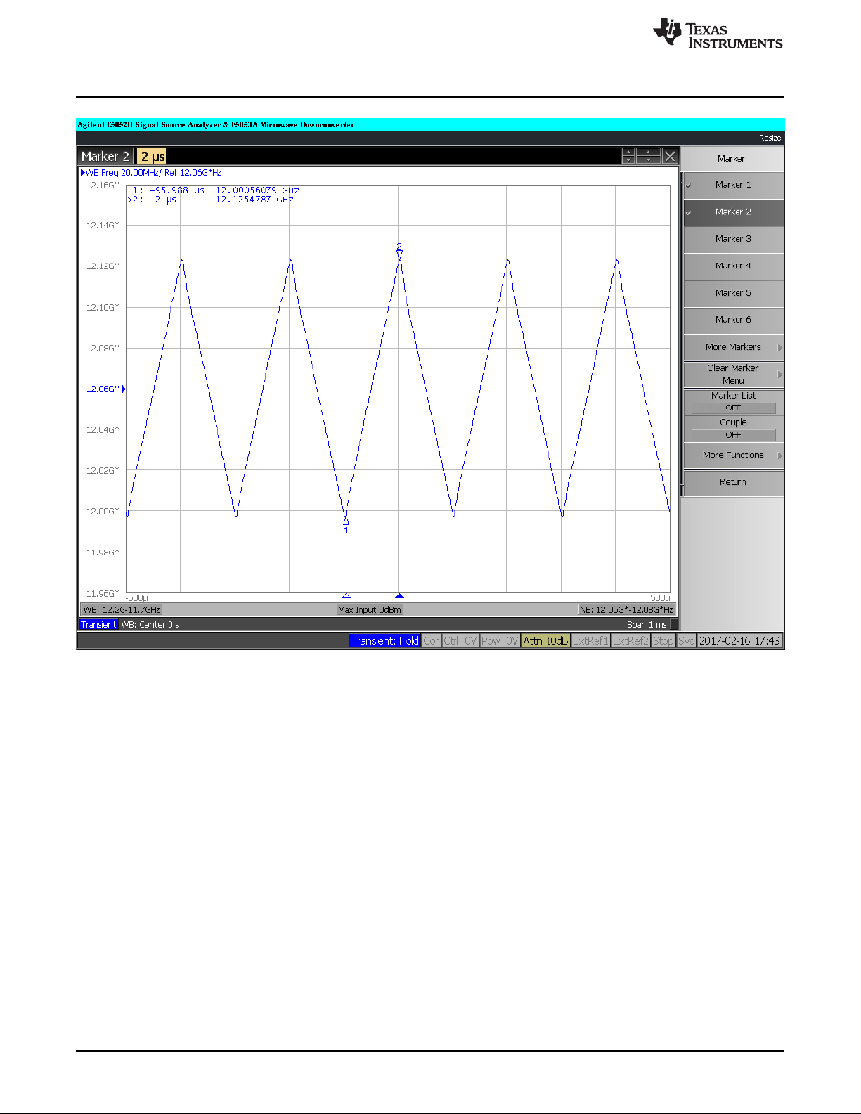
F.1 Ramping Example Waveform
VCO is ramping from 8 to 10 GHz and being dividing by 4 so that it can be seen with the HP53310A. This
can be set up on the ramp GUI tab.
Appendix F
SNAU219–June 2017
Ramping Feature
SNAU219–June 2017
Submit Documentation Feedback
Figure 19. Ramping Example Tics
Copyright © 2017, Texas Instruments Incorporated
Ramping Feature
21
Page 22
Ramping Example Waveform
www.ti.com
22
Ramping Feature
Figure 20. Ramping Example
Copyright © 2017, Texas Instruments Incorporated
Submit Documentation Feedback
SNAU219–June 2017
Page 23

1. Bring LMX2594 to a Lock State
2. Perform Sync
Appendix G
SNAU219–June 2017
SYSREF Feature
3. Configure TICS Pro PLL tab for SysRef
• Check the SYSREF_EN box
• Change OUTB_MUX to SysRef
• Uncheck the OUT_PD box
SNAU219–June 2017
Submit Documentation Feedback
Figure 21. Perform Sync For SysRef
Copyright © 2017, Texas Instruments Incorporated
SYSREF Feature
23
Page 24

Appendix G
www.ti.com
24
Figure 22. Configure and Enable SysRef
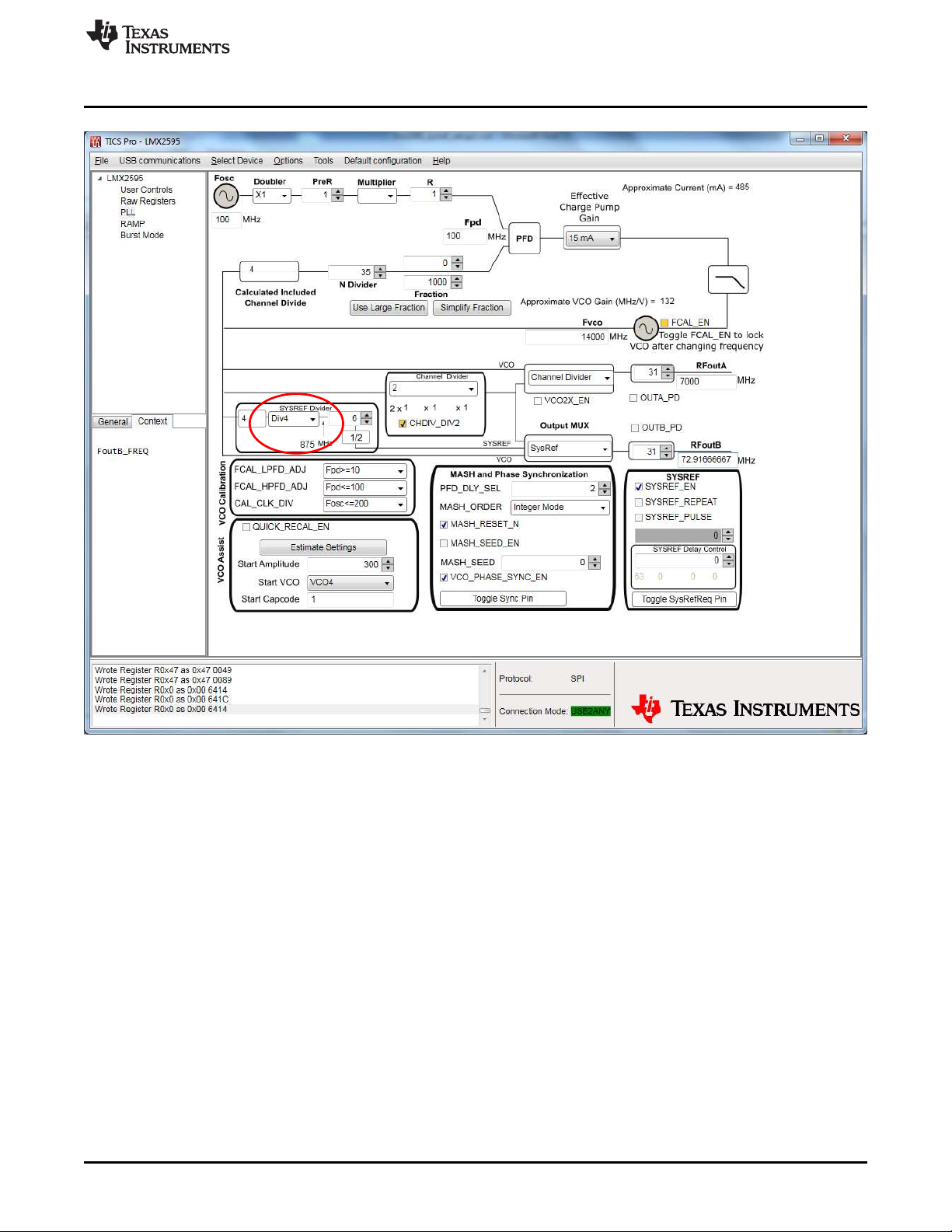
4. Confirm the Interpolator Frequency is between 800 MHz and 1500 MHz
• If not, change the SYSREF_DIV_PRE drop-down to Div2 or Div4 to reach an appropriate
Interpolator Frequency for the current configuration
SYSREF Feature
Copyright © 2017, Texas Instruments Incorporated
Submit Documentation Feedback
SNAU219–June 2017
Page 25
www.ti.com
Appendix G
5. Go to User Controls in the side bar and check the SysRefReq box under the Pins section
SNAU219–June 2017
Submit Documentation Feedback
Figure 23. Interpolator Frequency For SysRef
Copyright © 2017, Texas Instruments Incorporated
SYSREF Feature
25
Page 26

Appendix G
www.ti.com
26
Figure 24. Check SysRefReq Box on User Controls Tab
6. To modify SysRef Frequency, change the value in the SYSREF_DIV box
SYSREF Feature
Copyright © 2017, Texas Instruments Incorporated
Submit Documentation Feedback
SNAU219–June 2017
Page 27

www.ti.com
Appendix G
MODE NAME DESCRIPTION TICS PRO - SYS REF SETTINGS
Master -
Continuos
Master - Pulse
Repeater
SNAU219–June 2017
Submit Documentation Feedback
LMX2595 generates SysRef pulses as long as SysRefReq pin is held
SysRefReq pin is held high. Note: SysRefReq must be held high for
Figure 25. Modifying SysRef Frequency
Table 8. SysRef Modes
high.
LMX2595 generates a finite number of pulses as long as the
the duration of the pulses.
RFOUTB will repeat external input to SysRefReq pin. Output will be
reclocked to LMX2595 internal Frequency
Copyright © 2017, Texas Instruments Incorporated
Default mode. See quick start
instructions
• Uncheck SysRefReq under Pins
in User Controls tab
• Check SYSREF_PULSE
• Set SYSREF_PULSE_CNT to
desired number of pulses
• Check SysRefReq under Pins in
User Controls tab
• Uncheck SysRefReq
• Check SysRef_Repeat
SYSREF Feature
27
Page 28

Appendix H
SNAU219–June 2017
VCO Calibration
1. Connect an oscilloscope probe (high impedance) to MUXout of the device
2. Set trigger to about the center of the MUXout swing (approximately 1.6 V)
3. Set MUXOUT_SEL register R0[2] to a value of 1 for lock detect
4. Set your desired output frequency to lock to
5. Trigger the calibration with FCAL_EN register R0[3] to a value of 1
6. Observe the triggered pulse, there must be a pulse from MUXout digital HIGH to LOW and back to
HIGH (the low indicates the instant calibration is triggered and running, then high is when done
calibration). Adjust the time scale to capture the pulse (approximately 300 µs to start)
28
VCO Calibration
Figure 26. Unassisted Calibration TICS
Copyright © 2017, Texas Instruments Incorporated
Submit Documentation Feedback
SNAU219–June 2017
Page 29

www.ti.com
Appendix H
Figure 27. Unassisted Calibration Plot
SNAU219–June 2017
Submit Documentation Feedback
Copyright © 2017, Texas Instruments Incorporated
VCO Calibration
29
Page 30

Appendix I
SNAU219–June 2017
Enabling Onboard DC-DC Buck Converter (TPS62150)
30
Figure 28. Resistor Configuration to Enable DC-DC
1. MUST SWITCH R35 to Rtps1
2. MUST SWITCH R34 to Rtps2
3. Populate Rtps
4. DC-DC circuitry was optimized for efficiency for 5 to 8 V, but a voltage of 3.3 V to 17 V can be applied
to VCC SMA after resistor network is configured correctly from steps above.
Enabling Onboard DC-DC Buck Converter (TPS62150)
Copyright © 2017, Texas Instruments Incorporated
Submit Documentation Feedback
SNAU219–June 2017
Page 31

Appendix J
SNAU219–June 2017
Appendix J: Using the VCO Doubler
SNAU219–June 2017
Submit Documentation Feedback
Figure 29. VCO Frequency Doubler Setup in TICSPro
Appendix J: Using the VCO Doubler
Copyright © 2017, Texas Instruments Incorporated
31
Page 32
Appendix J
www.ti.com
Figure 30. 18 GHz Phase Noise using VCO Doubler
32
Appendix J: Using the VCO Doubler
Copyright © 2017, Texas Instruments Incorporated
Submit Documentation Feedback
SNAU219–June 2017
Page 33

STANDARD TERMS FOR EVALUATION MODULES
1. Delivery: TI delivers TI evaluation boards, kits, or modules, including any accompanying demonstration software, components, and/or
documentation which may be provided together or separately (collectively, an “EVM” or “EVMs”) to the User (“User”) in accordance
with the terms set forth herein. User's acceptance of the EVM is expressly subject to the following terms.
1.1 EVMs are intended solely for product or software developers for use in a research and development setting to facilitate feasibility
evaluation, experimentation, or scientific analysis of TI semiconductors products. EVMs have no direct function and are not
finished products. EVMs shall not be directly or indirectly assembled as a part or subassembly in any finished product. For
clarification, any software or software tools provided with the EVM (“Software”) shall not be subject to the terms and conditions
set forth herein but rather shall be subject to the applicable terms that accompany such Software
1.2 EVMs are not intended for consumer or household use. EVMs may not be sold, sublicensed, leased, rented, loaned, assigned,
or otherwise distributed for commercial purposes by Users, in whole or in part, or used in any finished product or production
system.
2 Limited Warranty and Related Remedies/Disclaimers:
2.1 These terms do not apply to Software. The warranty, if any, for Software is covered in the applicable Software License
Agreement.
2.2 TI warrants that the TI EVM will conform to TI's published specifications for ninety (90) days after the date TI delivers such EVM
to User. Notwithstanding the foregoing, TI shall not be liable for a nonconforming EVM if (a) the nonconformity was caused by
neglect, misuse or mistreatment by an entity other than TI, including improper installation or testing, or for any EVMs that have
been altered or modified in any way by an entity other than TI, (b) the nonconformity resulted from User's design, specifications
or instructions for such EVMs or improper system design, or (c) User has not paid on time. Testing and other quality control
techniques are used to the extent TI deems necessary. TI does not test all parameters of each EVM.
User's claims against TI under this Section 2 are void if User fails to notify TI of any apparent defects in the EVMs within ten (10)
business days after delivery, or of any hidden defects with ten (10) business days after the defect has been detected.
2.3 TI's sole liability shall be at its option to repair or replace EVMs that fail to conform to the warranty set forth above, or credit
User's account for such EVM. TI's liability under this warranty shall be limited to EVMs that are returned during the warranty
period to the address designated by TI and that are determined by TI not to conform to such warranty. If TI elects to repair or
replace such EVM, TI shall have a reasonable time to repair such EVM or provide replacements. Repaired EVMs shall be
warranted for the remainder of the original warranty period. Replaced EVMs shall be warranted for a new full ninety (90) day
warranty period.
3 Regulatory Notices:
3.1 United States
3.1.1 Notice applicable to EVMs not FCC-Approved:
FCC NOTICE: This kit is designed to allow product developers to evaluate electronic components, circuitry, or software
associated with the kit to determine whether to incorporate such items in a finished product and software developers to write
software applications for use with the end product. This kit is not a finished product and when assembled may not be resold or
otherwise marketed unless all required FCC equipment authorizations are first obtained. Operation is subject to the condition
that this product not cause harmful interference to licensed radio stations and that this product accept harmful interference.
Unless the assembled kit is designed to operate under part 15, part 18 or part 95 of this chapter, the operator of the kit must
operate under the authority of an FCC license holder or must secure an experimental authorization under part 5 of this chapter.
3.1.2 For EVMs annotated as FCC – FEDERAL COMMUNICATIONS COMMISSION Part 15 Compliant:
CAUTION
This device complies with part 15 of the FCC Rules. Operation is subject to the following two conditions: (1) This device may not
cause harmful interference, and (2) this device must accept any interference received, including interference that may cause
undesired operation.
Changes or modifications not expressly approved by the party responsible for compliance could void the user's authority to
operate the equipment.
FCC Interference Statement for Class A EVM devices
NOTE: This equipment has been tested and found to comply with the limits for a Class A digital device, pursuant to part 15 of
the FCC Rules. These limits are designed to provide reasonable protection against harmful interference when the equipment is
operated in a commercial environment. This equipment generates, uses, and can radiate radio frequency energy and, if not
installed and used in accordance with the instruction manual, may cause harmful interference to radio communications.
Operation of this equipment in a residential area is likely to cause harmful interference in which case the user will be required to
correct the interference at his own expense.
Page 34

FCC Interference Statement for Class B EVM devices
NOTE: This equipment has been tested and found to comply with the limits for a Class B digital device, pursuant to part 15 of
the FCC Rules. These limits are designed to provide reasonable protection against harmful interference in a residential
installation. This equipment generates, uses and can radiate radio frequency energy and, if not installed and used in accordance
with the instructions, may cause harmful interference to radio communications. However, there is no guarantee that interference
will not occur in a particular installation. If this equipment does cause harmful interference to radio or television reception, which
can be determined by turning the equipment off and on, the user is encouraged to try to correct the interference by one or more
of the following measures:
• Reorient or relocate the receiving antenna.
• Increase the separation between the equipment and receiver.
• Connect the equipment into an outlet on a circuit different from that to which the receiver is connected.
• Consult the dealer or an experienced radio/TV technician for help.
3.2 Canada
3.2.1 For EVMs issued with an Industry Canada Certificate of Conformance to RSS-210 or RSS-247
Concerning EVMs Including Radio Transmitters:
This device complies with Industry Canada license-exempt RSSs. Operation is subject to the following two conditions:
(1) this device may not cause interference, and (2) this device must accept any interference, including interference that may
cause undesired operation of the device.
Concernant les EVMs avec appareils radio:
Le présent appareil est conforme aux CNR d'Industrie Canada applicables aux appareils radio exempts de licence. L'exploitation
est autorisée aux deux conditions suivantes: (1) l'appareil ne doit pas produire de brouillage, et (2) l'utilisateur de l'appareil doit
accepter tout brouillage radioélectrique subi, même si le brouillage est susceptible d'en compromettre le fonctionnement.
Concerning EVMs Including Detachable Antennas:
Under Industry Canada regulations, this radio transmitter may only operate using an antenna of a type and maximum (or lesser)
gain approved for the transmitter by Industry Canada. To reduce potential radio interference to other users, the antenna type
and its gain should be so chosen that the equivalent isotropically radiated power (e.i.r.p.) is not more than that necessary for
successful communication. This radio transmitter has been approved by Industry Canada to operate with the antenna types
listed in the user guide with the maximum permissible gain and required antenna impedance for each antenna type indicated.
Antenna types not included in this list, having a gain greater than the maximum gain indicated for that type, are strictly prohibited
for use with this device.
Concernant les EVMs avec antennes détachables
Conformément à la réglementation d'Industrie Canada, le présent émetteur radio peut fonctionner avec une antenne d'un type et
d'un gain maximal (ou inférieur) approuvé pour l'émetteur par Industrie Canada. Dans le but de réduire les risques de brouillage
radioélectrique à l'intention des autres utilisateurs, il faut choisir le type d'antenne et son gain de sorte que la puissance isotrope
rayonnée équivalente (p.i.r.e.) ne dépasse pas l'intensité nécessaire à l'établissement d'une communication satisfaisante. Le
présent émetteur radio a été approuvé par Industrie Canada pour fonctionner avec les types d'antenne énumérés dans le
manuel d’usage et ayant un gain admissible maximal et l'impédance requise pour chaque type d'antenne. Les types d'antenne
non inclus dans cette liste, ou dont le gain est supérieur au gain maximal indiqué, sont strictement interdits pour l'exploitation de
l'émetteur
3.3 Japan
3.3.1 Notice for EVMs delivered in Japan: Please see http://www.tij.co.jp/lsds/ti_ja/general/eStore/notice_01.page 日本国内に
輸入される評価用キット、ボードについては、次のところをご覧ください。
http://www.tij.co.jp/lsds/ti_ja/general/eStore/notice_01.page
3.3.2 Notice for Users of EVMs Considered “Radio Frequency Products” in Japan: EVMs entering Japan may not be certified
by TI as conforming to Technical Regulations of Radio Law of Japan.
If User uses EVMs in Japan, not certified to Technical Regulations of Radio Law of Japan, User is required to follow the
instructions set forth by Radio Law of Japan, which includes, but is not limited to, the instructions below with respect to EVMs
(which for the avoidance of doubt are stated strictly for convenience and should be verified by User):
1. Use EVMs in a shielded room or any other test facility as defined in the notification #173 issued by Ministry of Internal
Affairs and Communications on March 28, 2006, based on Sub-section 1.1 of Article 6 of the Ministry’s Rule for
Enforcement of Radio Law of Japan,
2. Use EVMs only after User obtains the license of Test Radio Station as provided in Radio Law of Japan with respect to
EVMs, or
3. Use of EVMs only after User obtains the Technical Regulations Conformity Certification as provided in Radio Law of Japan
with respect to EVMs. Also, do not transfer EVMs, unless User gives the same notice above to the transferee. Please note
that if User does not follow the instructions above, User will be subject to penalties of Radio Law of Japan.
Page 35

【無線電波を送信する製品の開発キットをお使いになる際の注意事項】 開発キットの中には技術基準適合証明を受けて
いないものがあります。 技術適合証明を受けていないもののご使用に際しては、電波法遵守のため、以下のいずれかの
措置を取っていただく必要がありますのでご注意ください。
1. 電波法施行規則第6条第1項第1号に基づく平成18年3月28日総務省告示第173号で定められた電波暗室等の試験設備でご使用
いただく。
2. 実験局の免許を取得後ご使用いただく。
3. 技術基準適合証明を取得後ご使用いただく。
なお、本製品は、上記の「ご使用にあたっての注意」を譲渡先、移転先に通知しない限り、譲渡、移転できないものとします。
上記を遵守頂けない場合は、電波法の罰則が適用される可能性があることをご留意ください。 日本テキサス・イ
ンスツルメンツ株式会社
東京都新宿区西新宿6丁目24番1号
西新宿三井ビル
3.3.3 Notice for EVMs for Power Line Communication: Please see http://www.tij.co.jp/lsds/ti_ja/general/eStore/notice_02.page
電力線搬送波通信についての開発キットをお使いになる際の注意事項については、次のところをご覧ください。http:/
/www.tij.co.jp/lsds/ti_ja/general/eStore/notice_02.page
3.4 European Union
3.4.1 For EVMs subject to EU Directive 2014/30/EU (Electromagnetic Compatibility Directive):
This is a class A product intended for use in environments other than domestic environments that are connected to a
low-voltage power-supply network that supplies buildings used for domestic purposes. In a domestic environment this
product may cause radio interference in which case the user may be required to take adequate measures.
4 EVM Use Restrictions and Warnings:
4.1 EVMS ARE NOT FOR USE IN FUNCTIONAL SAFETY AND/OR SAFETY CRITICAL EVALUATIONS, INCLUDING BUT NOT
LIMITED TO EVALUATIONS OF LIFE SUPPORT APPLICATIONS.
4.2 User must read and apply the user guide and other available documentation provided by TI regarding the EVM prior to handling
or using the EVM, including without limitation any warning or restriction notices. The notices contain important safety information
related to, for example, temperatures and voltages.
4.3 Safety-Related Warnings and Restrictions:
4.3.1 User shall operate the EVM within TI’s recommended specifications and environmental considerations stated in the user
guide, other available documentation provided by TI, and any other applicable requirements and employ reasonable and
customary safeguards. Exceeding the specified performance ratings and specifications (including but not limited to input
and output voltage, current, power, and environmental ranges) for the EVM may cause personal injury or death, or
property damage. If there are questions concerning performance ratings and specifications, User should contact a TI
field representative prior to connecting interface electronics including input power and intended loads. Any loads applied
outside of the specified output range may also result in unintended and/or inaccurate operation and/or possible
permanent damage to the EVM and/or interface electronics. Please consult the EVM user guide prior to connecting any
load to the EVM output. If there is uncertainty as to the load specification, please contact a TI field representative.
During normal operation, even with the inputs and outputs kept within the specified allowable ranges, some circuit
components may have elevated case temperatures. These components include but are not limited to linear regulators,
switching transistors, pass transistors, current sense resistors, and heat sinks, which can be identified using the
information in the associated documentation. When working with the EVM, please be aware that the EVM may become
very warm.
4.3.2 EVMs are intended solely for use by technically qualified, professional electronics experts who are familiar with the
dangers and application risks associated with handling electrical mechanical components, systems, and subsystems.
User assumes all responsibility and liability for proper and safe handling and use of the EVM by User or its employees,
affiliates, contractors or designees. User assumes all responsibility and liability to ensure that any interfaces (electronic
and/or mechanical) between the EVM and any human body are designed with suitable isolation and means to safely
limit accessible leakage currents to minimize the risk of electrical shock hazard. User assumes all responsibility and
liability for any improper or unsafe handling or use of the EVM by User or its employees, affiliates, contractors or
designees.
4.4 User assumes all responsibility and liability to determine whether the EVM is subject to any applicable international, federal,
state, or local laws and regulations related to User’s handling and use of the EVM and, if applicable, User assumes all
responsibility and liability for compliance in all respects with such laws and regulations. User assumes all responsibility and
liability for proper disposal and recycling of the EVM consistent with all applicable international, federal, state, and local
requirements.
5. Accuracy of Information: To the extent TI provides information on the availability and function of EVMs, TI attempts to be as accurate
as possible. However, TI does not warrant the accuracy of EVM descriptions, EVM availability or other information on its websites as
accurate, complete, reliable, current, or error-free.
Page 36

6. Disclaimers:
6.1 EXCEPT AS SET FORTH ABOVE, EVMS AND ANY MATERIALS PROVIDED WITH THE EVM (INCLUDING, BUT NOT
LIMITED TO, REFERENCE DESIGNS AND THE DESIGN OF THE EVM ITSELF) ARE PROVIDED "AS IS" AND "WITH ALL
FAULTS." TI DISCLAIMS ALL OTHER WARRANTIES, EXPRESS OR IMPLIED, REGARDING SUCH ITEMS, INCLUDING BUT
NOT LIMITED TO ANY EPIDEMIC FAILURE WARRANTY OR IMPLIED WARRANTIES OF MERCHANTABILITY OR FITNESS
FOR A PARTICULAR PURPOSE OR NON-INFRINGEMENT OF ANY THIRD PARTY PATENTS, COPYRIGHTS, TRADE
SECRETS OR OTHER INTELLECTUAL PROPERTY RIGHTS.
6.2 EXCEPT FOR THE LIMITED RIGHT TO USE THE EVM SET FORTH HEREIN, NOTHING IN THESE TERMS SHALL BE
CONSTRUED AS GRANTING OR CONFERRING ANY RIGHTS BY LICENSE, PATENT, OR ANY OTHER INDUSTRIAL OR
INTELLECTUAL PROPERTY RIGHT OF TI, ITS SUPPLIERS/LICENSORS OR ANY OTHER THIRD PARTY, TO USE THE
EVM IN ANY FINISHED END-USER OR READY-TO-USE FINAL PRODUCT, OR FOR ANY INVENTION, DISCOVERY OR
IMPROVEMENT, REGARDLESS OF WHEN MADE, CONCEIVED OR ACQUIRED.
7. USER'S INDEMNITY OBLIGATIONS AND REPRESENTATIONS. USER WILL DEFEND, INDEMNIFY AND HOLD TI, ITS
LICENSORS AND THEIR REPRESENTATIVES HARMLESS FROM AND AGAINST ANY AND ALL CLAIMS, DAMAGES, LOSSES,
EXPENSES, COSTS AND LIABILITIES (COLLECTIVELY, "CLAIMS") ARISING OUT OF OR IN CONNECTION WITH ANY
HANDLING OR USE OF THE EVM THAT IS NOT IN ACCORDANCE WITH THESE TERMS. THIS OBLIGATION SHALL APPLY
WHETHER CLAIMS ARISE UNDER STATUTE, REGULATION, OR THE LAW OF TORT, CONTRACT OR ANY OTHER LEGAL
THEORY, AND EVEN IF THE EVM FAILS TO PERFORM AS DESCRIBED OR EXPECTED.
8. Limitations on Damages and Liability:
8.1 General Limitations. IN NO EVENT SHALL TI BE LIABLE FOR ANY SPECIAL, COLLATERAL, INDIRECT, PUNITIVE,
INCIDENTAL, CONSEQUENTIAL, OR EXEMPLARY DAMAGES IN CONNECTION WITH OR ARISING OUT OF THESE
TERMS OR THE USE OF THE EVMS , REGARDLESS OF WHETHER TI HAS BEEN ADVISED OF THE POSSIBILITY OF
SUCH DAMAGES. EXCLUDED DAMAGES INCLUDE, BUT ARE NOT LIMITED TO, COST OF REMOVAL OR
REINSTALLATION, ANCILLARY COSTS TO THE PROCUREMENT OF SUBSTITUTE GOODS OR SERVICES, RETESTING,
OUTSIDE COMPUTER TIME, LABOR COSTS, LOSS OF GOODWILL, LOSS OF PROFITS, LOSS OF SAVINGS, LOSS OF
USE, LOSS OF DATA, OR BUSINESS INTERRUPTION. NO CLAIM, SUIT OR ACTION SHALL BE BROUGHT AGAINST TI
MORE THAN TWELVE (12) MONTHS AFTER THE EVENT THAT GAVE RISE TO THE CAUSE OF ACTION HAS
OCCURRED.
8.2 Specific Limitations. IN NO EVENT SHALL TI'S AGGREGATE LIABILITY FROM ANY USE OF AN EVM PROVIDED
HEREUNDER, INCLUDING FROM ANY WARRANTY, INDEMITY OR OTHER OBLIGATION ARISING OUT OF OR IN
CONNECTION WITH THESE TERMS, , EXCEED THE TOTAL AMOUNT PAID TO TI BY USER FOR THE PARTICULAR
EVM(S) AT ISSUE DURING THE PRIOR TWELVE (12) MONTHS WITH RESPECT TO WHICH LOSSES OR DAMAGES ARE
CLAIMED. THE EXISTENCE OF MORE THAN ONE CLAIM SHALL NOT ENLARGE OR EXTEND THIS LIMIT.
9. Return Policy. Except as otherwise provided, TI does not offer any refunds, returns, or exchanges. Furthermore, no return of EVM(s)
will be accepted if the package has been opened and no return of the EVM(s) will be accepted if they are damaged or otherwise not in
a resalable condition. If User feels it has been incorrectly charged for the EVM(s) it ordered or that delivery violates the applicable
order, User should contact TI. All refunds will be made in full within thirty (30) working days from the return of the components(s),
excluding any postage or packaging costs.
10. Governing Law: These terms and conditions shall be governed by and interpreted in accordance with the laws of the State of Texas,
without reference to conflict-of-laws principles. User agrees that non-exclusive jurisdiction for any dispute arising out of or relating to
these terms and conditions lies within courts located in the State of Texas and consents to venue in Dallas County, Texas.
Notwithstanding the foregoing, any judgment may be enforced in any United States or foreign court, and TI may seek injunctive relief
in any United States or foreign court.
Mailing Address: Texas Instruments, Post Office Box 655303, Dallas, Texas 75265
Copyright © 2017, Texas Instruments Incorporated
Page 37

IMPORTANT NOTICE FOR TI DESIGN INFORMATION AND RESOURCES
Texas Instruments Incorporated (‘TI”) technical, application or other design advice, services or information, including, but not limited to,
reference designs and materials relating to evaluation modules, (collectively, “TI Resources”) are intended to assist designers who are
developing applications that incorporate TI products; by downloading, accessing or using any particular TI Resource in any way, you
(individually or, if you are acting on behalf of a company, your company) agree to use it solely for this purpose and subject to the terms of
this Notice.
TI’s provision of TI Resources does not expand or otherwise alter TI’s applicable published warranties or warranty disclaimers for TI
products, and no additional obligations or liabilities arise from TI providing such TI Resources. TI reserves the right to make corrections,
enhancements, improvements and other changes to its TI Resources.
You understand and agree that you remain responsible for using your independent analysis, evaluation and judgment in designing your
applications and that you have full and exclusive responsibility to assure the safety of your applications and compliance of your applications
(and of all TI products used in or for your applications) with all applicable regulations, laws and other applicable requirements. You
represent that, with respect to your applications, you have all the necessary expertise to create and implement safeguards that (1)
anticipate dangerous consequences of failures, (2) monitor failures and their consequences, and (3) lessen the likelihood of failures that
might cause harm and take appropriate actions. You agree that prior to using or distributing any applications that include TI products, you
will thoroughly test such applications and the functionality of such TI products as used in such applications. TI has not conducted any
testing other than that specifically described in the published documentation for a particular TI Resource.
You are authorized to use, copy and modify any individual TI Resource only in connection with the development of applications that include
the TI product(s) identified in such TI Resource. NO OTHER LICENSE, EXPRESS OR IMPLIED, BY ESTOPPEL OR OTHERWISE TO
ANY OTHER TI INTELLECTUAL PROPERTY RIGHT, AND NO LICENSE TO ANY TECHNOLOGY OR INTELLECTUAL PROPERTY
RIGHT OF TI OR ANY THIRD PARTY IS GRANTED HEREIN, including but not limited to any patent right, copyright, mask work right, or
other intellectual property right relating to any combination, machine, or process in which TI products or services are used. Information
regarding or referencing third-party products or services does not constitute a license to use such products or services, or a warranty or
endorsement thereof. Use of TI Resources may require a license from a third party under the patents or other intellectual property of the
third party, or a license from TI under the patents or other intellectual property of TI.
TI RESOURCES ARE PROVIDED “AS IS” AND WITH ALL FAULTS. TI DISCLAIMS ALL OTHER WARRANTIES OR
REPRESENTATIONS, EXPRESS OR IMPLIED, REGARDING TI RESOURCES OR USE THEREOF, INCLUDING BUT NOT LIMITED TO
ACCURACY OR COMPLETENESS, TITLE, ANY EPIDEMIC FAILURE WARRANTY AND ANY IMPLIED WARRANTIES OF
MERCHANTABILITY, FITNESS FOR A PARTICULAR PURPOSE, AND NON-INFRINGEMENT OF ANY THIRD PARTY INTELLECTUAL
PROPERTY RIGHTS.
TI SHALL NOT BE LIABLE FOR AND SHALL NOT DEFEND OR INDEMNIFY YOU AGAINST ANY CLAIM, INCLUDING BUT NOT
LIMITED TO ANY INFRINGEMENT CLAIM THAT RELATES TO OR IS BASED ON ANY COMBINATION OF PRODUCTS EVEN IF
DESCRIBED IN TI RESOURCES OR OTHERWISE. IN NO EVENT SHALL TI BE LIABLE FOR ANY ACTUAL, DIRECT, SPECIAL,
COLLATERAL, INDIRECT, PUNITIVE, INCIDENTAL, CONSEQUENTIAL OR EXEMPLARY DAMAGES IN CONNECTION WITH OR
ARISING OUT OF TI RESOURCES OR USE THEREOF, AND REGARDLESS OF WHETHER TI HAS BEEN ADVISED OF THE
POSSIBILITY OF SUCH DAMAGES.
You agree to fully indemnify TI and its representatives against any damages, costs, losses, and/or liabilities arising out of your noncompliance with the terms and provisions of this Notice.
This Notice applies to TI Resources. Additional terms apply to the use and purchase of certain types of materials, TI products and services.
These include; without limitation, TI’s standard terms for semiconductor products http://www.ti.com/sc/docs/stdterms.htm), evaluation
modules, and samples (http://www.ti.com/sc/docs/sampterms.htm).
Mailing Address: Texas Instruments, Post Office Box 655303, Dallas, Texas 75265
Copyright © 2017, Texas Instruments Incorporated
Page 38

Mouser Electronics
Authorized Distributor
Click to View Pricing, Inventory, Delivery & Lifecycle Information:
Texas Instruments:
LMX2595EVM
 Loading...