

User's Guide
SNAU217A–August 2017–Revised November 2017
LMX2572EVM Evaluation Instructions
The LMX2572EVM is design to evaluate the performance of LMX2572. This board consists of a LMX2572
device.
The LMX2572 is a low-power, high-performance wideband synthesizer that can generate any frequency
from 12.5 MHz to 6.4 GHz without using an internal VCO doubler. The PLL delivers excellent performance
while consuming just 75 mA from a single 3.3-V supply.
1 LMX2572EVM Evaluation Module......................................................................................... 3
2 Setup .......................................................................................................................... 3
3 Typical Measurement ....................................................................................................... 5
4 Schematic ................................................................................................................... 13
5 PCB Layout and Layer Stack-up......................................................................................... 15
6 Bill of Materials ............................................................................................................. 18
7 Troubleshooting Guide .................................................................................................... 19
Appendix A Using Different Reference Clock ................................................................................ 20
Appendix B Reference PRO.................................................................................................... 21
1 EVM Connection Diagram.................................................................................................. 3
2 Select Device in TICS Pro.................................................................................................. 4
3 Default Mode ................................................................................................................. 5
4 MUXout_SW Switch......................................................................................................... 5
5 Loop Filter .................................................................................................................... 6
6 Default Output................................................................................................................ 6
7 Phase Adjustment Setting .................................................................................................. 7
SNAU217A–August 2017–Revised November 2017
Submit Documentation Feedback
Contents
List of Figures
Copyright © 2017, Texas Instruments Incorporated
LMX2572EVM Evaluation Instructions
1

www.ti.com
8 Phase Adjustment ........................................................................................................... 7
9 Calibration-Free Automatic Ramp Setting................................................................................ 8
10 Calibration-Free Automatic Ramp ......................................................................................... 8
11 Automatic Ramp Setting.................................................................................................... 9
12 Automatic Ramp ............................................................................................................. 9
13 SYSREF Pulsed Mode Setting........................................................................................... 10
14 SYSREF Pulsed Mode .................................................................................................... 10
15 FSK SPI FAST Mode Setting............................................................................................. 11
16 FSK SPI FAST Mode...................................................................................................... 11
17 Readback Setting .......................................................................................................... 12
18 Register Readback......................................................................................................... 12
19 LMX2572EVM Schematic (Page 1)...................................................................................... 13
20 LMX2572EVM Schematic (Page 2)...................................................................................... 14
21 PCB Layer Stack-Up....................................................................................................... 15
22 Top Layer ................................................................................................................... 15
23 GND Layer .................................................................................................................. 16
24 Power Layer ................................................................................................................ 16
25 Bottom Layer................................................................................................................ 17
26 Troubleshooting Guide .................................................................................................... 19
27 Output Termination Schematic ........................................................................................... 22
28 Default Output Phase Nosie.............................................................................................. 23
29 Default Output Waveform ................................................................................................. 23
30 Firmware Requirement .................................................................................................... 23
31 Firmware Loader ........................................................................................................... 24
32 BSL Button .................................................................................................................. 24
33 Update Firmware........................................................................................................... 25
34 Firmware Update Completed ............................................................................................. 25
35 USB Communications ..................................................................................................... 26
1 Loop Filter Configuration.................................................................................................... 5
2 Phase Adjustment Setting .................................................................................................. 7
3 Calibration-free Automatic Ramp Example............................................................................... 8
4 Automatic Ramp Example.................................................................................................. 9
5 FSK SPI FAST Mode Example........................................................................................... 11
6 Bill of Materials ............................................................................................................. 18
7 Reference Clock Input Configuration.................................................................................... 20
8 Reference PRO Output Frequency Selection .......................................................................... 21
9 Reference PRO Output Format Selection .............................................................................. 22
10 Output Termination Configuration........................................................................................ 22
Trademarks
All trademarks are the property of their respective owners.
2
LMX2572EVM Evaluation Instructions
List of Tables
SNAU217A–August 2017–Revised November 2017
Copyright © 2017, Texas Instruments Incorporated
Submit Documentation Feedback

50
50
www.ti.com
1 LMX2572EVM Evaluation Module
1.1 Evaluation Module Contents
In the box, there are:
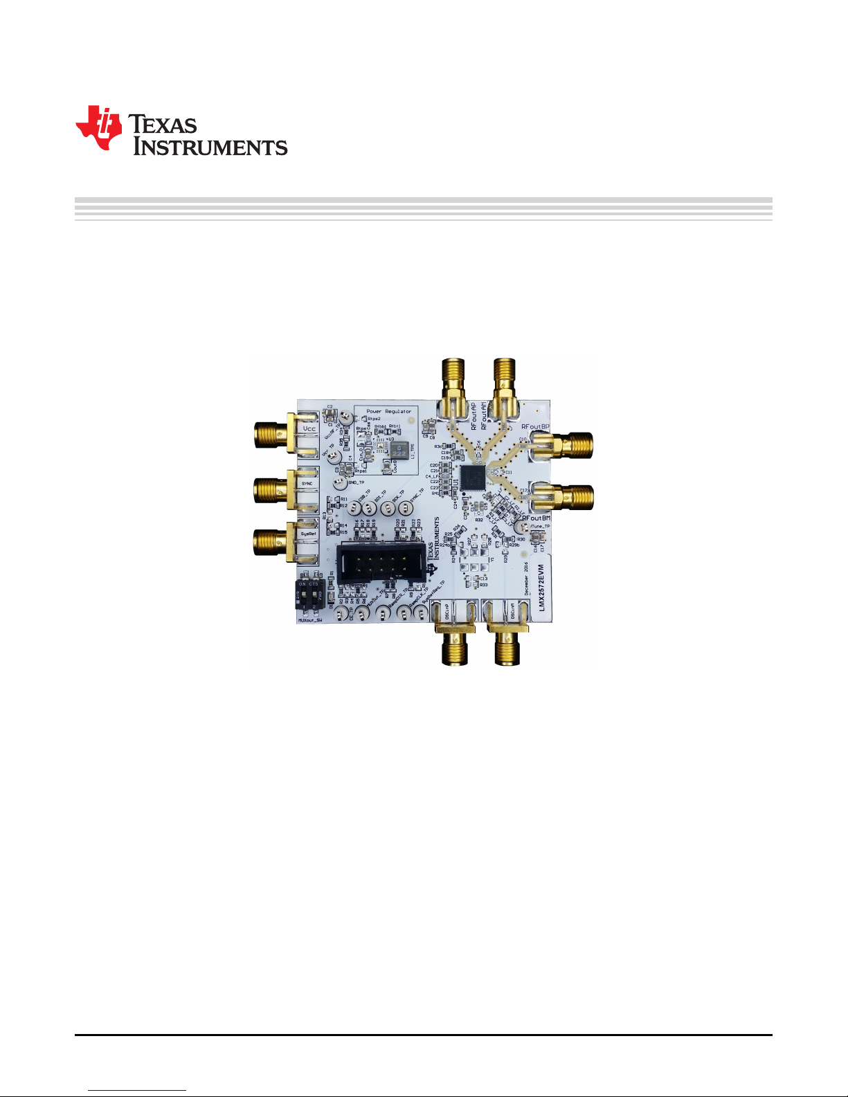
• One LMX2572EVM board (SV601308-003).
• One Reference PRO board (SV601349).
• Two SMA Male-to-Male adaptors (132168).
• One USB cable.
• One 10-pin ribbon cable.
1.2 Evaluation Setup Requirement
The evaluation will require the following hardware and software:
• A DC power supply
• A spectrum analyzer or a signal analyzer
• A PC running Windows 7 or more recent version
• An oscilloscope (optional)
• A high quality signal generator (optional)
• Texas Instruments Clocks and Synthesizers TICS Pro software
• Texas Instruments PLLatinum Simulator Tool (optional)
LMX2572EVM Evaluation Module
1.3 Resources
Related evaluation and development resources are as follows:
• LMX2572 data sheet
• TICS Pro software
• PLLatinum Simulator Tool (PLL Sim)
2 Setup
2.1 Connection Diagram
SNAU217A–August 2017–Revised November 2017
Submit Documentation Feedback
Figure 1. EVM Connection Diagram
Copyright © 2017, Texas Instruments Incorporated
LMX2572EVM Evaluation Instructions
3
Setup
2.2 Power Supply
Apply 3.3 V to VCCSMA connector. Acceptable supply voltage range is 3 V to 3.6 V. The maximum current
consumption in the most extreme configuration must not exceed 150 mA.
By default, the onboard DC-DC converter is not used.
2.3 Reference Clock
Connect OSCinP SMA connector with one of the outputs from Reference PRO using the SMA Male-tomale adopter. OSCinM SMA connector is not connected to LMX2572 so it could be left open.
The EVM is configured for single-ended input with OSCin pin connected to OSCinP SMA connector and
OSCinM pin 50-Ω terminated onboard. If required, the EVM can be modified to operate with different clock
source in different configuration, see Appendix A for details.
Terminate the unused output of the Reference PRO board with a 50-Ω resistor or SMA load. By default,
the output clock from Reference PRO is a 100-MHz LVPECL clock. Appendix B has the details of
Reference PRO.
2.4 RF Output
Connect either RFoutAP or RFoutAM SMA connector to a signal analyzer. The unused connector must be
terminated with a 50-Ω resistor or SMA load. Output frequency is 3 GHz and the amplitude is about +2.5
dBm.
By default, the evaluation software, TICS Pro, has RFoutB power down. These SMA connectors could be
left open.
www.ti.com
2.5 Programming
Connect ribbon cable from Reference PRO to LMX2572EVM.
Connect USB cable from a PC to USB port in Reference PRO. This provides power supply to Reference
PRO board and communication with TICS Pro. A firmware update may be required, see Appendix B for
details.
2.6 Evaluation Software
Download and install TICS Pro to a PC.
Run the software and follow the following steps to get started.
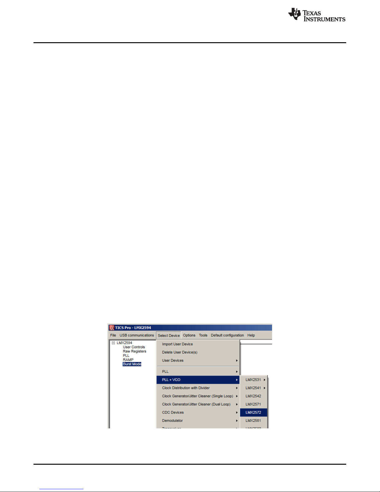
1. Go to "Select Device" → "PLL + VCO" → LMX2572.
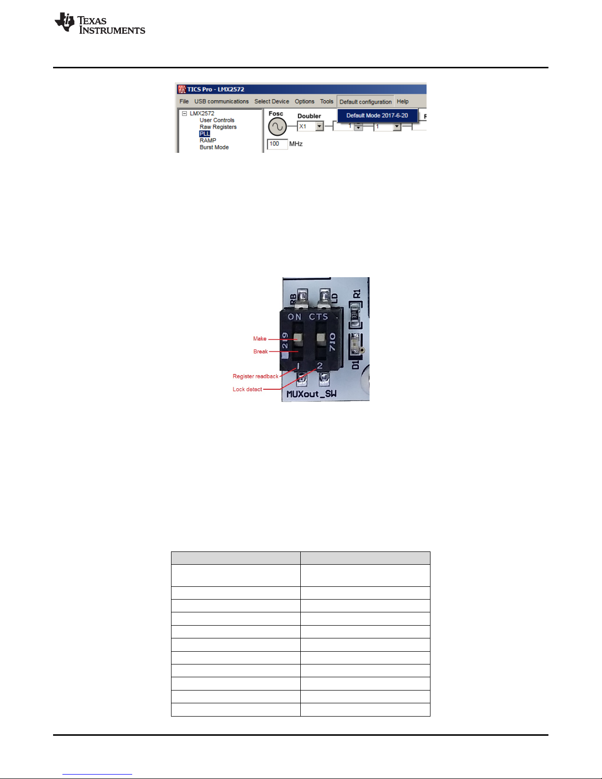
2. Go to "Default Configuration" → "Default Mode xxxx-xx-xx".
4
LMX2572EVM Evaluation Instructions
Figure 2. Select Device in TICS Pro
SNAU217A–August 2017–Revised November 2017
Copyright © 2017, Texas Instruments Incorporated
Submit Documentation Feedback
www.ti.com
2.7 EVM Strap Options
2.7.1 MUXout_SW
There are two switches in MUXout_SW. Switch 1 is used for register readback. Switch 2 is used to
provide a visual PLL lock status through the LED D1. By default, both switches are in the Make position.
To read back register in TICS Pro, set Switch 2 to the Break position.
Setup
Figure 3. Default Mode
3 Typical Measurement
3.1 Default Configuration
3.1.1 Loop Filter
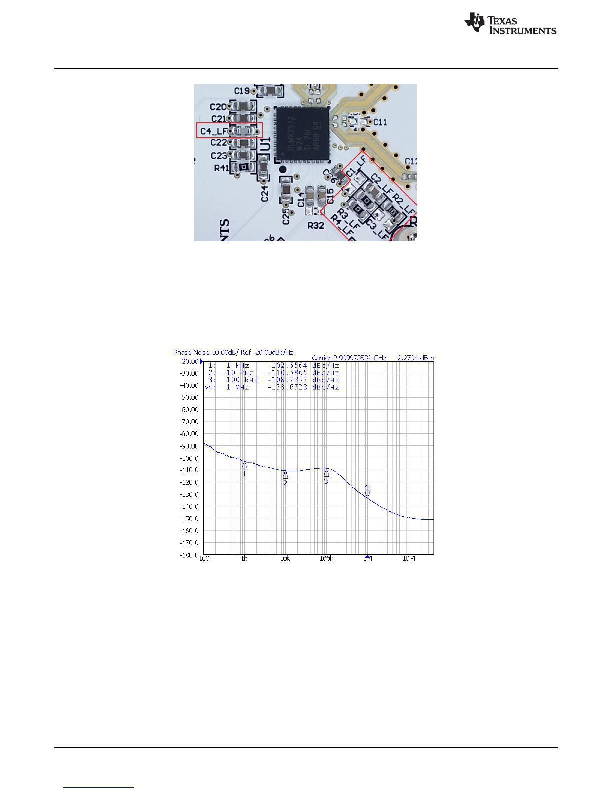
The parameters for the loop filter are:
Figure 4. MUXout_SW Switch
Table 1. Loop Filter Configuration
PARAMETER VALUE
VCO frequency
VCO gain 66 MHz/V
Effective charge pump gain 2500 µA
Phase detector frequency 100 MHz
Loop bandwidth 115 kHz
Phase margin 48 degrees
C1_LF, C3_LF Open
C2_LF 15 nF
C4_LF 2.2 nF
R2_LF 330 Ω
R3_LF, R4_LF 0 Ω
Designed for 6 GHz, but works
over the whole frequency range
SNAU217A–August 2017–Revised November 2017
Submit Documentation Feedback
Copyright © 2017, Texas Instruments Incorporated
LMX2572EVM Evaluation Instructions
5
Typical Measurement
3.1.2 Typical Output
1. Follow Section 2 to setup the evaluation.
2. Click "Write All Registers" to write all the registers to LMX2572.
Default output is 3 GHz.
www.ti.com
Figure 5. Loop Filter
3.2 Additional Tests
3.2.1 Phase Adjustment
The phase of the RF output signal can be adjusted as follows:
Phase shift in degree = 360° × (MASH_SEED / PLL_DEN) × (P / CHDIV), where P = 2 when
VCO_PHASE_SYNC_EN = 1, else P = 1.
Here is an example.
6
LMX2572EVM Evaluation Instructions
Figure 6. Default Output
SNAU217A–August 2017–Revised November 2017
Copyright © 2017, Texas Instruments Incorporated
Submit Documentation Feedback

www.ti.com
Phase shift = 360° × (800 / 1000) × (1 / 32) = 9°. We can write 800 to MASH_SEED 40 times to get 360°
phase shift.
Typical Measurement
Table 2. Phase Adjustment Setting
PARAMETER EXAMPLE VALUE
MASH_SEED 800
PLL_DEN 1000
CHDIV 32
VCO_PHASE_SYNC_EN 0
Figure 7. Phase Adjustment Setting
3.2.2 Calibration-free Automatic Ramping
LMX2572 supports linear frequency ramp without the need of VCO calibration in the middle of the ramp.
The output waveform is a continuous frequency sweep between the start and the end frequencies.
However, the frequency ramp range is limited. When using ramp, the followings need to be set
accordingly:
• OUT_FORCE = 1
• LD_DLY = 0
• PLL_DEN = 232– 1
SNAU217A–August 2017–Revised November 2017
Submit Documentation Feedback
Figure 8. Phase Adjustment
Copyright © 2017, Texas Instruments Incorporated
LMX2572EVM Evaluation Instructions
7

Typical Measurement
This is a triangular ramp example. Ramp up is defined by RAMP0 while ramp down is defined by RAMP1.
RAMP_THRESH, RAMP_DLY_CNT, and RAMP_SCALE_COUNT are "don't care" because we are not
going to trigger any VCO calibration. RAMP_MANUAL = 0 means Automatic Ramping mode.
Set RAMP_EN = 1 to start ramping. Set RAMP_EN = 0 to turn off ramping.
www.ti.com
Table 3. Calibration-free Automatic Ramp Example
PARAMETER EXAMPLE VALUE
Ramping start frequency 4795 MHz
Ramping stop frequency 4805 MHz
Phase detector frequency 50 MHz
Ramp up / down time 200 µs
RAMP_LIMIT_HIGH 4995 MHz
RAMP_LIMIT_LOW 4595 MHz
Figure 9. Calibration-Free Automatic Ramp Setting
Figure 10. Calibration-Free Automatic Ramp
8
LMX2572EVM Evaluation Instructions
SNAU217A–August 2017–Revised November 2017
Copyright © 2017, Texas Instruments Incorporated
Submit Documentation Feedback

www.ti.com
3.2.3 Automatic Ramping
This ramping mode supports wider ramp frequency, however there are glitches in the middle of the ramp
because of VCO calibrations which are required so as to ensure the continuity of the ramp.
Table 4. Automatic Ramp Example
PARAMETER EXAMPLE VALUE
Ramping start frequency 4740 MHz
Ramping stop frequency 4860 MHz
Phase detector frequency 50 MHz
Ramp up / down time 1000 µs
RAMP_LIMIT_HIGH 5060 MHz
RAMP_LIMIT_LOW 4540 MHz
f
OSCin
CAL_CLK_DIV 0
RAMP_THRESH 40 MHz
Pause time for VCO calibration 500 µs
100 MHz
Typical Measurement
SNAU217A–August 2017–Revised November 2017
Submit Documentation Feedback
Figure 11. Automatic Ramp Setting
Figure 12. Automatic Ramp
Copyright © 2017, Texas Instruments Incorporated
LMX2572EVM Evaluation Instructions
9

Typical Measurement
3.2.4 SYSREF Example
RFoutB of LMX2572 can be used to generate or duplicate SYSREF signal. The output of RFoutB can be a
single pulse, series of pulse, or a continuous stream of pulses. These pulses are synchronous with the
RFoutA signal with an adjustable delay. To use the SYSREF capability, the PLL must be in SYNC mode
with VCO_PHASE_SYNC_EN = 1. Here is an example of Pulsed mode.
www.ti.com
10
LMX2572EVM Evaluation Instructions
Figure 13. SYSREF Pulsed Mode Setting
Figure 14. SYSREF Pulsed Mode
SNAU217A–August 2017–Revised November 2017
Copyright © 2017, Texas Instruments Incorporated
Submit Documentation Feedback
 Loading...