

Texas Instruments LM3671LC, LM3671LC-1.2, LM3671LC-1.3, LM3671LC-1.6, LM3671LC-1.8 User Manual
...
1
2
5
43
V
IN
SW
FB
EN
GND
L1: 2.2 PH
V
OUT
C
OUT
10 PF
C
IN
4.7 PF
LM3671
V
IN
2.7V to 5.5V
www.ti.com
SNVS294P –NOVEMBER 2004–REVISED MAY 2013
LM3671, LM3671Q 2MHz, 600mA Step-Down DC-DC Converter
Check for Samples: LM3671, LM3671Q
1
FEATURES
2
• 16 µA Typical Quiescent Current
• 600 mA Maximum Load Capability • PDAs
• 2 MHz PWM Fixed Switching Frequency (typ.) • MP3 Players
• Automatic PFM/PWM Mode Switching • W-LAN
• Internal Synchronous Rectification for High • Portable Instruments
Efficiency
• Internal Soft start
• 0.01 µA Typical Shutdown Current
• Operates from a Single Li-Ion Cell Battery
• Only Three Tiny Surface-Mount External
Components Required (One Inductor, Two
Ceramic Capacitors)
• Current Overload and Thermal Shutdown
Protection
• Available in Fixed Output Voltages and
Adjustable Version
• LM3671Q is an Automotive Grade Product that
is AEC-Q100 Grade 1 Qualified
• SOT-23, 5-Bump DSBGA and 6-Pin USON
Packages
APPLICATIONS
• Mobile Phones
• Digital Still Cameras
• Portable Hard Disk Drives
• Automotive
DESCRIPTION
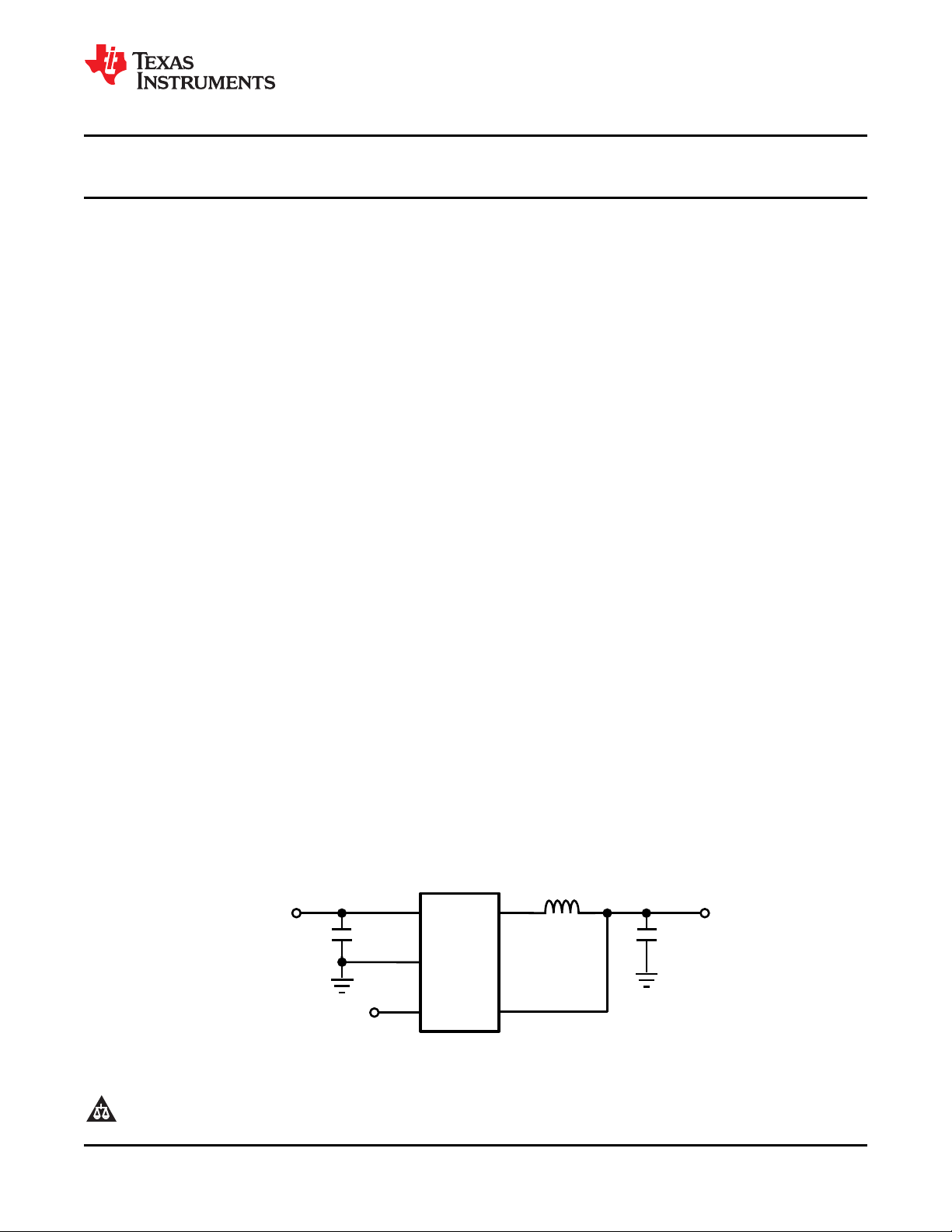
The LM3671 step-down DC-DC converter is
optimized for powering low voltage circuits from a
single Li-Ion cell battery and input voltage rails from
2.7V to 5.5V. It provides up to 600 mA load current,
over the entire input voltage range. There are several
different fixed voltage output options available as well
as an adjustable output voltage version range from
1.1V to 3.3V.
The device offers superior features and performance
for mobile phones and similar portable systems.
Automatic intelligent switching between PWM lownoise and PFM low-current mode offers improved
system control. During PWM mode, the device
operates at a fixed-frequency of 2 MHz (typ.).
Hysteretic PFM mode extends the battery life by
reducing the quiescent current to 16 µA (typ.) during
light load and standby operation. Internal
synchronous rectification provides high efficiency
during PWM mode operation. In shutdown mode, the
device turns off and reduces battery consumption to
0.01 µA (typ.).
LM3671
LM3671Q
TYPICAL APPLICATION CIRCUITS
Figure 1. Typical Application Circuit
1
2All trademarks are the property of their respective owners.
PRODUCTION DATA information is current as of publication date.
Products conform to specifications per the terms of the Texas
Instruments standard warranty. Production processing does not
necessarily include testing of all parameters.
Please be aware that an important notice concerning availability, standard warranty, and use in critical applications of
Texas Instruments semiconductor products and disclaimers thereto appears at the end of this data sheet.
Copyright © 2004–2013, Texas Instruments Incorporated
A3
Top View Bottom View
A1
C1
A3
C3
EN
FB
SW
GND
V
IN
EN
GND
SW
FB
B2
V
IN
A1
C3
C1
B2
V
IN
1
GND2EN
3
FB
4
SW
5
1
2
5
43
V
IN
SW
FB
EN
GND
L1: 2.2 PH
V
OUT
C
OUT
10 PF
C
IN
4.7 PF
LM3671-
ADJ
V
IN
2.7V to 5.5V
R1
R2
C1
C2
LM3671
LM3671Q
SNVS294P –NOVEMBER 2004–REVISED MAY 2013
DESCRIPTION (CONTINUED)
The LM3671 is available in SOT-23, tiny 5-bump DSBGA and a 6-pin USON packages in leaded (PB) and leadfree (NO PB) versions. A high-switching frequency of 2 MHz (typ.) allows use of tiny surface-mount components.
Only three external surface-mount components, an inductor and two ceramic capacitors, are required.
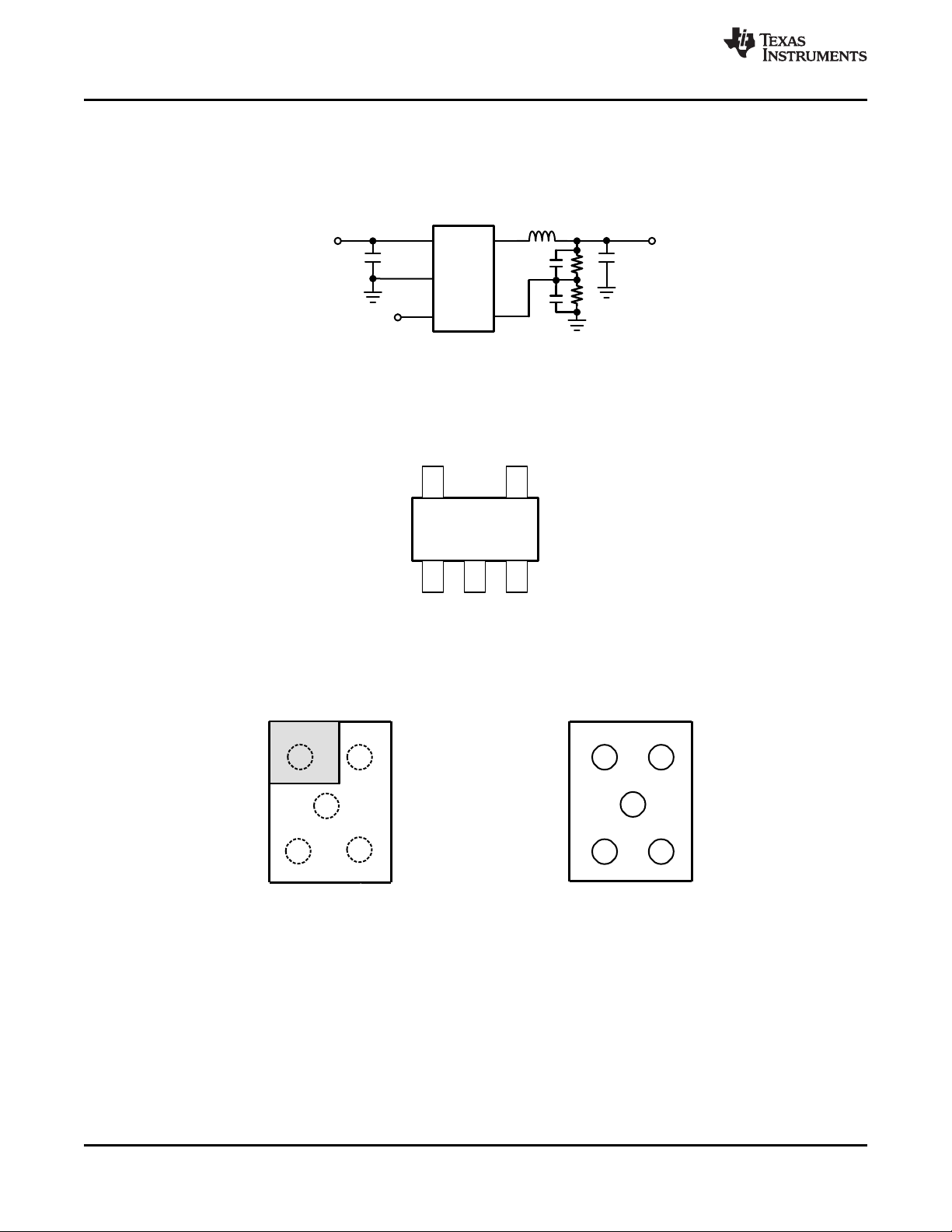
Figure 2. Typical Application Circuit for ADJ version
Connection Diagrams
www.ti.com
Figure 3. Top View
SOT-23 Package
See Package Number DBV (2.92 mm x 2.84 mm x 1.2 mm)
Figure 4. 5-Bump DSBGA Package
See Package Number YZR0005 (1.05 mm x 1.38 mm x 0.6 mm)
2 Submit Documentation Feedback Copyright © 2004–2013, Texas Instruments Incorporated
Product Folder Links: LM3671 LM3671Q

1
3 4
6
En
Pgnd
Vin
2
5
Sw
Sgnd
Fb
TOP VIEW
www.ti.com
Pin # Name Description
LM3671
LM3671Q
SNVS294P –NOVEMBER 2004–REVISED MAY 2013
Figure 5. 6-Pin USON Package
See Package Number NKH0006B (2 mm x 2 mm x 0.6 mm)
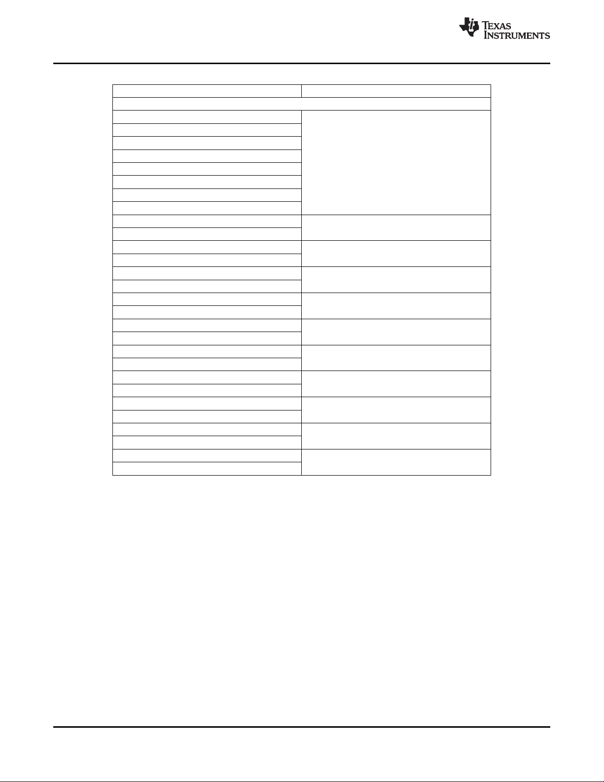
PIN DESCRIPTIONS (SOT-23)
1 V
IN
2 GND Ground pin.
3 EN Enable pin. The device is in shutdown mode when voltage to this pin is <0.4V and enabled
4 FB Feedback analog input. Connect directly to the output filter capacitor for fixed voltage
5 SW Switching node connection to the internal PFET switch and NFET synchronous rectifier.
Power supply input. Connect to the input filter capacitor (Figure 1).
when >1.0V. Do not leave this pin floating.
versions. For adjustable version external resistor dividers are required (Figure 2). The
internal resistor dividers are disabled for the adjustable version.
PIN DESCRIPTIONS (5-Bump DSBGA)
Pin # Name Description
A1 V
IN
Power supply input. Connect to the input filter capacitor (Figure 1).
A3 GND Ground pin.
C1 EN Enable pin. The device is in shutdown mode when voltage to this pin is <0.4V and enabled
when >1.0V. Do not leave this pin floating.
C3 FB Feedback analog input. Connect directly to the output filter capacitor for fixed voltage
versions. For adjustable version external resistor dividers are required (Figure 2). The
internal resistor dividers are disabled for the adjustable version.
B2 SW Switching node connection to the internal PFET switch and NFET synchronous rectifier.
PIN DESCRIPTIONS (6-Pin USON)
Pin # Name Description
1 EN Enable pin. The device is in shutdown mode when voltage to this pin is <0.4V and enabled
2 Pgnd Ground pin.
3 V
IN
4 SW Switching node connection to the internal PFET switch and NFET synchronous rectifier.
5 Sgnd Singnal ground (feedback ground).
6 FB Feedback analog input. Connect directly to the output filter capacitor for fixed voltage
These devices have limited built-in ESD protection. The leads should be shorted together or the device placed in conductive foam
during storage or handling to prevent electrostatic damage to the MOS gates.
when >1.0V. Do not leave this pin floating.
Power supply input. Connect to the input filter capacitor (Figure 1).
versions. For adjustable version external resistor dividers are required (Figure 2). The
internal resistor dividers are disabled for the adjustable version.
Copyright © 2004–2013, Texas Instruments Incorporated Submit Documentation Feedback 3
Product Folder Links: LM3671 LM3671Q
LM3671
LM3671Q
SNVS294P –NOVEMBER 2004–REVISED MAY 2013
Orderable Voltage Option (V)
SOT-23 Package
LM3671MF-1.2
LM3671MFX-1.2
LM3671MF-1.2/NOPB
LM3671MFX-1.2/NOPB
LM3671QMF-1.2
LM3671QMFX-1.2
LM3671QMF-1.2/NOPB
LM3671QMFX-1.2/NOPB
LM3671MF-1.25/NOPB
LM3671MFX-1.25/NOPB
LM3671MF-1.375/NOPB
LM3671MFX-1.375/NOPB
LM3671MF-1.5/NOPB
LM3671MFX-1.5/NOPB
LM3671MF-1.6/NOPB
LM3671MFX-1.6/NOPB
LM3671MF-1.8/NOPB
LM3671MFX-1.8/NOPB
LM3671MF-1.875/NOPB
LM3671MFX-1.875/NOPB
LM3671MF-2.5/NOPB
LM3671MFX-2.5/NOPB
LM3671MF-2.8/NOPB
LM3671MFX-2.8/NOPB
LM3671MF-3.3/NOPB
LM3671MFX-3.3/NOPB
LM3671MF-ADJ/NOPB
LM3671MFX-ADJ/NOPB
(1) For the most current package and ordering information, see the Package Option Addendum at the end
of this document, or see the TI web site at www.ti.com.
(2) Package drawings, thermal data, and symbolization are available at www.ti.com/packaging.
ORDERING INFORMATION
www.ti.com
(1)(2)
1.2
1.25
1.375
1.5
1.6
1.8
1.875
2.5
2.8
3.3
Adjustable
4 Submit Documentation Feedback Copyright © 2004–2013, Texas Instruments Incorporated
Product Folder Links: LM3671 LM3671Q

www.ti.com
DSBGA Package
LM3671TL-1.2/NOPB
LM3671TLX-1.2/NOPB
LM3671TL-1.25/NOPB
LM3671TLX-1.25/NOPB
LM3671TL-1.5/NOPB
LM3671TLX-1.5/NOPB
LM3671TL-1.8/NOPB
LM3671TLX-1.8/NOPB
LM3671TL-1.875/NOPB
LM3671TLX-1.875/NOPB
LM3671TL-2.5/NOPB
LM3671TLX-2.5/NOPB
LM3671TL-2.8/NOPB
LM3671TLX-2.8/NOPB
LM3671TL-3.3/NOPB
LM3671TLX-3.3/NOPB
LM3671TL-ADJ/NOPB
LM3671TLX-ADJ/NOPB
USON Package
LM3671LC-1.2/NOPB
LM3671LCX-1.2/NOPB
LM3671LC-1.3/NOPB
LM3671LCX-1.3/NOPB
LM3671LC-1.6/NOPB
LM3671LCX-1.6/NOPB
LM3671LC-1.8/NOPB
LM3671LCX-1.8/NOPB
SNVS294P –NOVEMBER 2004–REVISED MAY 2013
ORDERING INFORMATION
Orderable Voltage Option (V)
(1)(2)
(continued)
1.2
1.25
1.5
1.8
1.875
2.5
2.8
3.3
Adjustable
1.2
1.3
1.6
1.8
LM3671
LM3671Q
Copyright © 2004–2013, Texas Instruments Incorporated Submit Documentation Feedback 5
Product Folder Links: LM3671 LM3671Q
LM3671
LM3671Q
SNVS294P –NOVEMBER 2004–REVISED MAY 2013
ABSOLUTE MAXIMUM RATINGS
(1)(2)
VINPin: Voltage to GND −0.2V to 6.0V
FB, SW, EN Pin: (GND−0.2V) to
Continuous Power Dissipation
Junction Temperature (T
(3)
) +125°C
J-MAX
Storage Temperature Range −65°C to +150°C
Maximum Lead Temperature 260°C
(Soldering, 10 sec.)
ESD Rating
(4)
Human Body Model 2 kV
Machine Model 200V
(1) Absolute Maximum Ratings indicate limits beyond which damage to the device may occur. Operating Ratings are conditions under
which operation of the device is specified. Operating Ratings do not imply specified performance limits. For specified performance limits
and associated test conditions, see the Electrical Characteristics tables.
(2) If Military/Aerospace specified devices are required, please contact the Texas Instruments Sales Office / Distributors for
availability and specifications.
(3) Internal thermal shutdown circuitry protects the device from permanent damage. Thermal shutdown engages at TJ= 150°C (typ.) and
disengages at TJ= 130°C (typ.).
(4) The Human body model is a 100 pF capacitor discharged through a 1.5 kΩ resistor into each pin. The machine model is a 200 pF
capacitor discharged directly into each pin. MIL-STD-883 3015.7
www.ti.com
(VIN+ 0.2V)
Internally Limited
OPERATING RATINGS
Input Voltage Range
(3)
(1) (2)
2.7V to 5.5V
Recommended Load Current 0mA to 600 mA
Junction Temperature (TJ) Range −40°C to +125°C
Ambient Temperature (TA) Range
(4)
−40°C to +85°C
(1) Absolute Maximum Ratings indicate limits beyond which damage to the device may occur. Operating Ratings are conditions under
which operation of the device is specified. Operating Ratings do not imply specified performance limits. For specified performance limits
and associated test conditions, see the Electrical Characteristics tables.
(2) All voltages are with respect to the potential at the GND pin.
(3) The input voltage range recommended for ideal applications performance for the specified output voltages are given below:VIN= 2.7V to
4.5V for 1.1V ≤ V
V
DROPOUT
(4) In Applications where high power dissipation and/or poor package resistance is present, the maximum ambient temperature may have
= I
to be derated. Maximum ambient temperature (T
maximum power dissipation of the device in the application (P
in the application, as given by the following equation:T
different ambient temperatures.
< 1.5VVIN= 2.7V to 5.5V for 1.5V ≤ V
OUT
LOAD
*( R
DSON, PFET
+ R
INDUCTOR
< 1.8VVIN= (V
)
A-MAX
OUT
) is dependent on the maximum operating junction temperature (T
) and the junction to ambient thermal resistance of the package (θJA)
D-MAX
= T
A-MAX
J-MAX
− (θJAx P
+ V
OUT
). Refer to Dissipation rating table for P
D-MAX
DROPOUT
) to 5.5V for 1.8V ≤ V
≤ 3.3Vwhere
OUT
J-MAX
D-MAX
), the
values at
THERMAL PROPERTIES
Junction-to-Ambient Thermal Resistance (θJA) (SOT-23) for 4-layer board
Junction-to-Ambient Thermal Resistance (θJA) (DSBGA) for 4-layer board
Junction-to-Ambient Thermal Resistance (θJA) (USON) for 4-layer board
(1) Junction to ambient thermal resistance is highly application and board layout dependent. In applications where high power dissipation
exists, special care must be given to thermal dissipation issues in board design. Specified value of 130 °C/W for SOT-23 is based on a 4
layer, 4" x 3", 2/1/1/2 oz. Cu board as per JEDEC standards is used.
(1)
(1)
(1)
130°C/W
85°C/W
165°C/W
6 Submit Documentation Feedback Copyright © 2004–2013, Texas Instruments Incorporated
Product Folder Links: LM3671 LM3671Q
LM3671
LM3671Q
www.ti.com
ELECTRICAL CHARACTERISTICS
(1)(2)(3)
Limits in standard typeface are for TJ= 25°C. Limits in boldface type apply over the entire junction temperature range for
operation, −40°C to +125°C. Unless otherwise noted, specifications apply to the LM3671MF/TL/LC with VIN= EN = 3.6V
Symbol Parameter Condition Min Typ Max Units
V
IN
Input Voltage
Feedback Voltage (Fixed) MF −4 +4
Feedback Voltage (Fixed) TL PWM mode
Feedback Voltage (Fixed) LC −4 +4
Feedback Voltage (ADJ) MF
V
FB
(6)
Feedback Voltage (ADJ) TL −2.5 +2.5
Line Regulation 0.031 %/V
Load Regulation 0.0013 %/mA
V
REF
I
SHDN
I
Q
R
DSON (P)
R
DSON (N)
I
LIM
V
IH
V
IL
I
EN
F
OSC
Internal Reference Voltage 0.5 V
Shutdown Supply Current EN = 0V 0.01 1 µA
DC Bias Current into V
IN
Pin-Pin Resistance for PFET VIN= VGS= 3.6V 380 500 mΩ
Pin-Pin Resistance for NFET VIN= VGS= 3.6V 250 400 mΩ
Switch Peak Current Limit Open Loop
Logic High Input 1.0 V
Logic Low Input 0.4 V
Enable (EN) Input Current 0.01 1 µA
Internal Oscillator Frequency PWM Mode
(1) All voltages are with respect to the potential at the GND pin.
(2) Min and Max limits are specified by design, test or statistical analysis. Typical numbers are not specified, but do represent the most
likely norm.
(3) The parameters in the electrical characteristic table are tested at VIN= 3.6V unless otherwise specified. For performance over the input
voltage range refer to datasheet curves.
(4) The input voltage range recommended for ideal applications performance for the specified output voltages are given below:VIN= 2.7V to
4.5V for 1.1V ≤ V
V
DROPOUT
(5) Test condition: for V
= I
(6) ADJ version is configured to 1.5V output. For ADJ output version: VIN= 2.7V to 4.5V for 0.90V ≤ V
≤ V
< 3.3V
OUT
(7) Refer to datasheet curves for closed loop data and its variation with regards to supply voltage and temperature. Electrical Characteristic
< 1.5VVIN= 2.7V to 5.5V for 1.5V ≤ V
OUT
LOAD
*( R
DSON, PFET
less than 2.5V, VIN= 3.6V; for V
OUT
+ R
INDUCTOR
)
table reflects open loop data (FB=0V and current drawn from SW pin ramped up until cycle by cycle current limit is activated). Closed
loop current limit is the peak inductor current measured in the application circuit by increasing output current until output voltage drops
by 10%.
(4)
(5)
PWM mode
(5)
2.7V ≤ VIN≤ 5.5V
IO= 10 mA
100 mA ≤ IO≤ 600 mA
VIN= 3.6V
No load, device is not switching (FB
forced higher than programmed 16 35 µA
output voltage)
(7)
(5)
< 1.8VVIN= (V
OUT
greater than or equal to 2.5V, VIN= V
OUT
OUT
SNVS294P –NOVEMBER 2004–REVISED MAY 2013
2.7 5.5 V
−2.5 +2.5 %
−4 +4
830 1020 1150 mA
1.6 2 2.6 MHz
+ V
DROPOUT
) to 5.5V for 1.8V ≤ V
+ 1V.
OUT
< 1.1VVIN= 2.7V to 5.5V for 1.1V
OUT
≤ 3.3Vwhere
OUT
%
DISSIPATION RATING TABLE
θ
JA
130°C/W (4 layer board) SOT-23 770 mW 500 mW 310 mW
85°C/W (4 layer board) 5-bump 1179 mW 765 mW 470 mW
DSBGA
165°C/W (4 layer board) 6-pin 606 mW 394 mW 242 mW
USON
Copyright © 2004–2013, Texas Instruments Incorporated Submit Documentation Feedback 7
TA≤ 25°C TA= 60°C TA= 85°C
Power Rating Power Rating Power Rating
Product Folder Links: LM3671 LM3671Q
2 MHz
Oscillator
Soft
Start
Ramp
Generator
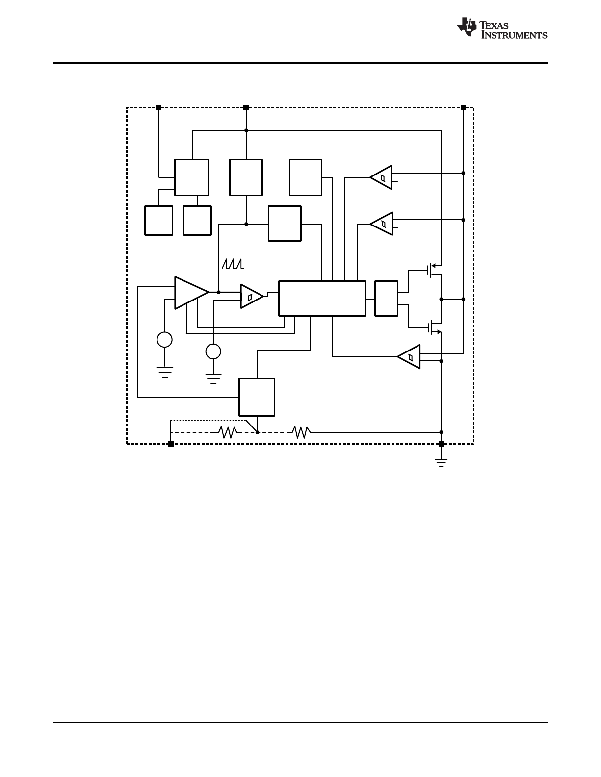
Thermal
Shutdown
Undervoltage
Lockout
Frequency
Compensation
+
-
Error
Amp
Control Logic Driver
Current Limit
Comparator
Ref1
PFM Current
Comparator
Ref2
SW
Zero Crossing
Comparator
FB
EN
V
IN
PWM Comparator
pfm_low
pfm_hi
GND
Bandgap
+
-
Vcomp
1.0V
Fixed Ver
Adj Ver
+
-
0.5V
+
-
+
-
+
-
V
REF
LM3671
LM3671Q
SNVS294P –NOVEMBER 2004–REVISED MAY 2013
BLOCK DIAGRAM
www.ti.com
8 Submit Documentation Feedback Copyright © 2004–2013, Texas Instruments Incorporated
Figure 6. Simplified Functional Diagram
Product Folder Links: LM3671 LM3671Q
-10 10 30 50 70 90 110
TEMPERATURE (oC)
100
150
200
250
300
350
400
450
500
550
600
R
DS(ON)
(m:)
-30
NFET
VIN = 4.5V
PFET
VIN = 2.7V
VIN = 4.5V
VIN = 3.6V
VIN = 3.6V
VIN = 2.7V
3.0 3.5 4.0 4.5 5.0 5.5 6.0
SUPPLY VOLTAGE (V)
10
12
14
16
18
20
QUIESCENT CURRENT (P
A
)
2.5
TA = 85°C
EN = V
IN
I
OUT
= 0 mA
TA = 25°C
TA = -30°C
-10 10 30 50 70 90
TEMPERATURE (°C)
0.00
0.05
0.10
0.15
0.20
0.25
0.30
0.35
0.40
SHUTDOWN CURRENT (PA)
-30
EN = GND
VIN = 3.6V
VIN = 2.7V
VIN = 5.5V
www.ti.com
SNVS294P –NOVEMBER 2004–REVISED MAY 2013
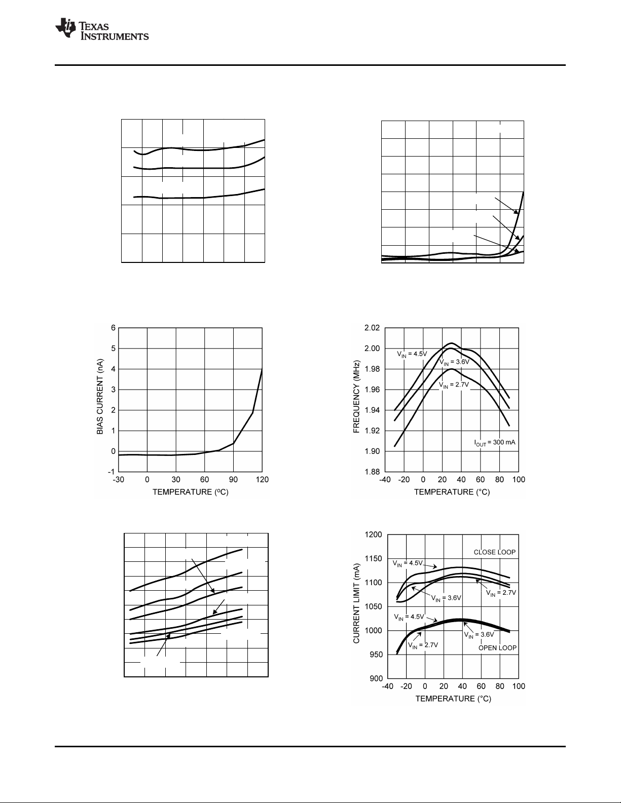
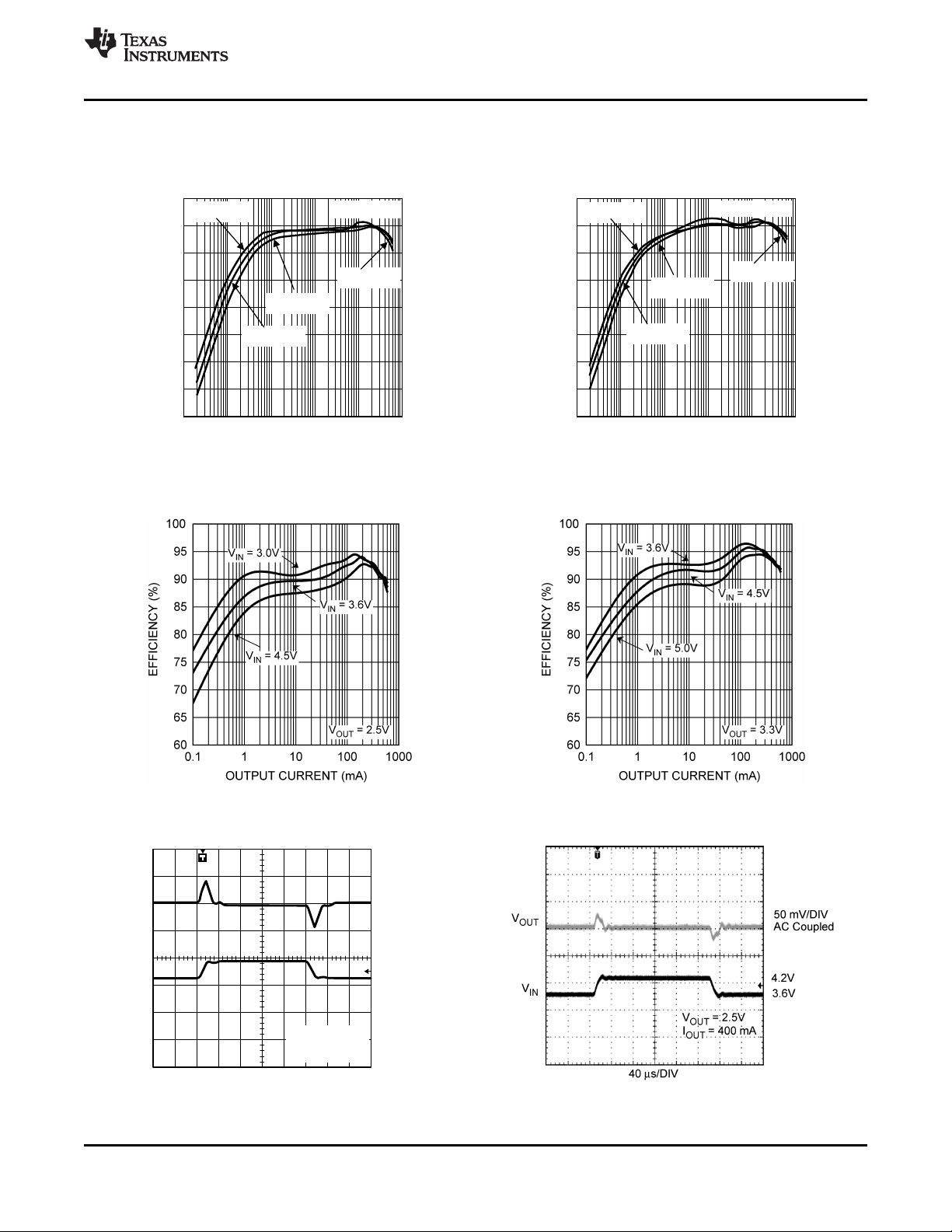
TYPICAL PERFORMANCE CHARACTERISTICS
LM3671MF/TL/LC, Circuit of Figure 1, VIN= 3.6V, V
Quiescent Supply Current vs. Supply Voltage Shutdown Current vs. Temp
Figure 7. Figure 8.
Feedback Bias Current vs. Temp Switching Frequency vs. Temperature
= 1.5V, TA= 25°C, unless otherwise noted.
OUT
LM3671
LM3671Q
Figure 9. Figure 10.
R
vs. Temperature Open/Closed Loop Current Limit vs. Temperature
DS(ON)
Copyright © 2004–2013, Texas Instruments Incorporated Submit Documentation Feedback 9
Figure 11. Figure 12.
Product Folder Links: LM3671 LM3671Q
0 100 200 300 400 500 600
OUTPUT CURRENT (mA)
1.48
1.5
1.52
1.54
OUTPUT VOLTAGE (V)
VIN = 3.6V
V
OUT
= 1.5V
PFM Mode
PWM Mode
-10 10 30 50 70 90
TEMPERATURE (oC)
1.4800
1.4850
1.4900
1.4950
1.5000
1.5050
1.5100
1.5150
1.5200
1.5250
1.5300
OUTPUT VOLTAGE (V)
-30
PFM Mode
PWM Mode
I
OUT
= 300 mA
VIN = 3.6V
V
OUT
= 1.5V
I
OUT
= 600 mA
I
OUT
= 10 mA
2.5 3 3.5 4 4.5 5 5.5
SUPPLY VOLTAGE(V)
1.4800
1.4900
1.5000
1.5100
1.5200
1.5300
= 10 mAI
OUT
= 1.5 V
OUT
V
= 300 mA
I
OUT
= 500 mA
I
OUT
= 600 mA
I
OUT
OUTPUT VOLTAGE (V)
LM3671
LM3671Q
SNVS294P –NOVEMBER 2004–REVISED MAY 2013
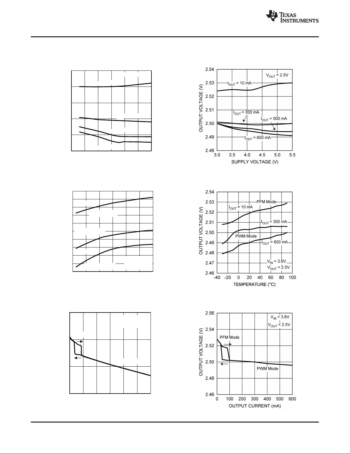
TYPICAL PERFORMANCE CHARACTERISTICS (continued)
LM3671MF/TL/LC, Circuit of Figure 1, VIN= 3.6V, V
Output Voltage vs. Supply Voltage Output Voltage vs. Supply Voltage
(V
= 1.5V) (V
OUT
Figure 13. Figure 14.
= 1.5V, TA= 25°C, unless otherwise noted.
OUT
OUT
www.ti.com
= 2.5V)
Output Voltage vs. Temperature Output Voltage vs. Temperature
(V
= 1.5V) (V
OUT
OUT
= 2.5V)
Figure 15. Figure 16.
Output Voltage vs. Output Current Output Voltage vs. Output Current
(V
= 1.5V) (V
OUT
OUT
= 2.5V)
10 Submit Documentation Feedback Copyright © 2004–2013, Texas Instruments Incorporated
Figure 17. Figure 18.
Product Folder Links: LM3671 LM3671Q
V
OUT
40 Ps/DIV
3.6V
V
IN
3.0V
20 mV/DIV
AC Coupled
V
OUT
= 1.5V
I
OUT
= 400 mA
0.10 1.00 10.00 100.00 1000.00
OUTPUT CURRENT (mA)
20
30
40
50
60
70
80
90
100
EFFICIENCY (%)
0.01
VIN = 2.7V
VIN = 2.7V
VIN = 4.5V
VIN = 3.6V
V
OUT
= 1.5V
0.10 1.00 10.00 100.00 1000.00
OUTPUT CURRENT (mA)
20
30
40
50
60
70
80
90
100
EFFICIENCY (%)
0.01
VIN = 3.0V
VIN = 3.0V
VIN = 4.5V
VIN = 3.6V
V
OUT
= 1.8V
www.ti.com
TYPICAL PERFORMANCE CHARACTERISTICS (continued)
LM3671MF/TL/LC, Circuit of Figure 1, VIN= 3.6V, V
Efficiency vs. Output Current Efficiency vs. Output Current
(V
= 1.5V, L= 2.2 µH) (V
OUT
Figure 19. Figure 20.
Efficiency vs. Output Current Efficiency vs. Output Current
(V
= 2.5V, L= 2.2 µH) (V
OUT
SNVS294P –NOVEMBER 2004–REVISED MAY 2013
= 1.5V, TA= 25°C, unless otherwise noted.
OUT
OUT
OUT
LM3671
LM3671Q
= 1.8V, L= 2.2 µH)
= 3.3V, L= 2.2 µH)
Figure 21. Figure 22.
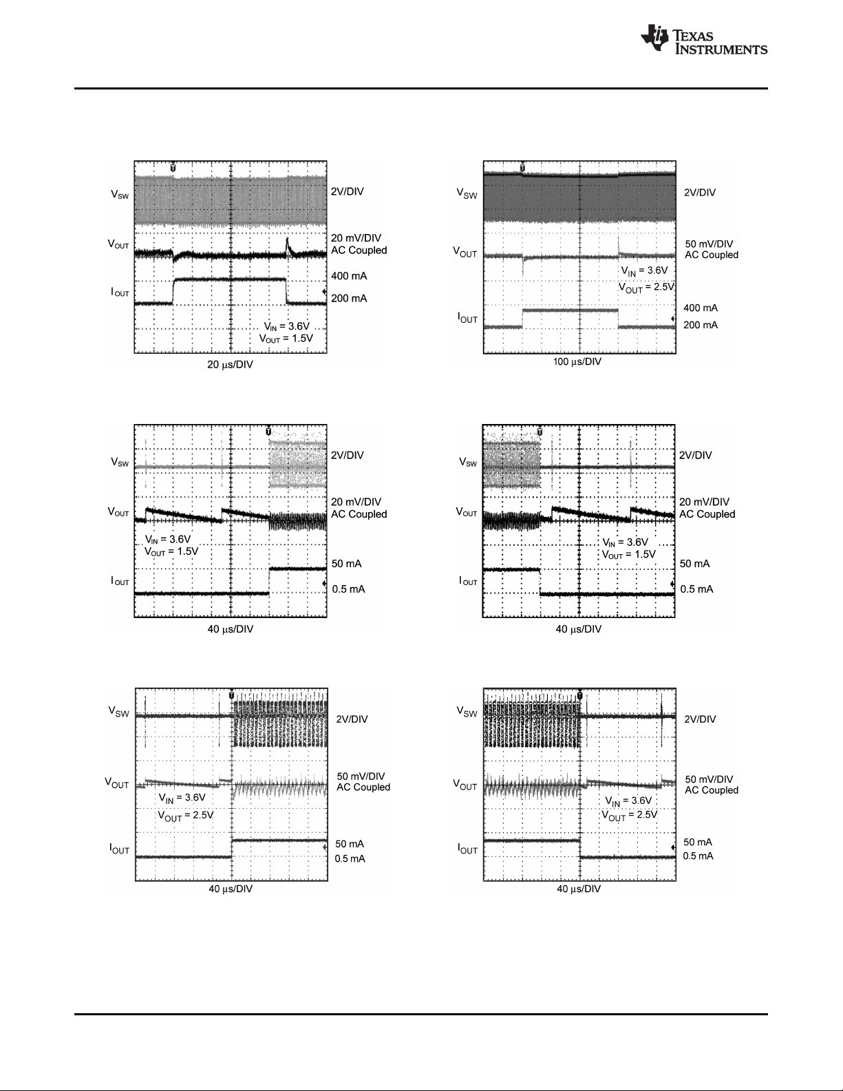
Line Transient Response Line Transient Response
V
= 1.5V (PWM Mode) V
OUT
Figure 23. Figure 24.
Product Folder Links: LM3671 LM3671Q
Copyright © 2004–2013, Texas Instruments Incorporated Submit Documentation Feedback 11
= 2.5V (PWM Mode)
OUT
LM3671
LM3671Q
SNVS294P –NOVEMBER 2004–REVISED MAY 2013
TYPICAL PERFORMANCE CHARACTERISTICS (continued)
LM3671MF/TL/LC, Circuit of Figure 1, VIN= 3.6V, V
Load Transient Response Load Transient Response
V
= 1.5V (PWM Mode) V
OUT
Figure 25. Figure 26.
= 1.5V, TA= 25°C, unless otherwise noted.
OUT
OUT
www.ti.com
= 2.5V (PWM Mode)
Load Transient Response (V
(PFM Mode 0.5 mA to 50 mA) (PFM Mode 50 mA to 0.5 mA)
Figure 27. Figure 28.
Load Transient Response (V
(PFM Mode 0.5 mA to 50 mA) (PFM Mode 50 mA to 0.5 mA)
= 1.5V) Load Transient Response (V
OUT
= 2.5V) Load Transient Response (V
OUT
OUT
OUT
= 1.5V)
= 2.5V)
Figure 29. Figure 30.
12 Submit Documentation Feedback Copyright © 2004–2013, Texas Instruments Incorporated
Product Folder Links: LM3671 LM3671Q

V
OUT
TIME (100 Ps/DIV)
EN
V
SW
2V/DIV
500 mA/DIV
VIN = 3.6V
V
OUT
= 1.5V
2V/DIV
I
OUT
= 300 mA
I
L
1V/DIV
www.ti.com
TYPICAL PERFORMANCE CHARACTERISTICS (continued)
LM3671MF/TL/LC, Circuit of Figure 1, VIN= 3.6V, V
Mode Change by Load Transients Mode Change by Load Transients
V
= 1.5V (PFM to PWM) V
OUT
Figure 31. Figure 32.
Mode Change by Load Transients Mode Change by Load Transients
V
= 2.5V (PFM to PWM) V
OUT
SNVS294P –NOVEMBER 2004–REVISED MAY 2013
= 1.5V, TA= 25°C, unless otherwise noted.
OUT
OUT
OUT
LM3671
LM3671Q
= 1.5V (PWM to PFM)
= 2.5V (PWM to PFM)
Figure 33. Figure 34.
Start Up into PWM Mode Start Up into PWM Mode
V
= 1.5V (Output Current= 300 mA) V
OUT
Figure 35. Figure 36.
Copyright © 2004–2013, Texas Instruments Incorporated Submit Documentation Feedback 13
Product Folder Links: LM3671 LM3671Q
= 2.5V (Output Current= 300 mA)
OUT

V
OUT
TIME (100 Ps/DIV)
EN
V
SW
2V/DIV
500 mV/DIV
VIN = 3.6V
V
OUT
= 1.5V
I
OUT
= 1 mA
2V/DIV
LM3671
LM3671Q
SNVS294P –NOVEMBER 2004–REVISED MAY 2013
TYPICAL PERFORMANCE CHARACTERISTICS (continued)
LM3671MF/TL/LC, Circuit of Figure 1, VIN= 3.6V, V
Start Up into PFM Mode Start Up into PFM Mode
V
= 1.5V (Output Current= 1mA) V
OUT
Figure 37. Figure 38.
= 1.5V, TA= 25°C, unless otherwise noted.
OUT
= 2.5V (Output Current= 1mA)
OUT
www.ti.com
14 Submit Documentation Feedback Copyright © 2004–2013, Texas Instruments Incorporated
Product Folder Links: LM3671 LM3671Q

LM3671
LM3671Q
www.ti.com
OPERATION DESCRIPTION
DEVICE INFORMATION
The LM3671, a high-efficiency step-down DC-DC switching buck converter, delivers a constant voltage from a
single Li-Ion battery and input voltage rails from 2.7V to 5.5V to portable devices such as cell phones and PDAs.
Using a voltage mode architecture with synchronous rectification, the LM3671 has the ability to deliver up to 600
mA depending on the input voltage, output voltage, ambient temperature and the inductor chosen.
There are three modes of operation depending on the current required - PWM (Pulse Width Modulation), PFM
(Pulse Frequency Modulation), and shutdown. The device operates in PWM mode at load current of
approximately 80 mA or higher. Lighter load current cause the device to automatically switch into PFM for
reduced current consumption (IQ= 16 µA typ) and a longer battery life. Shutdown mode turns off the device,
offering the lowest current consumption (I
SHUTDOWN
= 0.01 µA typ).
Additional features include soft-start, under-voltage protection, current overload protection, and thermal shutdown
protection. As shown in Figure 1, only three external power components are required for implementation.
The part uses an internal reference voltage of 0.5V. It is recommended to keep the part in shutdown until the
input voltage is 2.7V or higher.
CIRCUIT OPERATION
During the first portion of each switching cycle, the control block in the LM3671 turns on the internal PFET
switch. This allows current to flow from the input through the inductor to the output filter capacitor and load. The
inductor limits the current to a ramp with a slope of (VIN–V
During the second portion of each cycle, the controller turns the PFET switch off, blocking current flow from the
input, and then turns the NFET synchronous rectifier on. The inductor draws current from ground through the
NFET to the output filter capacitor and load, which ramps the inductor current down with a slope of - V
The output filter stores charge when the inductor current is high, and releases it when inductor current is low,
smoothing the voltage across the load.
The output voltage is regulated by modulating the PFET switch on time to control the average current sent to the
load. The effect is identical to sending a duty-cycle modulated rectangular wave formed by the switch and
synchronous rectifier at the SW pin to a low-pass filter formed by the inductor and output filter capacitor. The
output voltage is equal to the average voltage at the SW pin.
)/L, by storing energy in a magnetic field.
OUT
SNVS294P –NOVEMBER 2004–REVISED MAY 2013
/L.
OUT
PWM OPERATION
During PWM operation the converter operates as a voltage-mode controller with input voltage feed forward. This
allows the converter to achieve good load and line regulation. The DC gain of the power stage is proportional to
the input voltage. To eliminate this dependence, feed forward inversely proportional to the input voltage is
introduced.
While in PWM mode, the output voltage is regulated by switching at a constant frequency and then modulating
the energy per cycle to control power to the load. At the beginning of each clock cycle the PFET switch is turned
on and the inductor current ramps up until the comparator trips and the control logic turns off the switch. The
current limit comparator can also turn off the switch in case the current limit of the PFET is exceeded. Then the
NFET switch is turned on and the inductor current ramps down. The next cycle is initiated by the clock turning off
the NFET and turning on the PFET.
Copyright © 2004–2013, Texas Instruments Incorporated Submit Documentation Feedback 15
Product Folder Links: LM3671 LM3671Q

V
OUT
TIME (4 Ps/DIV)
200 mA/DIV
I
L
V
SW
2V/DIV
20 mV/DIV
AC Coupled
VIN = 3.6V
V
OUT
= 1.5V
I
OUT
= 20 mA
V
OUT
TIME (200 ns/DIV)
200 mA/DIV
I
L
V
SW
2V/DIV
10 mV/DIV
AC Coupled
VIN = 3.6V
V
OUT
= 1.5V
I
OUT
= 400 mA
LM3671
LM3671Q
SNVS294P –NOVEMBER 2004–REVISED MAY 2013
Figure 39. Typical PWM Operation
Internal Synchronous Rectification
While in PWM mode, the LM3671 uses an internal NFET as a synchronous rectifier to reduce rectifier forward
voltage drop and associated power loss. Synchronous rectification provides a significant improvement in
efficiency whenever the output voltage is relatively low compared to the voltage drop across an ordinary rectifier
diode.
www.ti.com
Current Limiting
A current limit feature allows the LM3671 to protect itself and external components during overload conditions.
PWM mode implements current limiting using an internal comparator that trips at 1020 mA (typ.). If the output is
shorted to ground the device enters a timed current limit mode where the NFET is turned on for a longer duration
until the inductor current falls below a low threshold. This allows the inductor current more time to decay, thereby
preventing runaway.
PFM OPERATION
At very light load, the converter enters PFM mode and operates with reduced switching frequency and supply
current to maintain high efficiency.
The part automatically transitions into PFM mode when either of two conditions occurs for a duration of 32 or
more clock cycles:
A. The NFET current reaches zero.
B. The peak PMOS switch current drops below the I
level, (Typically I
MODE
< 30 mA + VIN/42Ω ).
MODE
Figure 40. Typical PFM Operation
16 Submit Documentation Feedback Copyright © 2004–2013, Texas Instruments Incorporated
Product Folder Links: LM3671 LM3671Q

High PFM Threshold
~1.017*Vout
Low1 PFM Threshold
~1.006*Vout
PFM Mode at Light Load
PWM Mode at
Moderate to Heavy
Loads
Pfet on
until
Ipfm limit
reached
Nfet on
drains
inductor
current
until
I inductor = 0
High PFM
Voltage
Threshold
reached,
go into
sleep mode
Low PFM
Threshold,
turn on
PFET
Current load
increases,
draws Vout
towards
Low2 PFM
Threshold
Low2 PFM Threshold,
switch back to PWMmode
Load current
increases
Low2 PFM Threshold
Vout
Z-
A
xi
s
Z
-
Axis
LM3671
LM3671Q
www.ti.com
During PFM operation, the converter positions the output voltage slightly higher than the nominal output voltage
during PWM operation, allowing additional headroom for voltage drop during a load transient from light to heavy
load. The PFM comparators sense the output voltage via the feedback pin and control the switching of the output
FETs such that the output voltage ramps between ~0.6% and ~1.7% above the nominal PWM output voltage. If
the output voltage is below the ‘high’ PFM comparator threshold, the PMOS power switch is turned on. It remains
on until the output voltage reaches the ‘high’ PFM threshold or the peak current exceeds the I
PFM mode. The typical peak current in PFM mode is: I
= 112 mA + VIN/27Ω .
PFM
Once the PMOS power switch is turned off, the NMOS power switch is turned on until the inductor current ramps
to zero. When the NMOS zero-current condition is detected, the NMOS power switch is turned off. If the output
voltage is below the ‘high’ PFM comparator threshold (see Figure 41), the PMOS switch is again turned on and
the cycle is repeated until the output reaches the desired level. Once the output reaches the ‘high’ PFM
threshold, the NMOS switch is turned on briefly to ramp the inductor current to zero and then both output
switches are turned off and the part enters an extremely low power mode. Quiescent supply current during this
‘sleep’ mode is 16 µA (typ.), which allows the part to achieve high efficiency under extremely light load
conditions.
If the load current should increase during PFM mode (see Figure 41) causing the output voltage to fall below the
‘low2’ PFM threshold, the part will automatically transition into fixed-frequency PWM mode. When VIN=2.7V the
part transitions from PWM to PFM mode at ~35 mA output current and from PFM to PWM mode at ~85 mA ,
when VIN=3.6V, PWM to PFM transition happens at ~50 mA and PFM to PWM transition happens at ~100 mA,
when VIN=4.5V, PWM to PFM transition happens at ~65 mA and PFM to PWM transition happens at ~115 mA.
SNVS294P –NOVEMBER 2004–REVISED MAY 2013
level set for
PFM
Figure 41. Operation in PFM Mode and Transfer to PWM Mode
SHUTDOWN MODE
Setting the EN input pin low (<0.4V) places the LM3671 in shutdown mode. During shutdown the PFET switch,
NFET switch, reference, control and bias circuitry of the LM3671 are turned off. Setting EN high (>1.0V) enables
normal operation. It is recommended to set EN pin low to turn off the LM3671 during system power up and
undervoltage conditions when the supply is less than 2.7V. Do not leave the EN pin floating.
SOFT START
The LM3671 has a soft-start circuit that limits in-rush current during startup. During startup the switch current limit
is increased in steps. Soft start is activated only if EN goes from logic low to logic high after Vin reaches 2.7V.
Soft start is implemented by increasing switch current limit in steps of 70 mA, 140 mA, 280 mA and 1020 mA
(typical switch current limit). The startup time thereby depends on the output capacitor and load current
demanded at startup. Typical startup times with a 10 µF output capacitor and 300 mA load is 400 µs and with
1mA load is 275 µs.
Copyright © 2004–2013, Texas Instruments Incorporated Submit Documentation Feedback 17
Product Folder Links: LM3671 LM3671Q

LM3671
LM3671Q
SNVS294P –NOVEMBER 2004–REVISED MAY 2013
LDO - LOW DROPOUT OPERATION
The LM3671-ADJ can operate at 100% duty cycle (no switching; PMOS switch completely on) for low dropout
support of the output voltage. In this way the output voltage will be controlled down to the lowest possible input
voltage. When the device operates near 100% duty cycle, output voltage ripple is approximately 25 mV.
The minimum input voltage needed to support the output voltage is
V
= I
IN, MIN
where
* (R
LOAD
• I
LOAD: Load current
• R
DSON, PFET: Drain to source resistance of PFET switch in the triode region
• R
INDUCTOR: Inductor resistance
DSON, PFET
+ R
INDUCTOR
) + V
OUT
www.ti.com
(1)
18 Submit Documentation Feedback Copyright © 2004–2013, Texas Instruments Incorporated
Product Folder Links: LM3671 LM3671Q

Fp =
1
2 * S * (R1 R2) * (C1+C2)
Fz =
1
(2 * S * R1 * C1)
C2 =
1
(2 * S * R2 * 45 kHz)
C1 =
1
(2 * S * R1 * 45 kHz)
V
OUT
= V
FB
1 +
R1
R2
¹
·
©
§
LM3671
LM3671Q
www.ti.com
APPLICATION INFORMATION
OUTPUT VOLTAGE SELECTION FOR LM3671-ADJ
The output voltage of the adjustable parts can be programmed through the resistor network connected from V
to FB, then to GND. V
should be 200 kΩ to keep the current drawn through this network well below the 16 µA quiescent current level
(PFM mode) but large enough that it is not susceptible to noise. If R2 is 200 kΩ, and VFBis 0.5V, the current
through the resistor feedback network will be 2.5 µA. The output voltage of the adjustable parts ranges from 1.1V
to 3.3V.
The formula for output voltage selection is:
where
• V
• VFB: feedback voltage = 0.5V
• R1: feedback resistor from V
• R2: feedback resistor from FB to GND (2)
: output voltage (volts)
OUT
For any output voltage greater than or equal to 1.1V, a zero must be added around 45 kHz for stability. The
formula for calculation of C1 is:
is adjusted to make the voltage at FB equal to 0.5V. The resistor from FB to GND (R2)
OUT
to FB
OUT
SNVS294P –NOVEMBER 2004–REVISED MAY 2013
OUT
(3)
For output voltages higher than 2.5V, a pole must be placed at 45 kHz as well. If the pole and zero are at the
same frequency the formula for calculation of C2 is:
(4)
The formula for location of zero and pole frequency created by adding C1 and C2 is given below. By adding C1,
a zero as well as a higher frequency pole is introduced.
(5)
(6)
See the "LM3671-ADJ configurations for various V
Table 1. LM3671-ADJ Configurations For Various V
OUT
" table.
(Circuit of Figure 2)
OUT
(Refer to Note 11 for VIN requirements)
V
(V) R1(kΩ) R2 (kΩ) C1 (pF) C2 (pF) L (µH) CIN(µF) C
OUT
0.90 160 200 22 none 2.2 4.7 10
1.1 240 200 15 none 2.2 4.7 10
1.2 280 200 12 none 2.2 4.7 10
1.3 320 200 12 none 2.2 4.7 10
1.5 357 178 10 none 2.2 4.7 10
1.6 442 200 8.2 none 2.2 4.7 10
1.7 432 178 8.2 none 2.2 4.7 10
1.8 464 178 8.2 none 2.2 4.7 10
1.875 523 191 6.8 none 2.2 4.7 10
2.5 402 100 8.2 none 2.2 4.7 10
2.8 464 100 8.2 33 2.2 4.7 10
3.3 562 100 6.8 33 2.2 4.7 10
OUT
(µF)
Copyright © 2004–2013, Texas Instruments Incorporated Submit Documentation Feedback 19
Product Folder Links: LM3671 LM3671Q

I
RMS
= I
OUTMAX
The worst case is when VIN = 2 V
OUT
(VIN - V
OUT
) V
OUT
L f I
OUTMAX
V
IN
r =
V
OUT
V
IN
r
2
12
1 -
+
V
OUT
V
IN
¸
¸
¹
·
¨
¨
©
§
¸
¹
·
¨
©
§
f
1
L2
!
I
SAT
I
OUTMAX
+ I
RIPPLE
where I
RIPPLE
=
V
OUT
V
IN
¸
¹
·
¨
©
§
¸
¹
·
¨
©
§
VIN - V
OUT
LM3671
LM3671Q
SNVS294P –NOVEMBER 2004–REVISED MAY 2013
INDUCTOR SELECTION
There are two main considerations when choosing an inductor; the inductor should not saturate, and the inductor
current ripple should be small enough to achieve the desired output voltage ripple. Different saturation current
rating specifications are followed by different manufacturers so attention must be given to details. Saturation
current ratings are typically specified at 25°C. However, ratings at the maximum ambient temperature of
application should be requested from the manufacturer. The minimum value of inductance to specify good
performance is 1.76 µH at I
radiate less noise and should be preferred.
There are two methods to choose the inductor saturation current rating.
Method 1:
The saturation current should be greater than the sum of the maximum load current and the worst case average
to peak inductor current. This can be written as
where
• I
• I
• VIN: maximum input voltage in application
• L : min inductor value including worst case tolerances (30% drop can be considered for method 1)
• f : minimum switching frequency (1.6 Mhz)
• V
: average to peak inductor current
RIPPLE
: maximum load current (600 mA)
OUTMAX
: output voltage (7)
OUT
Method 2:
A more conservative and recommended approach is to choose an inductor that has a saturation current rating
greater than the maximum current limit of 1150mA.
A 2.2 µH inductor with a saturation current rating of at least 1150 mA is recommended for most applications. The
inductor’s resistance should be less than 0.3Ω for good efficiency. Table 2 lists suggested inductors and
suppliers. For low-cost applications, an unshielded bobbin inductor could be considered. For noise critical
applications, a toroidal or shielded-bobbin inductor should be used. A good practice is to lay out the board with
overlapping footprints of both types for design flexibility. This allows substitution of a low-noise shielded inductor,
in the event that noise from low-cost bobbin models is unacceptable.
(typ.) dc current over the ambient temperature range. Shielded inductors
LIM
www.ti.com
INPUT CAPACITOR SELECTION
A ceramic input capacitor of 4.7 µF, 6.3V is sufficient for most applications. Place the input capacitor as close as
possible to the VINpin of the device. A larger value may be used for improved input voltage filtering. Use X7R or
X5R types; do not use Y5V. DC bias characteristics of ceramic capacitors must be considered when selecting
case sizes like 0805 and 0603. The minimum input capacitance to specify good performance is 2.2µF at 3V
dc bias; 1.5µF at 5V dc bias including tolerances and over ambient temperature range. The input filter
capacitor supplies current to the PFET switch of the LM3671 in the first half of each cycle and reduces voltage
ripple imposed on the input power source. A ceramic capacitor’s low ESR provides the best noise filtering of the
input voltage spikes due to this rapidly changing current. Select a capacitor with sufficient ripple current rating.
The input current ripple can be calculated as:
20 Submit Documentation Feedback Copyright © 2004–2013, Texas Instruments Incorporated
Product Folder Links: LM3671 LM3671Q
(8)

V
PP-RMS
= V
PP-C
2
+ V
PP-ESR
2
V
PP-C
=
4*f*C
I
RIPPLE
LM3671
LM3671Q
www.ti.com
Table 2. Suggested Inductors and Their Suppliers
Model Vendor Dimensions LxWxH(mm) D.C.R (max)
DO3314-222MX Coilcraft 3.3 x 3.3 x 1.4 200 mΩ
LPO3310-222MX Coilcraft 3.3 x 3.3 x 1.0 150 mΩ
ELL5GM2R2N Panasonic 5.2 x 5.2 x 1.5 53 mΩ
CDRH2D14NP-2R2NC Sumida 3.2 x 3.2 x 1.55 94 mΩ
OUTPUT CAPACITOR SELECTION
A ceramic output capacitor of 10 µF, 6.3V is sufficient for most applications. Use X7R or X5R types; do not use
Y5V. DC bias characteristics of ceramic capacitors must be considered when selecting case sizes like 0805 and
0603. DC bias characteristics vary from manufacturer to manufacturer and dc bias curves should be requested
from them as part of the capacitor selection process.
The minimum output capacitance to specify good performance is 5.75 µF at 1.8V dc bias including
tolerances and over ambient temperature range. The output filter capacitor smoothes out current flow from
the inductor to the load, helps maintain a steady output voltage during transient load changes and reduces
output voltage ripple. These capacitors must be selected with sufficient capacitance and sufficiently low ESR to
perform these functions.
The output voltage ripple is caused by the charging and discharging of the output capacitor and by the R
can be calculated as:
Voltage peak-to-peak ripple due to capacitance can be expressed as follow:
SNVS294P –NOVEMBER 2004–REVISED MAY 2013
and
ESR
(9)
Voltage peak-to-peak ripple due to ESR can be expressed as follow:
V
PP-ESR
= (2 * I
RIPPLE
) * R
ESR
Because these two components are out of phase the rms (root mean squared) value can be used to get an
approximate value of peak-to-peak ripple.
The peak-to-peak ripple voltage, rms value can be expressed as follow:
(10)
Note that the output voltage ripple is dependent on the inductor current ripple and the equivalent series
resistance of the output capacitor (R
The R
is frequency dependent (as well as temperature dependent); make sure the value used for calculations
ESR
ESR
).
is at the switching frequency of the part.
Table 3. Suggested Capacitors and Their Suppliers
Model Type Vendor Voltage Rating
4.7 µF for C
10 µF for C
IN
C2012X5R0J475K Ceramic, X5R TDK 6.3V 0805 (2012)
JMK212BJ475K Ceramic, X5R Taiyo-Yuden 6.3V 0805 (2012)
GRM21BR60J475K Ceramic, X5R Murata 6.3V 0805 (2012)
C1608X5R0J475K Ceramic, X5R TDK 6.3V 0603 (1608)
OUT
GRM21BR60J106K Ceramic, X5R Murata 6.3V 0805 (2012)
JMK212BJ106K Ceramic, X5R Taiyo-Yuden 6.3V 0805 (2012)
C2012X5R0J106K Ceramic, X5R TDK 6.3V 0805 (2012)
C1608X5R0J106K Ceramic, X5R TDK 6.3V 0603 (1608)
Case Size
Inch (mm)
Copyright © 2004–2013, Texas Instruments Incorporated Submit Documentation Feedback 21
Product Folder Links: LM3671 LM3671Q

LM3671
LM3671Q
SNVS294P –NOVEMBER 2004–REVISED MAY 2013
DSBGA PACKAGE ASSEMBLY AND USE
Use of the DSBGA package requires specialized board layout, precision mounting and careful re-flow
techniques, as detailed in Texas Instruments Application Note AN-1112 (Literature Number SNVA009). Refer to
the section "Surface Mount Technology (DSBGA) Assembly Considerations". For best results in assembly,
alignment ordinals on the PC board should be used to facilitate placement of the device. The pad style used with
DSBGA package must be the NSMD (non-solder mask defined) type. This means that the solder-mask opening
is larger than the pad size. This prevents a lip that otherwise forms if the solder-mask and pad overlap, from
holding the device off the surface of the board and interfering with mounting. See Application Note AN-1112
(Literature Number SNVA009) for specific instructions how to do this. The 5-bump package used for LM3671 has
300 micron solder balls and requires 10.82 mils pads for mounting on the circuit board. The trace to each pad
should enter the pad with a 90° entry angle to prevent debris from being caught in deep corners. Initially, the
trace to each pad should be 7 mil wide, for a section approximately 7 mil long or longer, as a thermal relief. Then
each trace should neck up or down to its optimal width. The important criteria is symmetry. This ensures the
solder bumps on the LM3671 re-flow evenly and that the device solders level to the board. In particular, special
attention must be paid to the pads for bumps A1 and A3, because VINand GND are typically connected to large
copper planes, inadequate thermal relief can result in late or inadequate re-flow of these bumps.
The DSBGA package is optimized for the smallest possible size in applications with red or infrared opaque
cases. Because the DSBGA package lacks the plastic encapsulation characteristic of larger devices, it is
vulnerable to light. Backside metallization and/or epoxy coating, along with front-side shading by the printed
circuit board, reduce this sensitivity. However, the package has exposed die edges. In particular, DSBGA
devices are sensitive to light, in the red and infrared range, shining on the package’s exposed die edges.
www.ti.com
BOARD LAYOUT CONSIDERATIONS
PC board layout is an important part of DC-DC converter design. Poor board layout can disrupt the performance
of a DC-DC converter and surrounding circuitry by contributing to EMI, ground bounce, and resistive voltage loss
in the traces. These can send erroneous signals to the DC-DC converter IC, resulting in poor regulation or
instability.
Good layout for the LM3671 can be implemented by following a few simple design rules below. Refer to
Figure 42 for top layer board layout.
1. Place the LM3671, inductor and filter capacitors close together and make the traces short. The traces
between these components carry relatively high switching currents and act as antennas. Following this rule
reduces radiated noise. Special care must be given to place the input filter capacitor very close to the V
and GND pin.
2. Arrange the components so that the switching current loops curl in the same direction. During the first half of
each cycle, current flows from the input filter capacitor through the LM3671 and inductor to the output filter
capacitor and back through ground, forming a current loop. In the second half of each cycle, current is pulled
up from ground through the LM3671 by the inductor to the output filter capacitor and then back through
ground forming a second current loop. Routing these loops so the current curls in the same direction
prevents magnetic field reversal between the two half-cycles and reduces radiated noise.
3. Connect the ground pins of the LM3671 and filter capacitors together using generous component-side
copper fill as a pseudo-ground plane. Then, connect this to the ground-plane (if one is used) with several
vias. This reduces ground-plane noise by preventing the switching currents from circulating through the
ground plane. It also reduces ground bounce at the LM3671 by giving it a low-impedance ground connection.
4. Use wide traces between the power components and for power connections to the DC-DC converter circuit.
This reduces voltage errors caused by resistive losses across the traces.
5. Route noise sensitive traces, such as the voltage feedback path, away from noisy traces between the power
components. The voltage feedback trace must remain close to the LM3671 circuit and should be direct but
should be routed opposite to noisy components. This reduces EMI radiated onto the DC-DC converter’s own
voltage feedback trace. A good approach is to route the feedback trace on another layer and to have a
ground plane between the top layer and layer on which the feedback trace is routed. In the same manner for
the adjustable part it is desired to have the feedback dividers on the bottom layer.
6. Place noise sensitive circuitry, such as radio IF blocks, away from the DC-DC converter, CMOS digital blocks
and other noisy circuitry. Interference with noise-sensitive circuitry in the system can be reduced through
distance.
IN
22 Submit Documentation Feedback Copyright © 2004–2013, Texas Instruments Incorporated
Product Folder Links: LM3671 LM3671Q

LM3671
LM3671Q
www.ti.com
In mobile phones, for example, a common practice is to place the DC-DC converter on one corner of the board,
arrange the CMOS digital circuitry around it (since this also generates noise), and then place sensitive
preamplifiers and IF stages on the diagonally opposing corner. Often, the sensitive circuitry is shielded with a
metal pan and power to it is post-regulated to reduce conducted noise, using low-dropout linear regulators.
SNVS294P –NOVEMBER 2004–REVISED MAY 2013
Figure 42. Top Layer Board Layout For SOT-23
Copyright © 2004–2013, Texas Instruments Incorporated Submit Documentation Feedback 23
Product Folder Links: LM3671 LM3671Q

LM3671
LM3671Q
SNVS294P –NOVEMBER 2004–REVISED MAY 2013
REVISION HISTORY
Changes from Revision O (April 2013) to Revision P Page
• Changed layout of National Data Sheet to TI format .......................................................................................................... 23
www.ti.com
24 Submit Documentation Feedback Copyright © 2004–2013, Texas Instruments Incorporated
Product Folder Links: LM3671 LM3671Q

PACKAGE OPTION ADDENDUM
www.ti.com
PACKAGING INFORMATION
Orderable Device Status
LM3671LC-1.2/NOPB ACTIVE USON NKH 6 1000 Green (RoHS
LM3671LC-1.3/NOPB ACTIVE USON NKH 6 1000 Green (RoHS
LM3671LC-1.6/NOPB ACTIVE USON NKH 6 1000 Green (RoHS
LM3671LC-1.8/NOPB ACTIVE USON NKH 6 1000 Green (RoHS
LM3671LCX-1.2/NOPB ACTIVE USON NKH 6 4500 Green (RoHS
LM3671LCX-1.3/NOPB ACTIVE USON NKH 6 4500 Green (RoHS
LM3671LCX-1.6/NOPB ACTIVE USON NKH 6 4500 Green (RoHS
LM3671LCX-1.8/NOPB ACTIVE USON NKH 6 4500 Green (RoHS
LM3671MF-1.2 ACTIVE SOT-23 DBV 5 1000 TBD Call TI Call TI -30 to 85 SBPB
LM3671MF-1.2/NOPB ACTIVE SOT-23 DBV 5 1000 Green (RoHS
LM3671MF-1.25 ACTIVE SOT-23 DBV 5 1000 TBD Call TI Call TI -30 to 85 SDRB
Package Type Package
(1)
Drawing
Pins Package
Qty
Eco Plan
(2)
& no Sb/Br)
& no Sb/Br)
& no Sb/Br)
& no Sb/Br)
& no Sb/Br)
& no Sb/Br)
& no Sb/Br)
& no Sb/Br)
& no Sb/Br)
Lead/Ball Finish MSL Peak Temp
(3)
CU NIPDAU Level-1-260C-UNLIM S39
CU NIPDAU Level-1-260C-UNLIM S40
CU NIPDAU Level-1-260C-UNLIM S41
CU NIPDAU Level-1-260C-UNLIM S42
CU NIPDAU Level-1-260C-UNLIM S39
CU NIPDAU Level-1-260C-UNLIM S40
CU NIPDAU Level-1-260C-UNLIM S41
CU NIPDAU Level-1-260C-UNLIM S42
CU SN Level-1-260C-UNLIM -30 to 85 SBPB
Op Temp (°C) Top-Side Markings
2-May-2013
Samples
(4)
LM3671MF-1.25/NOPB ACTIVE SOT-23 DBV 5 1000 Green (RoHS
& no Sb/Br)
LM3671MF-1.375 ACTIVE SOT-23 DBV 5 1000 TBD Call TI Call TI -30 to 85 SEDB
LM3671MF-1.375/NOPB ACTIVE SOT-23 DBV 5 1000 Green (RoHS
& no Sb/Br)
LM3671MF-1.5 ACTIVE SOT-23 DBV 5 1000 TBD Call TI Call TI -30 to 85 SBRB
LM3671MF-1.5/NOPB ACTIVE SOT-23 DBV 5 1000 Green (RoHS
& no Sb/Br)
LM3671MF-1.6 ACTIVE SOT-23 DBV 5 1000 TBD Call TI Call TI -30 to 85 SDUB
LM3671MF-1.6/NOPB ACTIVE SOT-23 DBV 5 1000 Green (RoHS
& no Sb/Br)
Addendum-Page 1
CU SN Level-1-260C-UNLIM -30 to 85 SDRB
CU SN Level-1-260C-UNLIM -30 to 85 SEDB
CU SN Level-1-260C-UNLIM -30 to 85 SBRB
CU SN Level-1-260C-UNLIM -30 to 85 SDUB

PACKAGE OPTION ADDENDUM
www.ti.com
Orderable Device Status
Package Type Package
(1)
Drawing
Pins Package
Qty
Eco Plan
(2)
Lead/Ball Finish MSL Peak Temp
(3)
Op Temp (°C) Top-Side Markings
LM3671MF-1.8 ACTIVE SOT-23 DBV 5 1000 TBD Call TI Call TI -30 to 85 SBSB
LM3671MF-1.8/NOPB ACTIVE SOT-23 DBV 5 1000 Green (RoHS
CU SN Level-1-260C-UNLIM -30 to 85 SBSB
& no Sb/Br)
LM3671MF-1.875 ACTIVE SOT-23 DBV 5 1000 TBD Call TI Call TI -30 to 85 SDVB
LM3671MF-1.875/NOPB ACTIVE SOT-23 DBV 5 1000 Green (RoHS
CU SN Level-1-260C-UNLIM -30 to 85 SDVB
& no Sb/Br)
LM3671MF-2.5 ACTIVE SOT-23 DBV 5 1000 TBD Call TI Call TI -30 to 85 SJRB
LM3671MF-2.5/NOPB ACTIVE SOT-23 DBV 5 1000 Green (RoHS
CU SN Level-1-260C-UNLIM -30 to 85 SJRB
& no Sb/Br)
LM3671MF-2.8 ACTIVE SOT-23 DBV 5 1000 TBD Call TI Call TI -30 to 85 SJSB
LM3671MF-2.8/NOPB ACTIVE SOT-23 DBV 5 1000 Green (RoHS
CU SN Level-1-260C-UNLIM -30 to 85 SJSB
& no Sb/Br)
LM3671MF-3.3 ACTIVE SOT-23 DBV 5 1000 TBD Call TI Call TI -30 to 85 SJEB
LM3671MF-3.3/NOPB ACTIVE SOT-23 DBV 5 1000 Green (RoHS
CU SN Level-1-260C-UNLIM -30 to 85 SJEB
& no Sb/Br)
LM3671MF-ADJ ACTIVE SOT-23 DBV 5 1000 TBD Call TI Call TI -30 to 85 SBTB
2-May-2013
Samples
(4)
LM3671MF-ADJ/NOPB ACTIVE SOT-23 DBV 5 1000 Green (RoHS
CU SN Level-1-260C-UNLIM -30 to 85 SBTB
& no Sb/Br)
LM3671MFX-1.2 ACTIVE SOT-23 DBV 5 3000 TBD Call TI Call TI -30 to 85 SBPB
LM3671MFX-1.2/NOPB ACTIVE SOT-23 DBV 5 3000 Green (RoHS
CU SN Level-1-260C-UNLIM -30 to 85 SBPB
& no Sb/Br)
LM3671MFX-1.25 ACTIVE SOT-23 DBV 5 3000 TBD Call TI Call TI -30 to 85 SDRB
LM3671MFX-1.25/NOPB ACTIVE SOT-23 DBV 5 3000 Green (RoHS
CU SN Level-1-260C-UNLIM -30 to 85 SDRB
& no Sb/Br)
LM3671MFX-1.375 ACTIVE SOT-23 DBV 5 3000 TBD Call TI Call TI -30 to 85 SEDB
LM3671MFX-1.375/NOPB ACTIVE SOT-23 DBV 5 3000 Green (RoHS
CU SN Level-1-260C-UNLIM -30 to 85 SEDB
& no Sb/Br)
LM3671MFX-1.5 ACTIVE SOT-23 DBV 5 3000 TBD Call TI Call TI -30 to 85 SBRB
Addendum-Page 2

PACKAGE OPTION ADDENDUM
www.ti.com
Orderable Device Status
LM3671MFX-1.5/NOPB ACTIVE SOT-23 DBV 5 3000 Green (RoHS
Package Type Package
(1)
Drawing
Pins Package
Qty
Eco Plan
(2)
Lead/Ball Finish MSL Peak Temp
(3)
Op Temp (°C) Top-Side Markings
CU SN Level-1-260C-UNLIM -30 to 85 SBRB
& no Sb/Br)
LM3671MFX-1.6 ACTIVE SOT-23 DBV 5 3000 TBD Call TI Call TI -30 to 85 SDUB
LM3671MFX-1.6/NOPB ACTIVE SOT-23 DBV 5 3000 Green (RoHS
CU SN Level-1-260C-UNLIM -30 to 85 SDUB
& no Sb/Br)
LM3671MFX-1.8 ACTIVE SOT-23 DBV 5 3000 TBD Call TI Call TI -30 to 85 SBSB
LM3671MFX-1.8/NOPB ACTIVE SOT-23 DBV 5 3000 Green (RoHS
CU SN Level-1-260C-UNLIM -30 to 85 SBSB
& no Sb/Br)
LM3671MFX-1.875 ACTIVE SOT-23 DBV 5 3000 TBD Call TI Call TI -30 to 85 SDVB
LM3671MFX-1.875/NOPB ACTIVE SOT-23 DBV 5 3000 Green (RoHS
CU SN Level-1-260C-UNLIM -30 to 85 SDVB
& no Sb/Br)
LM3671MFX-2.5 ACTIVE SOT-23 DBV 5 3000 TBD Call TI Call TI -30 to 85 SJRB
LM3671MFX-2.5/NOPB ACTIVE SOT-23 DBV 5 3000 Green (RoHS
CU SN Level-1-260C-UNLIM -30 to 85 SJRB
& no Sb/Br)
LM3671MFX-2.8 ACTIVE SOT-23 DBV 5 3000 TBD Call TI Call TI -30 to 85 SJSB
LM3671MFX-2.8/NOPB ACTIVE SOT-23 DBV 5 3000 Green (RoHS
CU SN Level-1-260C-UNLIM -30 to 85 SJSB
& no Sb/Br)
LM3671MFX-3.3 ACTIVE SOT-23 DBV 5 3000 TBD Call TI Call TI -30 to 85 SJEB
2-May-2013
Samples
(4)
LM3671MFX-3.3/NOPB ACTIVE SOT-23 DBV 5 3000 Green (RoHS
CU SN Level-1-260C-UNLIM -30 to 85 SJEB
& no Sb/Br)
LM3671MFX-ADJ ACTIVE SOT-23 DBV 5 3000 TBD Call TI Call TI -30 to 85 SBTB
LM3671MFX-ADJ/NOPB ACTIVE SOT-23 DBV 5 3000 Green (RoHS
CU SN Level-1-260C-UNLIM -30 to 85 SBTB
& no Sb/Br)
LM3671QMF-1.2/NOPB ACTIVE SOT-23 DBV 5 1000 Green (RoHS
CU SN Level-1-260C-UNLIM -40 to 125 SH4B
& no Sb/Br)
LM3671QMFX-1.2/NOPB ACTIVE SOT-23 DBV 5 3000 Green (RoHS
CU SN Level-1-260C-UNLIM -40 to 125 SH4B
& no Sb/Br)
LM3671TL-1.2/NOPB ACTIVE DSBGA YZR 5 250 Green (RoHS
SNAGCU Level-1-260C-UNLIM -30 to 85 C
& no Sb/Br)
LM3671TL-1.5/NOPB ACTIVE DSBGA YZR 5 250 Green (RoHS
SNAGCU Level-1-260C-UNLIM -30 to 85 D
& no Sb/Br)
Addendum-Page 3

PACKAGE OPTION ADDENDUM
www.ti.com
Orderable Device Status
LM3671TL-1.8/NOPB ACTIVE DSBGA YZR 5 250 Green (RoHS
Package Type Package
(1)
Drawing
Pins Package
Qty
Eco Plan
(2)
Lead/Ball Finish MSL Peak Temp
(3)
Op Temp (°C) Top-Side Markings
SNAGCU Level-1-260C-UNLIM -30 to 85 B
& no Sb/Br)
LM3671TL-1.875/NOPB ACTIVE DSBGA YZR 5 250 Green (RoHS
SNAGCU Level-1-260C-UNLIM -30 to 85 S
& no Sb/Br)
LM3671TL-2.5/NOPB ACTIVE DSBGA YZR 5 250 Green (RoHS
SNAGCU Level-1-260C-UNLIM -30 to 85 L
& no Sb/Br)
LM3671TL-2.8/NOPB ACTIVE DSBGA YZR 5 250 Green (RoHS
SNAGCU Level-1-260C-UNLIM -30 to 85 K
& no Sb/Br)
LM3671TL-3.3/NOPB ACTIVE DSBGA YZR 5 250 Green (RoHS
SNAGCU Level-1-260C-UNLIM -30 to 85 J
& no Sb/Br)
LM3671TL-ADJ/NOPB ACTIVE DSBGA YZR 5 250 Green (RoHS
SNAGCU Level-1-260C-UNLIM -30 to 85 E
& no Sb/Br)
LM3671TLX-1.2/NOPB ACTIVE DSBGA YZR 5 3000 Green (RoHS
SNAGCU Level-1-260C-UNLIM -30 to 85 C
& no Sb/Br)
LM3671TLX-1.5/NOPB ACTIVE DSBGA YZR 5 3000 Green (RoHS
SNAGCU Level-1-260C-UNLIM -30 to 85 D
& no Sb/Br)
LM3671TLX-1.8/NOPB ACTIVE DSBGA YZR 5 3000 Green (RoHS
SNAGCU Level-1-260C-UNLIM -30 to 85 B
& no Sb/Br)
LM3671TLX-1.875/NOPB ACTIVE DSBGA YZR 5 3000 Green (RoHS
SNAGCU Level-1-260C-UNLIM -30 to 85 S
& no Sb/Br)
LM3671TLX-2.5/NOPB ACTIVE DSBGA YZR 5 3000 Green (RoHS
SNAGCU Level-1-260C-UNLIM -30 to 85 L
& no Sb/Br)
LM3671TLX-2.8/NOPB ACTIVE DSBGA YZR 5 3000 Green (RoHS
SNAGCU Level-1-260C-UNLIM -30 to 85 K
& no Sb/Br)
LM3671TLX-3.3/NOPB ACTIVE DSBGA YZR 5 3000 Green (RoHS
SNAGCU Level-1-260C-UNLIM -30 to 85 J
& no Sb/Br)
LM3671TLX-ADJ/NOPB ACTIVE DSBGA YZR 5 3000 Green (RoHS
SNAGCU Level-1-260C-UNLIM -30 to 85 E
& no Sb/Br)
(1)
The marketing status values are defined as follows:
ACTIVE: Product device recommended for new designs.
LIFEBUY: TI has announced that the device will be discontinued, and a lifetime-buy period is in effect.
NRND: Not recommended for new designs. Device is in production to support existing customers, but TI does not recommend using this part in a new design.
PREVIEW: Device has been announced but is not in production. Samples may or may not be available.
OBSOLETE: TI has discontinued the production of the device.
2-May-2013
Samples
(4)
Addendum-Page 4

PACKAGE OPTION ADDENDUM
www.ti.com
(2)
Eco Plan - The planned eco-friendly classification: Pb-Free (RoHS), Pb-Free (RoHS Exempt), or Green (RoHS & no Sb/Br) - please check http://www.ti.com/productcontent for the latest availability
information and additional product content details.
TBD: The Pb-Free/Green conversion plan has not been defined.
Pb-Free (RoHS): TI's terms "Lead-Free" or "Pb-Free" mean semiconductor products that are compatible with the current RoHS requirements for all 6 substances, including the requirement that
lead not exceed 0.1% by weight in homogeneous materials. Where designed to be soldered at high temperatures, TI Pb-Free products are suitable for use in specified lead-free processes.
Pb-Free (RoHS Exempt): This component has a RoHS exemption for either 1) lead-based flip-chip solder bumps used between the die and package, or 2) lead-based die adhesive used between
the die and leadframe. The component is otherwise considered Pb-Free (RoHS compatible) as defined above.
Green (RoHS & no Sb/Br): TI defines "Green" to mean Pb-Free (RoHS compatible), and free of Bromine (Br) and Antimony (Sb) based flame retardants (Br or Sb do not exceed 0.1% by weight
in homogeneous material)
(3)
MSL, Peak Temp. -- The Moisture Sensitivity Level rating according to the JEDEC industry standard classifications, and peak solder temperature.
(4)
Multiple Top-Side Markings will be inside parentheses. Only one Top-Side Marking contained in parentheses and separated by a "~" will appear on a device. If a line is indented then it is a
continuation of the previous line and the two combined represent the entire Top-Side Marking for that device.
Important Information and Disclaimer:The information provided on this page represents TI's knowledge and belief as of the date that it is provided. TI bases its knowledge and belief on information
provided by third parties, and makes no representation or warranty as to the accuracy of such information. Efforts are underway to better integrate information from third parties. TI has taken and
continues to take reasonable steps to provide representative and accurate information but may not have conducted destructive testing or chemical analysis on incoming materials and chemicals.
TI and TI suppliers consider certain information to be proprietary, and thus CAS numbers and other limited information may not be available for release.
In no event shall TI's liability arising out of such information exceed the total purchase price of the TI part(s) at issue in this document sold by TI to Customer on an annual basis.
OTHER QUALIFIED VERSIONS OF LM3671, LM3671-Q1 :
Catalog: LM3671
•
2-May-2013
Automotive: LM3671-Q1
•
NOTE: Qualified Version Definitions:
Catalog - TI's standard catalog product
•
Automotive - Q100 devices qualified for high-reliability automotive applications targeting zero defects
•
Addendum-Page 5

PACKAGE MATERIALS INFORMATION
www.ti.com 8-May-2013
TAPE AND REEL INFORMATION
*All dimensions are nominal
Device Package
LM3671LC-1.2/NOPB USON NKH 6 1000 178.0 12.4 2.2 2.2 1.0 8.0 12.0 Q1
LM3671LC-1.3/NOPB USON NKH 6 1000 178.0 12.4 2.2 2.2 1.0 8.0 12.0 Q1
LM3671LC-1.6/NOPB USON NKH 6 1000 178.0 12.4 2.2 2.2 1.0 8.0 12.0 Q1
LM3671LC-1.8/NOPB USON NKH 6 1000 178.0 12.4 2.2 2.2 1.0 8.0 12.0 Q1
LM3671LCX-1.2/NOPB USON NKH 6 4500 330.0 12.4 2.2 2.2 1.0 8.0 12.0 Q1
LM3671LCX-1.3/NOPB USON NKH 6 4500 330.0 12.4 2.2 2.2 1.0 8.0 12.0 Q1
LM3671LCX-1.6/NOPB USON NKH 6 4500 330.0 12.4 2.2 2.2 1.0 8.0 12.0 Q1
LM3671LCX-1.8/NOPB USON NKH 6 4500 330.0 12.4 2.2 2.2 1.0 8.0 12.0 Q1
LM3671MF-1.2 SOT-23 DBV 5 1000 178.0 8.4 3.2 3.2 1.4 4.0 8.0 Q3
LM3671MF-1.2/NOPB SOT-23 DBV 5 1000 178.0 8.4 3.2 3.2 1.4 4.0 8.0 Q3
LM3671MF-1.25 SOT-23 DBV 5 1000 178.0 8.4 3.2 3.2 1.4 4.0 8.0 Q3
LM3671MF-1.25/NOPB SOT-23 DBV 5 1000 178.0 8.4 3.2 3.2 1.4 4.0 8.0 Q3
LM3671MF-1.375 SOT-23 DBV 5 1000 178.0 8.4 3.2 3.2 1.4 4.0 8.0 Q3
LM3671MF-1.375/NOPB SOT-23 DBV 5 1000 178.0 8.4 3.2 3.2 1.4 4.0 8.0 Q3
LM3671MF-1.5 SOT-23 DBV 5 1000 178.0 8.4 3.2 3.2 1.4 4.0 8.0 Q3
LM3671MF-1.5/NOPB SOT-23 DBV 5 1000 178.0 8.4 3.2 3.2 1.4 4.0 8.0 Q3
LM3671MF-1.6 SOT-23 DBV 5 1000 178.0 8.4 3.2 3.2 1.4 4.0 8.0 Q3
LM3671MF-1.6/NOPB SOT-23 DBV 5 1000 178.0 8.4 3.2 3.2 1.4 4.0 8.0 Q3
Type
Package
Drawing
Pins SPQ Reel
Diameter
(mm)
Reel
Width
W1 (mm)
A0
(mm)B0(mm)K0(mm)P1(mm)W(mm)
Quadrant
Pin1
Pack Materials-Page 1
PACKAGE MATERIALS INFORMATION
www.ti.com 8-May-2013
Device Package
LM3671MF-1.8 SOT-23 DBV 5 1000 178.0 8.4 3.2 3.2 1.4 4.0 8.0 Q3
LM3671MF-1.8/NOPB SOT-23 DBV 5 1000 178.0 8.4 3.2 3.2 1.4 4.0 8.0 Q3
LM3671MF-1.875 SOT-23 DBV 5 1000 178.0 8.4 3.2 3.2 1.4 4.0 8.0 Q3
LM3671MF-1.875/NOPB SOT-23 DBV 5 1000 178.0 8.4 3.2 3.2 1.4 4.0 8.0 Q3
LM3671MF-2.5 SOT-23 DBV 5 1000 178.0 8.4 3.2 3.2 1.4 4.0 8.0 Q3
LM3671MF-2.5/NOPB SOT-23 DBV 5 1000 178.0 8.4 3.2 3.2 1.4 4.0 8.0 Q3
LM3671MF-2.8 SOT-23 DBV 5 1000 178.0 8.4 3.2 3.2 1.4 4.0 8.0 Q3
LM3671MF-2.8/NOPB SOT-23 DBV 5 1000 178.0 8.4 3.2 3.2 1.4 4.0 8.0 Q3
LM3671MF-3.3 SOT-23 DBV 5 1000 178.0 8.4 3.2 3.2 1.4 4.0 8.0 Q3
LM3671MF-3.3/NOPB SOT-23 DBV 5 1000 178.0 8.4 3.2 3.2 1.4 4.0 8.0 Q3
LM3671MF-ADJ SOT-23 DBV 5 1000 178.0 8.4 3.2 3.2 1.4 4.0 8.0 Q3
LM3671MF-ADJ/NOPB SOT-23 DBV 5 1000 178.0 8.4 3.2 3.2 1.4 4.0 8.0 Q3
LM3671MFX-1.2 SOT-23 DBV 5 3000 178.0 8.4 3.2 3.2 1.4 4.0 8.0 Q3
LM3671MFX-1.2/NOPB SOT-23 DBV 5 3000 178.0 8.4 3.2 3.2 1.4 4.0 8.0 Q3
LM3671MFX-1.25 SOT-23 DBV 5 3000 178.0 8.4 3.2 3.2 1.4 4.0 8.0 Q3
LM3671MFX-1.25/NOPB SOT-23 DBV 5 3000 178.0 8.4 3.2 3.2 1.4 4.0 8.0 Q3
LM3671MFX-1.375 SOT-23 DBV 5 3000 178.0 8.4 3.2 3.2 1.4 4.0 8.0 Q3
LM3671MFX-1.375/NOPB SOT-23 DBV 5 3000 178.0 8.4 3.2 3.2 1.4 4.0 8.0 Q3
LM3671MFX-1.5 SOT-23 DBV 5 3000 178.0 8.4 3.2 3.2 1.4 4.0 8.0 Q3
LM3671MFX-1.5/NOPB SOT-23 DBV 5 3000 178.0 8.4 3.2 3.2 1.4 4.0 8.0 Q3
LM3671MFX-1.6 SOT-23 DBV 5 3000 178.0 8.4 3.2 3.2 1.4 4.0 8.0 Q3
LM3671MFX-1.6/NOPB SOT-23 DBV 5 3000 178.0 8.4 3.2 3.2 1.4 4.0 8.0 Q3
LM3671MFX-1.8 SOT-23 DBV 5 3000 178.0 8.4 3.2 3.2 1.4 4.0 8.0 Q3
LM3671MFX-1.8/NOPB SOT-23 DBV 5 3000 178.0 8.4 3.2 3.2 1.4 4.0 8.0 Q3
LM3671MFX-1.875 SOT-23 DBV 5 3000 178.0 8.4 3.2 3.2 1.4 4.0 8.0 Q3
LM3671MFX-1.875/NOPB SOT-23 DBV 5 3000 178.0 8.4 3.2 3.2 1.4 4.0 8.0 Q3
LM3671MFX-2.5 SOT-23 DBV 5 3000 178.0 8.4 3.2 3.2 1.4 4.0 8.0 Q3
LM3671MFX-2.5/NOPB SOT-23 DBV 5 3000 178.0 8.4 3.2 3.2 1.4 4.0 8.0 Q3
LM3671MFX-2.8 SOT-23 DBV 5 3000 178.0 8.4 3.2 3.2 1.4 4.0 8.0 Q3
LM3671MFX-2.8/NOPB SOT-23 DBV 5 3000 178.0 8.4 3.2 3.2 1.4 4.0 8.0 Q3
LM3671MFX-3.3 SOT-23 DBV 5 3000 178.0 8.4 3.2 3.2 1.4 4.0 8.0 Q3
LM3671MFX-3.3/NOPB SOT-23 DBV 5 3000 178.0 8.4 3.2 3.2 1.4 4.0 8.0 Q3
LM3671MFX-ADJ SOT-23 DBV 5 3000 178.0 8.4 3.2 3.2 1.4 4.0 8.0 Q3
LM3671MFX-ADJ/NOPB SOT-23 DBV 5 3000 178.0 8.4 3.2 3.2 1.4 4.0 8.0 Q3
LM3671QMF-1.2/NOPB SOT-23 DBV 5 1000 178.0 8.4 3.2 3.2 1.4 4.0 8.0 Q3
LM3671QMFX-1.2/NOPB SOT-23 DBV 5 3000 178.0 8.4 3.2 3.2 1.4 4.0 8.0 Q3
LM3671TL-1.2/NOPB DSBGA YZR 5 250 178.0 8.4 1.14 1.47 0.76 4.0 8.0 Q1
LM3671TL-1.5/NOPB DSBGA YZR 5 250 178.0 8.4 1.14 1.47 0.76 4.0 8.0 Q1
LM3671TL-1.8/NOPB DSBGA YZR 5 250 178.0 8.4 1.14 1.47 0.76 4.0 8.0 Q1
LM3671TL-1.875/NOPB DSBGA YZR 5 250 178.0 8.4 1.14 1.47 0.76 4.0 8.0 Q1
LM3671TL-2.5/NOPB DSBGA YZR 5 250 178.0 8.4 1.14 1.47 0.76 4.0 8.0 Q1
LM3671TL-2.8/NOPB DSBGA YZR 5 250 178.0 8.4 1.14 1.47 0.76 4.0 8.0 Q1
LM3671TL-3.3/NOPB DSBGA YZR 5 250 178.0 8.4 1.14 1.47 0.76 4.0 8.0 Q1
Type
Package
Drawing
Pins SPQ Reel
Diameter
(mm)
Reel
Width
W1 (mm)
A0
(mm)B0(mm)K0(mm)P1(mm)W(mm)
Pin1
Quadrant
Pack Materials-Page 2

PACKAGE MATERIALS INFORMATION
www.ti.com 8-May-2013
Device Package
LM3671TL-ADJ/NOPB DSBGA YZR 5 250 178.0 8.4 1.14 1.47 0.76 4.0 8.0 Q1
LM3671TLX-1.2/NOPB DSBGA YZR 5 3000 178.0 8.4 1.14 1.47 0.76 4.0 8.0 Q1
LM3671TLX-1.5/NOPB DSBGA YZR 5 3000 178.0 8.4 1.14 1.47 0.76 4.0 8.0 Q1
LM3671TLX-1.8/NOPB DSBGA YZR 5 3000 178.0 8.4 1.14 1.47 0.76 4.0 8.0 Q1
LM3671TLX-1.875/NOPB DSBGA YZR 5 3000 178.0 8.4 1.14 1.47 0.76 4.0 8.0 Q1
LM3671TLX-2.5/NOPB DSBGA YZR 5 3000 178.0 8.4 1.14 1.47 0.76 4.0 8.0 Q1
LM3671TLX-2.8/NOPB DSBGA YZR 5 3000 178.0 8.4 1.14 1.47 0.76 4.0 8.0 Q1
LM3671TLX-3.3/NOPB DSBGA YZR 5 3000 178.0 8.4 1.14 1.47 0.76 4.0 8.0 Q1
LM3671TLX-ADJ/NOPB DSBGA YZR 5 3000 178.0 8.4 1.14 1.47 0.76 4.0 8.0 Q1
Type
Package
Drawing
Pins SPQ Reel
Diameter
(mm)
Reel
Width
W1 (mm)
A0
(mm)B0(mm)K0(mm)P1(mm)W(mm)
Pin1
Quadrant
*All dimensions are nominal
Device Package Type Package Drawing Pins SPQ Length (mm) Width (mm) Height (mm)
LM3671LC-1.2/NOPB USON NKH 6 1000 203.0 190.0 41.0
LM3671LC-1.3/NOPB USON NKH 6 1000 210.0 185.0 35.0
LM3671LC-1.6/NOPB USON NKH 6 1000 210.0 185.0 35.0
LM3671LC-1.8/NOPB USON NKH 6 1000 210.0 185.0 35.0
LM3671LCX-1.2/NOPB USON NKH 6 4500 367.0 367.0 35.0
LM3671LCX-1.3/NOPB USON NKH 6 4500 367.0 367.0 35.0
LM3671LCX-1.6/NOPB USON NKH 6 4500 367.0 367.0 35.0
LM3671LCX-1.8/NOPB USON NKH 6 4500 367.0 367.0 35.0
Pack Materials-Page 3

PACKAGE MATERIALS INFORMATION
www.ti.com 8-May-2013
Device Package Type Package Drawing Pins SPQ Length (mm) Width (mm) Height (mm)
LM3671MF-1.2 SOT-23 DBV 5 1000 210.0 185.0 35.0
LM3671MF-1.2/NOPB SOT-23 DBV 5 1000 210.0 185.0 35.0
LM3671MF-1.25 SOT-23 DBV 5 1000 210.0 185.0 35.0
LM3671MF-1.25/NOPB SOT-23 DBV 5 1000 210.0 185.0 35.0
LM3671MF-1.375 SOT-23 DBV 5 1000 210.0 185.0 35.0
LM3671MF-1.375/NOPB SOT-23 DBV 5 1000 210.0 185.0 35.0
LM3671MF-1.5 SOT-23 DBV 5 1000 210.0 185.0 35.0
LM3671MF-1.5/NOPB SOT-23 DBV 5 1000 210.0 185.0 35.0
LM3671MF-1.6 SOT-23 DBV 5 1000 210.0 185.0 35.0
LM3671MF-1.6/NOPB SOT-23 DBV 5 1000 210.0 185.0 35.0
LM3671MF-1.8 SOT-23 DBV 5 1000 210.0 185.0 35.0
LM3671MF-1.8/NOPB SOT-23 DBV 5 1000 210.0 185.0 35.0
LM3671MF-1.875 SOT-23 DBV 5 1000 210.0 185.0 35.0
LM3671MF-1.875/NOPB SOT-23 DBV 5 1000 210.0 185.0 35.0
LM3671MF-2.5 SOT-23 DBV 5 1000 210.0 185.0 35.0
LM3671MF-2.5/NOPB SOT-23 DBV 5 1000 210.0 185.0 35.0
LM3671MF-2.8 SOT-23 DBV 5 1000 210.0 185.0 35.0
LM3671MF-2.8/NOPB SOT-23 DBV 5 1000 210.0 185.0 35.0
LM3671MF-3.3 SOT-23 DBV 5 1000 210.0 185.0 35.0
LM3671MF-3.3/NOPB SOT-23 DBV 5 1000 210.0 185.0 35.0
LM3671MF-ADJ SOT-23 DBV 5 1000 210.0 185.0 35.0
LM3671MF-ADJ/NOPB SOT-23 DBV 5 1000 210.0 185.0 35.0
LM3671MFX-1.2 SOT-23 DBV 5 3000 210.0 185.0 35.0
LM3671MFX-1.2/NOPB SOT-23 DBV 5 3000 210.0 185.0 35.0
LM3671MFX-1.25 SOT-23 DBV 5 3000 210.0 185.0 35.0
LM3671MFX-1.25/NOPB SOT-23 DBV 5 3000 210.0 185.0 35.0
LM3671MFX-1.375 SOT-23 DBV 5 3000 210.0 185.0 35.0
LM3671MFX-1.375/NOPB SOT-23 DBV 5 3000 210.0 185.0 35.0
LM3671MFX-1.5 SOT-23 DBV 5 3000 210.0 185.0 35.0
LM3671MFX-1.5/NOPB SOT-23 DBV 5 3000 210.0 185.0 35.0
LM3671MFX-1.6 SOT-23 DBV 5 3000 210.0 185.0 35.0
LM3671MFX-1.6/NOPB SOT-23 DBV 5 3000 210.0 185.0 35.0
LM3671MFX-1.8 SOT-23 DBV 5 3000 210.0 185.0 35.0
LM3671MFX-1.8/NOPB SOT-23 DBV 5 3000 210.0 185.0 35.0
LM3671MFX-1.875 SOT-23 DBV 5 3000 210.0 185.0 35.0
LM3671MFX-1.875/NOPB SOT-23 DBV 5 3000 210.0 185.0 35.0
LM3671MFX-2.5 SOT-23 DBV 5 3000 210.0 185.0 35.0
LM3671MFX-2.5/NOPB SOT-23 DBV 5 3000 210.0 185.0 35.0
LM3671MFX-2.8 SOT-23 DBV 5 3000 210.0 185.0 35.0
LM3671MFX-2.8/NOPB SOT-23 DBV 5 3000 210.0 185.0 35.0
LM3671MFX-3.3 SOT-23 DBV 5 3000 210.0 185.0 35.0
LM3671MFX-3.3/NOPB SOT-23 DBV 5 3000 210.0 185.0 35.0
LM3671MFX-ADJ SOT-23 DBV 5 3000 210.0 185.0 35.0
LM3671MFX-ADJ/NOPB SOT-23 DBV 5 3000 210.0 185.0 35.0
Pack Materials-Page 4

PACKAGE MATERIALS INFORMATION
www.ti.com 8-May-2013
Device Package Type Package Drawing Pins SPQ Length (mm) Width (mm) Height (mm)
LM3671QMF-1.2/NOPB SOT-23 DBV 5 1000 210.0 185.0 35.0
LM3671QMFX-1.2/NOPB SOT-23 DBV 5 3000 210.0 185.0 35.0
LM3671TL-1.2/NOPB DSBGA YZR 5 250 210.0 185.0 35.0
LM3671TL-1.5/NOPB DSBGA YZR 5 250 210.0 185.0 35.0
LM3671TL-1.8/NOPB DSBGA YZR 5 250 210.0 185.0 35.0
LM3671TL-1.875/NOPB DSBGA YZR 5 250 210.0 185.0 35.0
LM3671TL-2.5/NOPB DSBGA YZR 5 250 210.0 185.0 35.0
LM3671TL-2.8/NOPB DSBGA YZR 5 250 210.0 185.0 35.0
LM3671TL-3.3/NOPB DSBGA YZR 5 250 210.0 185.0 35.0
LM3671TL-ADJ/NOPB DSBGA YZR 5 250 210.0 185.0 35.0
LM3671TLX-1.2/NOPB DSBGA YZR 5 3000 210.0 185.0 35.0
LM3671TLX-1.5/NOPB DSBGA YZR 5 3000 210.0 185.0 35.0
LM3671TLX-1.8/NOPB DSBGA YZR 5 3000 210.0 185.0 35.0
LM3671TLX-1.875/NOPB DSBGA YZR 5 3000 210.0 185.0 35.0
LM3671TLX-2.5/NOPB DSBGA YZR 5 3000 210.0 185.0 35.0
LM3671TLX-2.8/NOPB DSBGA YZR 5 3000 210.0 185.0 35.0
LM3671TLX-3.3/NOPB DSBGA YZR 5 3000 210.0 185.0 35.0
LM3671TLX-ADJ/NOPB DSBGA YZR 5 3000 210.0 185.0 35.0
Pack Materials-Page 5


NKH0006B
MECHANICAL DATA
www.ti.com
LCA06B (Rev A)

YZR0005xxx
A
MECHANICAL DATA
D
0.600±0.075
E
NOTES:
D: Max =
E: Max =
. All linear dimensions are in millimeters. Dimensioning and tolerancing per ASME Y14.5M-1994.
B. This drawing is subject to change without notice.
1.413 mm, Min =
1.083 mm, Min =
4215043/A 12/12
TLA05XXX (Rev C)
1.352 mm
1.022 mm
www.ti.com

IMPORTANT NOTICE
Texas Instruments Incorporated and its subsidiaries (TI) reserve the right to make corrections, enhancements, improvements and other
changes to its semiconductor products and services per JESD46, latest issue, and to discontinue any product or service per JESD48, latest
issue. Buyers should obtain the latest relevant information before placing orders and should verify that such information is current and
complete. All semiconductor products (also referred to herein as “components”) are sold subject to TI’s terms and conditions of sale
supplied at the time of order acknowledgment.
TI warrants performance of its components to the specifications applicable at the time of sale, in accordance with the warranty in TI’s terms
and conditions of sale of semiconductor products. Testing and other quality control techniques are used to the extent TI deems necessary
to support this warranty. Except where mandated by applicable law, testing of all parameters of each component is not necessarily
performed.
TI assumes no liability for applications assistance or the design of Buyers’ products. Buyers are responsible for their products and
applications using TI components. To minimize the risks associated with Buyers’ products and applications, Buyers should provide
adequate design and operating safeguards.
TI does not warrant or represent that any license, either express or implied, is granted under any patent right, copyright, mask work right, or
other intellectual property right relating to any combination, machine, or process in which TI components or services are used. Information
published by TI regarding third-party products or services does not constitute a license to use such products or services or a warranty or
endorsement thereof. Use of such information may require a license from a third party under the patents or other intellectual property of the
third party, or a license from TI under the patents or other intellectual property of TI.
Reproduction of significant portions of TI information in TI data books or data sheets is permissible only if reproduction is without alteration
and is accompanied by all associated warranties, conditions, limitations, and notices. TI is not responsible or liable for such altered
documentation. Information of third parties may be subject to additional restrictions.
Resale of TI components or services with statements different from or beyond the parameters stated by TI for that component or service
voids all express and any implied warranties for the associated TI component or service and is an unfair and deceptive business practice.
TI is not responsible or liable for any such statements.
Buyer acknowledges and agrees that it is solely responsible for compliance with all legal, regulatory and safety-related requirements
concerning its products, and any use of TI components in its applications, notwithstanding any applications-related information or support
that may be provided by TI. Buyer represents and agrees that it has all the necessary expertise to create and implement safeguards which
anticipate dangerous consequences of failures, monitor failures and their consequences, lessen the likelihood of failures that might cause
harm and take appropriate remedial actions. Buyer will fully indemnify TI and its representatives against any damages arising out of the use
of any TI components in safety-critical applications.
In some cases, TI components may be promoted specifically to facilitate safety-related applications. With such components, TI’s goal is to
help enable customers to design and create their own end-product solutions that meet applicable functional safety standards and
requirements. Nonetheless, such components are subject to these terms.
No TI components are authorized for use in FDA Class III (or similar life-critical medical equipment) unless authorized officers of the parties
have executed a special agreement specifically governing such use.
Only those TI components which TI has specifically designated as military grade or “enhanced plastic” are designed and intended for use in
military/aerospace applications or environments. Buyer acknowledges and agrees that any military or aerospace use of TI components
which have not been so designated is solely at the Buyer's risk, and that Buyer is solely responsible for compliance with all legal and
regulatory requirements in connection with such use.
TI has specifically designated certain components as meeting ISO/TS16949 requirements, mainly for automotive use. In any case of use of
non-designated products, TI will not be responsible for any failure to meet ISO/TS16949.
Products Applications
Audio www.ti.com/audio Automotive and Transportation www.ti.com/automotive
Amplifiers amplifier.ti.com Communications and Telecom www.ti.com/communications
Data Converters dataconverter.ti.com Computers and Peripherals www.ti.com/computers
DLP® Products www.dlp.com Consumer Electronics www.ti.com/consumer-apps
DSP dsp.ti.com Energy and Lighting www.ti.com/energy
Clocks and Timers www.ti.com/clocks Industrial www.ti.com/industrial
Interface interface.ti.com Medical www.ti.com/medical
Logic logic.ti.com Security www.ti.com/security
Power Mgmt power.ti.com Space, Avionics and Defense www.ti.com/space-avionics-defense
Microcontrollers microcontroller.ti.com Video and Imaging www.ti.com/video
RFID www.ti-rfid.com
OMAP Applications Processors www.ti.com/omap TI E2E Community e2e.ti.com
Wireless Connectivity www.ti.com/wirelessconnectivity
Mailing Address: Texas Instruments, Post Office Box 655303, Dallas, Texas 75265
Copyright © 2013, Texas Instruments Incorporated

 Loading...