

Page 1

DLP®LightCrafter 4500™ Evaluation Module
User's Guide
Literature Number: DLPU011E
July 2013–Revised September 2015
Page 2

Contents
Preface ........................................................................................................................................ 6
1 DLP LightCrafter 4500 Module Overview................................................................................. 9
1.1 Welcome...................................................................................................................... 9
1.2 What is in the LightCrafter 4500 EVM?................................................................................... 9
1.2.1 Light Engine........................................................................................................ 10
1.2.2 Driver Board ....................................................................................................... 13
1.2.3 Embedded Processor Interface ................................................................................. 14
1.3 Other Items Needed for Operation....................................................................................... 14
1.4 DLP LightCrafter 4500 Connections..................................................................................... 15
1.5 DLP LightCrafter 4500 Jumpers.......................................................................................... 17
1.6 Dimensions.................................................................................................................. 19
2 Quick Start ........................................................................................................................ 22
2.1 Power-up the DLP LightCrafter 4500.................................................................................... 22
3 Operating the DLP LightCrafter 4500 .................................................................................... 24
3.1 DLP LightCrafter 4500 Software ......................................................................................... 24
3.2 PC Software................................................................................................................. 24
3.2.1 System Status ..................................................................................................... 25
3.2.2 Operating Mode ................................................................................................... 26
3.2.3 Image Orientation ................................................................................................. 27
3.2.4 LED Current Settings ............................................................................................. 28
3.2.5 Video Mode ........................................................................................................ 29
3.3 Pattern Sequence Mode .................................................................................................. 30
3.3.1 Sequence Settings ................................................................................................ 30
3.3.2 Sequence Settings [Variable Exposure]........................................................................ 35
3.3.3 Image Load Timing................................................................................................ 36
3.3.4 Trigger Controls ................................................................................................... 37
3.3.5 LED Delay Control ................................................................................................ 39
3.4 Firmware Upgrade ......................................................................................................... 40
3.5 Storing Images in Flash Memory......................................................................................... 41
3.6 Peripheral Control.......................................................................................................... 44
4 Pattern Sequences ............................................................................................................. 46
4.1 Pattern Sequence Background........................................................................................... 46
5 Saving Solutions ................................................................................................................ 51
5.1 Applying Solutions.......................................................................................................... 51
5.2 Changing Default Solutions ............................................................................................... 51
5.3 Modifying .ini Files ......................................................................................................... 51
5.3.1 Available Parameters ............................................................................................. 51
5.3.2 Save Solution Button ............................................................................................. 53
5.3.3 Manual Editing..................................................................................................... 54
5.3.4 LUT Entry Helper Tool............................................................................................ 54
6 PandaBoard Interface ......................................................................................................... 56
6.1 PandaBoard 4500.......................................................................................................... 56
6.1.1 DLP LightCrafter 4500 to PandaBoard Interface.............................................................. 57
6.1.2 PandaBoard Software ............................................................................................ 61
2
Contents DLPU011E–July 2013–Revised September 2015
Copyright © 2013–2015, Texas Instruments Incorporated
Submit Documentation Feedback
Page 3

www.ti.com
7 Connectors........................................................................................................................ 64
7.1 Input Trigger Connectors.................................................................................................. 64
7.2 Output Trigger Connectors................................................................................................ 64
7.3 DLPC350 UART............................................................................................................ 65
7.4 DLPC350 I2C0.............................................................................................................. 65
7.5 DLPC350 I2C1.............................................................................................................. 65
7.6 Fan ........................................................................................................................... 66
7.7 Red LED..................................................................................................................... 66
7.8 Green LED .................................................................................................................. 66
7.9 Blue LED .................................................................................................................... 67
7.10 FPD-Link..................................................................................................................... 67
7.11 JTAG Boundary Scan...................................................................................................... 68
7.12 Power ........................................................................................................................ 68
A Safety ............................................................................................................................... 70
B Power Supply Requirements................................................................................................ 72
B.1 External Power Supply Requirements................................................................................... 72
Revision E History....................................................................................................................... 74
DLPU011E–July 2013–Revised September 2015 Contents
Submit Documentation Feedback
Copyright © 2013–2015, Texas Instruments Incorporated
3
Page 4

www.ti.com
List of Figures
1. DLP LightCrafter 4500 Evaluation Module (EVM) ...................................................................... 6
1-1. DLP LightCrafter 4500 Block Diagram .................................................................................. 10
1-2. iView Light Engine ......................................................................................................... 11
1-3. 0.45-Inch DMD Diamond Pixel Geometry............................................................................... 12
1-4. 0.45-Inch DMD Diamond Pixel Array Configuration ................................................................... 12
1-5. Diamond Pixel for Vertical, Horizontal, and Diagonal Lines.......................................................... 12
1-6. DLP LightCrafter 4500 Driver Board Block Diagram .................................................................. 13
1-7. DLP LightCrafter 4500 Connectors (Top View) ........................................................................ 16
1-8. DLP LightCrafter 4500 Connectors (Back-Side View)................................................................. 16
1-9. DLP LightCrafter 4500 Jumper Locations............................................................................... 17
1-10. DLP LightCrafter 4500 J10 and J12 Voltage Jumpers ................................................................ 18
1-11. DLP LightCrafter 4500 J13 and J15 Voltage Jumpers ................................................................ 18
1-12. DLP LightCrafter 4500 Dimensions ...................................................................................... 20
3-1. DLP LightCrafter 4500 GUI – Video Mode.............................................................................. 25
2 Typical Red LED Current and Illuminance Based on PWM Values ................................................. 28
3 Typical Green LED Current and Illuminance Based on PWM Values............................................... 28
4 Typical Blue LED Current and Illuminance Based on PWM Values................................................. 28
3-5. DLP LightCrafter 4500 GUI – Pattern Sequence Mode .............................................................. 31
3-6. Pattern Sequence Mode: Start, Pause, Stop........................................................................... 34
3-7. Pattern Sequence Mode — Variable Exposure ........................................................................ 36
3-8. Image Load Timing......................................................................................................... 37
3-9. Trigger Control Subtab .................................................................................................... 38
3-10. VSYNC Pattern Trigger Mode ............................................................................................ 39
3-11. External Pattern Trigger Mode ........................................................................................... 39
3-12. LED Delay Control Subtab ................................................................................................ 40
3-13. Firmware Upgrade Tab.................................................................................................... 41
3-14. Create Images Tab......................................................................................................... 42
3-15. Firmware Builder ........................................................................................................... 43
3-16. Peripheral Control Tab..................................................................................................... 44
4-1. Relationship Between Bit-Planes and 24-bit RGB Images ........................................................... 46
4-2. Bit Partition.................................................................................................................. 46
4-3. DLPC350 Internal Memory Buffer........................................................................................ 47
4-4. Frame Delay Between Parallel Interface Input and Projection Output.............................................. 48
4-5. Image Load Time and Pattern Sequence Timing ...................................................................... 48
6-1. DLP LightCrafter 4500 With PandaBoard 4500........................................................................ 57
6-2. Block Diagram of the PandaBoard Interface ........................................................................... 58
4
List of Figures DLPU011E–July 2013–Revised September 2015
Copyright © 2013–2015, Texas Instruments Incorporated
Submit Documentation Feedback
Page 5

www.ti.com
1-1. DLP LightCrafter Light Engine Specifications .......................................................................... 11
4-1. Allowable Pattern Combinations ......................................................................................... 49
5-1. List of Available Parameters when Saving Solutions.................................................................. 52
5-2. Image LUT Entries Example.............................................................................................. 54
6-1. J1 PandaBoard 4500 to DLP LightCrafter 4500 Interface............................................................ 58
6-2. J3 PandaBoard 4500 to DLP LightCrafter 4500 Interface............................................................ 59
6-3. J4 PandaBoard 4500 to DLP LightCrafter 4500 Interface............................................................ 60
6-4. J6 PandaBoard 4500 to DLP LightCrafter 4500 Interface............................................................ 60
7-1. Input Trigger Connector Pins............................................................................................. 64
7-2. Output Trigger Connector Pins........................................................................................... 64
7-3. UART Connector Pins ..................................................................................................... 65
7-4. I
7-5. I
7-6. Fan Connector Pins........................................................................................................ 66
7-7. Red LED Connector Pins ................................................................................................. 66
7-8. Green LED Connector Pins............................................................................................... 67
7-9. Blue LED Connector Pins................................................................................................. 67
7-10. FPD-Link Connector Pins................................................................................................. 67
7-11. JTAG Boundary Scan Connector Pins .................................................................................. 68
7-12. Power Connector Pins..................................................................................................... 68
List of Tables
2
C0 Connector Pins ....................................................................................................... 65
2
C1 Connector Pins ....................................................................................................... 65
DLPU011E–July 2013–Revised September 2015 List of Tables
Submit Documentation Feedback
Copyright © 2013–2015, Texas Instruments Incorporated
5
Page 6
About This Guide
The DLP®LightCrafter 4500™ is a third-party implementation of the next generation DLP reference design
to enable faster development cycles for applications requiring small form factor and intelligent pattern
display.
This guide is an introductory document that provides an overview of the DLP LightCrafter 4500 system
and its software. Other documents provide more in-depth information of the hardware and software
features of the components of the DLP LightCrafter 4500.
Preface
DLPU011E–July 2013–Revised September 2015
Read This First
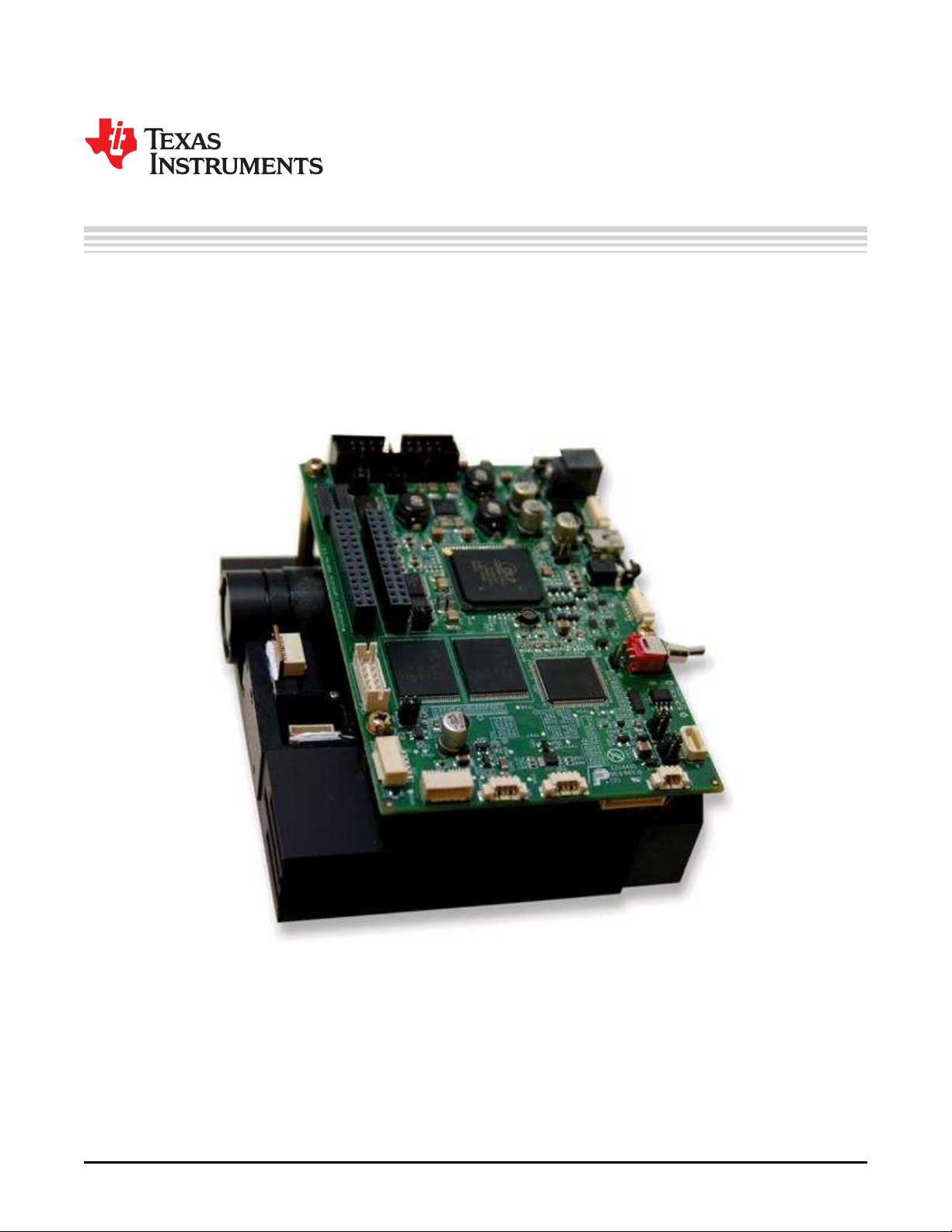
Figure 1. DLP LightCrafter 4500 Evaluation Module (EVM)
6
Read This First DLPU011E–July 2013–Revised September 2015
Copyright © 2013–2015, Texas Instruments Incorporated
Submit Documentation Feedback
Page 7

www.ti.com
Related Documentation From Texas Instruments
DLPC350 data sheet: DLP Digital Controller for the DLP4500 DMD, DLPS029
DLP4500 data sheet: DLP 0.45 WXGA DMD, DLPS028
DLPC350 and DLP4500 chipset manual: DLP 0.45 WXGA Chipset Data Manual, DLPU009
User's guide: DLPC350 Programmer’s Guide, DLPU010
Application note: Using DLP®LightCrafter 4500™ Triggers to Synchronize Camera, DLPA036
If You Need Assistance
Refer to the DLP and MEMS TI E2E Community support forums: DLP LightCrafter 4500 Development
Platform Forum
Related Documentation From Texas Instruments
LightCrafter 4500 is a trademark of Texas Instruments.
DLP, Linux are registered trademarks of Texas Instruments.
Bluetooth is a registered trademark of Bluetooth SIG, Inc..
Ubuntu is a registered trademark of Canonical Ltd..
SVTronics is a registered trademark of SVTRONICS, INC..
Sullins Connector Solutions is a registered trademark of Sullins Connector Solutions, Inc..
DLPU011E–July 2013–Revised September 2015 Read This First
Submit Documentation Feedback
Copyright © 2013–2015, Texas Instruments Incorporated
7
Page 8

If You Need Assistance
www.ti.com
8
Read This First DLPU011E–July 2013–Revised September 2015
Copyright © 2013–2015, Texas Instruments Incorporated
Submit Documentation Feedback
Page 9

1.1 Welcome
The DLP LightCrafter 4500 evaluation module (EVM) allows evaluation of the DLP 4500 platform from TI.
This technology brings together a set of components providing an efficient and compelling system solution
for:
• 3D scanning structured light applications:
– 3D modeling and design
– Fingerprint identification and face recognition
– Machine vision and robotic factory automation
– Industrial inspection
• Medical and life sciences:
– Vascular imaging
– Hyperspectral imaging
– Dental impression scanners
– Intraoral dental scanners
– Orthopedics, prosthesis, CT, MRI, and X-ray marking
– Retail cosmetics
• Small display projectors:
– Embedded display
– Interactive display
– Information overlay
• Spectroscopy and chemical sensing
– Material identification
– Oil & Gas analysis
– Water & air quality
– Food & drug inspection
– TI NIRscan EVM uses the DLP4500NIR DMD (similar to the DLP4500 in the LightCrafter4500 EVM
and optimized for near-infrared light) in structured light mode to provide a high performance and
cost-competitive spectroscopy solution
Chapter 1
DLPU011E–July 2013–Revised September 2015
DLP LightCrafter 4500 Module Overview
1.2 What is in the LightCrafter 4500 EVM?
The DLP LightCrafter 4500 module consists of two subsystems:
• Light engine – includes the optics; red, green, and blue LEDs; and the 912 × 1140 diamond pixel 0.45inch WXGA DMD, heat sinks, and fan. The light engine produces approximately 150 lumens at 15-W
LED power consumption.
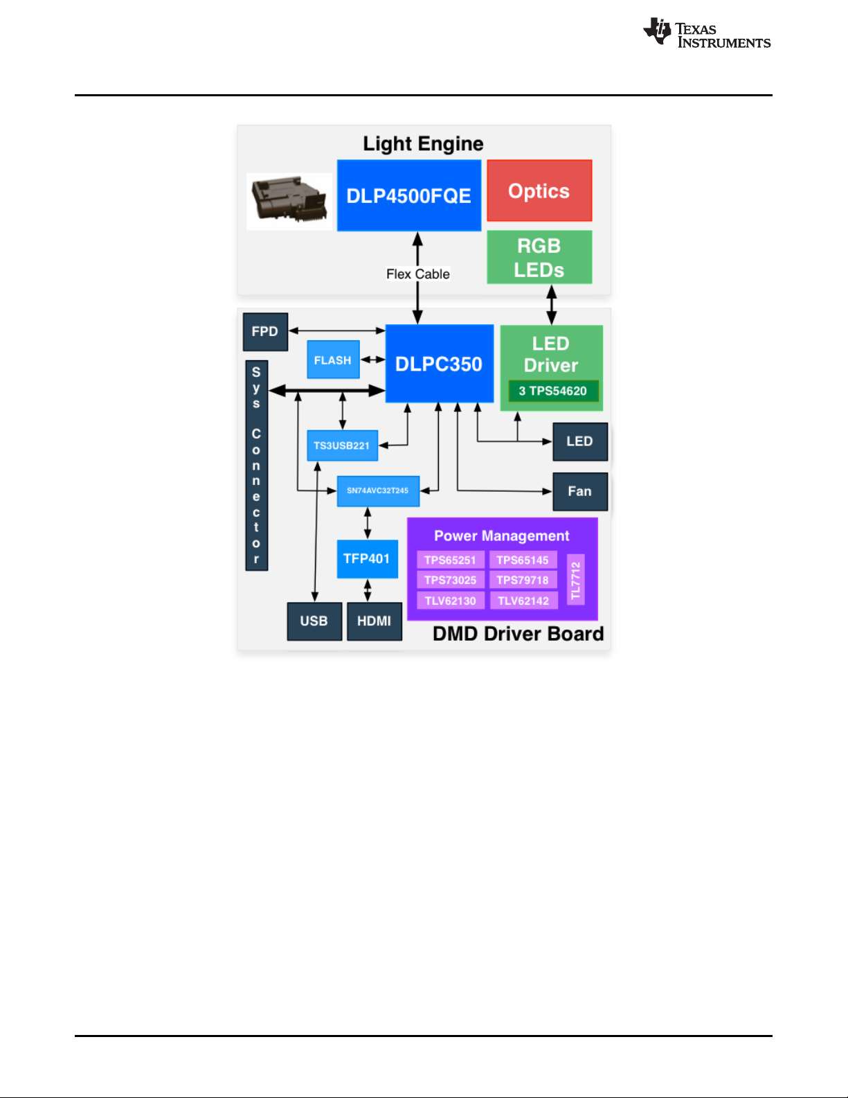
• Driver board – includes the LED driver circuits, DLPC350 DMD controller, power-management circuits,
DVI-to-RGB conversion with the TFP401, and a 32-MB flash storage
Figure 1-1 shows the major hardware components.
DLPU011E–July 2013–Revised September 2015 DLP LightCrafter 4500 Module Overview
Submit Documentation Feedback
Copyright © 2013–2015, Texas Instruments Incorporated
9
Page 10
What is in the LightCrafter 4500 EVM?
www.ti.com
1.2.1 Light Engine
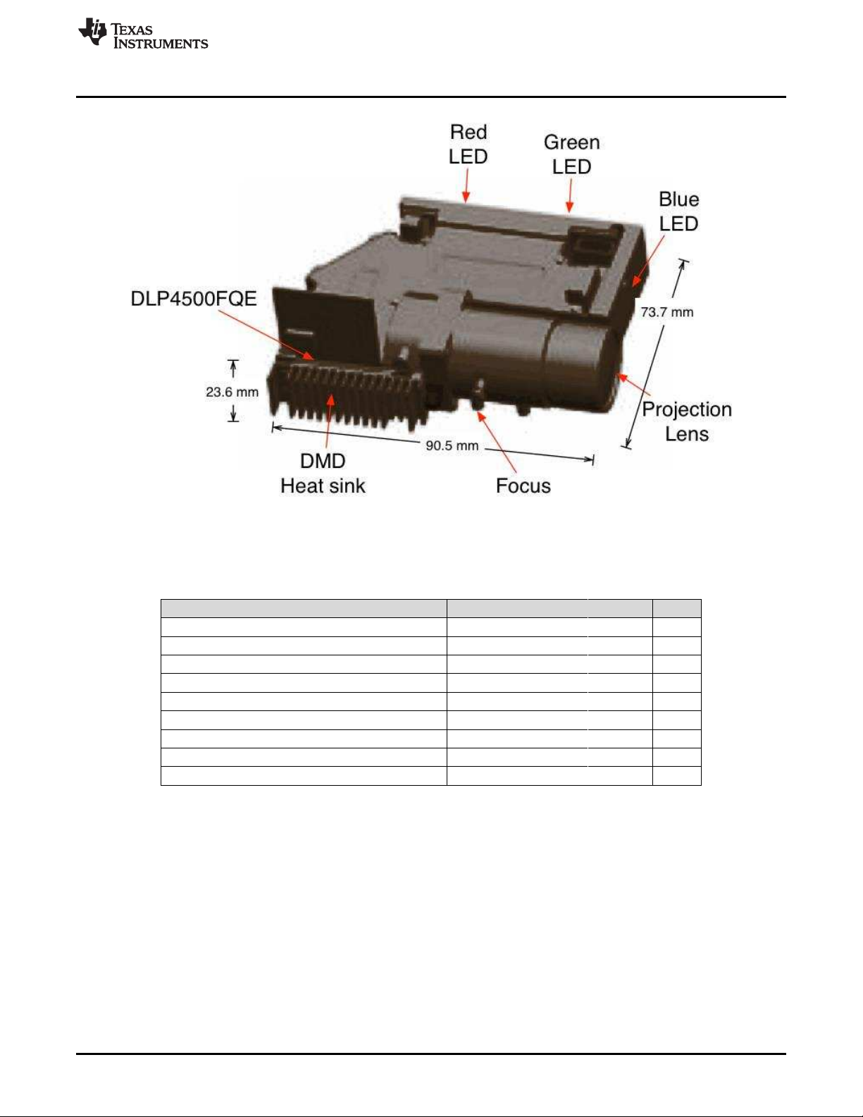
iView Limited developed the IPD 1231 light engine for the DLP LightCrafter 4500. As shown in Figure 1-2,
the light engine includes:
• DLP4500FQE DMD
• DMD heat sink
• Red, green, and blue LEDs
• Focus control
• Projection lens
The iView Light Engine is mounted on top of a large thermal plate to cool the module. The DLP4500 DMD
is mounted vertically between the DMD heat sink and the light engine. On the opposite side to the DMD,
the red and green LEDs are mounted between a thermal plate and the light engine. The blue LED is
mounted between a thermal plate and the light engine, next to the projection lens. An LED heat sink is
mounted behind the red and green LED thermal plate and thermally connected to the blue LED thermal
plate. A fan forces air across the LED heat sink to cool the LEDs.
The light engine, not including the LED heat sinks, has a length of 90.5 mm, width of 73.7 mm, and height
of 23.6 mm.
10
DLP LightCrafter 4500 Module Overview DLPU011E–July 2013–Revised September 2015
Figure 1-1. DLP LightCrafter 4500 Block Diagram
Copyright © 2013–2015, Texas Instruments Incorporated
Submit Documentation Feedback
Page 11
www.ti.com
What is in the LightCrafter 4500 EVM?
Figure 1-2. iView Light Engine
Table 1-1 lists the specifications of the light engine:
Table 1-1. DLP LightCrafter Light Engine Specifications
Parameter MIN TYP MAX UNIT
Brightness 150 lm
LED power consumption 15 W
Full-on full-off contrast 1000:1
Uniformity 80 90 %
F-number 2.1
Throw ratio 1.4
Offset 100 %
Focus range 0.5 1 2 m
Image diagonal size 16.7 32.8 65 inch
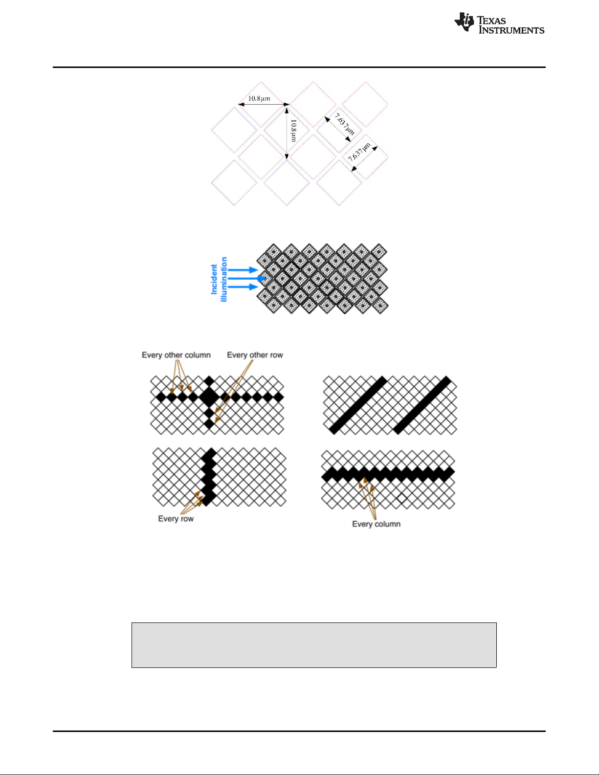
The light engine includes the DLP4500 0.45-inch DMD with 1039680 mirrors, each 7.6 µm, arranged in
912 columns by 1140 rows with the diamond pixel array geometry and configuration (see Figure 1-3 and
Figure 1-4). Due to the diamond pixel configuration, the array produces smooth diagonal lines, with jagged
vertical and horizontal lines, as shown in Figure 1-5. Two options exist to produce the vertical and
horizontal lines: use every row or column, or use every other row or column. When every row or column is
used, a more thick line is projected. When every other row or column is used, a more faint line is
projected.
DLPU011E–July 2013–Revised September 2015 DLP LightCrafter 4500 Module Overview
Submit Documentation Feedback
Copyright © 2013–2015, Texas Instruments Incorporated
11
Page 12
What is in the LightCrafter 4500 EVM?
Figure 1-3. 0.45-Inch DMD Diamond Pixel Geometry
Figure 1-4. 0.45-Inch DMD Diamond Pixel Array Configuration
www.ti.com
Figure 1-5. Diamond Pixel for Vertical, Horizontal, and Diagonal Lines
1.2.1.1 Light Engine Thermal Limits
The DLP LightCrafter 4500 is an actively cooled system with a thermal limit requiring that of all three
simultaneous LED currents is less than 4.3 A.
Do not overheat the system by driving all LEDs at maximum power.
12
DLP LightCrafter 4500 Module Overview DLPU011E–July 2013–Revised September 2015
Copyright © 2013–2015, Texas Instruments Incorporated
CAUTION
Submit Documentation Feedback
Page 13
www.ti.com
1.2.2 Driver Board
The DLP LightCrafter 4500 driver board contains the electronics to drive the DLP4500 DMD, LEDs of the
light engine, and the LED cooling fan. The driver board offers several interface options for USB, I2C,
trigger inputs and outputs, video input through mini-HDMI and FPD-link connector, and a system board
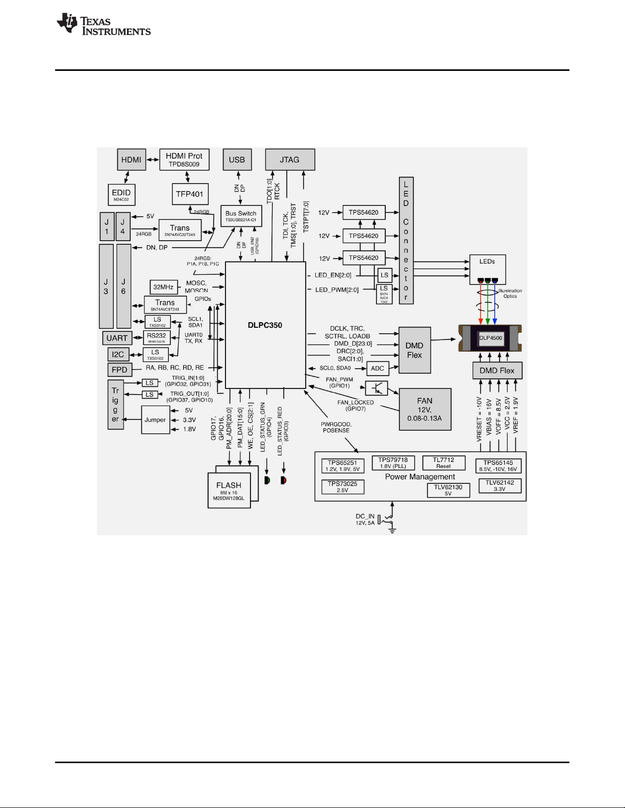
interface. Figure 1-6 shows the driver board block diagram of the DLP LightCrafter 4500.
What is in the LightCrafter 4500 EVM?
Figure 1-6. DLP LightCrafter 4500 Driver Board Block Diagram
The DLP LightCrafter 4500 driver board major components are:
• DLP4500: 0.45 inch-WXGA DMD
• DLPC350: DLP4500 controller
• 32-MB parallel flash contains DLPC350 firmware and 24-bit compressed images
• TPS54620: Synchronous step-down converter serving as an LED driver capable of driving up to 5 A
per LED
• Power management:
– TPS65251: Triple output buck switcher for DLPC350 1.2-V, 1.9-V supplies and 5-V board supply.
– TPS65145: Triple output boost converter for DLP4500 8.5-, –10-, and 16-V supplies
– TPS73025: Step-down converter for DLP4500 2.5-V supply
– TLV62130: Step-down converter for 3.3-V supply
– TLV62130: Step-down converter for 5-V system board supply
– TPS79718: LDO for DLPC350 1.8-V analog supply
DLPU011E–July 2013–Revised September 2015 DLP LightCrafter 4500 Module Overview
Submit Documentation Feedback
Copyright © 2013–2015, Texas Instruments Incorporated
13
Page 14

What is in the LightCrafter 4500 EVM?
– TL7712: Programmable time delay for power-supply sequencing
• TFP401: Digital Receiver for DVI to 24-bit parallel RGB interface
• TS3USB2221A: ESD-protected high-speed USB multiplexer
• SN74AVC32T245: 32-bit dual supply bus transceiver for system board interface
1.2.3 Embedded Processor Interface
The DLP LightCrafter 4500 driver board allows the connection of a PandaBoard ES. See, Chapter 6.
1.3 Other Items Needed for Operation
The DLP LightCrafter 4500 module is a flexible, ready-to-use EVM. However, the DLP LightCrafter 4500
EVM does not ship with cables, power supply, or additional hardware components. To use the EVM, the
user needs the following:
• Power supply:
– Nominal voltage: 12-V DC
– Typical current: 6 A
– Maximum current: 7 A
– DC connector size:
• Inner diameter: 2.5 mm
• Outer diameter: 5.5 mm
• Shaft: 9.5-mm female, center positive
– Efficiency level: V
– A recommended power supply is Digi-Key part number 62-1186-ND , or equivalent.
• USB cable: A to mini-B USB cable
• Optional: PandaBoard 4500
www.ti.com
14
DLP LightCrafter 4500 Module Overview DLPU011E–July 2013–Revised September 2015
Copyright © 2013–2015, Texas Instruments Incorporated
Submit Documentation Feedback
Page 15

www.ti.com
1.4 DLP LightCrafter 4500 Connections
Figure 1-7 and Figure 1-8 depict the switches and connectors with their respective locations. The following
list corresponds to the callouts on these figures. The figure does not include cables, or a power supply.
1. Reset button
2. Power connector: Use a power supply with a 12-V DC output with current of 6 to 7-A rating and a plug
of 2.5-mm inner diameter × 5.5-mm outer diameter and 9.5-mm female center positive shaft. The
current output of the power supply determines how much current the LED driver can supply
3. External trigger output connector: Supports two trigger output signals, each with configurable voltage of
3.3 V and 1.8 V through jumpers, J13 and J15, respectively.
4. Mini-USB connector: use an A to mini-B USB cable to connect to a PC.
5. UART/RS232 mini-plug connector output: DLPC350 3.3-V UART output for error messages. Mini-plug
tip is DLPC350 transmit (TX) and ring is DLPC350 receive (RX) signals. UART has the following serial
configuration:
• Bits per second: 115200
• Data bits: 8
• Parity: None
• Stop bits: 1
• Flow control: None
6. External trigger Input connector: Supports two trigger input signals, each with configurable voltage of
5 V, 3.3 V and 1.8 V through jumpers, J10 and J12
7. Stand-by switch: Places the DLP LightCrafter 4500 in standby mode, powering down the LED driver
and the DLPC350
8. Flat panel display-link connector
9. Fan connector
10. Red LED supply connector (bottom of the board)
11. DLPC350 I2C1 bus
12. DLPC350 I2C0 bus
13. Green LED supply connector
14. Blue LED supply connector
15. External LED driver connector: Install a jumper in J30 to disable the DLP LightCrafter 4500 LED
drivers and set jumper J28 for 3.3-V or 1.8-V supply. Then use this connector to control an external
LED driver board to power the LEDs of the DLP LightCrafter 4500 light engine or external light engine.
16. System board connector: This interface routes USB, I2C, GPIO, and triggers from DLPC350 to a
system board to control the DLP LightCrafter 4500.
17. Focus control (bottom of the board): Adjust focus from 0.5 m to infinity
18. JTAG connector for DLPC350
19. JTAG Boundary Scan for DLPC350 (bottom of the board)
20. DVI input through mini-HDMI connector (bottom of the board). This input supports resolutions of 1280
× 800, 1024 × 768, 1024 × 640, 912 × 1140, 800 × 600, 800 × 500, and 640 × 480 at up to 120 Hz. In
Video Mode, the DLPC350 scales the input resolution to the native resolution of the DLP4500 DMD. In
Pattern Sequence mode, this input supports 912 × 1140 resolution.
DLP LightCrafter 4500 Connections
DLPU011E–July 2013–Revised September 2015 DLP LightCrafter 4500 Module Overview
Submit Documentation Feedback
Copyright © 2013–2015, Texas Instruments Incorporated
15
Page 16
DLP LightCrafter 4500 Connections
www.ti.com
Figure 1-7. DLP LightCrafter 4500 Connectors (Top View)
16
Figure 1-8. DLP LightCrafter 4500 Connectors (Back-Side View)
DLP LightCrafter 4500 Module Overview DLPU011E–July 2013–Revised September 2015
Copyright © 2013–2015, Texas Instruments Incorporated
Submit Documentation Feedback
Page 17
www.ti.com
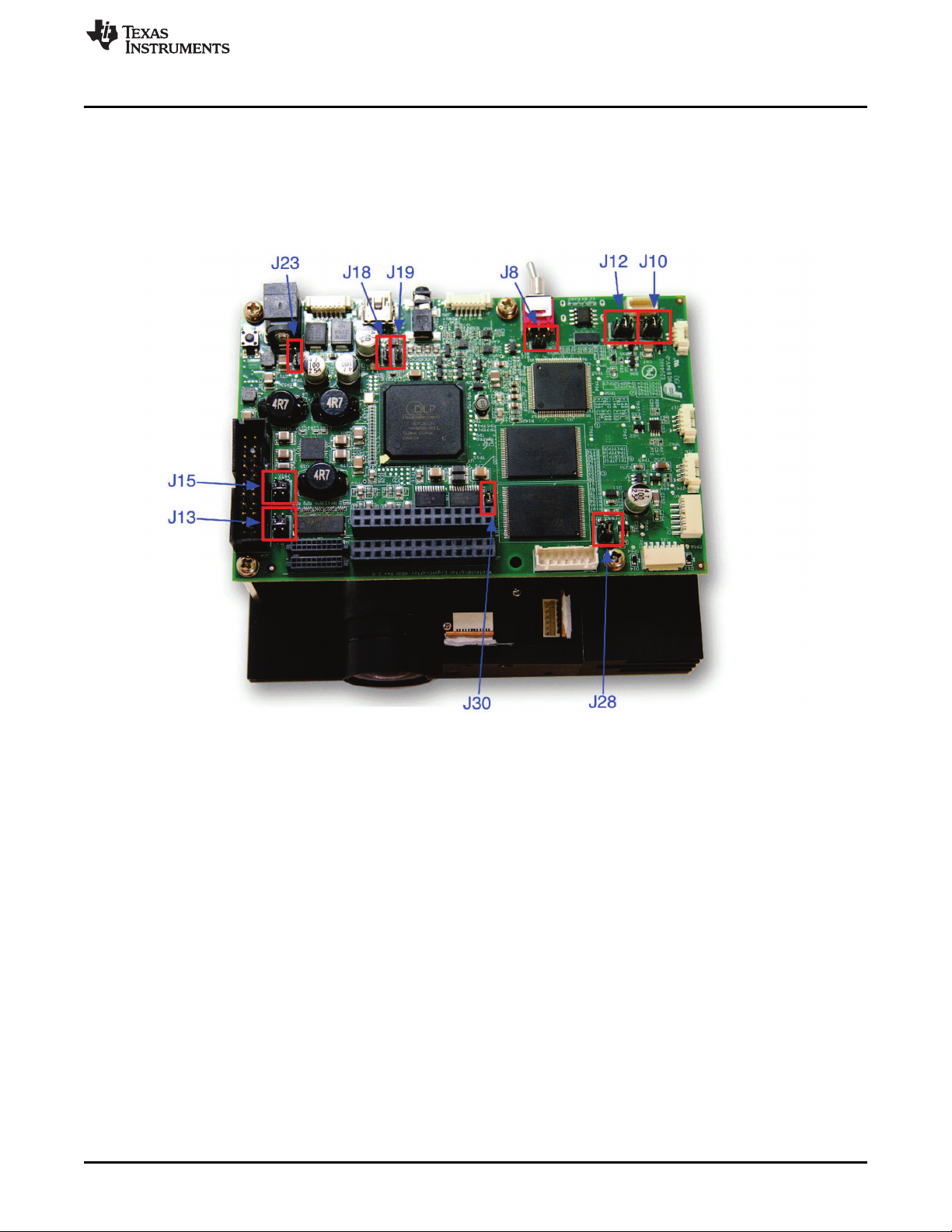
1.5 DLP LightCrafter 4500 Jumpers
The DLP LightCrafter 4500 has jumper options to disable the onboard LED driver, control voltages of the
LED signals to an external board, and control the trigger input and output voltages. This section lists all
the jumpers on the DLP LightCrafter 4500 driver board. Figure 1-9 depicts the locations of these jumpers.
These jumpers require a 2-mm jumper, like Sullins Connector Solutions®SPN02SYBN-RC, Digi-Key part
number S3404-ND.
DLP LightCrafter 4500 Jumpers
Figure 1-9. DLP LightCrafter 4500 Jumper Locations
• J8: EDID write protect disable jumper. Place this jumper to reprogram the EDID EEPROM (U2) using
I2C commands through the mini-HDMI connector. Remove the jumper when programming of the EDID
is complete. The EDID is programmed at the factory with resolutions of 1280 x 800 and 912 x 1140.
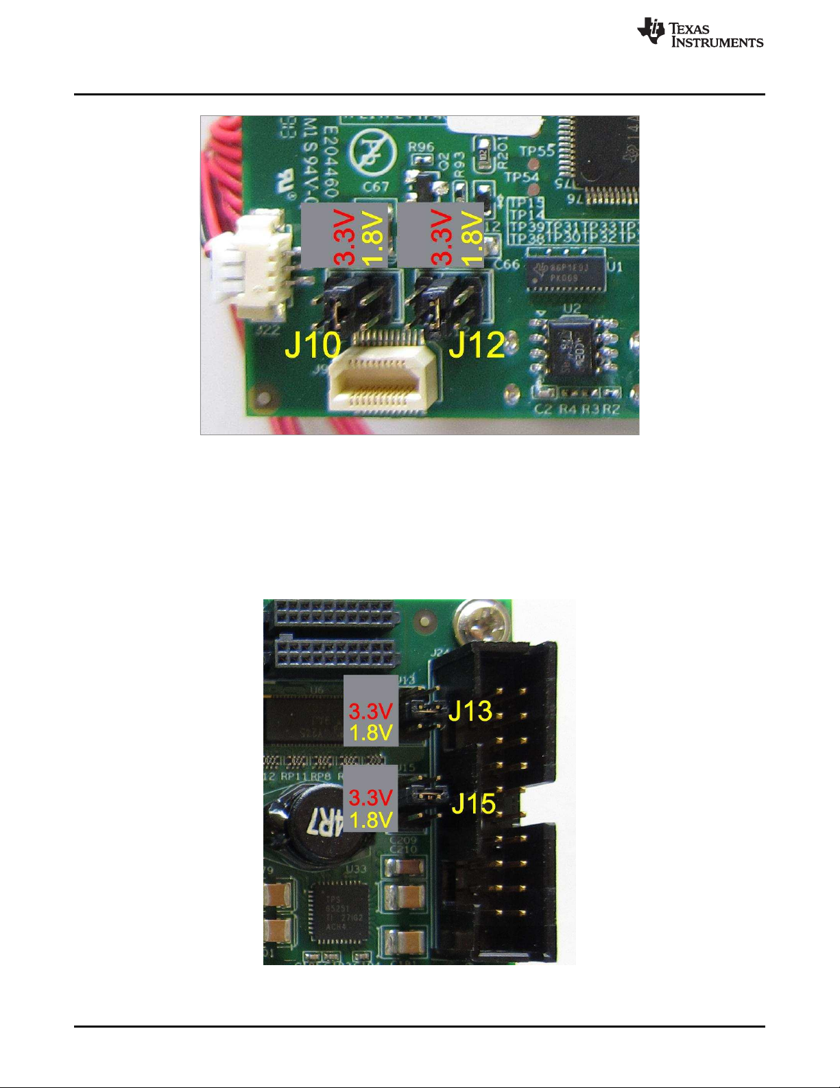
• J10: DLPC350 TRIG1_IN voltage selection. See to Figure 1-10.
– Jump across pins 3 to 4 for 3.3 V
– Jump across pins 5 to 6 for 1.8 V
• J12: DLPC350 TRIG2_IN voltage selection. See to Figure 1-10.
– Jump across pins 3 to 4 for 3.3 V
– Jump across pins 5 to 6 for 1.8 V
DLPU011E–July 2013–Revised September 2015 DLP LightCrafter 4500 Module Overview
Submit Documentation Feedback
Copyright © 2013–2015, Texas Instruments Incorporated
17
Page 18
DLP LightCrafter 4500 Jumpers
Figure 1-10. DLP LightCrafter 4500 J10 and J12 Voltage Jumpers
• J13: DLPC350 TRIG1_OUT voltage selection. See to Figure 1-11.
– Jump across pins 3 to 4 for 3.3 V
– Jump across pins 5 to 6 for 1.8 V
• J15: DLPC350 TRIG2_OUT voltage selection. See to Figure 1-11.
– Jump across pins 3 to 4 for 3.3 V
– Jump across pins 5 to 6 for 1.8 V
www.ti.com
18
Figure 1-11. DLP LightCrafter 4500 J13 and J15 Voltage Jumpers
• J18: DLPC350 HOLD_IN_BOOT. Jump across this header to hold the DLPC350 in bootloader mode.
DLP LightCrafter 4500 Module Overview DLPU011E–July 2013–Revised September 2015
Copyright © 2013–2015, Texas Instruments Incorporated
Submit Documentation Feedback
Page 19

www.ti.com
This action is needed only if the DLP LightCrafter 4500 firmware becomes corrupted and must be
reprogrammed through the JTAG boundary scan or USB. The graphical user interface (GUI) firmware
upgrade process places the DLPC350 in bootloader mode through software commands and does not
need the jumper.
• J19: Device address select
– Jump across header to set I2C address to 0x3A and USB device serial number to LCR2.
– Do not populate jumper to set I2C address to 0x34 and USB device serial number to LCR2.
• J23: Hold in reset. Jump across header to drive and hold reset line low. Jumping across this header is
equivalent to pressing and holding the reset switch.
• J28: DLPC350 LED signals voltage selection. This jumper must be populated when bypassing the
onboard LED driver and using an external LED driver.
– Jump across pins 1 to 2 to set the DLPC350 LED enables and PWM signals to 3.3 V.
– Jump across pins 3 to 4 to set the DLPC350 LED enables and PWM signals to 1.8 V.
• J30: DLPC350 LED driver disable. This jumper must be populated when bypassing the onboard LED
driver and using an external LED driver.
– Jump across header to disable the onboard LED driver and turn off all LEDs, regardless of the DLP
LightCrafter 4500 video mode.
– Do not populate this header for normal operation using the onboard LED driver.
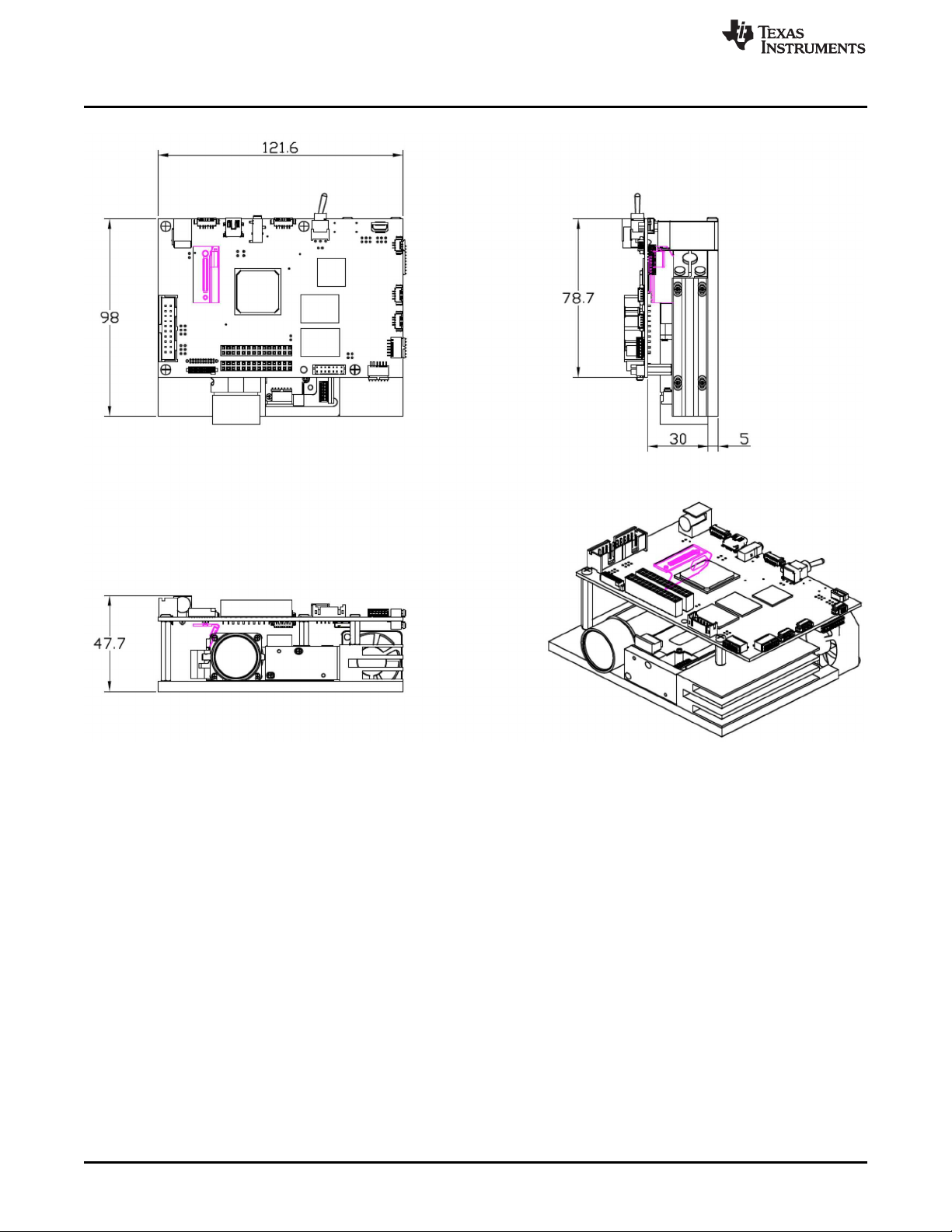
1.6 Dimensions
The DLP LightCrafter 4500 optical engine is mounted on top of a thermal plate to provide passive cooling
to the module. A heat sink and fan provide active cooling to the LEDs. The DLP4500, 0.45-in. DMD, is
vertically mounted at the end of the optical engine and attached with a flex cable to the driver board that
lies on top of the light engine. The dimensions of the DLP LightCrafter 4500 are of 98 mm long, 121.6 mm
wide, and 47.7 mm tall. Figure 1-12 shows DLP LightCrafter 4500 dimensions.
Dimensions
DLPU011E–July 2013–Revised September 2015 DLP LightCrafter 4500 Module Overview
Submit Documentation Feedback
Copyright © 2013–2015, Texas Instruments Incorporated
19
Page 20
Dimensions
www.ti.com
20
Figure 1-12. DLP LightCrafter 4500 Dimensions
DLP LightCrafter 4500 Module Overview DLPU011E–July 2013–Revised September 2015
Copyright © 2013–2015, Texas Instruments Incorporated
Submit Documentation Feedback
Page 21

www.ti.com
Dimensions
DLPU011E–July 2013–Revised September 2015 DLP LightCrafter 4500 Module Overview
Submit Documentation Feedback
Copyright © 2013–2015, Texas Instruments Incorporated
21
Page 22

This chapter details the steps to power up the DLP LightCrafter 4500 and connect to a PC.
2.1 Power-up the DLP LightCrafter 4500
The DLP LightCrafter 4500 is ready to use, out of the box. Steps 1 through 5 show how to power, display
an image, and connect the device to a PC.
1. Connect a 12-V DC power supply to the power supply connector (connector 2 in Figure 1-8).
2. An LED on the bottom of the LightCrafter 4500 board, next to the flex cable lights up green. The fan
starts, stops, and then restarts while the DLPC350 is booting. After 5 to 10 seconds, the DLPC350
bootloads and displays a screen with the DLP and LightCrafter 4500 logo. The D4 LED on top of the
LightCrafter 4500 board flashes on and off green. If the board shuts down after briefly turning on the
display, the power supply current rating might be too low.
3. To display video, connect a DVI source to the mini-HDMI connector (connector 20 in Figure 1-8).
4. Control the DLP LightCrafter 4500 with the free GUI software (available to download from
http://www.ti.com/dlplightcrafter4500).
5. After installing the software on the computer, connect the PC to the DLP LightCrafter 4500 using a
USB to mini-USB cable (connector 4 in Figure 1-8). The first time the cable is connected on a PC, the
DLP LightCrafter 4500 emulates a USB composite device with human-interface device (HID) class. No
drivers are required because these drivers are natively handled by all operating systems.
Chapter 2
DLPU011E–July 2013–Revised September 2015
Quick Start
22
Quick Start DLPU011E–July 2013–Revised September 2015
Copyright © 2013–2015, Texas Instruments Incorporated
Submit Documentation Feedback
Page 23

www.ti.com
Power-up the DLP LightCrafter 4500
DLPU011E–July 2013–Revised September 2015 Quick Start
Submit Documentation Feedback
Copyright © 2013–2015, Texas Instruments Incorporated
23
Page 24

This chapter introduces the PC software provided with the DLP LightCrafter 4500.
3.1 DLP LightCrafter 4500 Software
The DLP LightCrafter 4500 includes a QT-based GUI application to control the module through the USB
interface. QT is a Nokia cross-platform application and user-interface framework with open source and
commercial licenses. To install the QT GUI, just expand the LightCrafter4500_GUI.zip file into a directory
and double-click on the executable file.
The DLP LightCrafter 4500 supports three main modes of operation:
• Video mode displays images from:
– DVI input through the mini-HDMI connector
– 24-bit RGB bitmaps stored in flash memory
– 24, 20, 16, 10, and 8-bit RGB input through the system board connectors (J1, J3, J4, and J6)
– Internal test patterns
– 30-bit RGB through flat panel display (FPD) link
• Pattern Sequence mode displays images from:
– 1-, 2-, 3-, 4-, 5-, 6-,7-, and 8-bit bitmap images stored in flash memory
– 1-, 2-, 3-, 4-, 5-, 6-, 7-, and 8-bit bitmap images streamed through the DLPC350 24-bit RGB
interface (mini-HDMI, FPD-link, or system board connectors)
– The chosen pattern exposure and pattern period times apply to all patterns in the pattern sequence
• Pattern Sequence [Variable Exposure] mode displays images from the same sources as Pattern
Sequence mode:
– 1-, 2-, 3-, 4-, 5-, 6-,7-, and 8-bit bitmap images stored in flash memory
– 1-, 2-, 3-, 4-, 5-, 6-, 7-, and 8-bit bitmap images streamed through the DLPC350 24-bit RGB
interface (mini-HDMI, FPD-link, or system board connectors)
– This mode allows for the pattern exposure time and pattern period to be set per pattern in the
pattern sequence
Chapter 3
DLPU011E–July 2013–Revised September 2015
Operating the DLP LightCrafter 4500
3.2 PC Software
Upon execution of the LightCrafter4500.exe file, the window shown in Figure 3-1 displays. The GUI
window contains the following two sections:
• The top portion of the GUI window displays the System Control and controls the Operating Mode,
Image Orientation, LED Driver Control settings, and LED Selection. There are also controls for saving
and applying solutions.
• The bottom portion of the GUI window offers a set of tabs to further control the selected Operating
Mode.
In any of the GUI sections, clicking a Get button reads the current settings of that particular subsection.
Clicking the Set button programs the settings in the respective subsection. Some commands may require
additional steps before the GUI display is updated.
24
Operating the DLP LightCrafter 4500 DLPU011E–July 2013–Revised September 2015
Copyright © 2013–2015, Texas Instruments Incorporated
Submit Documentation Feedback
Page 25

www.ti.com
PC Software
Figure 3-1. DLP LightCrafter 4500 GUI – Video Mode
The DLP LightCrafter 4500 GUI communicates with the DLPC350 using USB 1.1. The DLPC350 emulates
as a USB device with HID support. The PC polls all the HID peripherals and once the PC detects the
DLPC350, the Connected button changes to green. If the USB cable is disconnected, the color of the
Connected button changes to red and the Connected text is grayed-out. Once the System Status shows
Connected, the firmware version, firmware tag, hardware, and System Status indicators are displayed.
There is no need to press the Connected button, because the HID peripheral is detected by the operating
system after USB enumeration.
3.2.1 System Status
At the top-left portion of the GUI window, the hardware and System Status indicators report the following:
• Init Done: When highlighted green, it indicates the successful completion of the DLPC350 initialization.
When highlighted grey, it indicates the DLPC350 had an error during initialization.
• Sequencer Running: When highlighted green, the DLPC350 sequencer is running as usual. When
highlighted gray, the DLPC350 sequencer is stopped.
• DRC Error: DMD Reset Controller Error indicator. When highlighted grey, the DMD Reset Controller
has not detected an error. When highlighted red, the DMD Reset Controller has found multiple
overlapping bias or reset operations accessing the same DMD block of micromirrors.
DLPU011E–July 2013–Revised September 2015 Operating the DLP LightCrafter 4500
Submit Documentation Feedback
Copyright © 2013–2015, Texas Instruments Incorporated
25
Page 26

PC Software
• Forced Swap: When highlighted red, the DLPC350 sequencer detected a forced buffer swap error
indicating that image data has been displayed from the wrong internal display buffer. When highlighted
gray, no buffer swap error has occurred. This error can occur if the DLP LightCrafter 4500 is set to
Video Mode and the vertical backporch timing is too small. The error can also occur if the DLP
LightCrafter 4500 is set to Pattern Sequence mode with patterns input from the video port and pattern
sequence timings do not match the video port VSYNC.
• Sequencer Error: When highlighted red, the DLPC350 sequencer has detected an error. When
highlighted gray, the DLPC350 sequencer detected that no error occurred.
• DMD Parked: When highlighted yellow, the DMD micromirrors are parked in the position normal to the
DMD plane. When highlighted gray, the DMD micromirrors are not parked.
• Buffer Freeze: When highlighted yellow, the frame buffer is frozen. When highlighted gray, the frame
buffer is not frozen. This is cleared on the next buffer swap.
• Sequencer Abort: When highlighted red, the DLPC350 sequencer has detected an error condition that
caused an abort. When highlighted gray, the DLPC350 sequencer detected that no error occurred.
These indicators are updated every 2 seconds, or when a command is issued to the DLPC350.
• Auto Update Status. When checked, all indicators will continue to update every two seconds. When
unchecked, the indicators will stop updating and turn gray. While running in Pattern Sequence Mode,
keeping the option unchecked prevents the GUI from interrupting the DLPC350 controller which will be
processing critical functions related to pattern display.
3.2.2 Operating Mode
To the right of the System Status, the Operating Mode sets how the DLP LightCrafter 4500 operates:
• Pattern Sequence mode: The DLPC350 takes 1-, 2-, 3-, 4-, 5-, 6-, 7-, and 8-bit data from one of the
following interfaces:
– 24-bit RGB interface
– FPD-link interface
– Flash memory
www.ti.com
The DLPC350 does not apply any video processing functions and provides a pixel accurate mode
where every pixel maps to the native DMD resolution of 912 × 1140.
• Pattern Sequence [Variable Exposure] mode: The DLPC350 takes 1-, 2-, 3-, 4-, 5-, 6-, 7-, and 8-bit
data from one of the following interfaces:
– 24-bit RGB interface
– FPD-link interface
– Flash memory
This mode differs from Pattern Sequence mode in that the pattern exposure time and pattern period
can be varied per pattern in the pattern sequence.
The DLPC350 does not apply any video processing functions and provides a pixel accurate mode
where every pixel maps to the native DMD resolution of 912 × 1140.
• Video Mode: The DLPC350 takes 24, 20, 16, 10, and 8-bit data from one of the following interfaces:
– 24-bit RGB interface
– FPD-link interface
– Internal test pattern generator
– Flash memory
The DLPC350 then applies video processing functions, such as scaling, gamma correction, and color
coordinate adjustments, and sends the processed image to the DMD.
• Power Standby: Places the DLPC350 in low-power state and powers down the DMD interface.
26
Operating the DLP LightCrafter 4500 DLPU011E–July 2013–Revised September 2015
Copyright © 2013–2015, Texas Instruments Incorporated
Submit Documentation Feedback
Page 27

www.ti.com
3.2.3 Image Orientation
Beneath Operating Mode, the Image Orientation controls the long and short axis flips to support front,
rear, table, and ceiling mounted projection. The Image Orientation occurs on the next image or frame load
in Video mode, and on the next download to the DLP LightCrafter 4500 in Pattern Sequence mode.
• East/West Flip: If checked, the image is flipped along the east and west axis of the projected image.
Usual table front projection has this setting unchecked. Otherwise, the image is flipped horizontally.
• North/South Flip: If checked, the image is flipped along the north and south axis of the projected
image. Usual table front projection has this setting unchecked. Otherwise, the image is flipped
vertically.
PC Software
DLPU011E–July 2013–Revised September 2015 Operating the DLP LightCrafter 4500
Submit Documentation Feedback
Copyright © 2013–2015, Texas Instruments Incorporated
27
Page 28

PC Software
3.2.4 LED Current Settings
On the top-right of the GUI window, the LED Current settings control the individual currents of the red,
green, and blue LEDs. A setting of 255 corresponds to the maximum LED current. A setting of 0
corresponds to minimum LED current. The LED current is computed as follows:
Red LED Current (A) = 0.0175 × (LED Current Value) + 0.4495 (1)
Green LED Current (A) = 0.0181 × (LED Current Value) + 0.3587 (2)
Blue LED Current (A) = 0.0160 × (LED Current Value) + 0.1529 (3)
Typical performance of the red, green, and blue LEDs are shown in Figure 2, Figure 3, and Figure 4,
respectively. Manufacturing processes can lead to variations in LED brightness and current consumption.
Actual LED performance might vary from those shown in the following figures.
www.ti.com
Figure 2. Typical Red LED Current and Illuminance Based Figure 3. Typical Green LED Current and Illuminance
on PWM Values Based on PWM Values
Figure 4. Typical Blue LED Current and Illuminance Based on PWM Values
CAUTION
The DLP LightCrafter 4500 is an actively cooled system that has a thermal limit
resulting in total simultaneous red, green, and blue LED currents less than
4.3 A for continuous LED operation. Do not overheat the system by turning all
LEDs at maximum power during prolonged and simultaneous LED use.
Exceeding more than 4.3 A for continuous or simultaneous LED operation can
damage the LightCrafter 4500 LEDs.
28
Operating the DLP LightCrafter 4500 DLPU011E–July 2013–Revised September 2015
Copyright © 2013–2015, Texas Instruments Incorporated
Submit Documentation Feedback
Page 29

www.ti.com
Typical variations in LED manufacturing can lead to changes in the brightness and current consumption.
Thus for typical white balance point, TI recommends the following percentages of colors:
• Red or green is approximately 87.5%
• Blue or green is approximately 97.6%
At the default LED current values of:
• Red = 104
• Green = 135
• Blue = 130
The LED Selection box determines the control of the LED enables signals. Two options are allowed:
• Automatic: LED enables are controlled by the DLPC350 sequencer. In Video Mode, the LED enables
are set in color sequential order. In Pattern Sequence mode, the LED enables are controlled by the
downloaded Pattern Sequence settings.
• Manual: LED enables are controlled by the check boxes. Checking a color, continuously enables the
LED of that color at the given LED current setting.
3.2.5 Video Mode
When the DLP LightCrafter 4500 is configured in Video Mode, the Input Source Select section in Figure 3-
1 in the top-left part of the Video Mode tab selects the input source to be displayed by the DLPC350. The
DLPC350 treats these as video inputs and applies image processing functions, like scaling, gamma
correction, color coordinate adjustments, and so forth. The following lists the allowable input sources:
• Parallel RGB interface: Supports 24-, 20-, 16-, 10-, and 8-bit data inputs. This interface is connected to
the TFP401 for DVI input from the mini-HDMI connector or to the system board connectors. The Pixel
Data Format section is below the Source Select interface selects the allowable pixel data formats for
the Parallel RGB interface:
– RGB 4:4:4
– YCrCb 4:4:4
– YCrCb 4:2:2
• Internal Test Pattern: 24-bit internal pattern generator with RGB 4:4:4 pixel data format. The internal
test patterns offer color control of the foreground and background color of the pattern through the
Internal Test Pattern Color section. The available internal test patterns and their respective foreground
and background color control are:
– Solid field: Foreground color control only
– Horizontal ramp: Foreground color control only
– Vertical ramp: Foreground color control only
– Horizontal lines: Foreground and Background color control
– Diagonal lines: Foreground and Background color control
– Vertical lines: Foreground and Background color control
– Grid: Foreground and Background color control
– Checkerboard: Foreground and Background color control
– Red, green, and blue ramps: Foreground color control only
– Color bar: Foreground color control only
– Step bar: Foreground color control only
• Flash images: single-frame, 24-bit Still images stored in external flash memory. The flash memory
supports up to 32MB of storage with up to 64 images. The images stored in flash memory support
RGB 4:4:4 and YCrCb 4:2:2 pixel data formats.
• FPD-link: Flat Panel Display Link connector. The FPD-link interface supports 30-, 24-, 20-, 16-, 10-,
and 8-bit data inputs with RGB 4:4:4 pixel data format. The FPD Mode and Field Select configures the
mapping of the pixel mode, polarity, and CONT1 and CONT2 field signals.
PC Software
DLPU011E–July 2013–Revised September 2015 Operating the DLP LightCrafter 4500
Submit Documentation Feedback
Copyright © 2013–2015, Texas Instruments Incorporated
29
Page 30

Pattern Sequence Mode
For the Parallel RGB and FPD-link video input modes, the DLPC350 interprets channel A as green,
channel B as red, and channel C as blue. However, the Parallel RGB or FPD-link source can have
different mapping of channels to colors. The Input Source Port Data Swap section sets the mapping of
channels to colors. Port1 refers to Parallel RGB interface while Port2 refers to the FPD-link interface. The
mapping options are:
• ABC → ABC, no swapping of data subchannels
• ABC → CAB, data subchannels are right-shifted and circularly rotated
• ABC → BCA, data subchannels are left-shifted and circularly rotated
• ABC → ACB, data subchannels B and C are swapped
• ABC → BAC, data subchannels A and B are swapped
• ABC → CBA, data subchannels A and C are swapped
For all video input modes, the Display Dimensions section defines the active displayed resolution. The
maximum supported input and output resolutions for the DLP4500 0.45 WXGA DMD are 1280 pixels
(columns) by 800 lines (rows). The display area settings set the first pixel column (Start Pixel) and the first
line (Start Line) as well as, the numbers of pixels per line (total columns) and the number of lines per
frame (total rows). This setting also provides the option to define a subset of active input frame data using
pixel (column) and line (row) counts. In other words, this feature allows cropping of the source image as
the first step in the processing chain.
For the Parallel RGB and FPD-link video input modes, the Video Signal Information section provides
details about the video source connected to the LightCrafter4500. These signal parameters can only be
read from the device, they cannot be set in the section.
The Signal Status parameter has the following states:
• Processing: The video source VSYNC signal has not yet locked when the Get Video Info button was
pressed
• Detected: The video source VSYNC signal has been locked
• Stopped: The LightCrafter4500 is no longer locking to the video source. This occurs in the Pattern
Sequence modes when video port input pattern streaming is selected. This prevents a delay in pattern
display if synchronization is temporarily lost with the video source.
• Lock Failed: The LightCrafter4500 was not able to lock to the incoming video source. Please see
sections 6.7 and 6.8 in the DLPC350 datasheet on Input Pixel Interface Timing Requirements to verify
the video input is meeting specifications.
www.ti.com
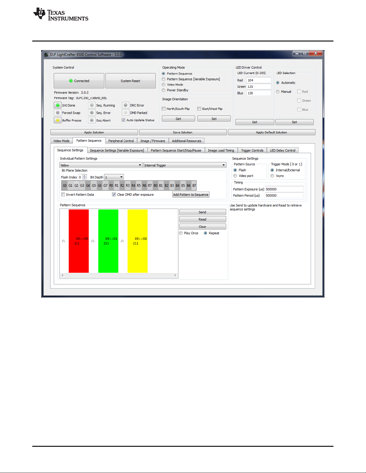
3.3 Pattern Sequence Mode
When the DLP LightCrafter 4500 is configured in Pattern Sequence mode, the DLPC350 supports 1-, 2-,
3-, 4-, 5-, 6-, 7-, and 8-bit images with a 912 columns × 1140 rows resolution. These images are pixel
accurate, meaning that each pixel corresponds to a micromirror on the DMD and is not processed by any
of the video processing functions. Three subtabs control the Pattern Sequence settings: Sequence
Settings, Pattern Sequence Start/Stop/Pause, Trigger Controls, and LED Delay Control.
3.3.1 Sequence Settings
A pattern sequence is composed of several patterns loaded from flash memory or streamed through the
24-bit RGB video port. Each individual pattern can have a specific set of LEDs illuminating it, a particular
bit-depth, and an internal or external trigger. The Sequence Settings subtab lets the user define and set all
the Individual Pattern Settings. The Trigger Controls subtab and the LED Delay Control subtab set the
trigger and LED enable edge timings, respectively. The Pattern Sequence Start/Stop/Pause tab shows the
pattern sequence validation status indicators and allows the user to play, pause and stop the
sequence.Figure 3-5 shows the DLP LightCrafter 4500 GUI with the Pattern Sequence tab selected.
30
Operating the DLP LightCrafter 4500 DLPU011E–July 2013–Revised September 2015
Copyright © 2013–2015, Texas Instruments Incorporated
Submit Documentation Feedback
Page 31
www.ti.com
Pattern Sequence Mode
Figure 3-5. DLP LightCrafter 4500 GUI – Pattern Sequence Mode
The Pattern Sequence displays images from one of the following two input sources:
• Flash: Images stored in flash memory. The flash memory can store up to sixty-four 24-bit compressed
images.
• Video port: Streamed through the Parallel RGB or FPD-link interface. Only one of these interfaces can
be connected to the DLP LightCrafter 4500 during Pattern Sequence mode.
To synchronize a camera or external system with the displayed patterns, the DLP LightCrafter 4500
supports a set of trigger inputs and outputs. These inputs and outputs are configured through the Trigger
Mode section and Trigger Controls subtab. The Trigger Mode selects the trigger input:
• Internal/External: Uses an internal trigger period to start the pattern sequence or uses the DLP
LightCrafter 4500 TRIG_IN2 signal to start and pause the pattern sequence. Each pattern in the
pattern sequence can be configured with either an internal or external trigger. With the Internal Trigger
setting, the Internal Trigger Period displays the next pattern. With External Trigger Period, the DLP
Light Crafter 4500 TRIG_IN_1 signal displays the next pattern.
• Vsync: Uses the VSYNC signal from the Parallel RGB or FPD-link interface to trigger the start of the
pattern sequence. After VSYNC, the patterns are displayed in the sequence shown on the Pattern
Sequence section. Each pattern length is determined by the Pattern Exposure time. Thus, the total
number of patterns multiplied by the pattern exposure must be less than or equal to the VSYNC period.
DLPU011E–July 2013–Revised September 2015 Operating the DLP LightCrafter 4500
Submit Documentation Feedback
Copyright © 2013–2015, Texas Instruments Incorporated
31
Page 32

Pattern Sequence Mode
Pattern sequence timing is controlled by the Pattern Period and Pattern Exposure time.
• Pattern Exposure (us): Defines the amount of time a single pattern is displayed in microseconds.
• Pattern Period (us): Defines the amount of time between patterns (in microseconds) in a pattern
sequence.
A pattern sequence can be any combination of bit depth patterns with any combination of LED sources.
The pattern sequence can be played once or continuously repeated. The allowed LED sources are:
• White: Red, green, and blue LEDs on
• Cyan: Green and blue LEDs on
• Magenta: Red and blue LEDs on
• Yellow: Red and green LEDs on
• Red: Only red LED on
• Green: Only green LED on
• Blue: Only blue LED on
To create a pattern sequence, follow these steps:
1. Choose pattern input source (Flash or Video port) from the Pattern Source section.
2. Choose Internal/External, or VSYNC trigger mode from the Trigger Mode section.
3. Set the appropriate Trigger Controls, see Section 3.3.4
4. Set the Pattern Exposure period and Pattern Period.
5. Create the pattern sequence in the Individual Pattern Settings section:
(a) Choose the LED(s) to illuminate this pattern in the pattern sequence
(b) Select the trigger for the pattern: no trigger, external positive, external negative, or internal trigger.
Internal trigger has an internal hardware signal that is input to the pattern display state machine
(meaning the controller starts displaying after receiving the signal), whereas the no internal trigger
option will display a pattern without waiting for a trigger; each pattern will display in continuation
with the previous pattern. Creating an internally triggered pattern sequence with an external trigger
input may cause unexpected behavior.
(c) Choose the Flash Index (for Flash Pattern Source) or the Frame Index (for Video port Pattern
Source) and set the bit depth for the pattern.
(i) Flash Index: This is the image's index in flash as bundled with the firmware loaded on the
LightCrafter4500. You can view the images in Video mode by changing the Input Configuration
> Source Select to Images from Flash
(ii) Frame Index: This value can be left alone. The patterns will be pulled from the specified bit-
plane(s) from each transmitted video frame sequentially
www.ti.com
32
Note: In pattern sequence mode, you are not sending a standard 24 bit RGB image, you are
sending a group of images in parallel, anywhere from 3 8-bit images (grayscale) to 24 individual 1bit images. The color for each pattern in the sequence is determined by the LEDs selected when
that pattern was added to the sequence.
(d) Select the desired pattern bit-depth to be displayed. The bit-planes are labeled G0 - G7, R0 - R7,
and B0 - B7. Clicking on a rectangle will select this bit-plane. The grouping of bit-planes is
determined by the bit-depth selected. The groupings cannot be changed. When the source is the
video port, the trigger will always be VSYNC and the VSYNC period will be the total available time
for displaying patterns (i.e. the video frame will be updated on each VSYNC). The number of
patterns that can be displayed in this time is set by the pattern exposure and pattern period times
selected.
Note that if using the video port, the incoming image resolution must be 912x1140
(e) If a black image is desired between patterns, check the Clear DMD after exposure.
(f) Click the Add Pattern to Sequence button.
(g) Repeat Steps through for each pattern in the sequence.
Operating the DLP LightCrafter 4500 DLPU011E–July 2013–Revised September 2015
Copyright © 2013–2015, Texas Instruments Incorporated
Submit Documentation Feedback
Page 33

www.ti.com
6. If the patterns sequence must be played once, set Play Once in Figure 3-5. This setting will play the
7. Clicking send will jump the GUI to the Pattern Sequence Start/Stop/Pause subtab as seen in Figure 3-
8. Pause or restart the pattern sequence through the Pause and Play buttons, respectively. If a pattern
The Pattern Sequence section in the Sequence Settings tab shows the pattern sequence as a set of
colored rectangles. The color corresponds to the LEDs used. The entries on the rectangles represent the
image source, the bit-plane, and the bit-depth as follows: S0::G0 (1) indicates flash location 0, bit-plane =
G0, bit-depth = 1. F2::G5 (3) indicates Frame 2, bit-plane = G5, bit-depth = 3. For example, in Figure 3-5,
a pattern sequence of three patterns is displayed. Each pattern is triggered every 500 ms and exposed for
500 ms. The first pattern is a 1-bit red pattern using bit-plane G0 from flash location 0. The second pattern
is a 1-bit green pattern using bit-plane G1 from flash location 0. The third pattern is a 1-bit yellow pattern
using bit-plane G2 from flash location 0.
A pulse icon in between the patterns indicates that a trigger is needed between the patterns. Right-clicking
on this icon allows the removal of the trigger, so two or more patterns can share the same trigger and are
exposed in sequence for the total exposure time. Right-clicking on a pattern allows the option of inverting
the pattern, removing the pattern, or inserting a black image by clearing the DMD after exposure time.
Pattern Sequence Mode
number of patterns set in Trigger Controls subtab under Trigger 2 Patterns per pulse. If set to 1, it
plays the first pattern in the sequence and stops. If set to 10, it plays the first 10 patterns in the
sequence. If the pattern sequence is to continuously repeat, set repeat. Make sure to click the Send
button after clicking on Play Once to download the new settings.
6. Clicking the Validate Sequence button executes a data validation and updates the Data Validation
status indicators in this tab. If the data validates successfully, the pattern sequence is downloaded to
the DLP LightCrafter 4500 and waits for the Play button to be pressed to start displaying the pattern
sequence.
If a data validation problem occurs, the appropriate status indicators are highlighted in the Data
Validation section:
• Exposure/Period OOR: When highlighted red, the Pattern Exposure period or Frame period is out
of range. The pattern exposure period must be greater than the fastest period supported, as listed
in Table 4-1.
• Pattern Number OOR: When highlighted red, the Pattern Number is out of range. The maximum
allowed patterns depend on the bit width and are listed in Table 4-1.
• Cont trig out overlaps black: When highlighted red, the continuous pattern exposure has a trigger
Out1 request or overlapping black sectors.
• Black vector missing: When highlighted red, the black vector is missing (this may also be referred
to as the post vector).
• Period, Exposure diff < 230: When highlighted red, the difference between the frame period or
internal trigger period and the exposure period of a pattern is less than 230 µs. The DMD needs
230 µs for load a pattern, so the trigger or frame period must be 230 µs greater than the pattern
exposure time.
sequence was previously loaded, the user can click the Read button to load the sequence into the GUI
window.
DLPU011E–July 2013–Revised September 2015 Operating the DLP LightCrafter 4500
Submit Documentation Feedback
Copyright © 2013–2015, Texas Instruments Incorporated
33
Page 34

Pattern Sequence Mode
www.ti.com
Figure 3-6. Pattern Sequence Mode: Start, Pause, Stop
3.3.1.1 Pattern Sequence Example
To illustrate the Pattern Sequence mode, this section describes the steps to create a sequence with
Green LED. The DLPC350 firmware has several sets of images stored in the flash memory. Flash Image
1corresponds to 24 1-bit images (vertical columns) that have been packed into a single 24-bit RGB
bitmap. To load the pattern sequence, perform the following steps:
• Select Pattern Source: Flash
• Select Pattern Trigger Mode: Internal or External
• Set Pattern Exposure: 100000 µs
• Set Pattern Period: 100000 µs
• From the Individual Pattern Settings: Select Green and Internal Trigger
• Flash Image: Select 1
• For each 24 bit-plane of the packed 24-bit RGB image, select one bit-plane (a monochrome image)
and add it to the pattern sequence by:
34
Operating the DLP LightCrafter 4500 DLPU011E–July 2013–Revised September 2015
Copyright © 2013–2015, Texas Instruments Incorporated
Submit Documentation Feedback
Page 35

www.ti.com
• This forms 24 1-bit images that are displayed back-to-back at 100-ms exposure. Click on the Send
Pattern Sequence Mode
– Clicking on G0, then clicking the Add Pattern to Sequence button
– Clicking on G1, then clicking the Add Pattern to Sequence button
– Clicking on G2, then clicking the Add Pattern to Sequence button
– Clicking on G3, then clicking the Add Pattern to Sequence button
– Clicking on G4, then clicking the Add Pattern to Sequence button
– Clicking on G5, then clicking the Add Pattern to Sequence button
– Clicking on G6, then clicking the Add Pattern to Sequence button
– Clicking on G7, then clicking the Add Pattern to Sequence button
– Clicking on R0, then clicking the Add Pattern to Sequence button
– Clicking on R1, then clicking the Add Pattern to Sequence button
– Clicking on R2, then clicking the Add Pattern to Sequence button
– Clicking on R3, then clicking the Add Pattern to Sequence button
– Clicking on R4, then clicking the Add Pattern to Sequence button
– Clicking on R5, then clicking the Add Pattern to Sequence button
– Clicking on R6, then clicking the Add Pattern to Sequence button
– Clicking on R6, then clicking the Add Pattern to Sequence button
– Clicking on R7, then clicking the Add Pattern to Sequence button
– Clicking on B0, then clicking the Add Pattern to Sequence button
– Clicking on B1, then clicking the Add Pattern to Sequence button
– Clicking on B2, then clicking the Add Pattern to Sequence button
– Clicking on B3, then clicking the Add Pattern to Sequence button
– Clicking on B4, then clicking the Add Pattern to Sequence button
– Clicking on B5, then clicking the Add Pattern to Sequence button
– Clicking on B6, then clicking the Add Pattern to Sequence button
– Clicking on B7, then clicking the Add Pattern to Sequence button
button to download the pattern sequence to the DLP LightCrafter 4500.
3.3.2 Sequence Settings [Variable Exposure]
When operating in Pattern Sequence [Variable Exposure] mode, use this subtab to set the sequence
settings. All of the sections are identical to the Sequence Settings subtab with the exception that the
Pattern Exposure time and Pattern Period are now set on a per pattern basis rather than set to the same
values for all patterns in the sequence.
DLPU011E–July 2013–Revised September 2015 Operating the DLP LightCrafter 4500
Submit Documentation Feedback
Copyright © 2013–2015, Texas Instruments Incorporated
35
Page 36

Pattern Sequence Mode
www.ti.com
Figure 3-7. Pattern Sequence Mode — Variable Exposure
3.3.3 Image Load Timing
This subtab does an instant calculation on the time the DLPC350 takes to load a full 24-bit RGB bitmap
from flash. This measurement is instantaneous and is not the average nor worst-case timing. To get an
instantaneous measurement, perform the following steps:
1. Select the desired image number from Image Index.
2. Click the Get Load Image Timing button.
The DLPC350 decompresses the 24-bit RGB bitmap stored at the Image Index location and loads it to the
internal buffer. The time required for this process is displayed in milliseconds. This feature overwrites the
images currently in the display buffer.
36
Operating the DLP LightCrafter 4500 DLPU011E–July 2013–Revised September 2015
Copyright © 2013–2015, Texas Instruments Incorporated
Submit Documentation Feedback
Page 37

www.ti.com
Pattern Sequence Mode
Figure 3-8. Image Load Timing
A typical time is 200 ms. Once an image is loaded from flash, 24 bit-fields reside in the frame buffer and
can be sequenced at higher speeds. Two 24-bit field display buffers are available in the DLPC350. If the
pattern sequence uses more than two images (48-bit fields), then approximately 200 ms is required to
load the new image into the DLPC350 internal display buffer.
3.3.4 Trigger Controls
The Trigger Controls subtab sets the polarity and adjusts the rising and falling edge delay of the trigger
inputs and outputs, see Figure 3-9. The following trigger controls are available:
• TRIG_IN_1:
– Trigger 1 In Delay: Sets the rising edge delay of the DLPC350 TRIG_IN_1 signal in relation to the
display of the pattern on the DMD. Each number adds 107.136 ns. The GUI allows for delay ranges
between 0 µs and 28084.95 µs, but for more information on how to extend the delay range, see the
DLPC350 Programmer's Guide DLPU010
• TRIG_OUT_1:
DLPU011E–July 2013–Revised September 2015 Operating the DLP LightCrafter 4500
Submit Documentation Feedback
Copyright © 2013–2015, Texas Instruments Incorporated
37
Page 38

Pattern Sequence Mode
– Trigger 1 Out Rising Edge Delay: Sets the rising edge delay of the DLPC350 TRIG_OUT_1 signal
in relation to the display of the pattern on the DMD. Each number adds 107.136 ns. Range is
–20.05 µs (before pattern exposure) to +2.79 µs (after pattern exposure) delay.
– Trigger 1 Out Falling Edge Delay: Sets the falling edge delay of the DLPC350 TRIG_IN_1 signal in
relation to the display of the pattern on the DMD. Each number adds 107.136 ns. Range is –20.05
µs (before the pattern exposure completes) to +2.79 µs (after the pattern exposure completes)
delay.
– Invert Trigger 1 Output: Sets the polarity of the TRIG_OUT_1 signal. When unchecked, the polarity
of TRIG_OUT_1 is active high. When checked, the polarity of TRIG_OUT_1 is active low.
• TRIG_OUT_2:
– Trigger 2 out Rising Edge Delay: Sets the rising edge delay of the DLPC350 TRIG_OUT_2 signal in
relation to the display of the pattern on the DMD. Each number adds 107.136 ns. Range is –20.05
µs (before pattern exposure) to +7.29 µs (after pattern exposure) delay.
– Invert Trigger 2 Output: Sets the polarity of the TRIG_OUT_2 signal. When unchecked, the polarity
of TRIG_OUT_2 is active high. When checked, the polarity of TRIG_OUT_2 is active low.
– Trigger 2 Patterns per Pulse: Indicates the number of patterns per TRIG_OUT_2 pulse.
www.ti.com
38
Figure 3-9. Trigger Control Subtab
The trigger output signals are:
Operating the DLP LightCrafter 4500 DLPU011E–July 2013–Revised September 2015
Copyright © 2013–2015, Texas Instruments Incorporated
Submit Documentation Feedback
Page 39
www.ti.com
• TRIG_OUT_1 frames the exposure time of the pattern.
• TRIG_OUT_2 indicates the start of the pattern sequence or internal buffer boundary of a 24-bit-plane.
examples of signals Figure 3-10 and Figure 3-11 show.
Pattern Sequence Mode
Figure 3-10. VSYNC Pattern Trigger Mode
Figure 3-11. External Pattern Trigger Mode
3.3.5 LED Delay Control
In Pattern Sequence mode, the LED Delay Control subtab (see Figure 3-9) sets the rising and falling edge
offsets of the LED enable signals in relation to the display of the pattern on the DMD. The rising and
falling edge of the red, green, and blue LED enable signals can be independently changed between
–20.05 µs (before pattern exposure) to +7.29 µs (after pattern exposure) delay.
When the DLP LightCrafter 4500 is operating in Video Mode, set these delays to 0 (–20.05 µs).
DLPU011E–July 2013–Revised September 2015 Operating the DLP LightCrafter 4500
Submit Documentation Feedback
Copyright © 2013–2015, Texas Instruments Incorporated
39
Page 40

Firmware Upgrade
www.ti.com
3.4 Firmware Upgrade
The DLP LightCrafter 4500 GUI allows field updates of the DLPC350 firmware. To update the DLPC350
firmware, perform the following steps Figure 3-13
1. Select the Image / Firmware tab and the Firmware Upload subtab.
2. Click the Browse button to select the file to install.
3. Click the Upload button.
4. Wait for the upload process to complete. The flash memory is erased first, then rewritten with the new
firmware image selected.
40
Operating the DLP LightCrafter 4500 DLPU011E–July 2013–Revised September 2015
Figure 3-12. LED Delay Control Subtab
Copyright © 2013–2015, Texas Instruments Incorporated
Submit Documentation Feedback
Page 41
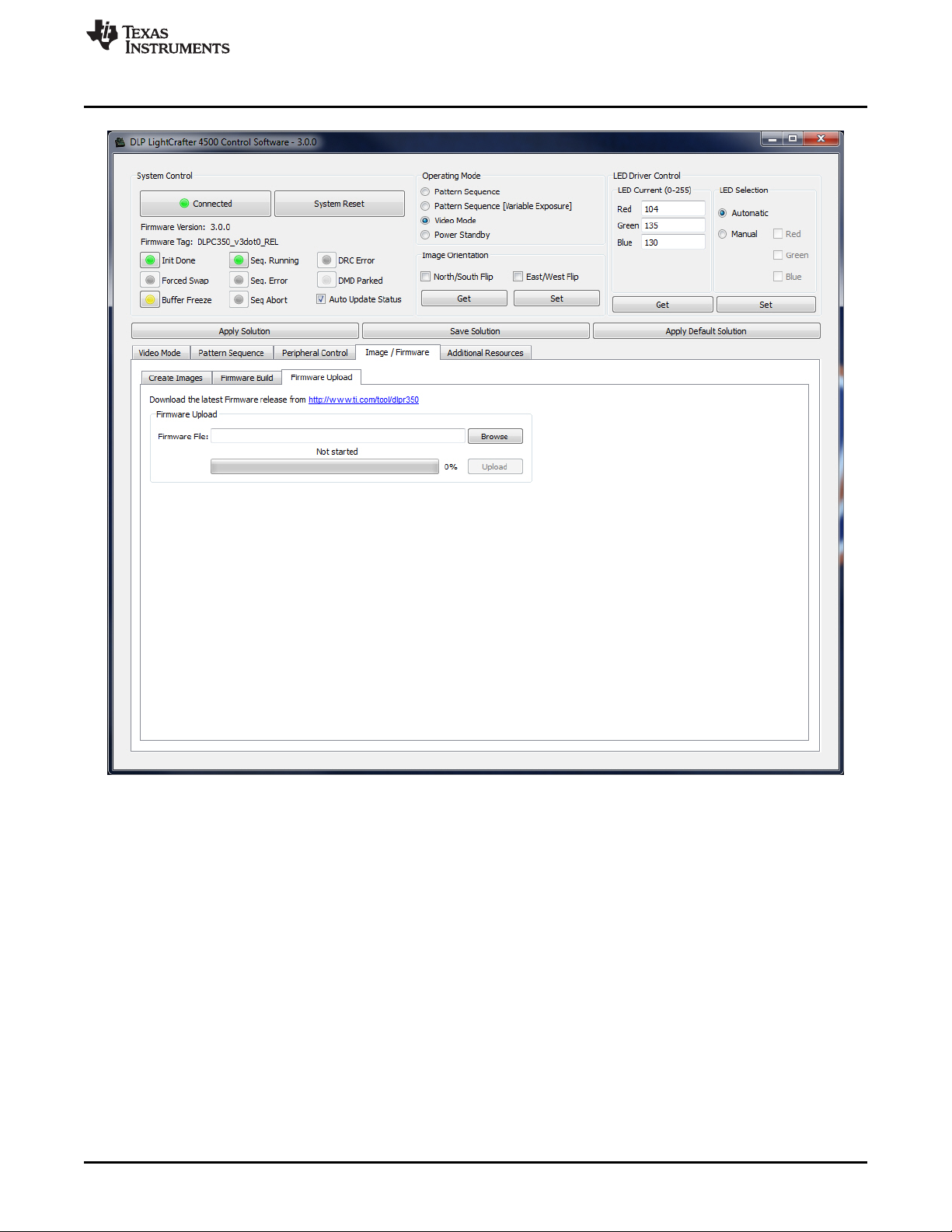
www.ti.com
Storing Images in Flash Memory
Figure 3-13. Firmware Upgrade Tab
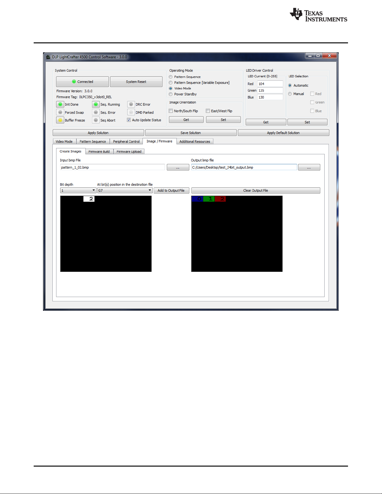
3.5 Storing Images in Flash Memory
LightCrafter 4500 allows images to be compressed and stored into the 32-MB flash memory. For most
efficient storage and compression of images, stored images are packed into groups of 24-bit RGB bitmap
images and decompressed on the fly while loaded from flash memory. To ease the packing of any bit
width images, the LightCrafter 4500 GUI offers the Create Images subtab, see Figure 3-14. To create a
24-bit image from different multiple bit depth images, perform the following steps:
1. Select the Image / Firmware tab and the Create Images subtab.
2. Select a bitmap file with 912 columns by 1140 rows by clicking the ... button next to Input bmp file
3. Select Output bitmap file by clicking the ... button next to Output bmp file
4. For an input file, add the individual bit-planes by repeating the following process:
(a) Set the bit depth and the bit field position with the Bit depth and the At bit position pulldown
selectors, respectively.
(b) Click the Add to Output File button. The current image is bit weighted and saved into the 24-bit
image of the output file.
DLPU011E–July 2013–Revised September 2015 Operating the DLP LightCrafter 4500
Submit Documentation Feedback
Copyright © 2013–2015, Texas Instruments Incorporated
41
Page 42
Storing Images in Flash Memory
www.ti.com
42
Figure 3-14. Create Images Tab
Underneath these selections, the left-hand window shows a preview of the Input file. The right-hand
window shows a preview of the 24-bit output file that has taken all the input files and bit weighted the
added images according to the bit-plane position requested. Images added at bit position B0 to B7 show
blue, bit position G0 to G7 show red, and bit position R0 to R7 show green. This is due to the DLPC350
display order being GRB (see table 2-69, Pattern Number Mapping, in the DLPC350 Programmer's
Guide), whereas BMP images are stored as RGB. For each color, bit position 0 is the least significant bit,
while bit position 7 is the most significant bit.
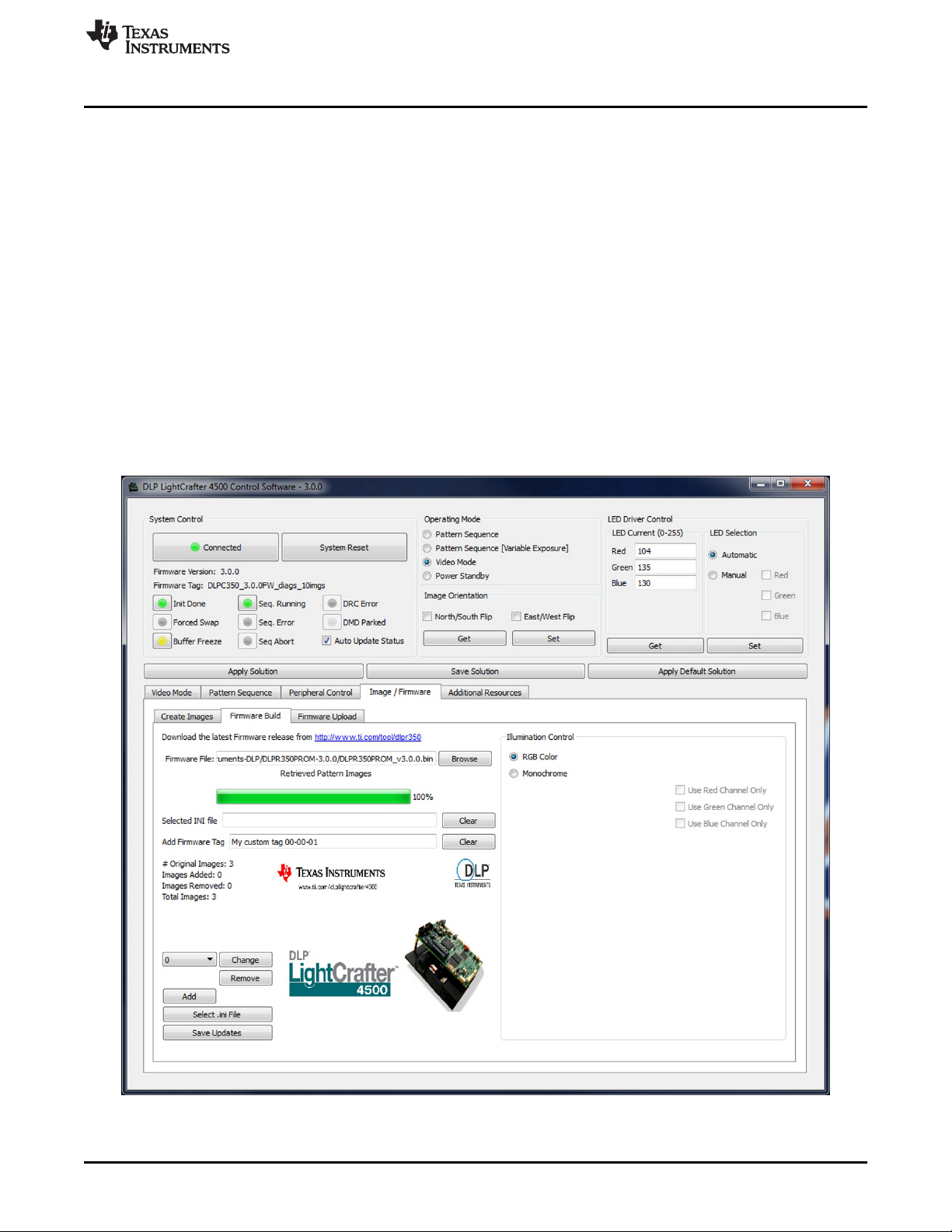
To download the images into flash, a series of 24-bit images must be added to the firmware file using the
Firmware Build subtab with the following steps:
1. Select the Image / Firmware tab and the Firmware Build subtab.
2. Select a firmware file by clicking the Browse button next to Firmware File.
3. If a new INI file is desired, refer to Section 5.2 for details on creating a custom file. Use the Select .ini
File button on the bottom left above the Save Updates button to select an existing INI file. Otherwise,
leaving this field blank will bundle the Default.ini file in the GUI top level directory with this firmware
build
Operating the DLP LightCrafter 4500 DLPU011E–July 2013–Revised September 2015
Copyright © 2013–2015, Texas Instruments Incorporated
Submit Documentation Feedback
Page 43
www.ti.com
4. Add a firmware tag. This is a 32 (or less) character string that will be associated with this firmware
5. Add 24-bit images by:
6. Choose the type of illumination control that will be used with this firmware. If you will only be using a
7. After completing the steps above, click the Save Updates button. This will prompt you for a firmware
8. Download the firmware to the LightCrafter 4500 by following the steps for the Firmware Upgrade found
After clicking Save Updates, all the 24-bit images are compressed and packed together. The number of
the image might differ from the one in the pull-down due to the packing of the 24-bit images.
Storing Images in Flash Memory
build. When the LightCrafter4500 connects to the GUI, the firmware tage is listed under the Firmware
Version in the System Control section in the top left portion of the GUI. A firmware tag is required to
build the firmware bundle.
(a) Selecting the location of the image using the pull-down, and clicking the Add button. Browse the
24-bit image file and select it. The image is displayed next to these buttons. Repeat this step to add
additional images.
single color channel, select Monochrome and check the box associated with the color channel you will
be using. Otherwise, Select the RGB Color illumination option.
final name. The name should end with .bin to ensure the GUI will find the build when browsing in the
firmware upload section. The GUI will then build and save the firmware.
in Section 3.4.
Figure 3-15. Firmware Builder
DLPU011E–July 2013–Revised September 2015 Operating the DLP LightCrafter 4500
Submit Documentation Feedback
Copyright © 2013–2015, Texas Instruments Incorporated
43
Page 44

Peripheral Control
3.6 Peripheral Control
DLPC350 offers several configurable pins. The Peripheral Control tab of the GUI controls how these pins
are configured. The following options are available:
• General Purpose Clock: Two DLPC350 pins can be individually configured as clocks.
• PWM Output Setup: Two DLPC350 pins, GPIO_00 (pin 18 in J6) and GPIO_02 (pin 22 in J6), can be
individually set as PWM outputs.
• GPIO Configuration: Several DLPC350 pins can be individually configured as GPIO. Once configured
as GPIO, the Pin Direction (Input or Output), if set to output the Pin State (High or Low) and output
type (open drain output or drive high or low), can be configured. Some GPIO pins are already
configured by the firmware for specific functions and these are listed with their current configuration.
• PWM Capture Setup: Two DLPC350 pins, GPIO_05 (pin 14 in J6) and GPIO_06 (pin 17 in J6), can be
individually set as PWM inputs. These pins will sample at the frequency specified in PWM Sample
Rate and report the duty cycle of the input signal.
• I2C0 (Master) Read/Write Control: The DLPC350 master I2C0 port can be accessed via the J16
connector on the LightCrafter4500. This section provide control over this port. The hex addresses and
data should be in the format <value><space><value><space>... For example: 0x22 0x11. The number
for bytes to be read is input as a decimal value.
www.ti.com
44
Figure 3-16. Peripheral Control Tab
Operating the DLP LightCrafter 4500 DLPU011E–July 2013–Revised September 2015
Copyright © 2013–2015, Texas Instruments Incorporated
Submit Documentation Feedback
Page 45

www.ti.com
Peripheral Control
DLPU011E–July 2013–Revised September 2015 Operating the DLP LightCrafter 4500
Submit Documentation Feedback
Copyright © 2013–2015, Texas Instruments Incorporated
45
Page 46
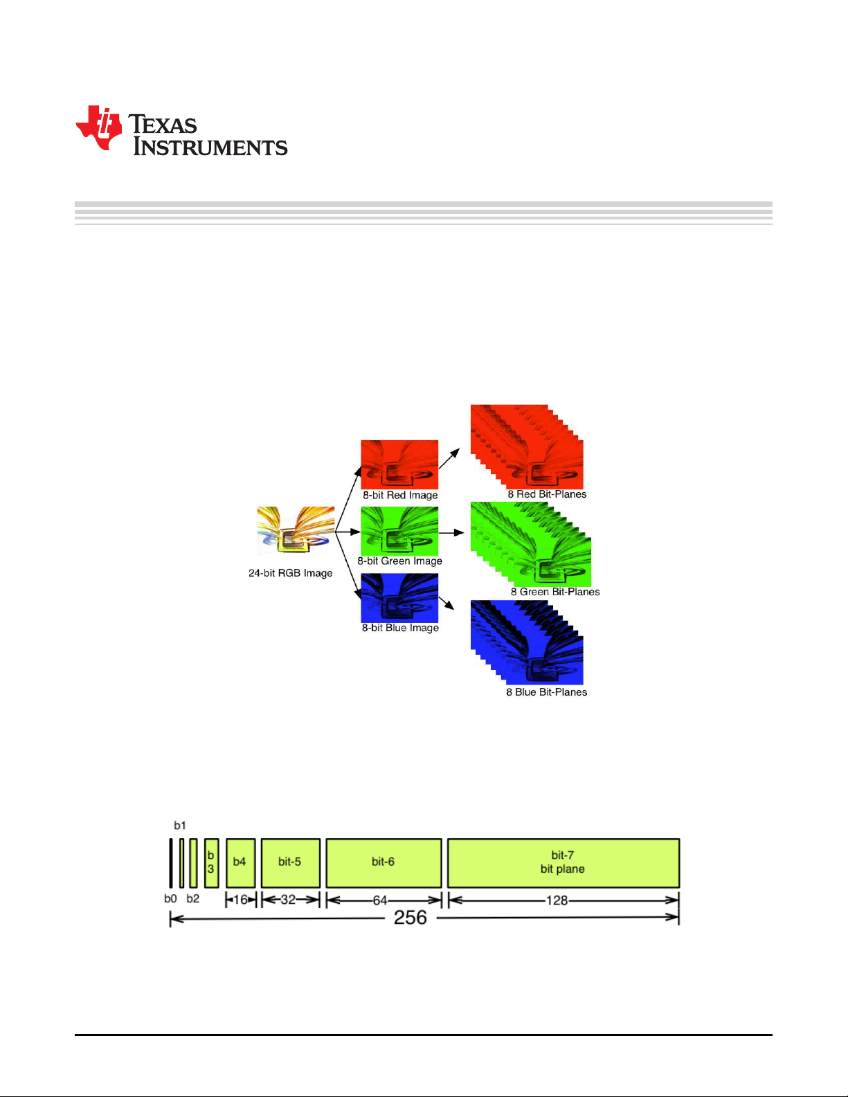
This chapter describes the pattern sequences supported by the DLP LightCrafter 4500 module.
4.1 Pattern Sequence Background
The DLPC350 takes as input 24-, 27-, or 30-bit RGB data at a frame rate of up to 120-Hz. This frame rate
is composed of three colors (red, green, and blue) with each color equally divided in the 120-Hz frame
rate. Thus, a 2.78-ms time slot is allocated to each color. Because each color has 8-, 9-, or 10-bit depth,
each color time slot is further divided into bit-planes. A bit-plane is just a 1-bit representation of all the
pixels in the image. For example, a 24-bit image is decomposed into its bit-planes in Figure 4-1.
Chapter 4
DLPU011E–July 2013–Revised September 2015
Pattern Sequences
46
Figure 4-1. Relationship Between Bit-Planes and 24-bit RGB Images
The length of each bit-plane in the time slot is weighted by the corresponding power of 2 of its binary
representation. This provides a binary pulse-width modulation of the image. For example, a 24-bit RGB
input has three colors with 8-bit depth each. Each color time slot is divided into eight bit-planes, with the
sum of all bit-planes in the time slot equal to 256. Figure 4-2 shows this partition of bits in a frame.
Figure 4-2. Bit Partition
Pattern Sequences DLPU011E–July 2013–Revised September 2015
Copyright © 2013–2015, Texas Instruments Incorporated
Submit Documentation Feedback
Page 47
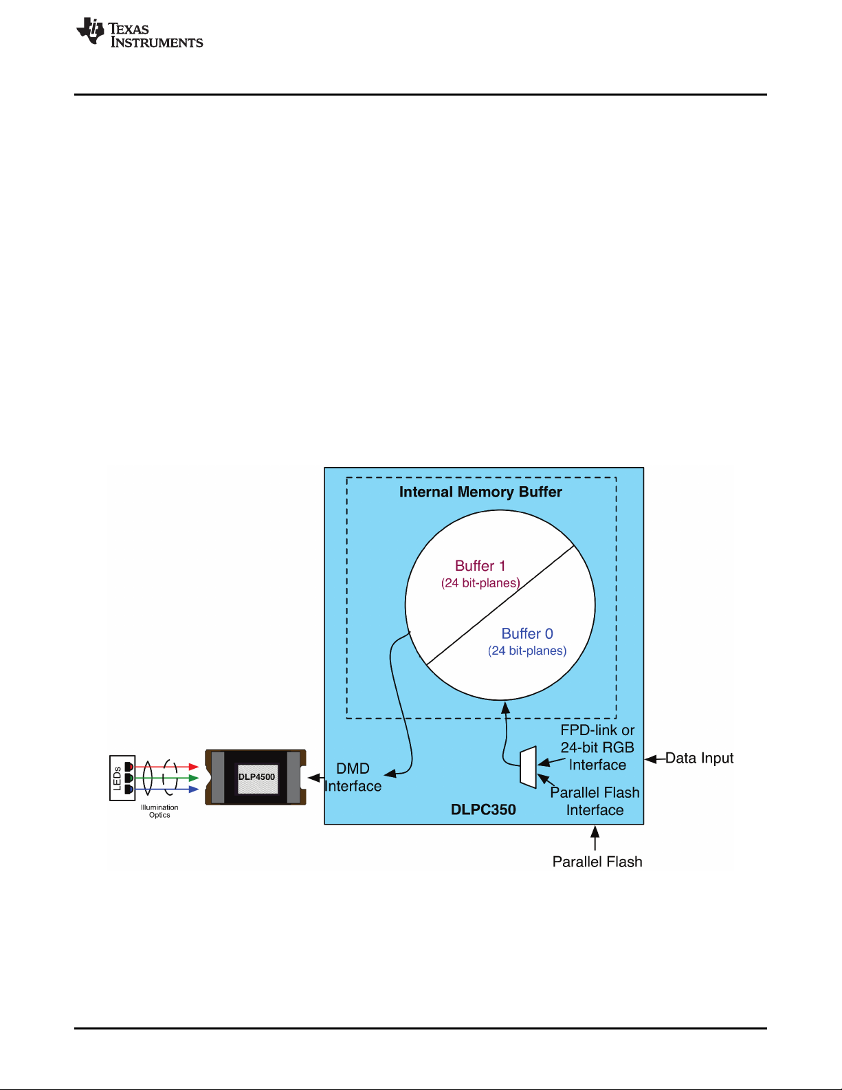
www.ti.com
Therefore, a single video frame is composed of a series of bit-planes. Because the DMD mirrors can be
either on or off, an image is created by turning on the mirrors corresponding to the bit set in a bit-plane.
With binary pulse-width modulation, the intensity level of the color is reproduced by controlling the amount
of time the mirror is on. For a 24-bit RGB frame image loaded to the DLPC350, the DLPC350 creates 24
bit-planes, stores them in its internal display buffer, and sends the bit-planes to the DLP4500 DMD, one
bit-plane at a time. Depending on the bit weight of the bit-plane, the DLPC350 controls the time this bitplane is exposed to light, controlling the intensity of the bit-plane. To improve image quality in video
frames, the bit-planes, time slots, and color frames are intertwined and interleaved with spatial-temporal
algorithms by the DLPC350.
For other applications where this image enhancement is not desired, the video processing algorithms can
be bypassed and replaced with a specific set of bit-planes. The bit depth of the pattern is then allocated
into the corresponding time slots. Furthermore, an output trigger signal is also synchronized with these
time slots to indicate when the image is displayed. For structured light applications, this mechanism
provides the capability to display a set of patterns and signals for the camera to capture these patterns
overlaid on an object.
As shown in Figure 4-3, the DLPC350 stores two 24-bit frames in its internal memory buffer. This 48 bitplane display buffer allows the DLPC350 to send one 24-bit buffer to the DMD array while the second
buffer is filled from flash or streamed in through the 24-bit parallel RGB or FPD-link interface. In streaming
mode, the DMD array displays the previous 24-bit frame while the current frame fills the second 24-bit
frame of the display buffer. Once a 24-bit frame is displayed, the buffer rotates providing the next 24-bit
frame to the DMD. Thus, the displayed image is a 24-bit frame behind the data streamed through the 24bit RGB parallel or FPD-link interface.
Pattern Sequence Background
Figure 4-3. DLPC350 Internal Memory Buffer
When the DLP LightCrafter 4500 is set to Video Mode, the displayed image is a frame delayed in relation
to the data streamed through the RGB parallel interface or FPD-link, as shown in Figure 4-4.
DLPU011E–July 2013–Revised September 2015 Pattern Sequences
Submit Documentation Feedback
Copyright © 2013–2015, Texas Instruments Incorporated
47
Page 48
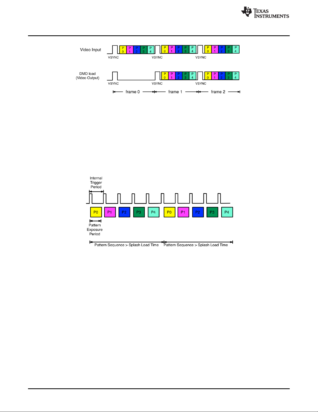
Pattern Sequence Background
Figure 4-4. Frame Delay Between Parallel Interface Input and Projection Output
When the DLP LightCrafter 4500 is set to Pattern Sequence mode with pattern source from flash, the
pattern sequence must be loaded from flash memory. The DLPC350 takes at-worst-case 200 ms to load
one buffer (24 bit-planes). The actual time to load the buffer depends on the complexity of the image. The
actual time is provided in the Image / Firmware tab under Image Load Time. If the pattern sequence is
less than 24 bit fields, the patterns are displayed from a preloaded buffer. Once the patterns are loaded,
the pattern sequence repeats from the internal display memory with no buffer load penalty. If the pattern
sequence is greater than 24 bit-fields, the 24 bit-field pattern sequence display time must be longer than
the full buffer load time. This provides enough time to load the next buffer while the current buffer is
displayed. See Figure 4-5 for a diagram of Image Load Time, Pattern Exposure Trigger period, and
Internal Trigger period.
www.ti.com
48
Figure 4-5. Image Load Time and Pattern Sequence Timing
In pattern sequence mode, the 48 bit-planes can be preloaded from flash memory and then sequenced
with a combination of patterns with different bit depths. To synchronize a camera to the displayed
patterns, the DLPC350 supports two trigger inputs and two trigger outputs. TRIG_IN_1 pulse indicates to
the DLPC350 to advance to the next pattern, while TRIG_IN_2 starts and stops the pattern sequence.
TRIG_OUT_1 frames the exposure time of the pattern, while TRIG_OUT_2 indicates the start of the
pattern sequence or internal buffer boundary of 24 bit-planes. For example, in Figure 3-10, the VSYNC
starts the pattern sequence display. The pattern sequence consists of a series of three consecutive
patterns. The first pattern sequence consists of P1, P2, and P3. P3 is an RGB pattern, it is shown with its
time-sequential representation of P3.1, P3.2, and P3.3. The second pattern sequence consists of three
patterns: P4, P5, and P6. The third sequence consists of P7, P8, and P9. TRIG_OUT_1 frames each
pattern exposed, while TRIG_OUT_2 indicates the start of each of the three pattern sequences. In
Figure 3-11, a pattern sequence of a group of four patterns are displayed. TRIG_OUT_1 frames each
pattern exposed, while TRIG_OUT_2 indicates the start of each four-pattern sequence. TRIG_IN_1 pulses
advance the pattern.
Pattern Sequences DLPU011E–July 2013–Revised September 2015
Copyright © 2013–2015, Texas Instruments Incorporated
Submit Documentation Feedback
Page 49

www.ti.com
Table 4-1 lists the allowed pattern combinations in relation to the bit depth of the external pattern.
Pattern Sequence Background
Table 4-1. Allowable Pattern Combinations
Bit Depth Input Pattern Patterns using
External RGB Number of
Rate (Hz) Two Buffers
1 bit 2880 4225 235 48
2 bits 1428 1428 700 24
3 bits 636 636 1570 16
4 bits 588 588 1700 12
5 bits 480 500 2000 8
6 bits 400 400 2500 8
7 bits 222 222 4500 6
8 bits 120 120 8333 6
Preloaded Minimum Pattern
Pattern Rate (Hz) Exposure Period (µs)
Maximum
(PreLoaded)
DLPU011E–July 2013–Revised September 2015 Pattern Sequences
Submit Documentation Feedback
Copyright © 2013–2015, Texas Instruments Incorporated
49
Page 50

Pattern Sequence Background
www.ti.com
50
Pattern Sequences DLPU011E–July 2013–Revised September 2015
Copyright © 2013–2015, Texas Instruments Incorporated
Submit Documentation Feedback
Page 51

On GUI software version 1.2 or later, any of the parameters set on the GUI can be stored as a solution.
This solution can later be recalled with a single button or set to run as default on powerup. Temporary
solutions are essentially .ini files that contain all the current parameter settings on the GUI. The .ini file is
stored on the PC. To create a new default solution, you must build the .ini file into a new firmware image.
This chapter describes the processes for creating, loading, and storing solutions.
5.1 Applying Solutions
This feature refers to the temporary solutions saved as .ini files on the PC. Three buttons in the static
panel of the GUI control the application and creation of these solutions: Apply Solution, Save Solution,
and Apply Default Solution.
• Apply Solution: Click this button to browse for .ini solutions that are already saved. Upon selecting an
.ini file, the corresponding parameters update in the GUI. Parameters the user cannot change in the
GUI (version number and splash time-out) do not take effect.
• Apply Default Solution: This button restores the settings to match those of the original DLPC350
firmware. Clicking this button is effectively the same as saving a solution and only selecting the values
in the first column of radio buttons.
• Save Solution: Click this button to make a new window with a list of several parameters (described in
Section 5.3.1) appear. One column of radio buttons contains the values set in the original DLPC350
firmware. The second column of radio buttons contains the values currently set in the GUI. The user
can select either the original or current values to store in the .ini file
Chapter 5
DLPU011E–July 2013–Revised September 2015
Saving Solutions
5.2 Changing Default Solutions
This feature refers to the process of taking an .ini file and building it into a new firmware image. The
following procedure should be followed:
1. Select the Image / Firmware tab and the Add Images to Firmware subtab.
2. Choose a base firmware file. The Select .ini File button becomes active and lets the user browse for
an .ini file.
3. Once the .ini file is selected, click the Save Updates button to save a new firmware image file.
4. Upload this new .bin or .img file to the LightCrafter 4500. The LightCrafter 4500 boots with the settings
specified in the .ini file, and returns to these settings if reset.
Before saving an .ini to firmware, TI recommends first applying the solution.
Wrong values or incorrect syntax can potentially damage the DLP LightCrafter
4500.
5.3 Modifying .ini Files
There are two ways to modify the .ini files. The first method is to use the Save Solution button on the
GUI. The second method is to open the .ini file in a text file editor and edit it manually.
5.3.1 Available Parameters
Table 5-1 lists all available parameters. For more details read the Programmer’s Guide (DLPU010).
CAUTION
DLPU011E–July 2013–Revised September 2015 Saving Solutions
Submit Documentation Feedback
Copyright © 2013–2015, Texas Instruments Incorporated
51
Page 52

Modifying .ini Files
www.ti.com
Table 5-1. List of Available Parameters when Saving Solutions
Parameter Name Programmer’s Guide Extra Notes
APPCONFIG.VERSION.SUBMINOR Retrieve Firmware Version Corresponds to: Application software patch number.
DEFAULT.AUTOSTART N/A 0x0 = Boot normally
DEFAULT.DISPMODE Display Mode Selection 0x0 = Video mode
DEFAULT.SHORT_FLIP Short-Axis Image Flip 0x0 = Disable
DEFAULT.LONG_FLIP Long-Axis Image Flip 0x0 = Disable
DEFAULT.TRIG_OUT_1.POL Trigger Out1 Control 0x0 = Active high
DEFAULT.TRIG_OUT_1.RDELAY Trigger Out1 Control Each can range from 0x00 and 0xD5
DEFAULT.TRIG OUT_1.FDELAY
DEFAULT.TRIG_OUT_2.POL Trigger Out2 Control 0x0 = Active high
DEFAULT.TRIG_OUT_2.WIDTH Trigger Out2 Control Range: 0x00 to 0xFF
DEFAULT.TRIG_IN_1.DELAY Trigger In1 Control Range: 0x00 to 0xFF
DEFAULT.TRIG_IN_2.POL Trigger In2 Control For Trigger mode 2 only
DEFAULT.RED_STROBE.RDELAY Red LED Enable Control Range: 0x00 to 0xFF
DEFAULT.RED_STROBE.FDELAY
DEFAULT.GRN_STROBE.RDELAY Green LED Enable Control Range: 0x00 to 0xFF
DEFAULT.GRN_STROBE.FDELAY
DEFAULT.BLU_STROBE.RDELAY Blue LED Enable Control Range: 0x00 to 0xFF
DEFAULT.BLU_STROBE.FDELAY
DEFAULT.INVERTDATA Pattern Display Invert Data 0x0 = Typical operation
DEFAULT.LEDCURRENT_RED LED Driver Current Control Range: 0x00 to 0xFF. On this reference design, 0x0
DEFAULT.LEDCURRENT_GRN
DEFAULT.LEDCURRENT_BLU
DEFAULT.PATTERNCONFIG.PAT_ Pattern Display Exposure and PAT_EXPOSURE must be less than PAT_PERIOD
EXPOSURE Frame Period by at least 230 µs, or it must be equal to
DEFAULT.PATTERNCONFIG.PAT_
PERIOD
DEFAULT.PATTERNCONFIG.PAT_MODE Pattern Display Data Input 0x0 = Streaming patterns through video ports
DEFAULT.PATTERNCONFIG.TRIG_ Pattern Trigger Mode 0x0 = Vsync trigger
MODE Selection 0x1 = Internal or external trigger
DEFAULT.PATTERNCONFIG.PAT_ Pattern Display LUT Control 0x0 = Play once
REPEAT 0x1 = Repeat the pattern sequence
DEFAULT.PATTERNCONFIG.NUM_ Pattern Display LUT Control Must be less than 63 (where 0x0 = 1, and 0x3F = 64).
SPLASH Must equal number of items in
DEFAULT.SPLASHLUT Pattern Display LUT Flash image indexes in the order they appear in the
DEFAULT.PATTERNCONFIG.NUM_LUT_ Pattern Display LUT Control Must be less than 128 (where 0x0 = 1, and 0x7F =
ENTRIES 128). Must equal number of items in
Command
Range: 0x0000 to 0xFFFF
0x1 = Boot in standby
0x1 = Pattern display mode (will start pattern
sequence after initialization and splash time-out)
0x1 = Enable
0x1 = Enable
0x1 = Active low
0x1 = Active low
0x1 = Inverted operation
is the maximum PWM, and 0xFF is the minimum. If
multiple LEDs are enabled simultaneously (pattern
mode or manual operation), then be mindful of
maximum current values for design.
PAT_PERIOD.
Source 0x3 = Flash memory
0x2 = Alternating trigger (not currently in GUI)
DEFAULT.SPLASHLUT
Data–Image Index pattern sequence. (Example: DEFAULT.SPLASHLUT
0x1 0x2 0x1 0x3 0x0 0x2)
DEFAULT.SEQPATLUT.
52
Saving Solutions DLPU011E–July 2013–Revised September 2015
Copyright © 2013–2015, Texas Instruments Incorporated
Submit Documentation Feedback
Page 53

www.ti.com
Modifying .ini Files
Table 5-1. List of Available Parameters when Saving Solutions (continued)
Parameter Name Programmer’s Guide Extra Notes
DEFAULT.PATTERNCONFIG.NUM_ Pattern Display LUT Control If PATTERNCONFIG.PAT_REPEAT = 0x0, then
PATTERNS should equal number of items in
DEFAULT.SEQPATLUT Pattern Display LUT Data – Example for two patterns: DEFAULT.SEQPATLUT
DEFAULT.PORTCONFIG.PORT Input Source Selection 0x0 = Parallel interface
DEFAULT.PORTCONFIG.BPP Input Source Selection 0x0 = 30-bit
DEFAULT.PORTCONFIG.PIX_FMT Input Pixel Data Format 0x0 = RGB
DEFAULT.PORTCONFIG.PORT_CLK Port Clock Select 0x0 = A (needed for this reference design)
DEFAULT.PORTCONFIG.ABC_MUX Input Data Channel Swap 0x0 – ABC = ABC
DEFAULT.PORTCONFIG.PIX_MODE FPD-Link Mode and Field 0x0 = Mode 1
DEFAULT.PORTCONFIG.SWAP_POL FPD-Link Mode and Field 0x0 = Typical
DEFAULT.PORTCONFIG.FLD_SEL FPD-Link Mode and Field 0x0 = CONT1
PERIPHERALS.I2CADDRESS[0] I2C Interface in Interface
PERIPHERALS.I2CADDRESS[1]
DATAPATH.SPLASHSTARTUPTIMEOUT N/A Time in milliseconds before default image times out.
DATAPATH.SPLASHSTARTUPENABLE N/A 0x0 = Do not show a default image when board
Command
DEFAULT.SEQPATLUT.
If PAT_REPEAT = 0x1, then should equal number of
patterns between desired Trigger Out2 pulses.
Pattern Definition 0x00042100 0x00002104;
0x1 = Internal test pattern
0x2 = Flash
0x3 = FPD-Link
0x1 = 24-bit
0x2 = 20-bit
0x3 = 16-bit
0x4 = 8-bit
0x1 = YCrCb 444
0x2 = YCrCb 422
0x1 = B
0x2 = C
Command 0x1 – ABC = CAB
0x2 – ABC = BCA
0x3 – ABC = ACB
0x4 – ABC = BAC
0x5 – ABC = CBA
Select 0x1 = Mode 2
0x2 = Mode 3
0x3 = Mode 4
Select 0x1 = Inverted
Select 0x1 = CONT2
0x2 = Force 0
Protocol Section
Range: 0x0000 to 0xFFFF
initializes (powerup or reset)
0x1 = Show a default image when board initializes
(powerup or reset)
5.3.2 Save Solution Button
When this button is clicked in the GUI, a new window with a subset of parameters from Table 5-1 appear.
One column of radio buttons contains the original values of the DLPC350 firmware. The second column of
radio buttons contains the values currently set in the GUI. Select which value or values you want in your
.ini file. This method is the preferred way of previewing syntax errors or invalid entries.
DLPU011E–July 2013–Revised September 2015 Saving Solutions
Submit Documentation Feedback
Copyright © 2013–2015, Texas Instruments Incorporated
53
Page 54

Modifying .ini Files
5.3.3 Manual Editing
The .ini files can be edited as text files. This method does not check syntax or validate commands. TI
recommends this method only for editing those commands not available through the GUI
(APPCONFIG.VERSION.SUBMINOR, DEFAULT.AUTOSTART, PERIPHERALS.I2CADDRESS,
DATAPATH.SPLASHSTARTUPTIMEOUT, and DATAPATH.SPLASHSTARTUPENABLE). This method
can be used with the LUT Helper Tool provided in the software bundle for DEFAULT.SPLASHLUT and
DEFAULT.SEQPATLUT. For more information about the tool, Section 5.3.4.
5.3.4 LUT Entry Helper Tool
The LUT Entry Helper Tool has four tabs. The first two tabs can be used to calculate the values for
DEFAULT.SEQPATLUT and DEFAULT.SPLASHLUT. The second two tabs are for reference.
5.3.4.1 Pattern LUT Entries
This tab is used to calculate the values for DEFAULT.SEQPATLUT. The table with 128 possible entries
can be modified with the desired parameters for each pattern in the pattern sequence. It is possible to
customize various parameters for each pattern. Valid entries for each category below are found in the
Data tab.
• BIT-DEPTH: Select between 1 and 8.
• PATTERN: Select the desired pattern number. Each bit-depth of n corresponds to a pattern number
equal to 24 / n. See the Pattern Bit-Planes tab to understand the mapping of bit-planes to pattern
number.
• LED: Select which LEDs are on.
• TRIG IN: Select the type of trigger input that will trigger the current pattern. If streaming through the
video port, the VSYNC acts as the External Positive trigger, and any subsequent patterns in the frame
(between VSYNC pulses) have no trigger. These patterns are labeled with Continue in the Pattern
Sequence window.
• PAT INVERT: Select whether or not to invert the pattern.
• INSERT BLK: Select whether to clear the DMD after each pattern or not. TI recommends clearing the
DMD at least after the last pattern in the LUT.
• BUFF SWAP: This parameter indicates whether or not to move to the next flash image in the
SPLASHLUT. Each time this is a yes, the SPLASHLUT index increments. The index returns to 0 if
there are no more indexes.
• TRIG OUT: Either a new Trigger Out1 is generated (NEW) or the pattern shares exposure time with
the previous pattern (PREV) and no output trigger is generated.
As the user changes the values in the LUT, the values in the LUT DATA column change. After entering
the parameters for as many patterns as needed, scroll to the bottom of the sheet. Enter the total number
of patterns next to N = (in cell C138). Then, row 139 generates the necessary values the user must copy
into the .ini file.
Lastly, there is a Debug Helper tool at the bottom of this sheet. Enter a hex code where it says LUT DATA
to find out what the corresponding parameters are.
www.ti.com
5.3.4.2 Image LUT Entries
This tab is used to calculate the values for DEFAULT.SPLASHLUT. This tab converts the desired image
indexes into hexadecimal values. Row 6 contains the calculated string of values for your .ini file. If the
user repeats indexes, enter them separately. See this example in Table 5-2; the order is 0, 13, 12, 1, 13,
12, 0, 13, 12, 1, 13, 12, and so on.
SL No. 1 2 3 4 5 6
Image Index in Decimal 0 13 12 1 13 12
DEFAULT.SPLASHLUT 0x0 0xD 0xC 0x1 0xD 0xC
54
Saving Solutions DLPU011E–July 2013–Revised September 2015
Table 5-2. Image LUT Entries Example
Copyright © 2013–2015, Texas Instruments Incorporated
Submit Documentation Feedback
Page 55

www.ti.com
Modifying .ini Files
DLPU011E–July 2013–Revised September 2015 Saving Solutions
Submit Documentation Feedback
Copyright © 2013–2015, Texas Instruments Incorporated
55
Page 56

This chapter describes the interface between the DLP LightCrafter 4500 and the PandaBoard ES.
6.1 PandaBoard 4500
PandaBoard ES is a low-cost, open-development platform based on the TI OMAP4 application processor.
The PandaBoard ES is supported by a dedicated community at PandaBoard.org. The DLP LightCrafter
4500 combined with a PandaBoard ES provides users with an embedded platform that eliminates the
need for a dedicated laptop or PC. The PandaBoard ES includes an OMAP4 1.2-GHz, dual-core
processor, 1GB of onboard RAM, SD card slot, and a suite of connectivity options, including:
• Ethernet, Bluetooth
• Wi-Fi
• USB 2.0
• HDMI output and a camera input connector.
The combination of PandaBoard ES with DLP LightCrafter 4500 allows for the creation of self-contained,
high-precision mobile tools to meet a growing number of applications, such as inline machine vision
systems, portable, high-accuracy 3D scanners, and field spectrometers.
To interface a PandaBoard ES with the DLP LightCrafter 4500, the following modifications are needed:
• Populate J1 with Samtec FW-10-04-F-D-570-140
• Populate J3 with Samtec ZW-14-10-F-D-415-200
• Populate J4 with Samtec FW-10-04-F-D-570-140
• Populate J6 with Samtec ZW-14-10-F-D-415-200
• Remove resistor R152 on the PandaBoard ES. The DLP LightCrafter 4500 powers the PandaBoard.
Removing the resistor prevents the PandaBoard from being powered by the USB and conflicting with
the DLP LightCrafter 4500 power.
• Add four metric male-female threaded hex standoffs with a length of 19 mm and a M3 screw size
Due to the tight tolerances in the J1, J3, J4, and J6 connectors alignment, TI recommends inserting these
headers on the corresponding DLP LightCrafter 4500 connector before soldering. For ease of use,
SVTronics®has created a custom-build option of the PandaBoard ES that includes the connectors and
standoffs, and removes the R152 resistor, called PandaBoard 4500. Figure 6-1 shows a DLP LightCrafter
4500 with a PandaBoard 4500.
Chapter 6
DLPU011E–July 2013–Revised September 2015
PandaBoard Interface
®
56
PandaBoard Interface DLPU011E–July 2013–Revised September 2015
Copyright © 2013–2015, Texas Instruments Incorporated
Submit Documentation Feedback
Page 57

www.ti.com
PandaBoard 4500
Figure 6-1. DLP LightCrafter 4500 With PandaBoard 4500
6.1.1 DLP LightCrafter 4500 to PandaBoard Interface
As shown in Figure 6-2, the DLP LightCrafter 4500 supplies 5-V power to the PandaBoard. The
PandaBoard provides 1.8 V to the DLP LightCrafter 4500 to level-shift all the signals interfacing the two
boards together. The following OMAP4 GPIOs control the routing of OMAP4 peripherals to the
corresponding DLPC350 peripherals:
• To power down the output of TFP401 and enable the level shifters in the 24-bit RGB interface, the
OMAP4 processor must drive GPIO_140 (SYS_MSTR_MUX_SEL) high.
• To connect the OMAP4 USB3 bus to the DLC350, OMAP4 must drive GPIO_39 (SYS_USB_SEL)
high.
• To connect the OMAP4 I2C2 bus to the DLPC350 I2C1 bus, OMAP4 must drive GPIO_51
(SYS_I2C_OE) high.
• To disconnect UART output of DLPC350 from J20 and route it to OMAP4 UART4, OMAP4 must drive
GPIO_33 high.
• To connect the triggers from DLPC350 to OMAP4 GPIOs, OMAP4 must drive GPIO_61
(SYS_TRIGGER_SEL) high.
Table 6-1, Table 6-2, Table 6-3, and Table 6-4 list the signals interfacing the OMAP4 processor in the
PandaBoard 4500 with the DLPC350 in the DLP LightCrafter 4500.
DLPU011E–July 2013–Revised September 2015 PandaBoard Interface
Submit Documentation Feedback
Copyright © 2013–2015, Texas Instruments Incorporated
57
Page 58
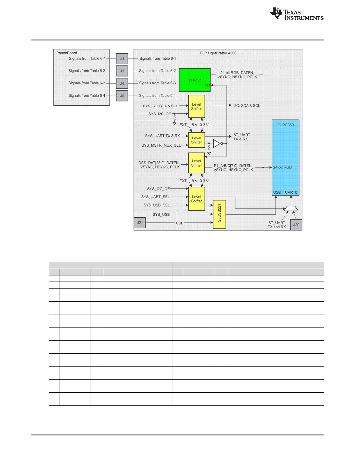
PandaBoard 4500
www.ti.com
Figure 6-2. Block Diagram of the PandaBoard Interface
Table 6-1. J1 PandaBoard 4500 to DLP LightCrafter 4500 Interface
PandaBoard 4500 J1 DLP LightCrafter 4500 J1
Pin Signal I/O Description Pin Signal I/O Description
1 DCIN_JACK PWR 5 V supplied from DLP LightCrafter 4500 1 PP5P0V PWR 5 V supplied by TLV62130 (U28) of DLP LightCrafter 4500
2 DCIN_JACK PWR 5 V supplied from DLP LightCrafter 4500 2 PP5P0V PWR 5 V supplied by TLV62130 (U28) of DLP LightCrafter 4500
3 h_DSS_DAT1 O OMAP4 LCD pixel data bit 1 3 SYS_DATA01 I DLPC350 P1_A_3 level-shifted to 1.8 V
4 h_DSS_DAT0 O OMAP4 LCD pixel data bit 0 4 SYS_DATA00 I DLPC350 P1_A_2 level-shifted to 1.8 V
5 h_DSS_DAT3 O OMAP4 LCD pixel data bit 3 5 SYS_DATA03 I DLPC350 P1_A_5 level-shifted to 1.8 V
6 h_DSS_DAT2 O OMAP4 LCD pixel data bit 2 6 SYS_DATA02 I DLPC350 P1_A_4 level-shifted to 1.8 V
7 h_DSS_DAT5 O OMAP4 LCD pixel data bit 5 7 SYS_DATA05 I DLPC350 P1_A_7 level-shifted to 1.8 V
8 h_DSS_DAT4 O OMAP4 LCD pixel data bit 4 8 SYS_DATA04 I DLPC350 P1_A_6 level-shifted to 1.8 V
9 h_DSS_DAT12 O OMAP4 LCD pixel data bit 12 9 SYS_DATA12 I DLPC350 P1_B_6 level-shifted to 1.8 V
10 h_DSS_DAT10 O OMAP4 LCD pixel data bit 10 10 SYS_DATA010 I DLPC350 P1_B_4 level-shifted to 1.8 V
11 h_DSS_DAT23 O OMAP4 LCD pixel data bit 23 11 SYS_DATA23 I DLPC350 P1_C_9 level-shifted to 1.8 V
12 h_DSS_DAT14 O OMAP4 LCD pixel data bit 14 12 SYS_DATA14 I DLPC350 P1_B_8 level-shifted to 1.8 V
13 h_DSS_DAT19 O OMAP4 LCD pixel data bit 19 13 SYS_DATA19 I DLPC350 P1_C_5 level-shifted to 1.8 V
14 h_DSS_DAT22 O OMAP4 LCD pixel data bit 22 14 SYS_DATA22 I DLPC350 P1_C_8 level-shifted to 1.8 V
15 H_I2C2_SDA I/O OMAP4I2C2 serial data 15 SYS_I2C1_SDA I/O DLPC350 I2C1_SDA level-shifted to 1.8 V
16 h_DSS_DAT11 O OMAP4 LCD pixel data bit 11 16 SYS_DATA11 I DLPC350 P1_B_5 level-shifted to 1.8 V
17 h_DSS_VSYNC O OMAP4 LCD vertical sync signal 17 SYS_VSYNC I DLPC350 P1_VSYNC level-shifted to 1.8 V
18 H_DPM_EMU2 I DPM_EMU2/GPIO_13 18 NC No connect
19 GND GND Ground bus 19 GND GND Ground bus
20 GND GND Ground bus 20 GND GND Ground bus
58
PandaBoard Interface DLPU011E–July 2013–Revised September 2015
Copyright © 2013–2015, Texas Instruments Incorporated
Submit Documentation Feedback
Page 59

www.ti.com
PandaBoard 4500
Table 6-2. J3 PandaBoard 4500 to DLP LightCrafter 4500 Interface
PandaBoard 4500 J3 DLP LightCrafter 4500 J3
Pin Signal I/O Description Pin Signal I/O Description
1 VIO_1V8 PWR Panda 1.8-V system I/O voltage 1 EXT_1V8 PWR 1.8 V supplied by Panda
2 DCIN_JACK PWR 2 PP5P0V PWR
3 GPMC_AD7 I/O 3 NC No connect
MCSPI1_CS3 / OMAP4 SPI1 chip select 3 (also the RGB signals to DLPC350, and disables TFP401.
4 O 4 SYS_MASTER_MUX_SEL I
GPIO_140 UART1_RTS) When low, RGB signals are muxed to TFP401 and
5 GPMC_AD6 I/O 5 NC No connect
6 UART4_TX O OMAP4 UART4 transmit data 6 SYS_UART0_RX I DLPC350 UART0_RX level-shifted to 1.8 V
7 GPMC_AD5 I/O 7 NC No connect
8 UART4_RX I OMAP4 UART4 receive data 8 SYS_UART0_TX0 O
9 GPMC_AD4 I/O 9 NC No connect
MCSPI1_CS1 / OMAP4 SPI1 chip select 1 (also
10 O 10 SYS_TRIG_IN_1 I signal advances the pattern during Pattern
GPIO_138 UART1_RX)
11 GPMC_AD3 I/O 11 NC No connect
MCSPI1_SIMO /
12 I/O OMAP4 SPI1 slave in master out 12 SYS_TRIG_IN_2 I signal is used as a start (rising edge) or stop (falling
GPIO_136
13 GPMC_AD2 I/O 13 NC No connect
MCSPI1_CS2 / OMAP4 SPI1 chip select 2 (also
14 O 14 DRV_EXT_POWER_ON O Thissignal indicates to OMAP4 the DLPC350 is
GPIO_139 UART1_CTS)
15 GPMC_AD1 I/O 15 NC No connect
MCSPI1_CS0 /
16 I/O OMAP4 SPI1 chip select 0 16 DRV_TRIG_OUTB_2 O DLPC350 active high signal to indicate first pattern
GPIO_137
17 GPMC_AD0 I/O 17 NC No Connect
MCSPI1_SOMI /
18 I/O OMAP4 SPI1 slave out master I 18 DRV_TRIG_OUTB_1 O DLPC350active high pattern exposure signal during
GPIO_135
19 GPMC_NWE O OMAP4 GPMC write enable 19 NC No connect
MCSPI1_CLK /
20 I/O OMAP4SPI1 clock out 20 DRV_INIT_DONE O DLPC350active high pulse signal to indicate system
GPIO_134
21 GPMC_NOE O OMAP4 GPMC output enable 21 NC No connect
GPMC_AD15 / OMAP4 GPMC address or data When low, driver board USB connector is routed to
22 I/O 22 SYS_USB_SEL I
23 I2C4_SDA I/O OMAP4 I2C4 serial data 23 NC No connect
24 I2C4_SCL O OMAP4 I2C4 serial clock 24 NC No connect
25 REGEN1 O Panda TWL6030 REGEN1 25 NC No connect
26 SYS_NRESPWRON O Panda power-on reset 26 NC No connect
27 DGND GND Digital ground 27 GND GND Digital ground
28 DGND GND Digital ground 28 GND GND Digital ground
GPIO_39 bit 15 DLPC350. When high, OMAP4 drives USB to
5 V supplied from DLP 5 V supplied by TLV62130 (U28) of DLP
LightCrafter 4500 LightCrafter 4500
OMAP4 GPMC address or data
OMAP4GPMC address or data
OMAP4 GPMC address or data
OMAP4 GPMC address or data
OMAP4GPMC address or data
OMAP4 GPMC address or data
OMAP4 GPMC address or data
OMAP4 GPMC address or data
bit 7
bit 6
bit 5
bit 4
bit 3
bit 2
bit 1
bit 0
When high, Panda enables the level shifters, muxes
level shifters to Panda are disabled.
DLPC350 UART0_TX level-shifted to 1.8 V. Outputs
DLPC350 TRIG_IN_1 level-shifted to 1.8 V. This
DLPC350 TRIG_IN_2 level-shifted to 1.8 V. This
DLPC350 EXT_POWER_ON level-shifted to 1.8 V.
Signal from OMAP4 to switch the TS3USB221 mux.
error info from DLPC350.
Sequence mode.
edge) during Pattern Sequence mode.
powered ON.
DLPC350 TRIG_OUT_2 level-shifted to 1.8 V.
in Pattern Sequence mode.
DLPC350 TRIG_OUT_2 level-shifted to 1.8 V.
Pattern Sequence mode.
DLPC350INTI_DONE level-shifted to 1.8 V.
initialization is complete.
DLPC350.
DLPU011E–July 2013–Revised September 2015 PandaBoard Interface
Submit Documentation Feedback
Copyright © 2013–2015, Texas Instruments Incorporated
59
Page 60
PandaBoard 4500
www.ti.com
Table 6-3. J4 PandaBoard 4500 to DLP LightCrafter 4500 Interface
PandaBoard 4500 J4 DLP LightCrafter 4500 J4
Pin Signal I/O Description Pin Signal I/O Description
1 VDD_V AUX2 PWR 1 NC No connect
2 VIO_1V8 PWR Panda 1.8 V system I/O voltage 2 EXT_1V8 PWR 1.8 V supplied by Panda
3 h_DSS_DAT20 O OMAP4 LCD pixel data bit 20 3 SYS_DATA20 I DLPC350 P1_C_6 level-shifted to 1.8 V
4 h_DSS_DAT21 O OMAP4 LCD pixel data bit 21 4 SYS_DATA21 I DLPC350 P1_C_7 level-shifted to 1.8 V
5 h_DSS_DAT17 O OMAP4 LCD pixel data bit 17 5 SYS_DATA17 I DLPC350 P1_C_3 level-shifted to 1.8 V
6 h_DSS_DAT18 O OMAP4 LCD pixel data bit 18 6 SYS_DATA18 I DLPC350 P1_C_4 level-shifted to 1.8 V
7 h_DSS_DAT15 O OMAP4 LCD pixel data bit 15 7 SYS_DATA15 I DLPC350 P1_B_9 level-shifted to 1.8 V
8 h_DSS_DAT16 O OMAP4 LCD pixel data bit 16 8 SYS_DATA16 I DLPC350 P1_C_2 level-shifted to 1.8 V
9 h_DSS_DAT7 O OMAP4 LCD pixel data bit 7 9 SYS_DATA7 I DLPC350 P1_A_9 level-shifted to 1.8 V
10 h_DSS_DAT13 O OMAP4 LCD pixel data bit 13 10 SYS_DATA13 I DLPC350 P1_B_7 level-shifted to 1.8 V
11 h_DSS_DAT8 O OMAP4 LCD pixel data bit 8 11 SYS_DATA8 I DLPC350 P1_B_2 level-shifted to 1.8 V
12 NUSB_PWR O Input power enable 12 NC No connect
13 h_DSS_DAT9 O OMAP4 LCD pixel data bit 9 13 SYS_DATA09 I DLPC350 P1_B_3 level-shifted to 1.8 V
14 H_I2C2_SCL O OMAP4 I2C2 serial clock 14 SYS_I2C1_SCL I DLPC350 I2C1_SCL level-shifted to 1.8 V
15 h_DSS_DAT6 I/O OMAP4 LCD pixel data bit 6 15 SYS_DATA06 I/O DLPC350 P1_A_8 level-shifted to 1.8 V
16 h_DSS_PCLK O OMAP4 LCD pixel clock 16 SYS_PCLK I DLPC350 P1_CLK level-shifted to 1.8 V
17 h_DSS_DEN O OMAP4 LCD data enable 17 SYS_DATA_EN I DLPC350 P1_DATAEN level-shifted to 1.8 V
18 h_DSS_HSYNC O OMAP4 LCD horizontal sync 18 SYS_HSYNC I DLPC350 P1_HSYNC level-shifted to 1.8 V
19 GND GND Ground bus 19 GND GND Digital ground
20 GND GND Ground bus 20 GND GND Digital ground
Panda power rail
(adjustable from 1.2 V to 2.8 V)
Table 6-4. J6 PandaBoard 4500 to DLP LightCrafter 4500 Interface
PandaBoard 4500 J6 DLP LightCrafter 4500 J6
Pin Signal I/O Description Pin Signal I/O Description
1 VBUS_3 PWR 1 NC No connect
2 VBUS_4 PWR 2 NC No connect
3 USBH3_DM I/O OMAP4 USB host port 3 data minus 3 SYS_USB_DN I/O TS3USB221 USB DN
4 USBH4_DM I/O OMAP4 USB host port 4 data minus 4 NC No connect
5 USBH3_DP I/O OMAP4 USB host port 3 data plus 5 SYS_USB_DP I/O TS3USB221 USB DP
6 USBH4_DP I/O OMAP4 USB host port 4 data plus 6 NC No connect
7 DGND GND Digital ground 7 GND GND Digital ground
8 DGND GND Digital ground 8 GND GND Digital ground
GPMC_AD14 / DLPC350 GPIO11 (ClockC output) level-shifted
9 I/O OMAP4 GPMC address or data bit 14 9 DRV_GPIO11 O
GPIO_38 to 1.8 V
GPMC_AD13 / DLPC350 GPIO12 (ClockD output) level-shifted
10 I/O OMAP4 GPMC address or data bit 13 10 DRV_GPIO12 O
GPIO_37 to 1.8 V
SYS_NRESWA
11 I/O Panda Warm Reset 11 NC No connect
12 I Power on input to TWL6030 (ref. to VBAT) 12 NC No connect
13 HFL_P O Hands free left speaker out (+) 13 NC No connect
14 _PWM / O OMAP4 display PWM control 14 SYS_GPIO5 I
15 HFL_N O Hands free left speaker out (–) 15 NC No connect
16 VDD_V AUX1 PWR TWL6030 VAUX1 16 NC No connect
17 I/O OMAP4 GPMC address or data bit 13 17 SYS_GPIO6 I
18 I/O OMAP4 GPMC address or data bit 8 18 DRV_GPIO00 O
19 I OMAP4 GPMC Wait input 0 19 SYS_TRIGGER_SEL I
20 I/O OMAP4 GPMC address or data bit 9 20 SYS_UART_SEL I
RM
PB_POWER_O
N
H_DMTIMER11
GPIO121
GPMC_AD12 / DLPC350 GPIO6 (PWM1 input) level-shifted to
GPIO_36 1.8 V
GPMC_AD8 / DLPC350 GPIO0 (PWM0 output) level-shifted to
GPIO_32 1.8 V
GPMC_W AIT0 / Pandaboard. When low routes DLPC350 trigger
GPIO_61 Inputs to DLP LightCrafter 4500 input trigger
GPMC_AD9 / Pandaboard. When low routes the DLPC350
GPIO_33 UART to the DLP LightCrafter 4500 UART
OMAP4 VBUS output from USB Host Port
OMAP4 VBUS output from USB Host Port
#3
#4
DLPC350 GPIO5 (PWM0 input) level-shifted to
When high routes DLPC350 trigger inputs to
When high routes the DLPC350 UART to
1.8 V
connector.
connector.
60
PandaBoard Interface DLPU011E–July 2013–Revised September 2015
Submit Documentation Feedback
Copyright © 2013–2015, Texas Instruments Incorporated
Page 61

www.ti.com
Table 6-4. J6 PandaBoard 4500 to DLP LightCrafter 4500 Interface (continued)
PandaBoard 4500 J6 DLP LightCrafter 4500 J6
Pin Signal I/O Description Pin Signal I/O Description
GPMC_NWP /
21 O OMAP4 GPMC write protect 21 NC No connect
GPIO_54
GPMC_AD10 / DLPC350 GPIO2 (PWM2 output) level-shifted to
22 I/O OMAP4 GPMC address or data bit 10 22 DRV_GPIO02 O
GPIO_34 1.8 V
GPMC_CLK /
23 O OMAP4 GPMC Clock Out 23 NC No connect
GPIO_55
GPMC_AD11 / External Trigger Input from connector J11
24 I/O OMAP4 GPMC address or data bit 11 24 DRV_TRIG_OUTA_1 O
GPIO_35 TRIG1_IN_CONN level-shifted to 1.8 V
GPMC_NCS0 / External Trigger Input from connector J11
25 O OMAP4 GPMC chip select 0 25 DRV_TRIG_OUTA_2 O
GPIO_50 TRIG2_IN_CONN level-shifted to 1.8 V
GPMC_NADV_ OMAP4GPMC address valid or address
26 O 26 NC No connect
ALE / GPIO_56 latch enable
GPMC_NCS1 /
27 O OMAP4 GPMC chip select 1 27 SYS_I2C_OE I DLPC350 I2C1 bus. When low, disconnects the
GPIO_51
GPMC_NBE0_ OMAP4 GPMC byte enable 0 or command
28 O 28 NC No connect
CLE / GPIO_59 latch enable
6.1.2 PandaBoard Software
Note: Only up to revision B2 of the PandaBoard are officially supported
The HDMI connector is the default display output of PandaBoard. To reroute the display video output to
the RGB interface of the DLP LightCrafter 4500, the kenrel config file must be modified with the following
changes:
• Disable DRM
• Enable DVI output
• Enable frame buffer support
To perform these changes, obtain the Ubuntu®kernel from the repository:
• git clone git://kernel.ubuntu.com/ubuntu/ubuntu-precise.git
• git checkout -b working origin/ti-omap4
Install ARM compilers on Linux®machine:
• sudo apt-get install gcc-arm-linux-gnueabihf cpp-arm-linux-gnueabihf
• sudo apt-get install gcc-arm-linux-gnueabi cpp-arm-linux-gnueabi
To run the menuconfig, install ncurses package:
• sudo apt-get install build-essential ncurses-dev
Before compiling the Ubuntu kernel, the DVI port must be enabled. Run menuconfig:
• cp debian.ti-omap4/config/config.common.ubuntu.config
• sudo make ARCH=arm menuconfig
Select the following:
• Disable DRM under: Device Drivers → Graphics Support → Direct Rendering Manager
• Enable DVI under: Device Drivers → Graphic Support → OMAP2+ Display Subsystem support →
OMAP2/3 Display Device Drivers → DVI Output
• Enable frame buffer support: Device Drivers → Graphic Support → OMAP2+ Display Subsystem
support → OMAP2+ frame buffer support
Build the kernel:
• ARCH=arm CROSS_COMPILE=arm-linux-gnueabi- make
Generate the uImage:
• ARCH=arm CROSS_COMPILE=arm-linux-gnueabi- make uImage
The generated uImage will be located at ubuntu-precise/arch/arm/boot/uImage.
PandaBoard 4500
When high, connects the OMAP4 I2C2 bus to
OMAP4 I2C2 bus from the DLPC350 I2C1 bus.
DLPU011E–July 2013–Revised September 2015 PandaBoard Interface
Submit Documentation Feedback
Copyright © 2013–2015, Texas Instruments Incorporated
61
Page 62

PandaBoard 4500
To configure the OMAP4 LCD peripheral drive for the DLP LightCrafter 4500 24-bit RGB input, perform
the following changes to the boot script. The boot script, boot.scr, is used by U-Boot.
• Set the DVI as the default output by adding the following entry to boot.scr:
– omapfb.mode=dvi omapdss.def_disp=dvi
• Set the desired resolution fro the DLP LightCrafter 4500 output by adding one of the following entries
to boot.scr:
– omapfb.mode=dvi:912x1140MR-24@60
– omapfb.mode=dvi:1280x800MR-24@60
• Generate the boot.scr:
– mkimage -A arm -T script -C none -n "Boot Image" -d boot.script boot.scr
• Copy the generated uImage and boot.scr in the boot partition of the SD card.
Make the modules:
• Make CROSS_COMPILE=arm-linux-gnueabi- ARCH=arm INSTALL_MOD_PATH=<path_of_modules>
modules_install
Copy the ‘modules’ folder from the path given in the previous command to the \lib folder on secondary
partition.
www.ti.com
62
PandaBoard Interface DLPU011E–July 2013–Revised September 2015
Copyright © 2013–2015, Texas Instruments Incorporated
Submit Documentation Feedback
Page 63

www.ti.com
PandaBoard 4500
DLPU011E–July 2013–Revised September 2015 PandaBoard Interface
Submit Documentation Feedback
Copyright © 2013–2015, Texas Instruments Incorporated
63
Page 64

This chapter describes the connector pins of the DLP LightCrafter 4500 module.
7.1 Input Trigger Connectors
Table 7-1 lists the input trigger connector (J11) pins. The trigger inputs have hysteresis. Two matching sixpin, 1.25-mm connector part numbers are:
• Molex part number: 51021-0600
• Digi-Key part number: WM1724-ND
The corresponding connector terminal (crimp) part numbers are:
• Molex part number: 50079-8100
• Digi-Key part number: WM2023-ND
Description Pin Supply Range
Trigger In 1 supply 1
Trigger In 1 2
Ground 3 Ground
Trigger In 2 supply 4
Trigger In 2 5
Ground 6 Ground
Chapter 7
DLPU011E–July 2013–Revised September 2015
Connectors
Table 7-1. Input Trigger Connector Pins
External or internal 1.8-V and 3.3-V
selectable at J10
External or internal 1.8-V and 3.3-V
selectable at J12
7.2 Output Trigger Connectors
Table 7-2 lists the output trigger connector (J14) pins. Two matching six-pin, 1.25-mm connector part
numbers are:
• Molex part number: 51021-0600
• Digi-Key part number: WM1724-ND
The corresponding connector terminal (crimp) part numbers are:
• Molex part number: 50079-8100
• Digi-Key part number: WM2023-ND
Table 7-2. Output Trigger Connector Pins
Description Pin Supply Range
Trigger Out 1 supply 1
Trigger Out 1 2
Ground 3 Ground
Trigger Out 2 supply 4
Trigger Out 2 5
Ground 6 Ground
64
Connectors DLPU011E–July 2013–Revised September 2015
Copyright © 2013–2015, Texas Instruments Incorporated
1.8-V and 3.3-V selectable at J13
1.8-V and 3.3-V selectable at J15
Submit Documentation Feedback
Page 65

www.ti.com
7.3 DLPC350 UART
The DLPC350 UART compatible cable:
• Leopard Imaging: LI-SER-01
• Mouser part number: 931-LI-SER-01
Table 7-3 lists UART connector (J20) pins.
7.4 DLPC350 I2C0
Table 7-4 lists the I2C0 connector (J16) pins. Two matching four-pin, 1.25-mm connector part numbers
are:
• Molex part number: 51021-0400
• Digi-Key part number: WM1722-ND
The corresponding terminal (crimp) part numbers are:
• Molex part number: 50079-8100
• Digi-Key part number: WM2023-ND
DLPC350 UART
Table 7-3. UART Connector Pins
Description Pin Supply Range
Ground 1 0 V
RX 2 3.3 V
TX 3 3.3 V
7.5 DLPC350 I2C1
Table 7-5 lists the I2C1 connector (J17) pins. Two matching four-pin, 1.25-mm connector part numbers
are:
• Molex part number: 51021-0400
• Digi-Key part number: WM1722-ND
The corresponding terminal (crimp) part numbers are:
• Molex part number: 50079-8100
• Digi-Key part number: WM2023-ND
Table 7-4. I2C0 Connector Pins
Description Pin Supply Range
I2C SCL 1 3.3 V
I2C SDA 2 3.3 V
3.3-V supply 3 3.3 V
Ground 4 0 V
Table 7-5. I2C1 Connector Pins
Description Pin Supply Range
I2C SCL 1 3.3 V
I2C SDA 2 3.3 V
3.3-V supply 3 3.3 V
Ground 4 0 V
DLPU011E–July 2013–Revised September 2015 Connectors
Submit Documentation Feedback
Copyright © 2013–2015, Texas Instruments Incorporated
65
Page 66

Fan
7.6 Fan
Table 7-6 lists the fan connector (J22) pins. Two matching three-pin, 1.25-mm connector part numbers
are:
• Molex part number: 51021-0300
• Digi-Key part number: WM1722-ND
The corresponding terminal (crimp) part numbers are:
• Molex part number: 50079-8100
• Digi-Key part number: WM2023-ND
7.7 Red LED
Table 7-7 lists the red LED connector (J31) pins. Two matching nine-pin, 1.5-mm connector part numbers
are:
• Molex part number: 87439-0900
• Digi-Key part number: WM2093-ND
www.ti.com
Table 7-6. Fan Connector Pins
Description Pin Supply Range
Power 1 12 V
FAN_LOCKED 2 3.3 V
Ground 3 0 V
The corresponding terminal (crimp) part numbers are:
• Molex part number: 87421-0000
• Digi-Key part number: WM1112-ND
7.8 Green LED
Table 7-8 lists the green LED connector (J32) pins. Two matching six-pin, 1.5-mm connector part numbers
are:
• Molex part number: 87439-0600
• Digi-Key part number: WM2093-ND
Table 7-7. Red LED Connector Pins
Description Pin Supply Range
Ground 1 0 V
Temperature sensor 2 3.3 V
3.3-V supply 3 3.3 V
Red anode 4 3 V
Red anode 5 3 V
Red anode 6 3 V
Red cathode 7 0 V
Red cathode 8 0 V
Red cathode 9 0 V
66
The corresponding terminal (crimp) part numbers are:
• Molex part number: 87421-0000
• Digi-Key part number: WM1112-ND
Connectors DLPU011E–July 2013–Revised September 2015
Copyright © 2013–2015, Texas Instruments Incorporated
Submit Documentation Feedback
Page 67

www.ti.com
7.9 Blue LED
Table 7-9 lists the blue LED connector (J33) pins. Two matching six-pin, 1.5-mm connector part numbers
are:
• Molex part number: 87439-0600
• Digi-Key part number: WM2093-ND
The corresponding terminal (crimp) part numbers are:
• Molex part number: 87421-0000
• Digi-Key part number: WM1112-ND
Blue LED
Table 7-8. Green LED Connector Pins
Description Pin Supply Range
Green anode 1 4.3 V
Green anode 2 4.3 V
Green anode 3 4.3 V
Green cathode 4 0 V
Green cathode 5 0 V
Green cathode 6 0 V
Table 7-9. Blue LED Connector Pins
7.10 FPD-Link
Table 7-10 lists the FPD-Link connector (J9) pins. The 20-pin, 0.5 SMT header is:
• Panasonic part number: AXK6S20647YG
Description Pin Supply Range
Blue anode 1 4.3 V
Blue anode 2 4.3 V
Blue anode 3 4.3 V
Blue cathode 4 0 V
Blue cathode 5 0 V
Blue cathode 6 0 V
Table 7-10. FPD-Link Connector Pins
Description Pin Supply Range
RCK_IN_P 1 1.2 V
RXE_AP 2 1.2 V
Ground 3 0 V
Ground 4 0 V
RCK_IN_N 5 1.2 V
RXE_AN 6 1.2 V
RXE_BP 7 1.2 V
RXE_CP 8 1.2 V
Ground 9 0 V
Ground 10 0 V
RXE_BN 11 1.2 V
RXE_CN 12 1.2 V
RXE_DP 13 1.2 V
DLPU011E–July 2013–Revised September 2015 Connectors
Submit Documentation Feedback
Copyright © 2013–2015, Texas Instruments Incorporated
67
Page 68

JTAG Boundary Scan
Table 7-10. FPD-Link Connector Pins (continued)
7.11 JTAG Boundary Scan
Table 7-11 lists the JTAG boundary connector (J25) pins. Two matching six-pin, 1.25-mm connector part
numbers are:
• Molex part number: 51021-0600
• Digi-Key part number: WM1724-ND
The corresponding connector terminal (crimp) part numbers are:
• Molex part number: 50079-8100
• Digi-Key part number: WM2023-ND
www.ti.com
Description Pin Supply Range
RXE_EP 14 1.2 V
Ground 15 0 V
Ground 16 0 V
RXE_DN 17 1.2 V
RXE_EN 18 1.2 V
NC 19 N/A
NC 20 N/A
7.12 Power
Table 7-12 lists the power socket (J26) pins. Two matching connector part numbers are:
• Switchcraft part number: 760
• Digi-Key part number: SC1051-ND
Table 7-11. JTAG Boundary Scan Connector Pins
Description Pin Supply Range
TRST 1 3.3 V
TDI 2 3.3 V
TMS1 3 3.3 V
TDO1 4 3.3 V
TCK 5 3.3 V
Ground 6 Ground
Table 7-12. Power Connector Pins
Description Pin Supply Range
Input supply 1 12 V
Ground 2 0 V
Ground 3 0 V
68
Connectors DLPU011E–July 2013–Revised September 2015
Copyright © 2013–2015, Texas Instruments Incorporated
Submit Documentation Feedback
Page 69

www.ti.com
Power
DLPU011E–July 2013–Revised September 2015 Connectors
Submit Documentation Feedback
Copyright © 2013–2015, Texas Instruments Incorporated
69
Page 70

Appendix A
DLPU011E–July 2013–Revised September 2015
WARNING
Possible hazardous optical radiation emitted from this product. Do
not stare at operating LEDs. May be harmful to eyes. Also, avoid
touching components during operation.
CAUTION
Safety
To minimize the risk of fire or equipment damage, make sure that air is allowed
to circulate freely around the DLP LightCrafter 4500 board when operating.
CAUTION
The kit contains ESD-sensitive components. Handle with care to prevent
permanent damage.
70
Safety DLPU011E–July 2013–Revised September 2015
Copyright © 2013–2015, Texas Instruments Incorporated
Submit Documentation Feedback
Page 71

www.ti.com
Appendix A
DLPU011E–July 2013–Revised September 2015 Safety
Submit Documentation Feedback
Copyright © 2013–2015, Texas Instruments Incorporated
71
Page 72

B.1 External Power Supply Requirements
The DLP LightCrafter 4500 does not include a power supply. The external power supply requirements are:
• Nominal voltage: 12-V DC
• Minimum current: 0 A
• Maximum Current: 7 A
• DC connector size:
– Inner diameter: 2.5 mm
– Outer diameter: 5.5 mm
– Shaft: 9.5-mm female, center positive
• Efficiency level: V
NOTE: External Power Supply Regulatory Compliance Certifications: Recommend selection and use
of an external power supply, which meets TI’s required minimum electrical ratings in addition
to complying with applicable regional product regulatory and safety certification requirements
such as (by example) UL, CSA, VDE, CCC, PSE, and so forth.
Appendix B
DLPU011E–July 2013–Revised September 2015
Power Supply Requirements
72
Power Supply Requirements DLPU011E–July 2013–Revised September 2015
Copyright © 2013–2015, Texas Instruments Incorporated
Submit Documentation Feedback
Page 73

www.ti.com
External Power Supply Requirements
DLPU011E–July 2013–Revised September 2015 Power Supply Requirements
Submit Documentation Feedback
Copyright © 2013–2015, Texas Instruments Incorporated
73
Page 74

Revision E History
www.ti.com
Revision E History
Changes from D Revision (August 2014) to E Revision ................................................................................................ Page
• Updated GUI screenshots to version 3.0.0 ............................................................................................ 6
• Added light engine part number ....................................................................................................... 10
• Added additional pattern sequence mode description to distinguish from pattern sequence variable exposure mode.... 24
• Added description for pattern sequence mode variable exposure that is now available in the firmware and software.... 24
• Added firmware tag to list of items in the System Status section ................................................................. 25
• Adding Pattern Sequence [Variable Exposure] mode to the list of operating modes........................................... 26
• Added description of the Video Signal Information section of the Video mode ................................................. 30
• Added description for Pattern Sequence Start/Stop/pause tab in Sequence Settings section................................ 30
• Text revised to match current GUI functionality ..................................................................................... 32
• Updates to many of the pattern sequence steps and their ordering .............................................................. 32
• Added Pattern Sequence Mode: Start, Pause, Stop figure ........................................................................ 34
• Added Pattern Sequence Mode — Variable Exposure figure ..................................................................... 36
• Updated Firmware Build steps to reflect changes to the GUI and firmware ..................................................... 42
• Added Firmware Builder figure......................................................................................................... 43
NOTE: Page numbers for previous revisions may differ from page numbers in the current version.
74
Revision History DLPU011E–July 2013–Revised September 2015
Copyright © 2013–2015, Texas Instruments Incorporated
Submit Documentation Feedback
Page 75

IMPORTANT NOTICE
Texas Instruments Incorporated and its subsidiaries (TI) reserve the right to make corrections, enhancements, improvements and other
changes to its semiconductor products and services per JESD46, latest issue, and to discontinue any product or service per JESD48, latest
issue. Buyers should obtain the latest relevant information before placing orders and should verify that such information is current and
complete. All semiconductor products (also referred to herein as “components”) are sold subject to TI’s terms and conditions of sale
supplied at the time of order acknowledgment.
TI warrants performance of its components to the specifications applicable at the time of sale, in accordance with the warranty in TI’s terms
and conditions of sale of semiconductor products. Testing and other quality control techniques are used to the extent TI deems necessary
to support this warranty. Except where mandated by applicable law, testing of all parameters of each component is not necessarily
performed.
TI assumes no liability for applications assistance or the design of Buyers’ products. Buyers are responsible for their products and
applications using TI components. To minimize the risks associated with Buyers’ products and applications, Buyers should provide
adequate design and operating safeguards.
TI does not warrant or represent that any license, either express or implied, is granted under any patent right, copyright, mask work right, or
other intellectual property right relating to any combination, machine, or process in which TI components or services are used. Information
published by TI regarding third-party products or services does not constitute a license to use such products or services or a warranty or
endorsement thereof. Use of such information may require a license from a third party under the patents or other intellectual property of the
third party, or a license from TI under the patents or other intellectual property of TI.
Reproduction of significant portions of TI information in TI data books or data sheets is permissible only if reproduction is without alteration
and is accompanied by all associated warranties, conditions, limitations, and notices. TI is not responsible or liable for such altered
documentation. Information of third parties may be subject to additional restrictions.
Resale of TI components or services with statements different from or beyond the parameters stated by TI for that component or service
voids all express and any implied warranties for the associated TI component or service and is an unfair and deceptive business practice.
TI is not responsible or liable for any such statements.
Buyer acknowledges and agrees that it is solely responsible for compliance with all legal, regulatory and safety-related requirements
concerning its products, and any use of TI components in its applications, notwithstanding any applications-related information or support
that may be provided by TI. Buyer represents and agrees that it has all the necessary expertise to create and implement safeguards which
anticipate dangerous consequences of failures, monitor failures and their consequences, lessen the likelihood of failures that might cause
harm and take appropriate remedial actions. Buyer will fully indemnify TI and its representatives against any damages arising out of the use
of any TI components in safety-critical applications.
In some cases, TI components may be promoted specifically to facilitate safety-related applications. With such components, TI’s goal is to
help enable customers to design and create their own end-product solutions that meet applicable functional safety standards and
requirements. Nonetheless, such components are subject to these terms.
No TI components are authorized for use in FDA Class III (or similar life-critical medical equipment) unless authorized officers of the parties
have executed a special agreement specifically governing such use.
Only those TI components which TI has specifically designated as military grade or “enhanced plastic” are designed and intended for use in
military/aerospace applications or environments. Buyer acknowledges and agrees that any military or aerospace use of TI components
which have not been so designated is solely at the Buyer's risk, and that Buyer is solely responsible for compliance with all legal and
regulatory requirements in connection with such use.
TI has specifically designated certain components as meeting ISO/TS16949 requirements, mainly for automotive use. In any case of use of
non-designated products, TI will not be responsible for any failure to meet ISO/TS16949.
Products Applications
Audio www.ti.com/audio Automotive and Transportation www.ti.com/automotive
Amplifiers amplifier.ti.com Communications and Telecom www.ti.com/communications
Data Converters dataconverter.ti.com Computers and Peripherals www.ti.com/computers
DLP® Products www.dlp.com Consumer Electronics www.ti.com/consumer-apps
DSP dsp.ti.com Energy and Lighting www.ti.com/energy
Clocks and Timers www.ti.com/clocks Industrial www.ti.com/industrial
Interface interface.ti.com Medical www.ti.com/medical
Logic logic.ti.com Security www.ti.com/security
Power Mgmt power.ti.com Space, Avionics and Defense www.ti.com/space-avionics-defense
Microcontrollers microcontroller.ti.com Video and Imaging www.ti.com/video
RFID www.ti-rfid.com
OMAP Applications Processors www.ti.com/omap TI E2E Community e2e.ti.com
Wireless Connectivity www.ti.com/wirelessconnectivity
Mailing Address: Texas Instruments, Post Office Box 655303, Dallas, Texas 75265
Copyright © 2015, Texas Instruments Incorporated
Page 76

Mouser Electronics
Authorized Distributor
Click to View Pricing, Inventory, Delivery & Lifecycle Information:
Texas Instruments:
DLPLCR4500EVM
 Loading...