

Page 1
D
I
T
4
0
9
6
SBOS225B – DECEMBER 2001 – REVISED JUNE 2003
96kHz Digital Audio Transmitter
DIT4096
FEATURES
● COMPLIANT WITH AES-3, IEC-60958, AND EIAJ
CP1201 INTERFACE STANDARDS
● SUPPORTS SAMPLING RATES UP TO 96kHz
● SUPPORTS MONO-MODE OPERATION
● ON-CHIP DIFFERENTIAL LINE DRIVER
● FLEXIBLE AUDIO SERIAL INTERFACE:
-Master or Slave Mode Operation
-Supports I
Data Formats
● SOFTWARE MODE VIA SERIAL CONTROL
INTERFACE:
-Block Sized Buffer for Channel Status Data
-Auto Increment Mode for Block Sized Write and
Read Operations
● HARDWARE MODE ALLOWS OPERATION WITH-
OUT A MICROCONTROLLER
● CRC CODE GENERATION FOR PROFESSIONAL
MODE
● MASTER CLOCK RATE: 256fS, 384fS, or 512f
● +5V CORE SUPPLY (VDD)
● +2.7V TO VDD LOGIC I/O SUPPLY (VIO)
● PACKAGE: TSSOP-28
2
S, Left-Justified, and Right-Justified
S
APPLICATIONS
● DIGITAL MIXING CONSOLES
● DIGITAL MICROPHONES
● DIGITAL AUDIO WORKSTATIONS
● BROADCAST STUDIO EQUIPMENT
● EFFECTS PROCESSORS
●
SURROUND-SOUND DECODERS AND ENCODERS
● A/V RECEIVERS
● DVD, CD, DAT, AND MD PLAYERS
● AUDIO TEST EQUIPMENT
DESCRIPTION
The DIT4096 is a digital audio transmitter designed for use
in both professional and consumer audio applications. Transmit data rates up to 96kHz are supported. The DIT4096
supports both software and hardware operation, which makes
it suitable for applications with or without a microcontroller. A
flexible serial audio interface is provided, supporting standard audio data formats and easy interfacing to audio DSP
serial ports.
Please be aware that an important notice concerning availability, standard warranty, and use in critical applications of
Texas Instruments semiconductor products and disclaimers thereto appears at the end of this data sheet.
All trademarks are the property of their respective owners.
PRODUCTION DATA information is current as of publication date.
Products conform to specifications per the terms of Texas Instruments
standard warranty. Production processing does not necessarily include
testing of all parameters.
Copyright © 2001-2003, Texas Instruments Incorporated
www.ti.com
Page 2
ABSOLUTE MAXIMUM RATINGS
Power-Supply Voltage, VDD..............................................................+6.5V
Input Current ................................................................................... ±10mA
Digital Input Voltage .......................................................... –0.2V to +5.5V
Digital Output Voltage ............................................ –0.2V to (V
Power Dissipation .......................................................................... 300mW
Operating Temperature Range ........................................ –40°C to +85°C
Storage Temperature .....................................................–55°C to +125°C
Lead Temperature (soldering, 5s) ................................................. +260°C
Package Temperature (IR re-flow, 10s) ........................................ +235°C
NOTE: (1) Stresses above these ratings may cause permanent damage.
Exposure to absolute maximum conditions for extended periods may degrade
device reliability. These are stress ratings only, and functional operation of the
device at these or any other conditions beyond those specified is not implied.
V
..............................................................+6.5V
IO
(1)
ELECTROSTATIC
DISCHARGE SENSITIVITY
This integrated circuit can be damaged by ESD. Texas Instru-
+ 0.2V)
DD
ments recommends that all integrated circuits be handled with
appropriate precautions. Failure to observe proper handling
and installation procedures can cause damage.
ESD damage can range from subtle performance degradation
to complete device failure. Precision integrated circuits may be
more susceptible to damage because very small parametric
changes could cause the device not to meet its published
specifications.
PACKAGE/ORDERING INFORMATION
PRODUCT PACKAGE-LEAD DESIGNATOR
PACKAGE TEMPERATURE PACKAGE ORDERING TRANSPORT
DIT4096 TSSOP-28 PW –40°C to +85°C DIT4096IPW DIT4096IPW Rails, 50
(1)
"" " " "DIT4096IPWR Tape and Reel, 2000
NOTE: (1) For the most current specifications and package information, refer to our web site at www.ti.com.
SPECIFIED
RANGE MARKING NUMBER MEDIA, QUANTITY
2
www.ti.com
DIT4096
SBOS225A
Page 3
ELECTRICAL CHARACTERISTICS
All specifications at TA = +25°C, VDD = +5V, and VIO = +3.3V unless otherwise noted.
DIT4096IPW
PARAMETER CONDITIONS MIN TYP MAX UNITS
DIGITAL CHARACTERISTICS
Applies to All Digital I/O Except TX+ and TX–
High-Level Input Voltage, V
Low-Level Input Voltage, V
High-Level Output Voltage, V
Low-Level Output Voltage, V
Input Leakage Current 110µA
IH
IL
OH
OL
IO = –4mA 0.8 • V
IO = +4mA 0 0.1 • V
OUTPUT DRIVER CHARACTERISTICS
Applies Only to TX+ and TX–
High-Level Output Voltage, V
Low-Level Output Voltage, V
OH
OL
IO = –30mA VDD – 0.7 VDD – 0.4 V
IO = +30mA 0 0.4 0.7 V
SWITCHING CHARACTERISTICS
Master Clock and Reset
Master Clock (MCLK) Frequency 25 MHz
Master Clock (MCLK) Duty Cycle 40 60 %
Reset (RST) Active Low Pulse Width 500 ns
Serial Control Port Timing
CCLK Frequency
Stereo Mode f
Mono Mode f
Serial Control Data Setup Time, t
Serial Control Data Hold Time, t
CS Falling to CCLK Rising, t
CCLK Falling to CS Rising, t
CCLK Falling to CDOUT Data Valid, t
CS Rising to CDOUT High Impedance, t
Audio Serial Interface Timing
SDS
SDH
CSCR
CFCS
CFDO
CSZ
= Sampling Frequency 128 • f
S
= Sampling Frequency 64 • f
S
SYNC Frequency (or Frame Rate) 97.6525 kHz
SYNC Clock Period t
SYNC High/Low Pulse Width, t
SCLK Frequency 12.5 MHz
SCLK Clock Period, t
SCLK High/Low Pulse Width, t
SYNC Edge to SCLK Edge, t
Audio Data Setup Time, t
Audio Data Hold Time, t
C, U, and V Input Timing
C, U, V Data Setup Time, t
C, U, V Data Hold Time, t
SYNCP
SYNCHL
SCLKP
SCLKHL
SYSK
ADS
ADH
CUVS
CUVH
POWER-SUPPLY
Operating Voltage
V
DD
V
IO
Supply Current
, Quiescent VDD = +5V 25 µA
I
DD
I
, Power-Down Mode VDD = +5V 2 µA
DD
I
, Dynamic (at 96kHz operation) VDD = +5V 22 mA
DD
I
, Quiescent VIO = +3.3V 13 µA
IO
I
, Power-Down Mode VIO = +3.3V 13 µA
IO
I
, Dynamic (at 96kHz operation) VIO = +3.3V 2 mA
IO
I
, Quiescent VIO = +5V 280 µA
IO
I
, Power-Down Mode VIO = +5V 280 µA
IO
I
, Dynamic (at 98kHz operation) VIO = +5V 6.5 mA
IO
Power Dissipation
PD, Quiescent V
PD, Power-Down Mode V
PD, Dynamic (at 96kHz operation) V
= +5V 100 µW
DD
= +5V 100 µW
DD
= +5V 150 mW
DD
TEMPERATURE RANGE
Operating Range –40 +85 °C
Storage Range –55 +125 °C
0.7 • V
IO
0 0.2 • V
IO
25 ns
V
IO
IO
IO
DD
S
S
15 ns
20 ns
20 ns
25 ns
10 ns
10.24 µs
5.12 µs
80 ns
32 ns
30 ns
30 ns
30 ns
20 ns
20 ns
+4.5 +5 +5.5 V
+2.7 V
DD
V
V
V
V
V
MHz
MHz
V
DIT4096
SBOS225A
www.ti.com
3
Page 4
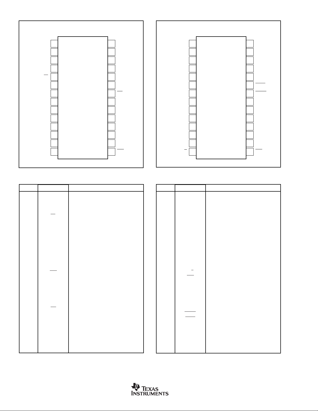
PIN CONFIGURATION: Software Mode (MODE = 0)
PIN CONFIGURATION: Hardware Mode (MODE = 1)
Top View TSSOP
NC
CDOUT
CCLK
CDIN
CS
MCLK
V
DGND
RXP
NC
SCLK
SYNC
SDATA
NC
1
2
3
4
5
6
7
IO
DIT4096
8
9
10
11
12
13
14
MODE
28
U
27
NC
26
BLS
25
NC
24
NC
23
INT
22
NC
21
NC
20
V
19
DD
TX+
18
TX–
17
DGND
16
RST
15
Top View TSSOP
CSS
COPY/C
CLK1
CLK0
MCLK
V
DGND
FMT0
FMT1
SCLK
SYNC
SDATA
M/S
1
2
L
3
4
5
6
7
IO
DIT4096
8
9
10
11
12
13
14
MODE
28
U
27
V
26
BLS
25
BLSM
24
EMPH
23
AUDIO
22
MONO
21
MDAT
20
V
19
DD
TX+
18
TX–
17
DGND
16
RST
15
PIN DESCRIPTIONS: Software Mode
PIN NAME PIN DESCRIPTION
1 NC No Connection
2 CDOUT Control Port Data Output, Tri-State
3 CCLK Control Port Data Clock Input
4 CDIN Control Port Serial Data Input
5
6 MCLK Master Clock Input
7V
8 DGND Digital Ground
9 RXP AES-3 Encoded Data Input
10 NC No Connection
11 SCLK Audio Serial Port Data Clock I/O
12 SYNC Audio Serial Port Frame SYNC Clock I/O
13 SDATA Audio Serial Port Data Input
14 NC No Connection
15
16 DGND Digital Ground
17 TX– Transmitter Line Driver Output
18 TX+ Transmitter Line Driver Output
19 V
20 NC No Connection
21 NC No Connection
22
23 NC No Connection
24 NC No Connection
25 BLS Block Start I/O
26 NC No Connection
27 U User Data Input
28 MODE Control Mode Input. Set MODE = 0 for
CS
RST
DD
INT
Control Port Chip Select Input, Active LOW
IO
Digital I/O Power Supply, +2.7V to V
Nominal
Reset Input, Active LOW
Digital Core Power Supply, +5V Nominal
Open Drain Interrupt Output, Active LOW.
Requires 10kΩ pull-up resistor to V
Software Mode operation.
PIN DESCRIPTIONS: Hardware Mode
PIN NAME PIN DESCRIPTION
1 CSS Channel Status Data Mode Input
2 COPY/C Copy Protect Input or Channel Status Se-
3 L Generation Status Input
4 CLK1 Master Clock Rate Selection Input
5 CLK0 Master Clock Rate Selection Input
DD
6 MCLK Master Clock Input
7V
IO
8 DGND Digital Ground
9 FMT0 Audio Data Format Control Input
10 FMT1 Audio Data Format Control Input
11 SCLK Audio Serial Port Data Clock I/O
12 SYNC Audio Serial Port Frame SYNC Clock I/O
13 SDATA Audio Serial Port Data Input
14
15
M/S
RST
16 DGND Digital Ground
17 TX– Transmitter Line Driver Output
18 TX+ Transmitter Line Driver Output
19 V
DD
20 MDAT Mono Mode Channel Data Selection Input
21 MONO Mono Mode Enable Input, Active HIGH
.
IO
22
23
AUDIO
EMPH
24 BLSM Block Start Mode Control Input
25 BLS Block Start I/O
26 V Validity Data Input
27 U User Data Input
28 MODE Control Mode Input. Set MODE = 1 for
rial Data Input
Digital I/O Power Supply, +2.7V to V
Nominal
Audio Serial Port Master/Slave Control Input
Reset Input, Active LOW
Digital Core Power-Supply, +5V Nominal
Audio Data Valid Control Input, Active LOW
Pre-Emphasis Status Input, Active LOW
Hardware Mode Operation.
DD
4
www.ti.com
DIT4096
SBOS225A
Page 5
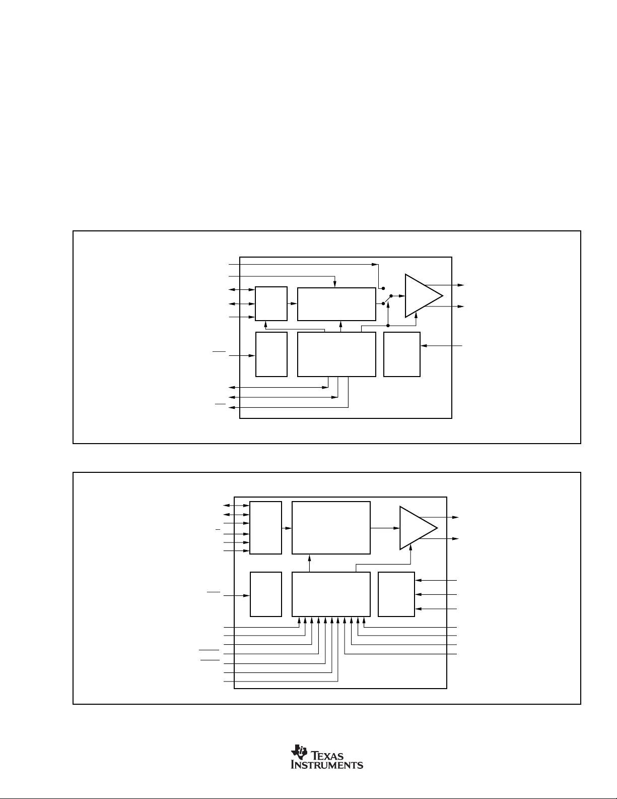
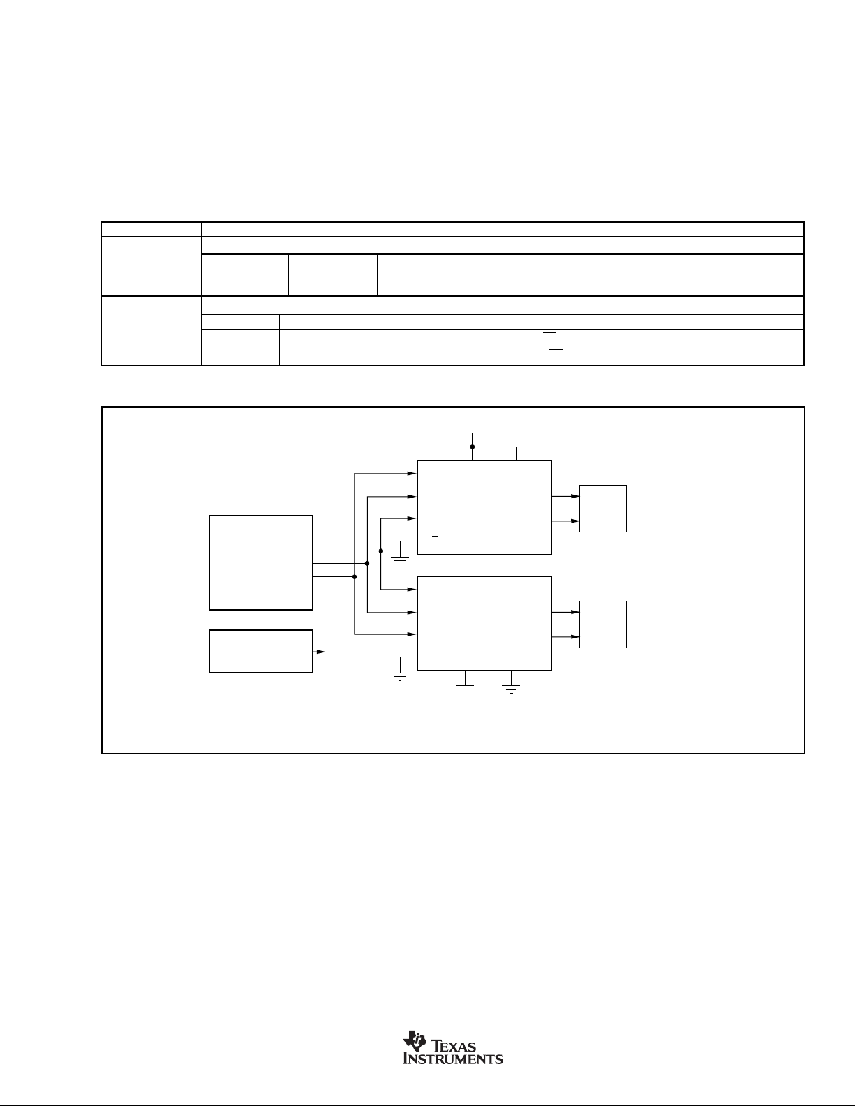
GENERAL DESCRIPTION
The DIT4096 is a complete digital audio transmitter, suitable
for both professional and consumer audio applications. Sampling rates up to 96kHz are supported. The DIT4096 complies with the requirements for the AES-3, IEC-60958, and
EIAJ CP1201 interface standards.
Figures 1 and 2 show the block diagrams for the DIT4096
when used in Software and Hardware control modes. The
MODE input (pin 28) determines the control model used to
configure the DIT4096 internal functions. In Software mode,
a serial control port is used to write and read on-chip control
registers and status buffers. In Hardware mode, dedicated
control pins are provided for configuration and status inputs.
The DIT4096 includes an audio serial port, which is used to
interface to standard digital audio sources, such as
RXP
U
SYNC
SCLK
SDATA
Audio
Serial
Port
Analog-to-Digital (A/D) converters, Digital Signal Processors
(DSPs), and audio decoders. Support for Left-Justified, RightJustified, and I
2
S data formats is provided.
The AES-3 encoder creates a multiplexed bit stream, containing audio, status, and user data. See Figure 3 for the
multiplexed data format. The data is then Bi-Phase Mark
encoded and output to a differential line driver. The line driver
outputs are connected to the transmission medium, be it
cable or fiber optics. In the case of twisted-pair or coaxial
cable, a transformer is commonly used to couple the driver
outputs to the transmission line. This provides both isolation
and improved common-mode rejection. For optical transmission, the TX+ (pin 18) driver output is connected to an optical
transmitter module. See the Applications Information section
of this data sheet for details regarding output driver circuit
configurations.
TX+
TX–
AES-3 Encoder
Line
Driver
RST
Control Port
BLS
INT
FIGURE 1. Software Mode Block Diagram.
SYNC
SCLK
SDATA
M/S
FMT0
FMT1
RST
CSS
COPY/C
L
AUDIO
EMPH
U
V
Reset
Logic
Audio
Serial
Port
Reset
Logic
Serial Control Interface,
Control Registers,
and Channel Status
Data Buffers
AES-3 Encoder
CUV
Data Buffer
Clock
Generator
Driver
Clock
Generator
Line
MCLK
TX+
TX–
MCLK
CLK0
CLK1
BLSM
BLS
MONO
MDAT
FIGURE 2. Hardware Mode Block Diagram.
DIT4096
SBOS225A
www.ti.com
5
Page 6
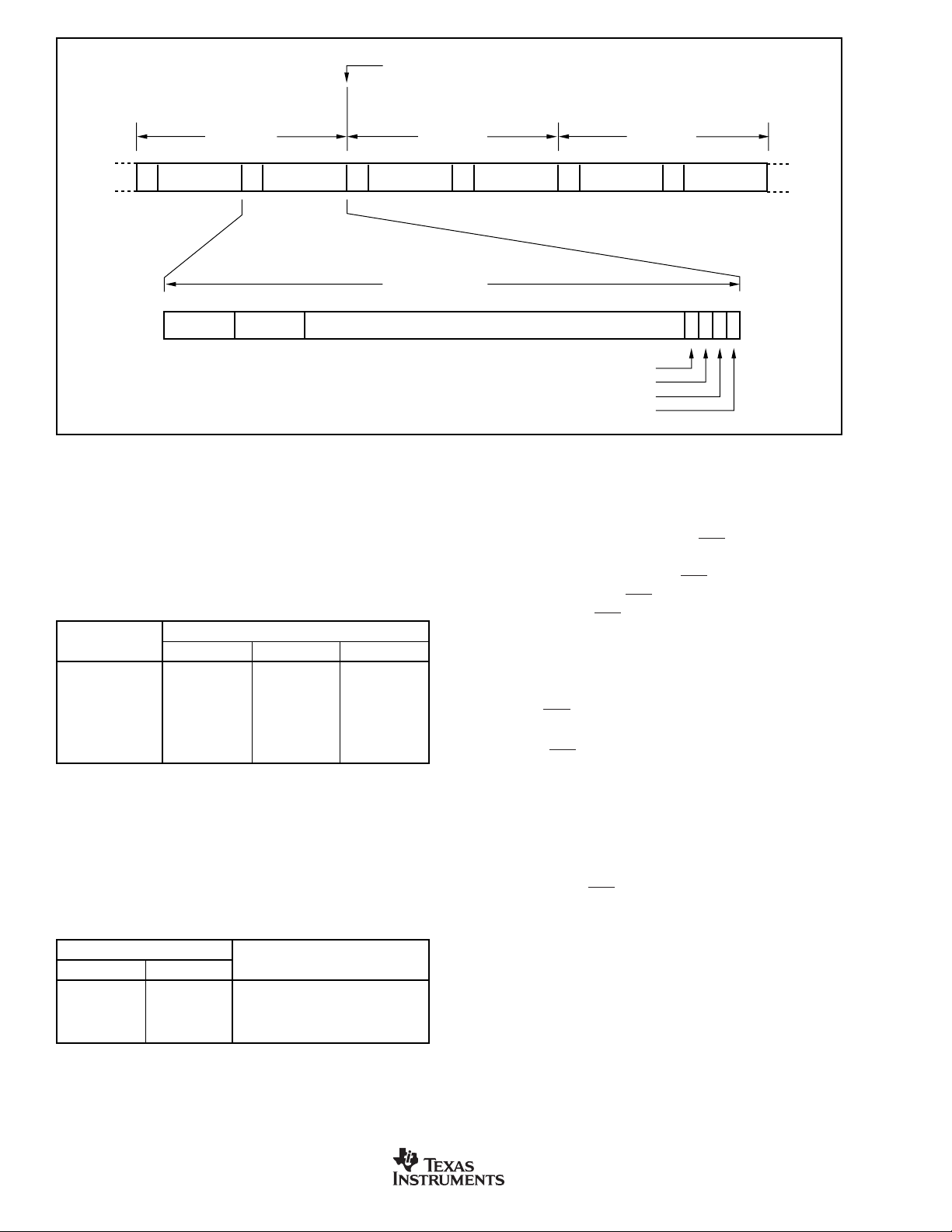
Frame 191 Frame 0 Frame 1
Channel AX XYYZ Channel A Channel A Channel BChannel BChannel B
Bits: 0 3 4 7 8
Preamble Aux Data LSB MSB V U C P
FIGURE 3. AES-3 Frame Format.
Start of Channel Status Block
One Sub-Frame
27 28 293031
Audio Data
Validity Data
User Data
Channel Status Data
Parity Bit
MASTER CLOCK
The DIT4096 requires a master clock for operation. This
clock must be supplied at the MCLK input (pin 6). The
maximum master clock frequency that may be supplied to
MCLK is 25MHz. Table I shows master clock rates for
common input sampling frequencies.
SAMPLING
FREQUENCY (kHz)
22.05 5.6448 8.4672 11.2896
24 6.144 9.216 12.288
32 8.192 12.288 16.384
44.1 11.2896 16.9344 22.5792
48 12.288 18.432 24.576
88.2 22.5792 n/a n/a
96 24.576 n/a n/a
TABLE I. Master Clock Frequencies for Common Sampling Rates.
For Software mode, the master clock frequency selection is
programmed using the CLK0 and CLK1 bits in Control
Register 02
H
CLK1 (pin 4) inputs are used to select the master clock
frequency. Table II shows the available MCLK frequency
selections.
MASTER CLOCK FREQUENCY (MHz)
256 • f
S
384 • f
S
512 • f
S
. For Hardware mode, the CLK0 (pin 5) and
RESET AND POWER-DOWN OPERATION
The DIT4096 includes a reset input,
used to force a reset sequence. When the DIT4096 is first
powered up, the user must assert
the reset sequence. The
mum of 500ns. The
RST
RST
input is then forced high to enable
normal operation. For software mode, the reset sequence will
force all internal registers to their default settings. In addition,
the reset sequence will force all channel status bits to 0 in
Software mode.
While the
RST
input is low, the transmitter outputs,
TX– (pin 17) and TX+ (pin 18), are forced to ground.
Upon setting
RST
high, the TX– and TX+ outputs will remain
low until the rising edge of the SYNC clock is detected at
pin 12. Once this occurs, the TX– and TX+ outputs will
become active and be driven by the output of the AES-3
encoder.
In Software mode, the DIT4096 also includes software reset
and power-down bits, located in control register 02
software reset bit,
RST
, and the software power-down bit,
PDN, are both active high.
RST
(pin 15), which is
RST
low, in order to start
input must be low for a mini-
. The
H
CONTROL BITS OR INPUT PINS
CLK1 CLK0
0 0 Unused
0 1 256 • f
1 0 384 • f
1 1 512 • f
MASTER CLOCK (MCLK) SELECTION
S
S
S
TABLE II. Master Clock Rate Selection for Software and
Hardware Modes.
6
www.ti.com
AUDIO SERIAL PORT
The audio serial port is a 3-wire interface used to connect the
DIT4096 to an audio source, such as an A/D converter or
DSP. The port supports sampling frequencies up to 96kHz.
The port signals include SDATA (pin 13), SYNC (pin 12), and
SCLK (pin 11). The SDATA pin is the serial data input for the
port. The SCLK pin may be either an input or output, and is
used to clock serial data into the port. The SYNC pin may be
DIT4096
SBOS225A
Page 7
either an input or output, and provides the frame synchronization clock for the port. The SYNC pin is also used as a data
latch clock for the channel status, user, and validity data
inputs in Hardware mode, and the user data input in Software
mode.
SLAVE OR MASTER MODE OPERATION
The audio serial port supports both Slave and Master mode
operation. In Slave mode, both SYNC and SCLK are configured as inputs. The audio source device must generate both
the SYNC and SCLK clocks in Slave mode. In Master mode,
both SYNC and SCLK are configured as outputs. The audio
serial port generates the SYNC and SCLK clocks in Master
mode, deriving both from the master clock (MCLK) input.
In Software mode, Master/Slave mode selection is performed using the
Slave mode). In Hardware mode, the
used to select the audio serial port mode. This is shown in
Table III.
CONTROL BITS OR INPUT PIN
TABLE III. Master/Slave Mode Selection for Software or
M/S
bit in Control Register 03H (defaults to
M/S
0
1
Hardware Mode.
M/S
input (pin 14) is
MASTER/SLAVE MODE SELECTION
Slave Mode; both SYNC and SCLK
are inputs.
Master Mode; both SYNC and SCLK
are outputs.
SYNC AND SCLK FREQUENCIES
The SYNC clock rate is the same as the sampling frequency,
or f
. This holds true for both Slave and Master modes. The
S
DIT4096 supports SYNC frequencies up to 96kHz.
The SCLK frequency in Slave mode must provide at least
one clock cycle for each data bit that is input at SDATA. The
maximum SCLK frequency is 128 • f
f
= 96kHz. The SCLK frequency in Master mode is set by
S
, or 12.288MHz for
S
the DIT4096 itself. For Software mode operation, the SCLK
rate may be programmed to either 64 • f
the SCLKR bit in Control Register 03
the SCLK frequency is fixed at 64 • f
or 128 • fS, using
S
. In Hardware mode,
H
for Master mode.
S
AUDIO DATA FORMATS
The DIT4096 supports standard audio data formats, including Philips I
Software mode provides the most flexible format selection,
while Hardware mode supports a limited subset of the
Software mode formats. Linear PCM audio data at the
SDATA input is typically presented in Binary Two’s Complement, MSB first format. Encoded or non-audio data may be
provided as required by the encoding scheme in use. Figure
4 shows the common data formats used by the audio serial
port.
2
S, Left-Justified, and Right-Justified data.
SYNC
(ISYNC = 0)
SYNC
(ISYNC = 1)
SDATA
SDATA
SDATA
SCLK
(ISCLK = 0)
SCLK
(ISCLK = 1)
SYNC
SCLK
SDATA
MSB LSB
MSB LSB
t
SYSK
t
SYSKHL
t
ADS
t
SYNCHL
t
SCLKHL
t
SCLKP
t
ADH
MSB LSB
MSB LSB
MSB LSB
Right ChannelLeft Channel
t
SYNCHL
MSB LSB
Right Justified
Left Justified
0 SCLK Delay
Left Justified
1 SCLK Delay (I
2
S)
FIGURE 4. Audio Data Formats and Timing.
DIT4096
SBOS225A
www.ti.com
7
Page 8
For Software mode, Control Register 03
EMPH
is used to set the
H
audio data format selection. Data word length may be set to
16, 18, 20, or 24 bits using the WLEN0 and WLEN1 bits.
Several format parameters, including SCLK sampling edge,
data delay from the start of frame, and SYNC polarity may be
programmed using this register. Table IV shows examples of
register bit settings for three standard audio formats. SCLK
sampling edges and SYNC polarity may differ from one
system implementation to the next. Consult the audio source
device data sheet or technical reference for details regarding
the output data formatting.
For Hardware mode, the FMT0 (pin 9) and FMT1 (pin 10)
inputs are utilized to select one of four audio data formats.
Refer to Table V for the available format selections.
falling edge of SYNC when the ISYNC bit is set to 1. If BLS
is high when it is sampled, then a block start condition is
indicated. When BLS is configured as an output and the
ISYNC bit is set to 0, BLS will go high at every 192nd falling
edge of SYNC for Stereo mode, or every 384th falling edge
of SYNC for Mono mode. BLS will then go low on the
following falling edge. If the ISYNC bit is set to 1, then BLS
transitions on the rising edge of SYNC.
Hardware mode operation is similar to Software mode operation, with the exception that there are only a limited number
of data formats available for the audio serial port. For Leftand Right-Justified formats, BLS behaves as it would in
Software mode with ISYNC = 0. For the I
2
S data format, BLS
behaves as it would in Software mode with ISYNC = 1.
INPUT PINS
FMT1 FMT0
0 0 24-Bit Left-Justified
0 1 24-Bit I
1 0 24-Bit Right-Justified
1 1 16-Bit Right-Justified
FORMAT SELECTIONS
2
S
TABLE V. Audio Data Format Selection for Hardware Mode.
AES-3 ENCODER OPERATION
The AES-3 encoder performs the multiplexing of audio,
channel status, user, and validity data. It also performs BiPhase Mark encoding of the multiplexed data stream. This
section describes how channel status, user, and validity data
are input to the encoder function.
BLOCK START INPUT/OUTPUT
The block start is used to indicate the start of a channel status
data block, which starts with Frame 0 for the AES-3 data
stream. For the DIT4096, the block start signal, BLS
(pin 25), may be either an input or output. In Software mode,
the direction of BLS is set using the BLSM bit in control register
01
(defaults to input). In Hardware mode, the direction of BLS
H
is set by the BLSM input (pin 24). If BLSM = 0, the BLS pin is
an input. If BLSM = 1, the BLS pin is an output.
For Software mode operation, the block start signal is synchronized to the audio serial port frame sync clock, SYNC
(pin 12). When BLS is configured as an input pin, it is
sampled on the rising edge of SYNC when the ISYNC bit in
control register 03
is set to 0. Otherwise, it is sampled on the
H
CHANNEL STATUS DATA INPUT
Channel status data input is determined by the control mode
in use. In Software mode, the channel status data buffer is
accessed through the serial control port. Buffer operations
are described in detail in the section of this data sheet
entitled Channel Status Buffer Operation (Software Mode
Only). In Hardware mode, channel status data input is
accomplished by one of two user-selectable methods.
THE CSS INPUT
In Hardware mode, the state of the CSS input (pin 1)
determines the function of dedicated channel status inputs.
When CSS = 0, the COPY (pin 2), L (pin 3),
and
(pin 23) inputs are used to set associated
channel status data bits. The COPY and L inputs are used to
setup copy protection for consumer operation, or indicate
that the transmitter is operating in professional mode, without
copy protection. The
AUDIO
input is utilized to indicate
whether the data being transmitted is PCM audio data, or
non-audio data. The EMPH
input is used to indicate whether
the PCM audio data has been pre-emphasized using the
50/15µs standard. See Table VI for the available options for
these dedicated channel status inputs.
When CSS = 1, the channel status data is input in a serial
fashion at the C input (pin 2). Data is clocked on the rising
and falling edges of the SYNC input (pin 12). All channel
status data bits can be written in this mode, allowing greater
flexibility than the previous Hardware mode case with
CSS = 0. See Figure 5 for the C input timing diagram.
AUDIO
(pin 22),
CONTROL REGISTER 03
AUDIO DATA
FORMATS
2
Phillips I
S 0 Left-Justified 1 1 SCLK Delay 0 Rising Edge 1 Inverted
Left-Justified 0 Left-Justified 0 0 SCLK Delay 0 Rising Edge 0 Noninverted
Right-Justified 1 Right-Justified 0 0 SCLK Delay 0 Rising Edge 0 Noninverted
Bit Name Function Bit Name Function Bit Name Function Bit Name Function
JUS Justification DELAY SCLK Delay ISCLK Sampling Edge ISYNC Phase
BIT SETTINGS
H
TABLE IV. Audio Data Format Selection in Software Mode.
8
www.ti.com
DIT4096
SBOS225A
Page 9

INPUT FUNCTION
COPY Copy Status
L Generation Status
COPY L Status
0 0 Consumer Mode, PRO = 0, COPY = 0, L = 0
0 1 Consumer Mode, PRO = 0, COPY = 0, L = 1
1 0 Consumer Mode, PRO = 0, COPY = 1, L = 0
1 1 Professional Mode, PRO = 1, No Copy Protection
AUDIO Audio Data Status
AUDIO Status
0 Digital (or Linear PCM) Audio Data.
1 Non-Audio or Encoded Audio Data.
EMPH Pre-Emphasis Status
EMPH Status
0 Pre-emphasis bits are set to indicate 50/15µs Pre-emphasis has been applied.
1 Pre-emphasis bits are set to indicate that no Pre-emphasis has been applied.
TABLE VI. Channel Status Data Input for Hardware Mode with CSS = 0.
Block Start
Frame 191 or 383 Frame 0
(1)
SYNC
BLS
(Input)
BLS
(Output)
C, U, or V
Data
192nd or 384th
Falling Edge
Ch B
Data
NOTE: (1) Assumes ISYNC = 0.
t
CUVS
(1)
Ch A
Data
FIGURE 5. C, U, and V Data Timing.
USER AND VALIDITY DATA INPUT
The user data bits in the AES-3 data stream allow for a
convenient way to transfer user-defined or application specific data to another device containing an AES-3 receiver.
The U input (pin 27) is used in both Software and Hardware
mode to input the user data in a serial fashion. Figure 5
shows the U input timing diagram.
Validity data is used to indicate that a sample is error-free
audio data, or that the sample is defective and is not suitable
t
CUVH
Ch B
Data
Ch A
Data
for further processing. In Software mode, the VAL bit in
control register 01
is utilized to write the validity data. In
H
Hardware mode, the V input (pin 26) is used to input the
validity data in serial fashion. Refer to Figure 5 for V input
timing for Hardware Mode.
When VAL or V = 0, this indicates that the audio data is valid
and suitable for further processing. When VAL or V = 1, then
the audio sample is defective and should not be used.
DIT4096
SBOS225A
www.ti.com
9
Page 10

LINE DRIVER OUTPUTS
The DIT4096 includes a balanced line driver. The line driver
outputs are TX– (pin 17) and TX+ (pin 18). In Software mode,
the line driver input is taken from either the output of the onchip AES-3 encoder, or from an external AES-3 encoded
source input at RXP (pin 9). The input source is selected
using the BYPASS bit in control register 01
(defaults to the
H
on-chip AES-3 encoder). In Hardware mode, the line driver
source is always the on-chip AES-3 encoder.
The outputs of the line driver will follow the AES-3 encoded
data source in normal operation. During a hardware or
software reset, or when the device is in power-down mode,
the line driver outputs will be forced to ground. The outputs
can also be forced to ground at any time in Software mode
by setting the TXOFF bit to 1 in control register 01
.
H
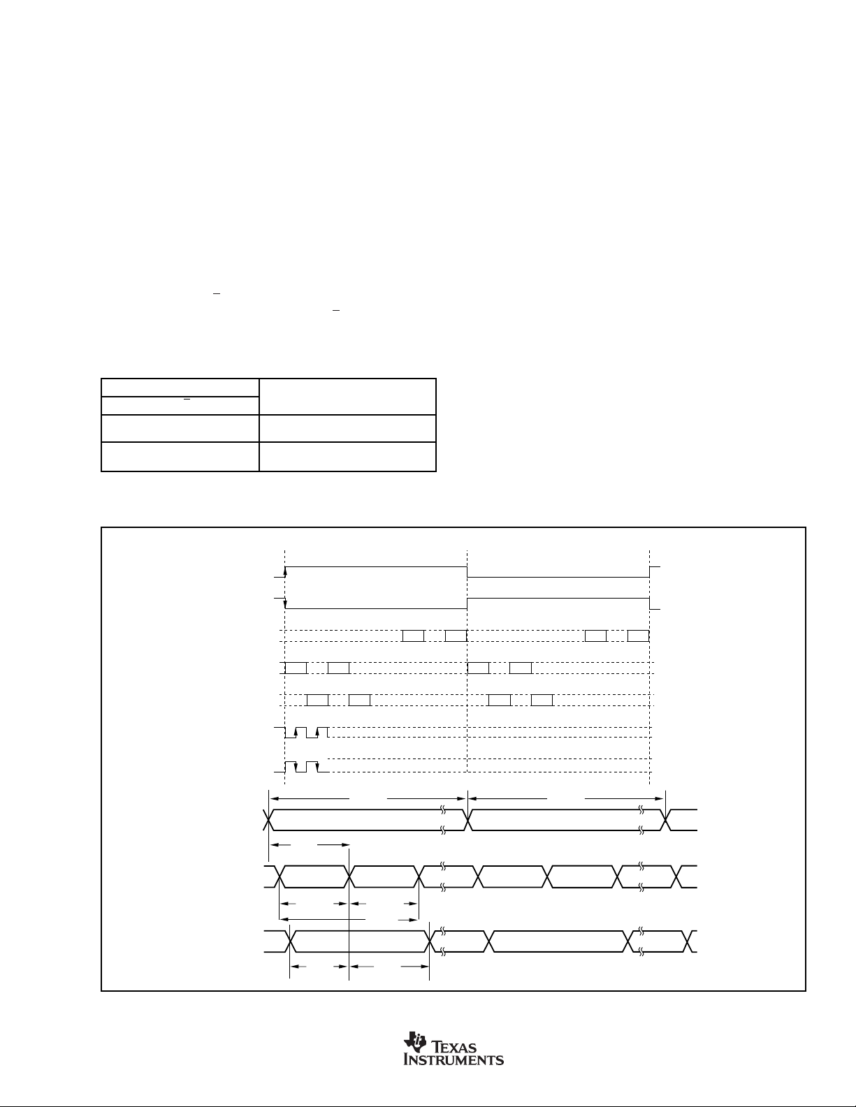
CONTROL PORT OPERATION (SOFTWARE MODE ONLY)
For Software mode operation, the DIT4096 includes a serial
control port, which is used to write and read control registers
and the channel status data buffer. Port signals include
(pin 5), CDIN (pin 4), CDOUT (pin 2), and CCLK (pin 3).
CS
is the active low chip select. This signal must be driven
low in order to write or read control registers and the channel
status data buffer.
CDIN is the serial data input, while CDOUT serves as the
serial data output. The CDOUT pin is a tri-state output, which
is set to a high-impedance state when not performing a Read
operation, or when
CS
= 1.
CS
CCLK is the data clock for the serial control interface. Data
is clocked in at CDIN on the rising edge of CCLK, while data
is clocked out at CDOUT on the falling edge of CCLK. Data
is clocked MSB first for both CDIN and CDOUT.
WRITE OPERATION
Figure 6 illustrates the write operation for the control port.
You may write one register or buffer address at a time, or use
the auto-increment capability built into the control port to
perform block writes. The register or buffer data is preceded
by a 16-bit header, with the first byte being used to configure
control port operation and set the starting register or buffer
address. The second byte of the header is comprised of
“don’t care” bits, which can be set to either 0 or 1 without
affecting port operation.
The first byte of the header contains two control bits, R/W
and STEP, followed by a 6-bit address. For write operations,
R/W
= 0. The STEP bit determines the address step size for
the auto-increment operation. When STEP = 0, the address
is incremented by 1. When STEP = 1, the address is
incremented by 2. Incrementing by 1 is useful when writing
multiple control registers in sequence, or when writing both left
and right channel status data in sequence. Incrementing by 2
is useful when writing just one channel of status data in
sequence.
The third byte contains the 8-bit data for the register or buffer
address designated by the first byte of the header. To write a
single address location,
significant bit of the third byte is clocked into the port. For auto
increment mode,
CS
or buffer addresses.
CS
is brought high after the least
is kept low to write successive register
Set CS = 1 here to write one register or buffer location.
CS
Header
CDIN
CCLK
BYTE DEFINITION
BYTE 0:
Byte 1: All 8 bits are Don’t Care. Set 0 or 1.
Bytes 2 through N: 8-Bit Register or Buffer data.
Byte 0 Byte 1 Byte 2 Byte 3 Byte N
MSB LSB
R/WSTEPA5A4A3A2A1A0
Register or Buffer Address
Auto-Increment Address Step Size: 0 = Increment Address by 1
Read/Write Control: Set to 1 for Read Operation
FIGURE 6. Write Operation Format.
Keep CS = 0 to enable auto-increment mode.
Register or Buffer Data
1 = Increment Address by 2
10
www.ti.com
DIT4096
SBOS225A
Page 11

READ OPERATION
Figure 7 shows an illustration of the read operation for the
control port. You may read one register or buffer address at
a time, or use the auto-increment capability built into the
control port to perform block reads. A 16-bit header is first
written to the port, with the first byte being used to configure
control port operation and set the starting register or buffer
address. The second byte of the header is comprised of
“don’t care” bits, which can be set to either 0 or 1 without
affecting port operation.
The first byte of the header contains two control bits, R/W
and STEP, followed by a 6-bit address. For read operations,
R/W
= 1. The STEP bit determines the address step size for
the auto-increment operation. When STEP = 0, the address
is incremented by 1. When STEP = 1, the address is
incremented by 2. Incrementing by 1 is useful when reading
multiple control registers in sequence, or when reading both
left and right channel status data in sequence. Incrementing
by 2 is useful for reading just one channel of status data in
sequence.
The first output data byte occurs immediately after the 16-bit
header has been written. This byte contains the 8-bit data for
the register or buffer address pointed to by the first byte of
the header. To read a single address location,
CS
is brought
high after the least significant bit of the first data byte is
clocked out of the port. For auto increment mode,
CS
is kept
low to read successive register or buffer addresses.
Set CS = 1 here to read one register or buffer location.
CS
CDIN
CDOUT
CCLK
BYTE DEFINITION
BYTE 0:
Byte 0 Byte 1
High Impedance
MSB LSB
R/WSTEPA5A4A3A2A1A0
Byte 1: All 8 bits are Don’t Care. Set 0 or 1.
Bytes 2 through N: 8-Bit Register or Buffer data.
FIGURE 7. Read Operation Format.
Keep CS = 0 to enable auto-increment mode.
Header
Ignore Until Next High-to-Low Transition of CS
Register or Buffer Data
Byte 0 Byte 1
Register or Buffer Address
Auto-Increment Address Step Size: 0 = Increment Address by 1
Read/Write Control: Set to 1 for Read Operation
1 = Increment Address by 2
Byte N
CS
CCLK
CDIN
CDOUT
FIGURE 8. Serial Port Timing.
DIT4096
SBOS225A
t
CSCR
t
SDS
t
t
CFDO
www.ti.com
SDH
t
CFCS
t
CSZ
11
Page 12

CONTROL REGISTER DEFINITIONS (SOFTWARE MODE ONLY)
This section defines the control registers used to configure
the DIT4096, as well as the status register used to indicate
an interrupt source.
Register 00H: Reserved for Factory Use
Bit 7 (MSB) Bit 6 Bit 5 Bit 4 Bit 3 Bit 2 Bit 1 Bit 0 (LSB)
00000000
BLSM Block Start Mode (Defaults to 0)
When set to 0, BLS (pin 25) is configured as an
input pin.
When set to 1, BLS (pin 25) is configured as an
output pin.
VAL Audio Data Valid (Defaults to 0)
When set to 0, valid Linear PCM audio data is
indicated.
When set to 1, invalid audio data or non-PCM
data is indicated.
When MONO = 1 and MCSD = 0, the MDAT bit
is used to select the source for Audio data.
When MONO = 1 and MCSD = 1, the MDAT bit
is used to select the source for both Audio and
Channel Status data.
MCSD Channel Status Data Selection (Defaults to 0)
When set to 0, Channel A data is used for the A
sub-frame, while Channel B data is used for the
B sub-frame.
When set to 1, use the same channel status data
for both A and B sub-frames. Channel status
data source is selected using the MDAT bit.
TXOFF Transmitter Output Disable (Defaults to 0)
When set to 0, the line driver outputs, TX–
(pin 17) and TX+ (pin 18) are enabled.
When set to 1, the line driver outputs are
forced to ground.
Register 02H: Power-Down and Clock Control Register
Bit 7 (MSB) Bit 6 Bit 5 Bit 4 Bit 3 Bit 2 Bit 1 Bit 0 (LSB)
0 0 0 0 RST CLK1 CLK0 PDN
Register 01H: Transmitter Control Register
Bit 7 (MSB) Bit 6 Bit 5 Bit 4 Bit 3 Bit 2 Bit 1 Bit 0 (LSB)
TXOFF MCSD MDAT MONO BYPAS MUTE VAL BLSM
MUTE Transmitter Mute (Defaults to 0)
When set to 0, the mute function is disabled.
When set to 1, the mute function is enabled,
with Channel A and B audio data set to all 0’s.
BYPASS Transmitter Bypass—AES-3 Data Source for
the Output Driver (Defaults to 0)
When set to 0, AES-3 encoded data is taken
from the output of the on-chip encoder.
When set to 1, RXP (pin 9) is used as the
source for AES-3 encoded data.
MONO Mono Mode Control (Defaults to 0)
When set to 0, the transmitter is set to Stereo
mode.
When set to 1, the transmitter is set to Mono
mode.
MDAT Data Selection Bit (Defaults to 0)
(0 = Left Channel, 1 = Right Channel)
When MONO = 0 and MCSD = 0, the MDAT bit
is ignored.
When MONO = 0 and MCSD = 1, the MDAT bit
is used to select the source for Channel
Status data.
PDN Power-Down (Defaults to 1)
When set to 0, the DIT4096 operates normally.
When set to 1, the DIT4096 is powered down,
with the line driver outputs forced to ground.
CLK[1:0] MCLK Rate Selection
These bits are used to select the master clock
frequency applied to the MCLK input (pin 6).
CLK1 CLK0 MCLK Rate
0 0 Unused
0 1 256 • f
1 0 384 • f
1 1 512 • f
(default)
S
S
S
RST Software Reset (Defaults to 0)
When set to 0, the DIT4096 operates normally.
When set to 1, the DIT4096 is reset.
Register 03H: Audio Serial Port Control Register
Bit 7 (MSB) Bit 6 Bit 5 Bit 4 Bit 3 Bit 2 Bit 1 Bit 0 (LSB)
ISYNC ISCLK DELAY JUS WLEN1 WLEN0 SCLKR M/S
M/S Master/Slave Mode (Defaults to 0)
When set to 0, the audio serial port is set for
Slave operation.
When set to 1, the audio serial port is set for
Master operation.
12
www.ti.com
DIT4096
SBOS225A
Page 13

SCLKR Master Mode SCLK Frequency (Defaults to 0)
When set to 0, the SCLK frequency is set to
64 • f
.
S
When set to 1, the SCLK frequency is set to
128 • f
.
S
WLEN[1:0] Audio Data Word Length
These bits are used to set the audio data word
length for both Left and Right channels.
BTI Buffer Transfer Interrupt Status—Active
High
When User Access (UA) to Transmitter Access
(TA) buffer transfers are enabled, and the BTI
interrupt is unmasked, this bit will go HIGH
when a UA to TA buffer transfer has completed. This will also cause the INT
output
(pin 22) to be driven LOW, indicating that an
interrupt has occurred.
WLEN1 WLEN0 Length
0 0 24 Bits (default)
0 1 20 Bits
1 0 18 Bits
1 1 16 Bits
JUS Audio Data Justification (Defaults to 0)
When set to 0, the audio data is Left-Justified
with respect to the SYNC edges.
When set to 1, the audio data is Right-Justified
with respect to the SYNC edges.
DELAY Audio Data Delay from the Start of Frame
(Defaults to 0)
This applies primarily to I
2
S and DSP frame
formats, which use Left-Justified audio data.
When set to 0, audio data starts with the SCLK
period immediately following the SYNC edge
which starts the frame. This is referred to as a
zero SCLK delay.
When set to 1, the audio data starts with the
second SCLK period following the SYNC edge
which starts the frame. This is referred to as a
one SCLK delay. This is used primarily for the
2
I
S data format.
ISCLK SCLK Sampling Edge (Defaults to 0)
When set to 0, audio serial data at SDATA
(pin 13) is sampled on rising edge of SCLK.
When set to 1, audio serial data at SDATA
(pin 13) is sampled on falling edge of SCLK.
TSLIP Transmitter Source Data Slip Interrupt Sta-
tus—Active High
This bit will go HIGH when either a Data Slip or
Block Start condition is detected, and the TSLIP
interrupt is unmasked. This will also cause the
INT
output (pin 22) to be driven LOW, indicating that an interrupt has occurred. The function
of this bit is selected using the BSSL bit in
control register 05
(defaults Data Slip).
H
The MBTI and MTSLIP bits are used to mask
the BTI and TSLIP interrupts. When masked,
these interrupt sources are disabled.
Register 05H: Interrupt Mask Register
Bit 7 (MSB) Bit 6 Bit 5 Bit 4 Bit 3 Bit 2 Bit 1 Bit 0 (LSB)
0 0 0 0 0 BSSL MTSLIP MBTI
MBTI BTI Interrupt Mask. Set to ‘0’ to mask BTI
(Defaults to 0).
MTSLIP TSLIP Interrupt Mask. Set to ‘0’ to mask
TSLIP (Defaults to 0).
BSSL TSLIP Interrupt Select (Defaults to 0)
When set to 0, the Data Slip condition is used
to trigger a TSLIP interrupt.
When set to 1, the Block Start condition is
used to trigger a TSLIP interrupt.
Register 06H: Interrupt Mode Register
Bit 7 (MSB) Bit 6 Bit 5 Bit 4 Bit 3 Bit 2 Bit 1 Bit 0 (LSB)
0 0 0 0 TSLIPM1 TSLIPM0 BTIM1 BTIM0
ISYNC SYNC Polarity (Defaults to 0)
When set to 0, Left channel data occurs when
the SYNC clock is HIGH.
When set to 1, Left channel data occurs when
the SYNC clock is LOW.
For both cases, Left channel data always precedes the Right channel data in the audio frame.
Register 04H: Interrupt Status Register
Bit 7 (MSB) Bit 6 Bit 5 Bit 4 Bit 3 Bit 2 Bit 1 Bit 0 (LSB)
0 0 0 0 0 0 TSLIP BTI
DIT4096
SBOS225A
www.ti.com
BTIM[1:0] BTI Interrupt Mode
TSLIPM[1:0] TSLIP Interrupt Mode
These bits are used to select the active state
for interrupt operation.
BTIM1 or BTIM0 or
TSLIPM1 TSLIPM0 Interrupt Operation
0 0 Rising Edge Active (default)
0 1 Falling Edge Active
1 0 Level Active
1 1 Reserved
13
Page 14

BTD Buffer Transfer Disable (Defaults to 0)
When set to 0, User Access (UA) to Transmitter Access (TA) Buffer transfers are enabled.
When set to 1, User Access (UA) to Transmitter Access (TA) Buffer transfers are disabled.
Register 07H: Channel Status Buffer Control Register
bit 7 (MSB) bit 6 bit 5 bit 4 bit 3 bit 2 bit 1 bit 0 (LSB)
0000000BTD
CHANNEL STATUS DATA BUFFER OPERATION (SOFTWARE MODE ONLY)
The DIT4096 contains two buffers for the channel status data.
These are referred to as the Transmitter Access (TA) buffer
and the User Access (UA) buffer. Each buffer is 48 bytes long,
containing 24 bytes each for channels A and B. The 24 bytes
per channel correspond to the channel status block defined in
the AES-3 and IEC-60958 specifications. Channel A and B
data are interleaved within the buffers, see Tables VII and VIII.
The AES-3 encoder internally accesses the TA buffer to
obtain the channel status data that is multiplexed into the
AES-3 data stream. The user accesses the UA buffer through
the control port in order to update the channel status data
when needed. The transfer of data from the UA buffer to the
TA buffer is managed internally by the DIT4096, but it may
be enabled or disabled by the user via a control register.
The master clock input (MCLK) and the frame synchronization clock input (SYNC) muct be active in order to update the
channel status buffer in Software mode. When the DIT4096
is initially powered up, the device defaults to power-down
mode. When the PDN bit in Register 2 is set to 0 to power
up the device, there must be a delay between the time that
PDN is set to 0 and the first access to the channel status
buffer. This delay allows the SYNC clock to synchronize the
AES3 encoder block with the audio serial port. It is recommended that Register 2 be the last register written in the
initialization sequence, followed by a delay (10 milliseconds
or longer) before attempting to access the channel status
buffer.
UPDATING THE CHANNEL DATA STATUS BUFFER
Updating the channel status data buffer involves disabling
and enabling the UA to TA buffer transfer using the BTD bit
in control register 07
updating the buffer.
The BTD bit is normally set to 0, which enables the UA to TA
buffer transfer. In order to update the channel status data,
the user must write to the UA buffer. To avoid UA to TA data
transfer while the UA buffer is being updated, the BTD bit is
set to 1, which disables UA to TA buffer transfers. While
BTD = 1, the user writes new channel status data to the UA
buffer via the control port. Once the UA buffer update is
complete, the BTD bit is reset to 0. A new UA to TA buffer
transfer will occur during one of the frames 184 through 191,
. Figure 9 shows the proper flow for
H
NO
Read Register 04H to verify that the
The Host has verified that the Buffer
Transfer is complete, which completes the
Channel Status Data update.
Is the
INT output LOW?
YES
BTI bit is set to 1.
DISABLE UA TO TA BUFFER TRANSFER
ENABLE UA TO TA BUFFER TRANSFER
NO
Set BTD = 1
in Control Register 07
UPDATE THE CS DATA
Write Channel Status Data
to the UA Buffer
Set BTD = 0
in Control Register 07
Is the
Buffer Transfer Interrupt (BTI)
Masked?
H
H
YES
Assume that the Buffer Transfer has
completed and that the Channel Status
data has been updated.
FIGURE 9. Flowchart for Updating the Channel Status Buffer.
14
www.ti.com
DIT4096
SBOS225A
Page 15

ADDRESS CS BIT 0 BIT 1 BIT 2 BIT 3 BIT 4 BIT 5 BIT 6 BIT 7
(HEX) Byte MSB LSB
08 A0 PRO AUDIO EMPH EMPH EMPH LOCK f
09 B0 PRO AUDIO EMPH EMPH EMPH LOCK f
0A A1
0B B1
0C A2 AUX AUX AUX WLEN WLEN WLEN reserved reserved
0D B2 AUX AUX AUX WLEN WLEN WLEN reserved reserved
0E A3 reserved reserved reserved reserved reserved reserved reserved reserved
0F B3 reserved reserved reserved reserved reserved reserved reserved reserved
10 A4 REF REF reserved reserved reserved reserved reserved reserved
11 B4 REF REF reserved reserved reserved reserved reserved reserved
12 A5 reserved reserved reserved reserved reserved reserved reserved reserved
13 B5 reserved reserved reserved reserved reserved reserved reserved reserved
14 A6 Alphanumeric Channel Origin Data (7-Bit ASCII0) for Channel A
15 B6 Alphanumeric Channel Origin Data (7-Bit ASCII0) for Channel B
16 A7 Alphanumeric Channel Origin Data (7-Bit ASCII0) for Channel A
17 B7 Alphanumeric Channel Origin Data (7-Bit ASCII0) for Channel B
18 A8 Alphanumeric Channel Origin Data (7-Bit ASCII0) for Channel A
19 B8 Alphanumeric Channel Origin Data (7-Bit ASCII0) for Channel B
1A A9 Alphanumeric Channel Origin Data (7-Bit ASCII0) for Channel A
1B B9 Alphanumeric Channel Origin Data (7-Bit ASCII0) for Channel B
1C A10 Alphanumeric Channel Destination Data (7-Bit ASCII) for Channel A
1D B10 Alphanumeric Channel Destination Data (7-Bit ASCII) for Channel B
1E A11 Alphanumeric Channel Destination Data (7-Bit ASCII) for Channel A
1F B11 Alphanumeric Channel Destination Data (7-Bit ASCII) for Channel B
20 A12 Alphanumeric Channel Destination Data (7-Bit ASCII) for Channel A
21 B12 Alphanumeric Channel Destination Data (7-Bit ASCII) for Channel B
22 A13 Alphanumeric Channel Destination Data (7-Bit ASCII) for Channel A
23 B13 Alphanumeric Channel Destination Data (7-Bit ASCII) for Channel B
24 A14 Local Sample Address Code (32-Bit Binary) for Channel A
25 B14 Local Sample Address Code (32-Bit Binary) for Channel B
26 A15 Local Sample Address Code (32-Bit Binary) for Channel A
27 B15 Local Sample Address Code (32-Bit Binary) for Channel B
28 A16 Local Sample Address Code (32-Bit Binary) for Channel A
29 B16 Local Sample Address Code (32-Bit Binary) for Channel B
2A A17 Local Sample Address Code (32-Bit Binary) for Channel A
2B B17 Local Sample Address Code (32-Bit Binary) for Channel B
2C A18 Time of Day Code (32-Bit Binary) for Channel A
2D B18 Time of Day Code (32-Bit Binary) for Channel B
2E A19 Time of Day Code (32-Bit Binary) for Channel A
2F B19 Time of Day Code (32-Bit Binary) for Channel B
30 A20 Time of Day Code (32-Bit Binary) for Channel A
31 B20 Time of Day Code (32-Bit Binary) for Channel B
32 A21 Time of Day Code (32-Bit Binary) for Channel A
33 B21 Time of Day Code (32-Bit Binary) for Channel B
34 A22 reserved reserved reserved reserved Rel Flags Rel Flags Rel Flags Rel Flags
35 B22 reserved reserved reserved reserved Rel Flags Rel Flags Rel Flags Rel Flags
36 A23 CRC Check Character for Channel A
37 B23 CRC Check Character for Channel B
CH MODE CH MODE CH MODE CH MODE U BIT MGT U BIT MGT U BIT MGT U BIT MGT
CH MODE CH MODE CH MODE CH MODE U BIT MGT U BIT MGT U BIT MGT U BIT MGT
S
S
f
S
f
S
TABLE VII. Channel Status Buffer Map for Professional Mode (PRO = 1).
DIT4096
SBOS225A
www.ti.com
15
Page 16

ADDRESS CS BIT 0 BIT 1 BIT 2 BIT 3 BIT 4 BIT 5 BIT 6 BIT 7
(HEX) Byte MSB LSB
8 A0 PRO = 0 AUDIO COPY EMPH EMPH EMPH MODE MODE
09 B0 PRO = 0 AUDIO COPY EMPH EMPH EMPH MODE MODE
0A A1
0B B1
0C A2 SOURCE SOURCE SOURCE SOURCE CH NUM CH NUM CH NUM CH NUM
0D B2 SOURCE SOURCE SOURCE SOURCE CH NUM CH NUM CH NUM CH NUM
0E A3 f
0F B3 f
10 A4 reserved reserved reserved reserved reserved reserved reserved reserved
11 B4 reserved reserved reserved reserved reserved reserved reserved reserved
12 A5 reserved reserved reserved reserved reserved reserved reserved reserved
13 B5 reserved reserved reserved reserved reserved reserved reserved reserved
14 A6 reserved reserved reserved reserved reserved reserved reserved reserved
15 B6 reserved reserved reserved reserved reserved reserved reserved reserved
16 A7 reserved reserved reserved reserved reserved reserved reserved reserved
17 B7 reserved reserved reserved reserved reserved reserved reserved reserved
18 A8 reserved reserved reserved reserved reserved reserved reserved reserved
19 B8 reserved reserved reserved reserved reserved reserved reserved reserved
1A A9 reserved reserved reserved reserved reserved reserved reserved reserved
1B B9 reserved reserved reserved reserved reserved reserved reserved reserved
1C A10 reserved reserved reserved reserved reserved reserved reserved reserved
1D B10 reserved reserved reserved reserved reserved reserved reserved reserved
1E A11 reserved reserved reserved reserved reserved reserved reserved reserved
1F B11 reserved reserved reserved reserved reserved reserved reserved reserved
20 A12 reserved reserved reserved reserved reserved reserved reserved reserved
21 B12 reserved reserved reserved reserved reserved reserved reserved reserved
22 A13 reserved reserved reserved reserved reserved reserved reserved reserved
23 B13 reserved reserved reserved reserved reserved reserved reserved reserved
24 A14 reserved reserved reserved reserved reserved reserved reserved reserved
25 B14 reserved reserved reserved reserved reserved reserved reserved reserved
26 A15 reserved reserved reserved reserved reserved reserved reserved reserved
27 B15 reserved reserved reserved reserved reserved reserved reserved reserved
28 A16 reserved reserved reserved reserved reserved reserved reserved reserved
29 B16 reserved reserved reserved reserved reserved reserved reserved reserved
2A A17 reserved reserved reserved reserved reserved reserved reserved reserved
2B B17 reserved reserved reserved reserved reserved reserved reserved reserved
2C A18 reserved reserved reserved reserved reserved reserved reserved reserved
2D B18 reserved reserved reserved reserved reserved reserved reserved reserved
2E A19 reserved reserved reserved reserved reserved reserved reserved reserved
2F B19 reserved reserved reserved reserved reserved reserved reserved reserved
30 A20 reserved reserved reserved reserved reserved reserved reserved reserved
31 B20 reserved reserved reserved reserved reserved reserved reserved reserved
32 A21 reserved reserved reserved reserved reserved reserved reserved reserved
33 B21 reserved reserved reserved reserved reserved reserved reserved reserved
34 A22 reserved reserved reserved reserved reserved reserved reserved reserved
35 B22 reserved reserved reserved reserved reserved reserved reserved reserved
36 A23 reserved reserved reserved reserved reserved reserved reserved reserved
37 B23 reserved reserved reserved reserved reserved reserved reserved reserved
CAT CODE CAT CODE CAT CODE CAT CODE CAT CODE CAT CODE CAT CODE
CAT CODE CAT CODE CAT CODE CAT CODE CAT CODE CAT CODE CAT CODE
S
S
f
S
f
S
f
S
f
S
f
S
f
S
CLK ACC CLK ACC reserved reserved
CLK ACC CLK ACC reserved reserved
TABLE VIII. Channel Status Buffer for Consumer Mode (PRO = 0).
L
L
whichever is the first frame to occur after the BTD bit is reset
to 0. Once the UA to TA buffer transfer is completed, the buffer
transfer interrupt (BTI) will occur, as long as it is unmasked.
The transmitter will ignore any attempt to access the UA
buffer during a UA to TA buffer transfer. In addition, the BTD
bit may be set to 1 to stop a UA to TA buffer transfer that may
be in progress, if so desired.
CHANNEL STATUS BUFFER MAP
The channel status buffer is organized in accordance with the
AES-3 and IEC-60958 standards. See Table VII for the memory
map for the UA channel status data buffer for Professional mode.
Table VIII shows the memory map for the UA channel status data
buffer for Consumer mode.
16
www.ti.com
INTERRUPT SOURCES (SOFTWARE MODE ONLY)
The DIT4096 can be programmed to generate interrupts for
up to three predefined conditions. The interrupt output, INT
(pin 22), is set low when a valid interrupt occurs. The interrupt
status register, 04
the interrupt. Status register bits and the INT
remain active until the status register is read. Once read,
status bits are cleared and the INT
external pull-up resistor to V
Interrupts may be masked using control register 05H. When
masked, the interrupt mechanism associated with a particular
status bit is disabled.
, is then read to determine the source of
H
output pin
pin is pulled high by an
.
IO
DIT4096
SBOS225A
Page 17

CHANNEL STATUS BUFFER TRANSFER INTERRUPT
This interrupt occurs when a channel status buffer transfer
has been completed. This interrupt may be used by the host
to trigger an event to occur after a channel status buffer
update. The BTI bit in status register 04
the occurrence of the buffer transfer. The BTI bit, like all other
status bits, is active high and remains set until the status
register is read.
is used to indicate
H
A block start condition occurs when a block start signal is
generated either internally by the DIT4096, or when an
external block start is received at the BLS input (pin 25).
APPLICATIONS INFORMATION
This section provides practical information pertinent for
designing the DIT4096 into a target application. Circuit
schematics are provided as needed.
DATA SLIP AND BLOCK START INTERRUPTS
Unlike the BTI interrupt, which has only one function, the TSLIP
interrupt can be set to one of two modes. This is accomplished
using the BSSL bit in control register 05
TSLIP interrupt is set to indicate a data slip condition. When
BSSL = 1, the TSLIP interrupt is set to indicate a block start
condition. The TSLIP bit, like all other status bits, is active high
and remains set until the status register is read.
A data slip condition may occur in cases where the master clock,
MCLK (pin 6), is asynchronous to the audio data source. When
BSSL = 0, the TSLIP bit will be set to 1 every time a data sample
is dropped or repeated.
Digital Audio
Source
(A/D Converter,
µP or DSP
Audio Master
. When BSSL = 0, the
H
From AES-3
Encoded Data
Source
(Optional)
DSP)
Clock
DIT4096
9
RXP
11
SCLK
12
SYNC
13
SDATA
5
CS
3
CCLK
4
CDIN
2
CDOUT
22
INT
25
BLS
27
U
15
RST
6
MCLK
28
MODE
TYPICAL APPLICATION DIAGRAMS
Figures 10 and 11 illustrate the typical application schematics for the DIT4096 when used in Software and Hardware
modes. Figure 10 shows a typical Software mode application, where a microprocessor or DSP interface is used to
communicate with the DIT4096 via the serial control port.
See Figure 11 for a typical Hardware mode configuration,
where the control pins are either hardwired or driven by
digital logic in a stand-alone application.
The recommended component values for power-supply
bypass capacitors are shown in Figures 10 and 11. These
capacitors should be located as close to the DIT4096
power-supply pins as physically possible.
18
TX+
Cable or
Fiber Optics
= C2 = 0.1µF to 1µF
C
1
TX–
V
DGND
V
DGND
IO
DD
17
+2.7V to V
7
8
19
16
Output
Circuit
(See Figs. 12-14)
DD
C
1
+5V
C
2
10kΩ
V
IO
FIGURE 10. Typical Circuit Configuration, Software Mode.
DIT4096
SBOS225A
www.ti.com
17
Page 18

Digital Audio
Source
(A/D Converter,
DSP)
Hardwired
Control
or
Dedicated
Logic
or
Host
Controlled
Audio Master
Clock Generator
DIT4096
11
SCLK
12
SYNC
13
SDATA
14
M/S
9
FMT0
10
FMT1
1
CSS
2
COPY/C
27
U
26
V
3
L
22
AUDIO
23
EMPH
24
BLSM
21
MONO
20
MDAT
15
RST
25
BLS
6
MCLK
5
CLK0
4
CLK1
28
MODE
V
IO
TX+
TX–
V
DGND
V
DGND
18
17
+2.7V to V
7
IO
8
19
DD
16
Output
Circuit
(See Figs. 12-14)
DD
C
1
+5V
C
2
C
Cable or
Fiber Optics
= C2 = 0.1µF to 1µF
1
FIGURE 11. Typical Circuit Configuration, Hardware Mode.
The line driver outputs may be connected to cable or fiber
optic transmission media in the target application. Figures 12
and 13 show typical connections for driving either balanced
twisted-pair or unbalanced coaxial cable. Either of these
connections will support rates up to 96kHz.
(1)
110
18
TX+
DIT4096
TX–
NOTE: (1) Shielded Digital Audio Transformer
Scientific Conversion SC937-02 or equivalent.
0.1µF
17
T1
1:1
1
4
2
XLR
5
8
2
1
3
FIGURE 12. Recommended Transmitter Output Circuit for
Balanced, 110Ω Twisted-Pair Transmission.
(1)
10pF
18
TX+
DIT4096
17
TX–
NOTE: (1) Scientific Conversion SC982-04 or equivalent.
300
1
4
T1
2:1
RCA or BNC
5
8
FIGURE 13. Recommended transmitter Output Circuit for Un-
balanced, 75Ω Coaxial Cable Transmission.
Figure 14 illustrates the connection to an optical transmitter
module, used primarily in consumer applications, such as
CD or DVD players. The optical transmitter data rate is
limited to 6Mb/s, so it will not support 96kHz data rates. The
optical interface is typically reserved for lower rate transmission, such as 44.1kHz or 48kHz.
18
DIT4096
TX+
TX–
17
NC
Toshiba
TOTX173
Optical
Transmitter
3421
8.2kΩ
TOSLINK
APF Interconnect
+5V
FIGURE 14. Recommended Transmitter Output Circuit for
TOSLINK Optical Transmission Over All Plastic
Fiber (APF).
DUAL-WIRE OPERATION USING MONO MODE
In order to support stereo 96kHz transmission for legacy
systems, which utilize AES-3 receivers that operate up to a
maximum of 48kHz, it is necessary to use two DIT4096
transmitters in what is referred to as a Dual-Wire configuration. Each transmitter carries data for only one channel in
this configuration.
18
www.ti.com
DIT4096
SBOS225A
Page 19
Dual-Wire operation requires that each DIT4096 operates in
Mono mode, which is supported in both Software and Hardware
control modes. In Mono mode, the DIT4096 transmits two
consecutive samples of a single channel for both the Channel
A and Channel B sub-frames, effectively doubling the sampling
rate. The audio serial port channel used for sampling audio and
channel status data is selectable in both Software and Hardware control modes.
In Software mode, the MONO, MDAT, and MCSD bits in control
register 01
are used to select mono mode, as well as the
H
INPUT FUNCTION
MONO Stereo/Mono Mode Selection
MONO Status
0 Stereo Mode
1 Mono Mode
MDAT Mono Mode Audio and Channel Status Data Selection
MDAT Status
0 Source is Left Channel for Audio data, and Channel A for CS data.
1 Source is Right Channel for Audio data, and Channel B for CS data.
source channel for audio and channel status data. Refer to the
register definition for details regarding the setting of these bits.
In Hardware mode, the MONO (pin 21) and MDAT (pin 20)
inputs are used to enable mono mode, as well as selecting
the source channel for audio and channel status data.
Table IX shows the available options for MONO and MDAT
selection. Figure 15 illustrates a simple Hardware mode
configuration for implementing Dual-Channel operation using
two DIT4096 transmitters.
TABLE IX. Mono Mode Configuration Settings for Hardware Mode Operation.
V
IO
SCLK
SYNC
SDATA
M/S
SDATA
SYNC
SCLK
M/S
MONO MDAT
21 20
MONO MDAT
DIT4096
DIT4096
21 20
V
IO
TX+
TX–
TX+
TX–
PCM1804
Master Clock
Generator
11
12
13
14
DATA
LRCK
BCK
T o All Devices
NOTE: To simplify the drawing, not all pins are shown here.
13
12
11
14
FIGURE 15. Hardware Mode Example for Dual-Channel Transmitter Operation.
18
Output
Circuit
17
(See Figs. 12-14)
18
Output
Circuit
17
(See Figs. 12-14)
Right
Channel
Output
Left
Channel
Output
DIT4096
SBOS225A
www.ti.com
19
Page 20

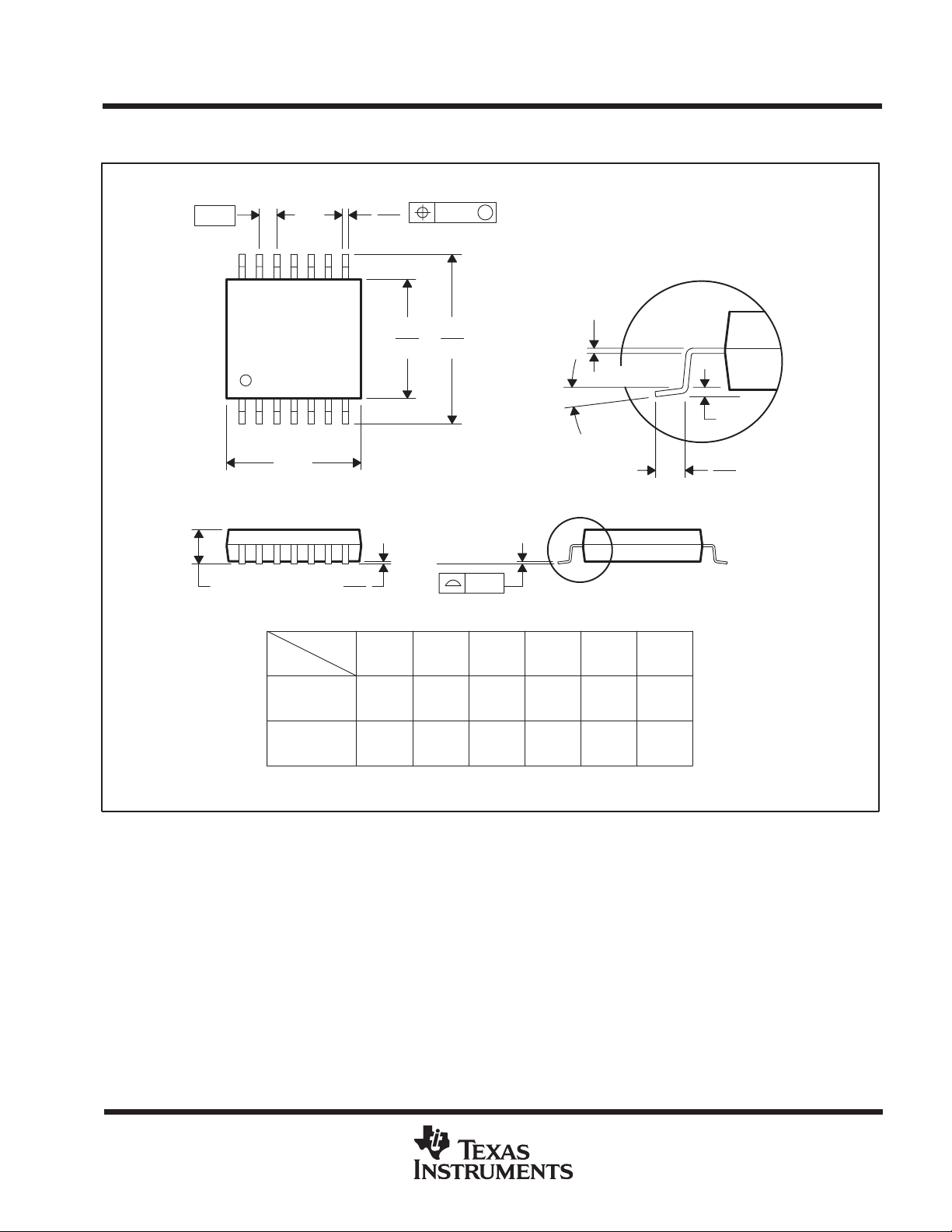
PACKAGE DRAWING
PW (R-PDSO-G**) PLASTIC SMALL-OUTLINE PACKAGE
14 PINS SHOWN
0,65
1,20 MAX
14
0,30
0,19
8
4,50
4,30
PINS **
7
Seating Plane
0,15
0,05
8
1
A
DIM
14
0,10
6,60
6,20
M
0,10
0,15 NOM
0°–8°
2016
Gage Plane
24
0,25
0,75
0,50
28
A MAX
A MIN
NOTES: A. All linear dimensions are in millimeters.
B. This drawing is subject to change without notice.
C. Body dimensions do not include mold flash or protrusion not to exceed 0,15.
D. Falls within JEDEC MO-153
3,10
2,90
5,10
4,90
5,10
4,90
6,60
6,40
7,90
7,70
9,80
9,60
4040064/F 01/97
20
www.ti.com
DIT4096
SBOS225A
Page 21

PACKAGE OPTION ADDENDUM
www.ti.com
6-Dec-2006
PACKAGING INFORMATION
Orderable Device Status
(1)
Package
Type
Package
Drawing
Pins Package
Qty
Eco Plan
DIT4096IPW ACTIVE TSSOP PW 28 50 Green (RoHS &
no Sb/Br)
DIT4096IPWG4 ACTIVE TSSOP PW 28 50 Green (RoHS &
no Sb/Br)
DIT4096IPWR ACTIVE TSSOP PW 28 2000 Green (RoHS &
no Sb/Br)
DIT4096IPWRG4 ACTIVE TSSOP PW 28 2000 Green (RoHS &
no Sb/Br)
(1)
The marketing status values are defined as follows:
ACTIVE: Product device recommended for new designs.
LIFEBUY: TI has announced that the device will be discontinued, and a lifetime-buy period is in effect.
NRND: Not recommended for new designs. Device is in production to support existing customers, but TI does not recommend using this part in
a new design.
PREVIEW: Device has been announced but is not in production. Samples may or may not be available.
OBSOLETE: TI has discontinued the production of the device.
(2)
Eco Plan - The planned eco-friendly classification: Pb-Free (RoHS), Pb-Free (RoHS Exempt), or Green (RoHS & no Sb/Br) - please check
http://www.ti.com/productcontent for the latest availability information and additional product content details.
TBD: The Pb-Free/Green conversion plan has not been defined.
Pb-Free (RoHS): TI's terms "Lead-Free" or "Pb-Free" mean semiconductor products that are compatible with the current RoHS requirements
for all 6 substances, including the requirement that lead not exceed 0.1% by weight in homogeneous materials. Where designed to be soldered
at high temperatures, TI Pb-Free products are suitable for use in specified lead-free processes.
Pb-Free (RoHS Exempt): This component has a RoHS exemption for either 1) lead-based flip-chip solder bumps used between the die and
package, or 2) lead-based die adhesive used between the die and leadframe. The component is otherwise considered Pb-Free (RoHS
compatible) as defined above.
Green (RoHS & no Sb/Br): TI defines "Green" to mean Pb-Free (RoHS compatible), and free of Bromine (Br) and Antimony (Sb) based flame
retardants (Br or Sb do not exceed 0.1% by weight in homogeneous material)
(2)
Lead/Ball Finish MSLPeak Temp
CU NIPDAU Level-1-260C-UNLIM
CU NIPDAU Level-1-260C-UNLIM
CU NIPDAU Level-1-260C-UNLIM
CU NIPDAU Level-1-260C-UNLIM
(3)
(3)
MSL, Peak Temp. -- The Moisture Sensitivity Level rating according to the JEDEC industry standard classifications, and peak solder
temperature.
Important Information and Disclaimer:The information provided on this page represents TI's knowledge and belief as of the date that it is
provided. TI bases its knowledge and belief on information provided by third parties, and makes no representation or warranty as to the
accuracy of such information. Efforts are underway to better integrate information from third parties. TI has taken and continues to take
reasonable steps to provide representative and accurate information but may not have conducted destructive testing or chemical analysis on
incoming materials and chemicals. TI and TI suppliers consider certain information to be proprietary, and thus CAS numbers and other limited
information may not be available for release.
In no event shall TI's liability arising out of such information exceed the total purchase price of the TI part(s) at issue in this document sold by TI
to Customer on an annual basis.
Addendum-Page 1
Page 22

PACKAGE MATERIALS INFORMATION
www.ti.com
TAPE AND REEL INFORMATION
11-Mar-2008
*All dimensions are nominal
Device Package
Type
DIT4096IPWR TSSOP PW 28 2000 330.0 16.4 6.9 10.2 1.8 12.0 16.0 Q1
Package
Drawing
Pins SPQ Reel
Diameter
(mm)
Reel
Width
W1 (mm)
A0 (mm) B0 (mm) K0 (mm) P1
(mm)W(mm)
Pin1
Quadrant
Pack Materials-Page 1
Page 23
PACKAGE MATERIALS INFORMATION
www.ti.com
11-Mar-2008
*All dimensions are nominal
Device Package Type Package Drawing Pins SPQ Length (mm) Width (mm) Height (mm)
DIT4096IPWR TSSOP PW 28 2000 346.0 346.0 33.0
Pack Materials-Page 2
Page 24
MECHANICAL DATA
MTSS001C – JANUARY 1995 – REVISED FEBRUARY 1999
PW (R-PDSO-G**) PLASTIC SMALL-OUTLINE PACKAGE
14 PINS SHOWN
0,65
1,20 MAX
14
0,30
0,19
8
4,50
4,30
PINS **
7
Seating Plane
0,15
0,05
8
1
A
DIM
6,60
6,20
14
0,10
0,10
M
0,15 NOM
Gage Plane
0,25
0°–8°
2016
24
28
0,75
0,50
A MAX
A MIN
NOTES: A. All linear dimensions are in millimeters.
B. This drawing is subject to change without notice.
C. Body dimensions do not include mold flash or protrusion not to exceed 0,15.
D. Falls within JEDEC MO-153
3,10
2,90
5,10
4,90
5,10
4,90
6,60
6,40
7,90
7,70
9,80
9,60
4040064/F 01/97
POST OFFICE BOX 655303 • DALLAS, TEXAS 75265
Page 25

IMPORTANT NOTICE
Texas Instruments Incorporated and its subsidiaries (TI) reserve the right to make corrections, modifications, enhancements, improvements,
and other changes to its products and services at any time and to discontinue any product or service without notice. Customers should
obtain the latest relevant information before placing orders and should verify that such information is current and complete. All products are
sold subject to TI’s terms and conditions of sale supplied at the time of order acknowledgment.
TI warrants performance of its hardware products to the specifications applicable at the time of sale in accordance with TI’s standard
warranty. Testing and other quality control techniques are used to the extent TI deems necessary to support this warranty. Except where
mandated by government requirements, testing of all parameters of each product is not necessarily performed.
TI assumes no liability for applications assistance or customer product design. Customers are responsible for their products and
applications using TI components. To minimize the risks associated with customer products and applications, customers should provide
adequate design and operating safeguards.
TI does not warrant or represent that any license, either express or implied, is granted under any TI patent right, copyright, mask work right,
or other TI intellectual property right relating to any combination, machine, or process in which TI products or services are used. Information
published by TI regarding third-party products or services does not constitute a license from TI to use such products or services or a
warranty or endorsement thereof. Use of such information may require a license from a third party under the patents or other intellectual
property of the third party, or a license from TI under the patents or other intellectual property of TI.
Reproduction of TI information in TI data books or data sheets is permissible only if reproduction is without alteration and is accompanied
by all associated warranties, conditions, limitations, and notices. Reproduction of this information with alteration is an unfair and deceptive
business practice. TI is not responsible or liable for such altered documentation. Information of third parties may be subject to additional
restrictions.
Resale of TI products or services with statements different from or beyond the parameters stated by TI for that product or service voids all
express and any implied warranties for the associated TI product or service and is an unfair and deceptive business practice. TI is not
responsible or liable for any such statements.
TI products are not authorized for use in safety-critical applications (such as life support) where a failure of the TI product would reasonably
be expected to cause severe personal injury or death, unless officers of the parties have executed an agreement specifically governing
such use. Buyers represent that they have all necessary expertise in the safety and regulatory ramifications of their applications, and
acknowledge and agree that they are solely responsible for all legal, regulatory and safety-related requirements concerning their products
and any use of TI products in such safety-critical applications, notwithstanding any applications-related information or support that may be
provided by TI. Further, Buyers must fully indemnify TI and its representatives against any damages arising out of the use of TI products in
such safety-critical applications.
TI products are neither designed nor intended for use in military/aerospace applications or environments unless the TI products are
specifically designated by TI as military-grade or "enhanced plastic." Only products designated by TI as military-grade meet military
specifications. Buyers acknowledge and agree that any such use of TI products which TI has not designated as military-grade is solely at
the Buyer's risk, and that they are solely responsible for compliance with all legal and regulatory requirements in connection with such use.
TI products are neither designed nor intended for use in automotive applications or environments unless the specific TI products are
designated by TI as compliant with ISO/TS 16949 requirements. Buyers acknowledge and agree that, if they use any non-designated
products in automotive applications, TI will not be responsible for any failure to meet such requirements.
Following are URLs where you can obtain information on other Texas Instruments products and application solutions:
Products Applications
Amplifiers amplifier.ti.com Audio www.ti.com/audio
Data Converters dataconverter.ti.com Automotive www.ti.com/automotive
DSP dsp.ti.com Broadband www.ti.com/broadband
Clocks and Timers www.ti.com/clocks Digital Control www.ti.com/digitalcontrol
Interface interface.ti.com Medical www.ti.com/medical
Logic logic.ti.com Military www.ti.com/military
Power Mgmt power.ti.com Optical Networking www.ti.com/opticalnetwork
Microcontrollers microcontroller.ti.com Security www.ti.com/security
RFID www.ti-rfid.com Telephony www.ti.com/telephony
RF/IF and ZigBee® Solutions www.ti.com/lprf Video & Imaging www.ti.com/video
Mailing Address: Texas Instruments, Post Office Box 655303, Dallas, Texas 75265
Copyright © 2008, Texas Instruments Incorporated
Wireless www.ti.com/wireless
 Loading...