www.ti.com
Resistor
Network
8
14
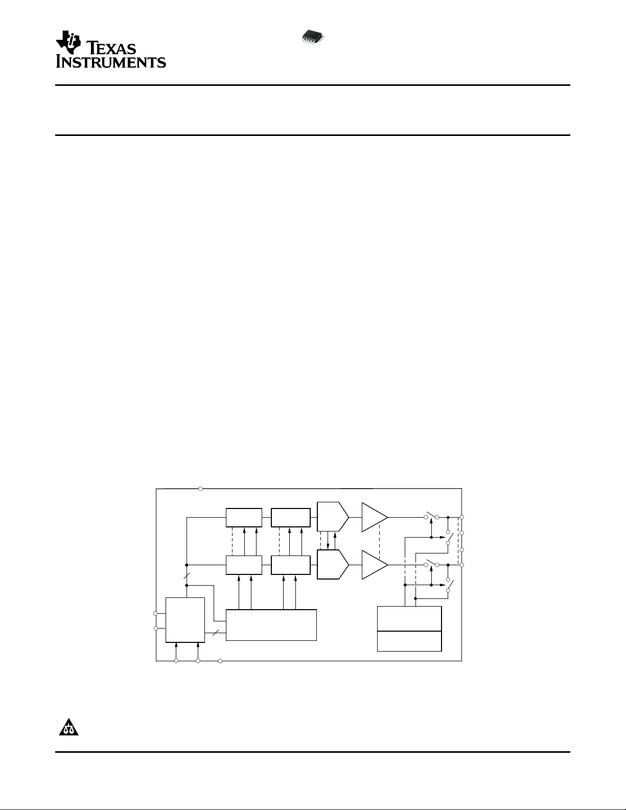
Data
Buffer A
DAC
Register A
Data
Buffer D
DAC
Register D
DAC A
DAC D
Buffer
Control
Register
Control
Power-Down
Control Logic
V
OUT
A
V
OUT
B
V
OUT
C
V
OUT
D
A0 A1 GND
I2C
Block
SCL
SDA
V
DD
QUAD, 8-BIT, LOW-POWER, VOLTAGE OUTPUT,
I2C INTERFACE DIGITAL-TO-ANALOG CONVERTER
FEATURES DESCRIPTION
• Micropower Operation: 500 µA at 3 V V
• Fast Update Rate: 188 kSPS
• Per-channel Power-down Capability
• Power-On Reset to Zero
• 2.7-V to 5.5-V Analog Power Supply
• 8-bit Monotonic
• I2C™ Interface Up to 3.4 Mbps
• Data Transmit Capability
• On-Chip Output Buffer Amplifier, Rail-to-Rail
Operation
• Double-Buffered Input Register
• Address Support for up to Four DAC5574s
• Synchronous Update Support for up to 16
Channels
• Operation From –40 ° C to 105 ° C
• Small 10 Lead MSOP Package
APPLICATIONS
• Process Control
• Data Acquisition Systems
• Closed-Loop Servo Control
• PC Peripherals
• Portable Instrumentation
DAC5574
SLAS407 – DECEMBER 2003
DD
The DAC5574 is a low-power, quad channel, 8-bit
buffered voltage output DAC. Its on-chip precision
output amplifier allows rail-to-rail output swing to be
achieved. The DAC5574 utilizes an I2C compatible
two wire serial interface supporting high-speed
interface mode with address support of up to four
DAC5574s for a total of 16 channels on the bus.
The DAC5574 uses V
and GND to set the output
DD
range of the DAC. The DAC5574 incorporates a
power-on-reset circuit that ensures that the DAC
output powers up at zero volts and remains there until
a valid write takes place to the device. The DAC5574
contains a per-channel power-down feature, accessed via the internal control register, reducing the
current consumption of the device to 200 nA at 5 V.
The low power consumption of this part in normal
operation makes it ideally suited to portable battery
operated equipment. The power consumption is less
than 3mW at V
= 5 V reducing to 1 µW in
DD
power-down mode.
TI offers a variety of data converters with I2C
interface. See DACx57x family of 16/12/10/8 bit,
single and quad channel DACs. Also see ADS7823
and ADS1100, 12-bit octal channel and 16-bit single
channel ADCs.
I2C is a trademark of Philips Corporation.
PRODUCTION DATA information is current as of publication date.
Products conform to specifications per the terms of the Texas
Instruments standard warranty. Production processing does not
necessarily include testing of all parameters.
Please be aware that an important notice concerning availability, standard warranty, and use in critical applications of Texas
Instruments semiconductor products and disclaimers thereto appears at the end of this data sheet.
Copyright © 2003, Texas Instruments Incorporated
www.ti.com
A1
A0
1
2
3
4
5 6
7
8
10
9
V
OUT
A
V
OUT
B
GND
V
OUT
C
V
OUT
D
V
DD
SDA
SCL
DAC5574
.
DAC5574
SLAS407 – DECEMBER 2003
This integrated circuit can be damaged by ESD. Texas Instruments recommends that all integrated
circuits be handled with appropriate precautions. Failure to observe proper handling and installation
procedures can cause damage.
ESD damage can range from subtle performance degradation to complete device failure. Precision
integrated circuits may be more susceptible to damage because very small parametric changes could
cause the device not to meet its published specifications.
PACKAGE/ORDERING INFORMATION
PRODUCT PACKAGE PACKAGE SPECIFICATION PACKAGE ORDERING TRANSPORT MEDIA
DAC5574 10-MSOP DGS –40 °C TO +105 °C D574 DAC5574IDGS 80 Piece Tube
(1) For the most current package and ordering information, see the Package Option Addendum at the end of this document, or see the TI
website at www.ti.com .
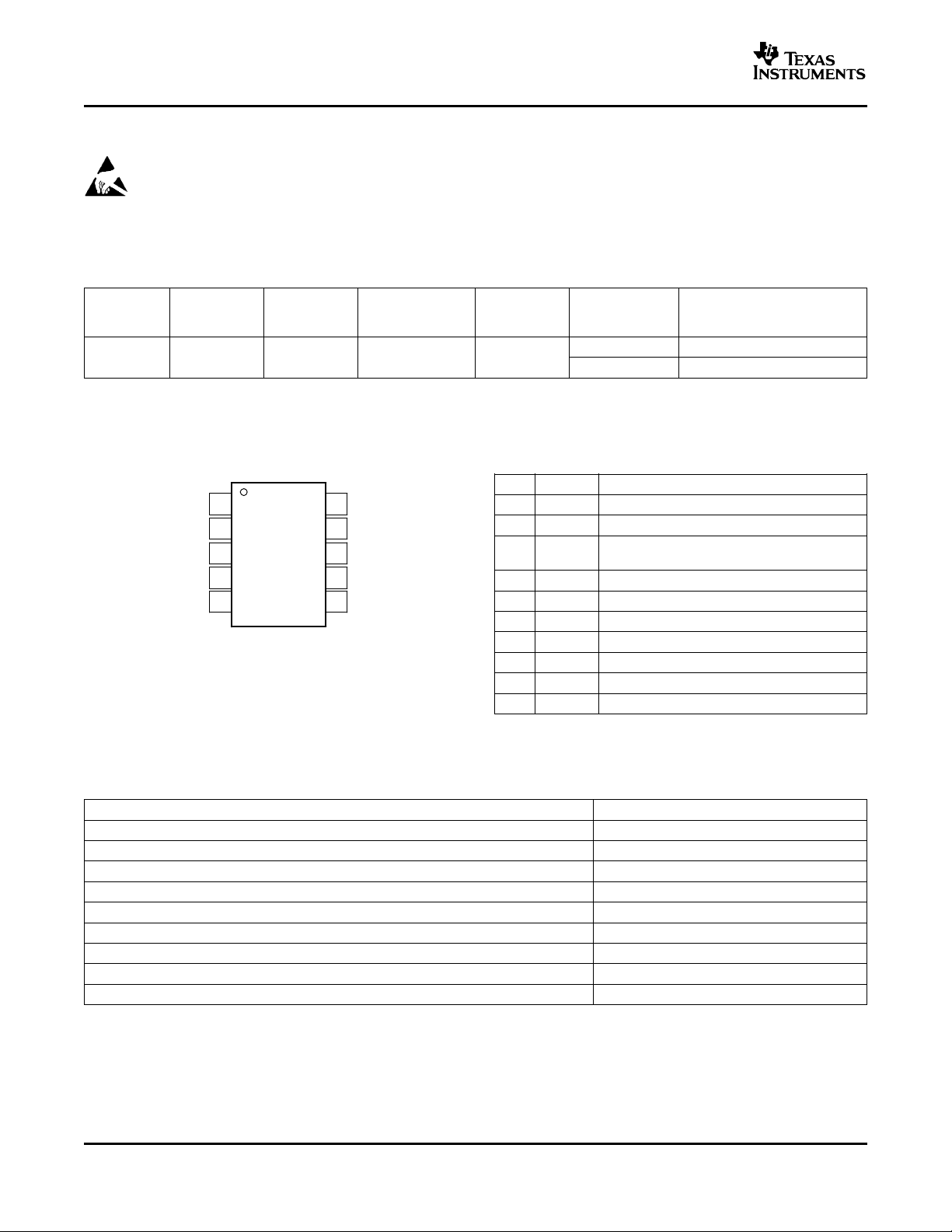
DGS PACKAGE
DRAWING TEMPERATURE MARKING NUMBER
NUMBER RANGE
(TOPVIEW)
PIN NAME DESCRIPTION
1 V
OUT
2 V
OUT
3 GND
4 V
OUT
5 V
OUT
6 SCL Serial clock input
7 SDA Serial data input and output
8 V
9 A0 Device address select - I2C
10 A1 Device address select - I2C
(1)
DAC5574IDGSR 2500 Piece Tape and Reel
PIN DESCRIPTIONS
A Analog output voltage from DAC A
B Analog output voltage from DAC B
Ground reference point for all circuitry on the
part
C Analog output voltage from DAC C
D Analog output voltage from DAC D
Analog voltage supply input
DD
ABSOLUTE MAXIMUM RATINGS
V
to GND –0.3 V to +6 V
DD
Digital input voltage to GND –0.3 V to V
V
OUT
Operating temperature range –40 °C to +105 °C
Storage temperature range –65 °C to +150 °C
Junction temperature range (T
Power dissipation: Thermal impedance ( ΘJA) 270 °C/W
Lead temperature, soldering: Vapor phase (60s) 215 °C
(1) Stresses above those listed under Absolute Maximum Ratings may cause permanent damage to the device. Exposure to absolute
maximum conditions for extended periods may affect device reliability.
2
(1)
to GND –0.3 V to V
max) +150 °C
J
Thermal impedance ( ΘJC) 77 °C/W
Infrared (15s) 220 °C
+ 0.3 V
DD
+ 0.3 V
DD
www.ti.com
DAC5574
SLAS407 – DECEMBER 2003
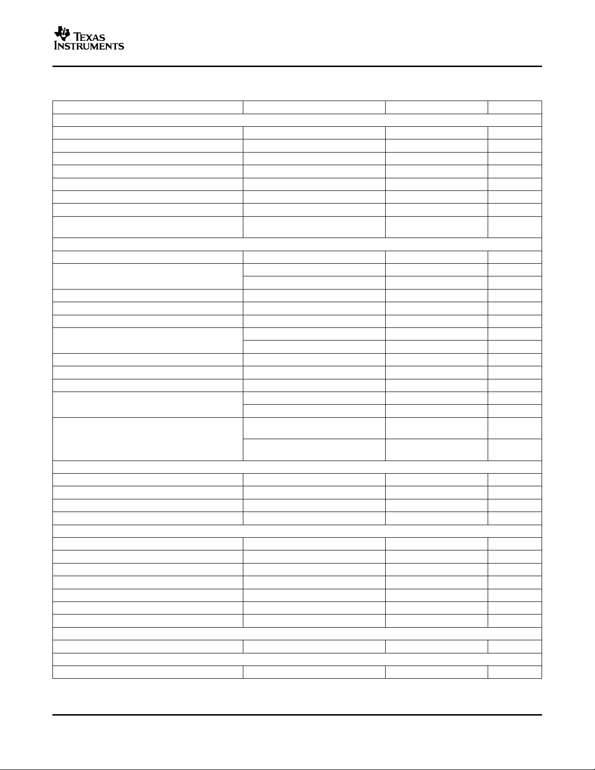
ELECTRICAL CHARACTERISTICS
V
= 2.7 V to 5.5 V, RL= 2 k Ω to GND; CL= 200 pF to GND; all specifications –40 ° C to +105 ° C, unless otherwise specified.
DD
PARAMETER TEST CONDITIONS MIN TYP MAX UNITS
STATIC PERFORMANCE
Resolution 8 Bits
Relative accuracy ± 0.15 ± 0.5 LSB
Differential nonlinearity Specified monotonic by design ± 0.02 ± 0.25 LSB
Zero-scale error 5 20 mV
Full-scale error -0.15 ± 1.0 % of FSR
Gain error ± 1.0 % of FSR
Zero code error drift ± 7 µV/ °C
Gain temperature coefficient ± 3 ppm of
OUTPUT CHARACTERISTICS
Output voltage range 0 V
Output voltage settling time (full scale) RL= ∞ ; 0 pF < CL< 200 pF 6 8 µs
Slew rate 1 V/ µs
dc crosstalk (channel-to-channel) 0.0025 LSB
ac crosstalk (channel-to-channel) 1 kHz Sine Wave -100 dB
Capacitive load stability RL= ∞ 470 pF
Digital-to-analog glitch impulse 1 LSB change around major carry 12 nV-s
Digital feedthrough 0.3 nV-s
dc output impedance 1 Ω
Short-circuit current VDD= 5 V 50 mA
Power-up time Coming out of power-down mode, 2.5 µs
LOGIC INPUTS
(2)
Input current ± 1 µA
V
, Input low voltage 0.3xV
IN_L
V
, Input high voltage VDD= 3 V 0.7xV
IN_H
Pin Capacitance 3 pF
POWER REQUIREMENTS
V
DD
IDD(normal operation), including reference current Excluding load current
IDD@ VDD=+3.6V to +5.5V VIH= V
IDD@ V
IDD(all power-down modes)
IDD@ VDD=+3.6V to +5.5V VIH= V
IDD@ V
POWER EFFICIENCY
I
/I
OUT
DD
TEMPERATURE RANGE
Specified performance -40 +105 °C
(1) Linearity tested using a reduced code range of 48 to 4047; output unloaded.
(2) Specified by design and characterization, not production tested.
(1)
(2)
Coming out of power-down mode, 5 µs
=+2.7V to +3.6V VIH= V
DD
=+2.7V to +3.6V VIH= V
DD
DD
RL= ∞ ; CL= 500 pF 12 µs
RL= 2 k Ω 1000 pF
VDD= 3 V 20 mA
VDD= +5 V
VDD= +3 V
DD
DD
2.7 5.5 V
and VIL=GND 600 900 µA
DD
and VIL=GND 500 750 µA
DD
and VIL=GND 0.2 1 µA
DD
and VIL=GND 0.05 1 µA
DD
I
= 2 mA, VDD= +5 V 93%
LOAD
FSR/ °C
V
V
V
3
www.ti.com
DAC5574
SLAS407 – DECEMBER 2003
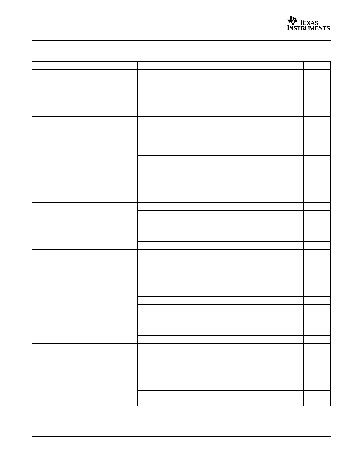
TIMING CHARACTERISTICS
V
= 2.7 V to 5.5 V, RL= 2 k Ω to GND; all specifications –40 ° C to +105 ° C, unless otherwise specified.
DD
SYMBOL PARAMETER TEST CONDITIONS MIN TYP MAX UNITS
Standard mode 100 kHz
Fast mode 400 kHz
Standard mode 4.7 µs
Fast mode 1.3 µs
Standard mode 4.0 µs
Fast mode 600 ns
High-speed mode 160 ns
Standard mode 4.7 µs
Fast mode 1.3 µs
Standard mode 4.0 µs
Fast mode 600 ns
Standard mode 4.7 µs
Fast mode 600 ns
High-speed mode 160 ns
Standard mode 250 ns
High-speed mode 10 ns
Standard mode 0 3.45 µs
Fast mode 0 0.9 µs
Standard mode 1000 ns
Fast mode 20 + 0.1C
B
Standard mode 1000 ns
Fast mode 20 + 0.1C
B
Standard mode 300 ns
Fast mode 20 + 0.1C
B
Standard mode 1000 ns
Fast mode 20 + 0.1C
B
tHD; t
tSU; t
tSU; t
tHD; t
f
SCL
SCL clock frequency
High-Speed Mode, CB= 100 pF max 3.4 MHz
High-speed mode, CB= 400 pF max 1.7 MHz
t
BUF
STA
t
LOW
Bus free time between a
STOP and START condition
Hold time (repeated) START
condition
LOW period of the SCL clock
High-speed mode, CB= 100 pF max 160 ns
High-speed mode, CB= 400 pF max 320 ns
t
HIGH
HIGH period of the SCL clock
High-Speed Mode, CB= 100 pF max 60 ns
High-speed mode, CB= 400 pF max 120 ns
STA
DAT
DAT
Setup time for a repeated
START condition
Data setup time Fast mode 100 ns
Data hold time
High-speed mode, CB= 100 pF max 0 70 ns
High-speed mode, CB= 400 pF max 0 150 ns
t
RCL
Rise time of SCL signal
High-speed mode, CB= 100 pF max 10 40 ns
High-speed mode, CB= 400 pF max 20 80 ns
Rise time of SCL signal after
t
RCL1
t
FCL
a repeated START condition
and after an acknowledge
Fall time of SCL signal
BIT
High-speed mode, CB= 100 pF max 10 80 ns
High-speed mode, CB= 400 pF max 20 160 ns
High-speed mode, CB= 100 pF max 10 40 ns
High-speed mode, CB= 400 pF max 20 80 ns
t
RDA
Rise time of SDA signal
High-speed mode, CB= 100 pF max 10 80 ns
High-speed mode, CB= 400 pF max 20 160 ns
300 ns
300 ns
300 ns
300 ns
4
www.ti.com
−1
−0.5
0
0.5
1
−0.5
−0.25
0
0.25
0.5
0 32 64 96 128 160 192 224
Digital Input Code
Channel AChannel A VDD = 5 V
255
LE − LSBDLE − LSB
−1
−0.5
0
0.5
1
−0.5
−0.25
0
0.25
0.5
0 32 64 96 128 160 192 224
Digital Input Code
Channel B VDD = 5 V
255
LE − LSBDLE − LSB
TIMING CHARACTERISTICS (continued)
V
= 2.7 V to 5.5 V, RL= 2 k Ω to GND; all specifications –40 ° C to +105 ° C, unless otherwise specified.
DD
SYMBOL PARAMETER TEST CONDITIONS MIN TYP MAX UNITS
Standard mode 300 ns
tSU; t
t
FDA
Fall time of SDA signal
High-speed mode, CB= 100 pF max 10 80 ns
Fast mode 20 + 0.1C
High-speed mode, CB= 400 pF max 20 160 ns
Standard mode 4.0 µs
STO
Setup time for STOP con-
dition
Fast mode 600 ns
High-speed mode 160 ns
C
B
t
SP
V
NH
V
NL
Capacitive load for SDA and
SCL
Pulse width of spike sup-
pressed
Noise margin at the HIGH
Fast mode 50 ns
High-speed mode 10 ns
Standard mode
level for each connected de- Fast mode 0.2 V
vice (including hysteresis)
Noise margin at the LOW
High-speed mode
Standard mode
level for each connected de- Fast mode 0.1 V
vice (including hysteresis)
High-speed mode
B
DD
DD
DAC5574
SLAS407 – DECEMBER 2003
300 ns
400 pF
V
V
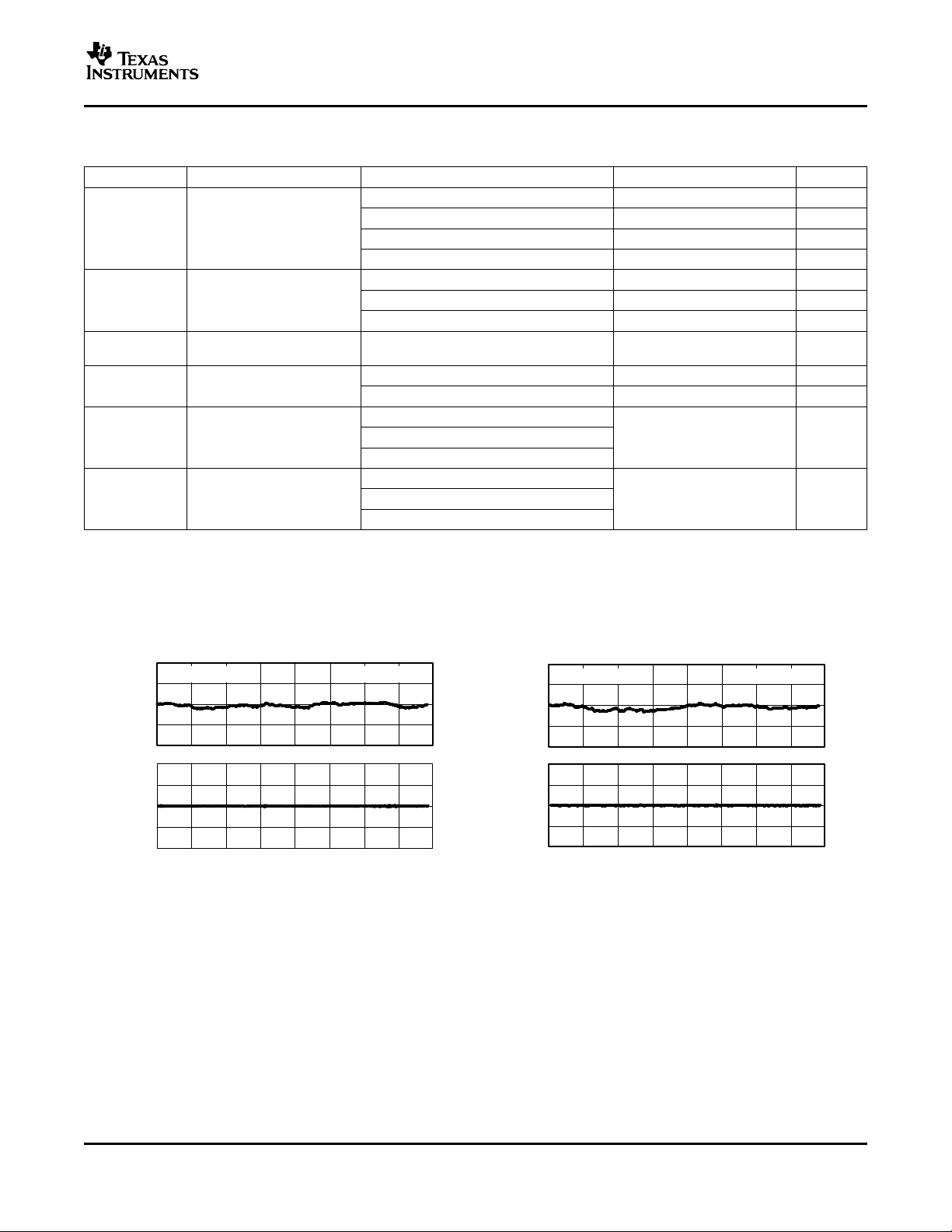
LINEARITY ERROR AND DIFFERENTIAL LINEARITY ERROR AND DIFFERENTIAL
LINEARITY ERROR vs DIGITAL INPUT CODE LINEARITY ERROR vs DIGITAL INPUT CODE
TYPICAL CHARACTERISTICS
At TA= +25 ° C, unless otherwise noted.
Figure 1. Figure 2.
5
www.ti.com
−1
−0.5
0
0.5
1
LE − LSB
−0.5
−0.25
0
0.25
0.5
0 32 64 96 128 160 192 224
Digital Input Code
DLE − LSB
255
Channel D
VDD = 5 V
−1
−0.5
0
0.5
1
LE − LSB
−0.5
−0.25
0
0.25
0.5
0 32 64 96 128 160 192 224
Digital Input Code
DLE − LSB
255
Channel C VDD = 5 V
−1
−0.5
0
0.5
1
−0.5
−0.25
0
0.25
0.5
0 32 64 96 128 160 192 224
Digital Input Code
255
LE − LSBDLE − LSB
Channel A
VDD = 2.7 V
−1
−0.5
0
0.5
1
LE − LSB
−0.5
−0.25
0
0.25
0.5
0 32 64 96 128 160 192 224
Digital Input Code
DLE − LSB
255
Channel B
VDD = 2.7 V
−1
−0.5
0
0.5
1
−0.5
−0.25
0
0.25
0.5
0 32 64 96 128 160 192 224
Digital Input Code
255
LE − LSBDLE − LSB
Channel D
VDD = 2.7 V
−1
−0.5
0
0.5
1
−0.5
−0.25
0
0.25
0.5
0 32 64 96 128 160 192 224
Digital Input Code
255
LE − LSBDLE − LSB
Channel C
VDD = 2.7 V
DAC5574
SLAS407 – DECEMBER 2003
TYPICAL CHARACTERISTICS (continued)
At TA= +25 ° C, unless otherwise noted.
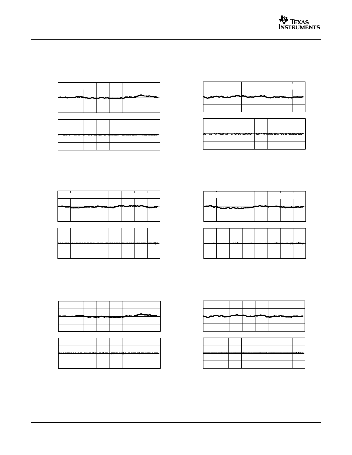
LINEARITY ERROR AND DIFFERENTIAL LINEARITY ERROR AND DIFFERENTIAL
LINEARITY ERROR vs DIGITAL INPUT CODE LINEARITY ERROR vs DIGITAL INPUT CODE
LINEARITY ERROR AND DIFFERENTIAL LINEARITY ERROR AND DIFFERENTIAL
LINEARITY ERROR vs DIGITAL INPUT CODE LINEARITY ERROR vs DIGITAL INPUT CODE
Figure 3. Figure 4.
LINEARITY ERROR AND DIFFERENTIAL LINEARITY ERROR AND DIFFERENTIAL
LINEARITY ERROR vs DIGITAL INPUT CODE LINEARITY ERROR vs DIGITAL INPUT CODE
6
Figure 5. Figure 6.
Figure 7. Figure 8.
www.ti.com
5
10
15
20
−40 −10 20 50 80
TA − Free−Air T emperature − °C
Zero-Scale Error − mV
VDD = 5 V
CH A
CH B
CH C
CH D
0
5
10
15
−40 −10 20 50 80
TA − Free−Air T emperature − °C
Zero-Scale Error − mV
VDD = 2.7 V
CH A
CH B
CH C
CH D
0
5
10
15
20
25
30
−40 −10 20 50 80
CH A
CH B
CH D
T
A
− Free−Air T emperature − °C
Full-Scale Error − mV
VDD = 5 V
CH C
0
5
10
15
20
−40 −10 20 50 80
TA − Free−Air T emperature − °C
Full-Scale Error − mV
VDD = 2.7 V
CH A
CH B
CH C
CH D
0.000
0.025
0.050
0.075
0.100
0.125
0.150
0 1 2 3 4 5
I
SINK
− Sink Current − mA
V
OUT
− Output Voltage − V
VDD = 2.7 V
VDD = 5.5 V
DAC Loaded With 00
H
Typical For All Channels
5.30
5.35
5.40
5.45
5.50
0 1 2 3 4 5
I
SOURCE
− Source Current − mA
V
OUT
− Output Voltage − V
DAC Loaded With FF
H
VDD = 5.5 V
Typical For All Channels
TYPICAL CHARACTERISTICS (continued)
At TA= +25 ° C, unless otherwise noted.
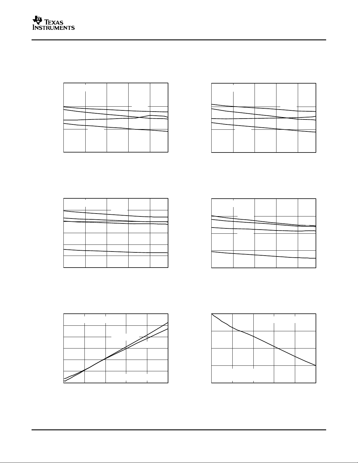
ZERO-SCALE ERROR ZERO-SCALE ERROR
FULL-SCALE ERROR FULL-SCALE ERROR
DAC5574
SLAS407 – DECEMBER 2003
vs TEMPERATURE vs TEMPERATURE
Figure 9. Figure 10.
vs TEMPERATURE vs TEMPERATURE
Figure 11. Figure 12.
SINK CURRENT CAPABILITY SOURCE CURRENT CAPABILITY
AT NEGATIVE RAIL AT POSITIVE RAIL
Figure 13. Figure 14.
7
www.ti.com
2.3
2.4
2.5
2.6
2.7
0 1 2 3 4 5
I
SOURCE
− Source Current − mA
V
OUT
− Output Voltage − V
DAC Loaded With FF
H
VDD = 2.7 V
Typical For All Channels
Digital Input Code
0
100
200
300
400
500
600
700
800
0 32 64 96 128 160 192 224
I
DD
− Supply Current − µA
VDD = 2.7 V
VDD = 5.5 V
All Channels Powered, No Load
255
TA − Free−Air T emperature − °C
0
100
200
300
400
500
600
700
−40 −10 20 50 80 110
I
DD
− Supply Current − µA
VDD = 2.7 V
VDD = 5.5 V
All Channels Powered, No Load
VDD − Supply Voltage − V
200
250
300
350
400
450
500
550
600
650
700
2.7 3.1 3.5 3.9 4.3 4.7 5.1 5.5
I
DD
− Supply Current − µA
All DACs Powered, No Load
IDD − Current Consumption − µA
0
500
1000
1500
2000
500 520 540 560 580 600 620 640 660 680 700 720 740
VDD = 5 V
Frequency
V
Logic
− Logic Input Voltage − V
200
400
600
800
1000
1200
0 1 2 3 4 5
I
DD
− Supply Current − µA
TA = 25°C
A0 Input (All Other Inputs = GND)
VDD = 2.7 V
VDD = 5.5 V
DAC5574
SLAS407 – DECEMBER 2003
TYPICAL CHARACTERISTICS (continued)
At TA= +25 ° C, unless otherwise noted.
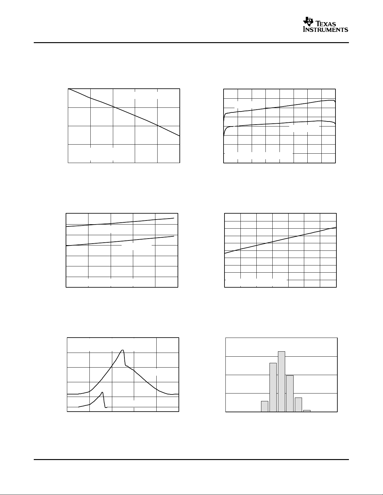
SOURCE CURRENT CAPABILITY SUPPLY CURRENT
AT POSITIVE RAIL vs DIGITAL INPUT CODE
Figure 15. Figure 16.
SUPPLY CURRENT SUPPLY CURRENT
vs TEMPERATURE vs SUPPLY VOLTAGE
SUPPLY CURRENT HISTOGRAM
vs LOGIC INPUT VOLTAGE OF CURRENT CONSUMPTION
8
Figure 17. Figure 18.
Figure 19. Figure 20.
www.ti.com
−1
0
1
2
3
4
5
6
Time (2 µs/div)
V
OUT
− Output Voltage − V
VDD = 5 V
Powerup to Code 250
IDD − Current Consumption − µA
0
500
1000
1500
2000
400 420 440 460 480 500 520 540 560 580 600 620
VDD = 2.7 V
Frequency
0
1
2
3
4
5
Time (25 µs/div)
V
OUT
− Output Voltage − V
VDD = 5 V
Output Loaded with
200 pF to GND
10% to 90% FSR
0.0
0.5
1.0
1.5
2.0
2.5
3.0
Time (25 µs/div)
V
OUT
− Output Voltage − V
VDD = 2.7 V
Output Loaded with
200 pF to GND
10% to 90% FSR
0
4
8
12
16
20
24
0 32 64 96 128 160 192 224
Digital Input Code
Output Error (mV)
255
Channel A Output
Channel D Output
Channel B Output
Channel C Output
VDD = 5 V, TA = 25°C
−6
−2
2
6
10
14
18
0 32 64 96 128 160 192 224 255
Channel A Output
VDD = 2.7 V, TA = 25°C
Channel D Output
Channel C Output
Channel B Output
Digital Input Code
Output Error (mV)
TYPICAL CHARACTERISTICS (continued)
At TA= +25 ° C, unless otherwise noted.
DAC5574
SLAS407 – DECEMBER 2003
OF CURRENT CONSUMPTION POWER-DOWN MODE
HISTOGRAM EXITING
Figure 21. Figure 22.
LARGE SIGNAL LARGE SIGNAL
SETTLING TIME SETTLING TIME
ABSOLUTE ERROR
†
linearity.
Absolute error is the deviation from ideal DAC characteristics. It includes affects of offset, gain, and integral
Figure 23. Figure 24.
†
ABSOLUTE ERROR
Figure 25. Figure 26.
†
9
 Loading...