

Page 1

DAC3283
www.ti.com
Dual-Channel, 16-Bit, 800 MSPS, Digital-to-Analog Converter (DAC)
Check for Samples: DAC3283
1
FEATURES
• Dual, 16-Bit, 800 MSPS DACs
• 8-Bit Input LVDS Data Bus
– Byte-Wide Interleaved Data Load
– 8 Sample Input FIFO
– Optional Data Pattern Checker
• Multi-DAC Synchronization
• Selectable 2x-4x Interpolation Filters
– Stop-Band Attenuation > 85 dB
• Fs/2 and ± Fs/4 Coarse Mixer
• Digital Quadrature Modulator Correction
– Gain, Phase and Offset Correction
• Temperature Sensor
• 3- or 4-Wire Serial Control Interface
• On-Chip 1.2-V Reference
• Differential Scalable Output: 2 to 20 mA
• Single-Carrier TM1 WCDMA ACLR: 82 dBc at
f
= 122.88 MHz
OUT
• Low Power: 1.3 W at 800 MSPS
• Space Saving Package: 48-pin 7×7mm QFN
SLAS693A –MARCH 2010–REVISED APRIL 2010
APPLICATIONS
• Cellular Base Stations
• Diversity Transmit
• Wideband Communications
• Digital Synthesis
DESCRIPTION
The DAC3283 is a dual-channel 16-bit 800 MSPS
digital-to-analog converter (DAC) with an 8-bit LVDS
input data bus with on-chip termination, optional
2x-4x interpolation filters, digital IQ compensation and
internal voltage reference. The DAC3283 offers
superior linearity, noise and crosstalk performance.
Input data can be interpolated by 2x or 4x through
on-chip interpolating FIR filters with over 85 dB of
stop-band attenuation. Multiple DAC3283 devices can
be fully synchronized.
The DAC3283 allows either a complex or real output.
An optional coarse mixer in complex mode provides
frequency upconversion and the dual DAC output
produces a complex Hilbert Transform pair. The
digital IQ compensation feature allows optimization of
phase, gain and offset to maximize sideband rejection
and minimize LO feed-through of an external
quadrature modulator performing the final single
sideband RF up-conversion.
The DAC3283 is characterized for operation over the
entire industrial temperature range of –40°C to 85°C
and is available in a 48-pin 7×7mm QFN package.
ORDERING INFORMATION
T
A
–40°C to 85°C RGZ/64QFN Quad Flatpack No-Lead Tape and Reel
(1) Thermal Pad Size: 5,6 mm × 5,6 mm
(2) MSL Peak Temperature: Level-3-260C-168 HR
(3) For the most current package and ordering information, see the Package Option Addendum at the end of this document, or see the TI
website at www.ti.com.
1
Please be aware that an important notice concerning availability, standard warranty, and use in critical applications of Texas
Instruments semiconductor products and disclaimers thereto appears at the end of this data sheet.
PRODUCTION DATA information is current as of publication date.
Products conform to specifications per the terms of the Texas
Instruments standard warranty. Production processing does not
necessarily include testing of all parameters.
ORDER CODE PACKAGE DRAWING/TYPE
DAC3283IRGZT 250
DAC3283IRGZR 2000
(1) (2) (3)
TRANSPORT MEDIA QUANTITY
Copyright © 2010, Texas Instruments Incorporated
Page 2
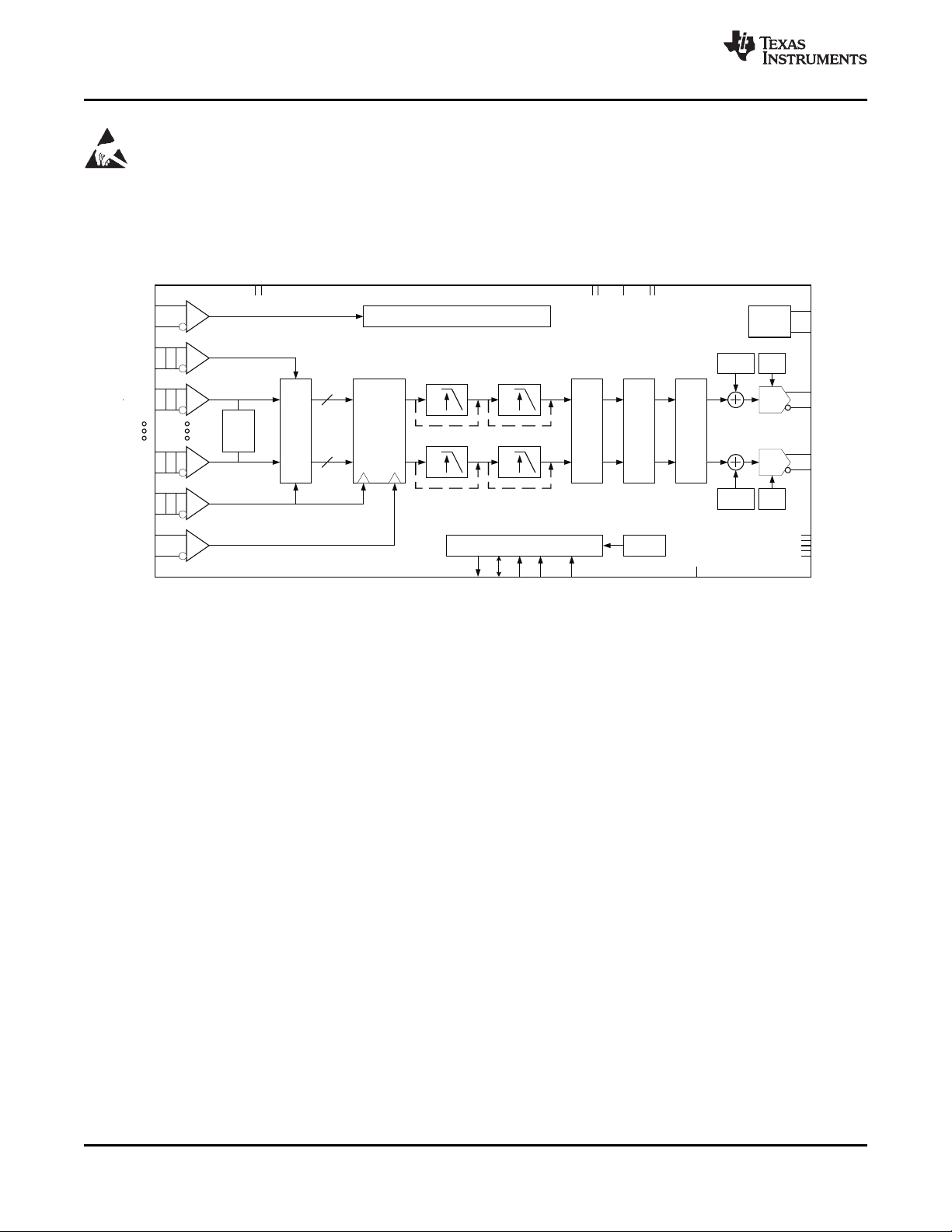
100100
Pattern
Test
De-interleave
8 Sample FIFO
16
16
100
x2
x2
Coarse Mixer
Fs/4, -Fs/4, Fs/2
QMC
Phase and Gain
1.2 V
Reference
16-b
DAC
16-b
DAC
ControlInterface
Temp
Sensor
ClockDistribution
A
gain
B
gain
FrameStrobe
EXTIO
BIASJ
IOUTA1
IOUTA2
IOUTB1
IOUTB2
DACCLKP
DACCLKN
DATACLKP
DATACLKN
D7P
D7N
D0P
D0N
FRAMEP
FRAMEN
OSTRP
OSTRN
QMC
A-offset
QMC
B-offset
ALARM_SDO
SDIO
SDENB
SCLK
TXENABLE
AVDD33
CLKVDD18
DIGVDD18
VFUSE
DACVDD18
GND
LVPECL
LVDS
LVPECL
LVDS
LVDS
FIR1FIR0
59 taps 23 taps
100
LVDS
x2
x2
Programmable Delay
(0-3T)
DAC3283
SLAS693A –MARCH 2010–REVISED APRIL 2010
This integrated circuit can be damaged by ESD. Texas Instruments recommends that all integrated circuits be handled with
appropriate precautions. Failure to observe proper handling and installation procedures can cause damage.
ESD damage can range from subtle performance degradation to complete device failure. Precision integrated circuits may be more
susceptible to damage because very small parametric changes could cause the device not to meet its published specifications.
www.ti.com
FUNCTIONAL BLOCK DIAGRAM
2 Submit Documentation Feedback Copyright © 2010, Texas Instruments Incorporated
Product Folder Link(s): DAC3283
Page 3
37
38
39
40
41
42
43
44
45
46
47
48
1
2
3
4
5
6
7
8
9
10
11
12
24
23
22
21
20
19
18
17
16
15
14
13
35
34
33
32
31
30
29
28
27
26
25
DAC3283
RGZPackage
48-QFN 7x7mm
(TopView )
36
GND
DACCLKN
D5P
D5N
D4P
D4N
DATACLKP
DATACLKN
FRAMEP
FRAMEN
D3P
D3N
D2P
D2N
D1P
D1N
D0P
D0N
TXENABLE
SDIO
SCLK
SDENB
AVDD33
AVDD33
IOUTB1
IOUTB2
VFUSE
BIASJ
EXTIO
AVDD33
IOUTA2
IOUTA1
AVDD33
AVDD33
D6N
D6P
D7N
D7P
DIGVDD18
OSTRN
OSTRP
DACCLKP
DACVDD18
CLKVDD18 DACVDD18
CLKVDD18
ALARM_SDO
DIGVDD18
DAC3283
www.ti.com
SLAS693A –MARCH 2010–REVISED APRIL 2010
DAC3283
RGZ PACKAGE
(TOP VIEW)
TERMINAL FUNCTIONS
TERMINAL
NAME NO.
AVDD33 I
37, 40, 42, Analog supply voltage. (3.3 V)
45, 48
ALARM_SDO 34 O
BIASJ 43 O Full-scale output current bias. For 20mA full-scale output current, connect a 960Ω resistor to GND.
CLKVDD18 1, 35 I
D[7..0]P 15, 21, 23, I
D[7..0]N 16, 22, 24, I D7N is most significant data bit (MSB) – pin 10
DACCLKP 3 I Positive external LVPECL clock input for DAC core with a self-bias of approximately CLKVDD18/2.
DACCLKN 4 I Complementary external LVPECL clock input for DAC core. (see the DACCLKP description)
DACVDD18 2, 36 I
Copyright © 2010, Texas Instruments Incorporated Submit Documentation Feedback 3
9, 11, 13,
25, 27
10, 12, 14,
26, 28
I/O DESCRIPTION
1.8V CMOS output for ALARM condition. The ALARM output functionality is defined through the
CONFIG6 register. Default polarity is active low, but can be changed to active high via CONFIG0
alarm_pol control bit. Optionally, it can be used as the uni-directional data output in 4-pin serial
interface mode (CONFIG 23 sif4_ena = '1').
Internal clock buffer supply voltage. (1.8 V) It is recommended to isolate this supply from DACVDD18
and DIGVDD18.
LVDS positive input data bits 0 through 7. Each positive/negative LVDS pair has an internal 100 Ω
termination resistor. Data format relative to DATACLKP/N clock is Double Data Rate (DDR) with two
data transfers per DATACKP/N clock cycle. Dual channel 16-bit data is transferred byte-wide on this
single 8-bit data bus using FRAMEP/N as a frame strobe indicator.
The order of the bus can be reversed via CONFIG19 rev bit.
LVDS negative input data bits 0 through 15. (See D[7:0]P description above)
DAC core supply voltage. (1.8 V) It is recommended to isolate this supply from CLKVDD18 and
DIGVDD18.
D7P is most significant data bit (MSB) – pin 9
D0P is least significant data bit (LSB) – pin 27
D0N is least significant data bit (LSB) – pin 28
Product Folder Link(s): DAC3283
Page 4
DAC3283
SLAS693A –MARCH 2010–REVISED APRIL 2010
www.ti.com
TERMINAL FUNCTIONS (continued)
TERMINAL
NAME NO.
DATACLKP 17 I Input data D[7:0]P/N is latched on both edges of DATACLKP/N (Double Data Rate) with two data
DATACLKN 18 I LVDS negative input data clock. (See DATACLKP description)
DIGVDD18 8, 29 I
EXTIO 44 I/O = '1'. Used as internal reference output when CONFIG25 extref_ena = '0' (default). Requires a 0.1µF
FRAMEP 19 I
FRAMEN 20 I LVDS frame indicator negative input. (See the FRAMEN description)
GND I Pin 5 and the Thermal Pad located on the bottom of the QFN package is ground for all supplies.
IOUTA1 38 O full scale current sink and the least positive voltage on the IOUTA1 pin. Similarly, a 0xFFFF data input
IOUTA2 39 O IOUTA1 described above. An input data value of 0x0000 results in a 0 mA sink and the most positive
IOUTB1 47 O B-Channel DAC current output. Refer to IOUTA1 description above.
IOUTB2 46 O B-Channel DAC complementary current output. Refer to IOUTA2 description above.
OSTRP 6 I DACCLKP/N. It is used to reset the clock dividers and for multiple DAC synchronization. If unused it
OSTRN 7 I LVPECL output strobe negative input. (See the OSTRP description)
SCLK 32 I 1.8V CMOS serial interface clock. Internal pull-down.
SDENB 33 I 1.8V CMOS active low serial data enable, always an input to the DAC3283. Internal pull-up.
SDIO 31 I/O
TXENABLE 30 I When TXENABLE is low, the digital logic section is forced to all 0, and any input data is ignored.
VFUSE 41 I
5, Thermal
Pad
I/O DESCRIPTION
LVDS positive input data clock. This positive/negative pair has an internal 100 Ω termination resistor.
transfers input per DATACLKP/N clock cycle.
Digital supply voltage. (1.8V) It is recommended to isolate this supply from CLKVDD18 and
DACVDD18.
Used as external reference input when internal reference is disabled through CONFIG25 extref_ena
decoupling capacitor to AGND when used as reference output.
LVDS frame indicator positive input. This positive/negative pair has an internal 100Ω termination
resistor. This signal is captured with the rising edge of DATACLKP/N and used to indicate the
beginning of the frame. It is also used as a reset signal by the FIFO. The FRAMEP/N signal should be
edge-aligned with D[7:0]P/N.
A-Channel DAC current output. An offset binary data pattern of 0x0000 at the DAC input results in a
results in a 0 mA current sink and the most positive voltage on the IOUTA1 pin.
A-Channel DAC complementary current output. The IOUTA2 has the opposite behavior of the
voltage on the IOUTA2 pin.
LVPECL output strobe positive input. This positive/negative pair is captured with the rising edge of
can be left floating.
1.8V CMOS serial interface data. Bi-directional in 3-pin mode (default). In 4-pin interface mode, the
SDIO pin is an input only. Internal pull-down.
1.8V CMOS active high input. TXENABLE must be high for the DATA to the DAC to be enabled.
Internal pull-down.
Digital supply voltage. (1.8V) This supply pin is also used for factory fuse programming. Connect to
DACVDD18 pins for normal operation.
4 Submit Documentation Feedback Copyright © 2010, Texas Instruments Incorporated
Product Folder Link(s): DAC3283
Page 5

DAC3283
www.ti.com
SLAS693A –MARCH 2010–REVISED APRIL 2010
ABSOLUTE MAXIMUM RATINGS
over operating free-air temperature range (unless otherwise noted)
DACDVDD18
DIGVDD18
Supply voltage range CLKVDD18
VFUSE
AVDD33
CLKVDD18 to DIGDVDD18 –0.5 to 0.5 V
DACVDD18 TO DIGVDD18 –0.5 to 0.5 V
D[7..0]P ,D[7..0]N, DATACLKP, DATACLKN, FRAMEP, FRAMEN
Terminal voltage
range
DACCLKP, DACCLKN, OSTRP, OSTRN
ALARM_SDO, SDIO, SCLK, SDENB, TXENABLE
IOUTA1/B1, IOUTA2/B2
EXTIO, BIASJ
Peak input current (any input) 20 mA
Peak total input current (all inputs) –30 mA
Operating free-air temperature range, TA: DAC3283 –40 to 85 °C
Storage temperature range –65 to 150 °C
(1) Stresses beyond those listed under absolute maximum ratings may cause permanent damage to the device. These are stress ratings
only, and functional operation of these or any other conditions beyond those indicated under recommended operating conditions is not
implied. Exposure to absolute-maximum-rated conditions for extended periods may affect device reliability.
(2) Measured with respect to GND.
(2)
(2)
(2)
(2)
(2)
(2)
(2)
(2)
(1)
VALUE UNIT
–0.5 to 2.3 V
–0.5 to 2.3 V
–0.5 to 2.3 V
–0.5 to 2.3 V
–0.5 to 4 V
(2)
–0.5 to DIGVDD18 + 0.5 V
–0.5 to CLKVDD18 + 0.5 V
(2)
–0.5 to DIGCLKVDD18 + 0.5 V
–1.0 to AVDD33 + 0.5 V
–0.5 to AVDD33 + 0.5 V
THERMAL CHARACTERISTICS
over operating free-air temperature range (unless otherwise noted)
THERMAL CONDUCTIVITY 48ld QFN UNIT
T
Maximum junction temperature
J
Theta junction-to-ambient (still air) 30
q
JA
Theta junction-to-ambient (150 lfm) 24
q
Theta junction-to-board 8 °C/W
JB
q
Theta junction-to-pad 1.3 °C/W
Jp
(1) Air flow or heat sinking reduces qJAand may be required for sustained operation at 85° under maximum operating conditions.
(2) It is strongly recommended to solder the device thermal pad to the board ground plane.
(1) (2)
125 °C
°C/W
Copyright © 2010, Texas Instruments Incorporated Submit Documentation Feedback 5
Product Folder Link(s): DAC3283
Page 6
DAC3283
SLAS693A –MARCH 2010–REVISED APRIL 2010
ELECTRICAL CHARACTERISTICS — DC SPECIFICATIONS
(1)
www.ti.com
over operating free-air temperature range, nominal supplies, IOUTFS = 20 mA (unless otherwise noted)
PARAMETER TEST CONDITIONS MIN TYP MAX UNIT
RESOLUTION 16 Bits
DC ACCURACY
DNL Differential nonlinearity ±2
INL Integral nonlinearity ±4
1 LSB = IOUTFS/2
ANALOG OUTPUT
Coarse gain linearity ±0.04 LSB
Offset error Mid code offset ±0.01 %FSR
Gain error
With external reference ±2 %FSR
With internal reference ±2 %FSR
Gain mismatch With internal reference –2 2 %FSR
Minimum full scale output current 2 mA
Maximum full scale output current 20 mA
Output compliance range
(2)
Nominal full-scale current, IOUTFS = 16 x IBIAS
current.
IOUTFS = 20 mA AVDD –0.5V AVDD +0.5V V
Output resistance 300 kΩ
Output capacitance 5 pF
REFERENCE OUTPUT
V
ref
Reference output voltage 1.14 1.2 1.26 V
Reference output current
(3)
REFERENCE INPUT
V
EXTIO
Input voltage range 0.1 1.2 1.25 V
Input resistance 1 MΩ
External reference mode
Small signal bandwidth 472 kHz
Input capacitance 100 pF
TEMPERATURE COEFFICIENTS
Offset drift With external reference ±1
Gain drift With internal reference
Reference voltage drift ±8 ppm/°C
POWER SUPPLY
AVDD33 3.0 3.3 3.6 V
DACVDD18, DIGVDD18, CLKVDD18 1.7 1.8 1.9 V
I
(AVDD33)
I
(DIGDVDD)
I
(DACVDD18)
I
(CLKVDD18)
Analog supply current 149 mA
Digital supply current 340 mA
DAC supply current 55 mA
Mode 1 (below)
Clock supply current 37 mA
Mode 1: f
4x interpolation, Fs/4 mixer on, QMC on
Mode 2: f
2x interpolation, Mixer off, QMC on
P Power dissipation
Mode 3: Sleep mode
f
= 800MSPS, 4x interpolation, Fs/4 mixer on, 750 mW
DAC
CONFIG24 sleepa, sleepb set = 1
Mode 4: Power-Down mode
No clock, static data pattern,
CONFIG23 clkpath_sleep_a, clkpath_sleepb set = 1
CONFIG24 clkrecv_sleep, sleepa, sleepb set = 1
PSRR Power supply rejection ratio DC tested ±0.2 %FSR/V
T Operating range –40 25 85 °C
(1) Measured differential across IOUTA1 and IOUTA2 with 25 Ω each to AVDD.
(2) The lower limit of the output compliance is determined by the CMOS process. Exceeding this limit may result in transistor breakdown,
resulting in reduced reliability of the DAC3283 device. The upper limit of the output compliance is determined by the load resistors and
full-scale output current. Exceeding the upper limit adversely affects distortion performance and integral nonlinearity.
(3) Use an external buffer amplifier with high impedance input to drive any external load.
= 800MSPS,
DAC
= 491.52MSPS,
DAC
16
LSB
100 nA
ppm of
FSR/°C
±15
±30
ppm of
FSR/°C
1300 1450 mW
1000 mW
7 18 mW
6 Submit Documentation Feedback Copyright © 2010, Texas Instruments Incorporated
Product Folder Link(s): DAC3283
Page 7

DAC3283
www.ti.com
SLAS693A –MARCH 2010–REVISED APRIL 2010
ELECTRICAL CHARACTERISTICS — AC SPECIFICATIONS
Over recommended operating free-air temperature range, nominal supplies, IOUTFS = 20 mA (unless otherwise noted)
PARAMETER TEST CONDITIONS MIN TYP MAX UNIT
ANALOG OUTPUT
f
DAC
t
s(DAC)
t
pd
t
r(IOUT)
t
f(IOUT)
Power-up
time
AC PERFORMANCE
SFDR f
IMD3 f
NSD dBc/Hz
WCDMA
(3)
(1) Measured single-ended into 50Ω load.
(2) 4:1 transformer output termination, 50Ω doubly terminated load
(3) Single carrier, W-CDMA with 3.84 MHz BW, 5-MHz spacing, centered at f
(1)
1x Interpolation 312.5
Maximum DAC output update rate 2x Interpolation 625 MSPS
4x Interpolation 800
Output settling time to 0.1% Transition: Code 0x0000 to 0xFFFF 10.4 ns
Output propagation delay DAC outputs are updated on the falling edge of DAC 2
clock. Does not include digital latency (see below).
ns
Output rise time 10% to 90% 220 ps
Output fall time 90% to 10% 220 ps
IOUT current settling to 1% of IOUTFS. Measured
DAC wake-up time from SDENB rising edge; Register CONFIG24, 90
toggle sleepa from 1 to 0.
IOUT current settling to less than 1% of IOUTFS.
µs
DAC sleep time Measured from SDENB rising edge; Register 90
CONFIG24, toggle sleepa from 0 to 1.
1x Interpolation 59
Digital latency clock
2x Interpolation 139
4x Interpolation 290
DAC
cycles
QMC 24
(2)
f
Spurious free dynamic range (0 to
f
/2)Tone at 0 dBFS
DAC
Third-order two-tone
intermodulation distortion
Each tone at –12 dBFS
Noise spectral density tone at
0dBFS
Adjacent channel leakage ratio,
single carrier
Alternate channel leakage ratio,
single carrier
Channel isolation f
= 800 MSPS, f
DAC
= 800 MSPS, f
DAC
f
= 800 MSPS, f
DAC
f
= 800 MSPS, f
DAC
= 800 MSPS, f
DAC
f
= 800 MSPS, f
DAC
f
= 800 MSPS, f
DAC
f
= 800 MSPS, f
DAC
f
= 737.28 MSPS, f
DAC
f
= 737.28 MSPS, f
DAC
f
= 737.28 MSPS, f
DAC
f
= 737.28 MSPS, f
DAC
= 800 MSPS, f
DAC
= 20.1 MHz 85
OUT
= 50.1 MHz 76 dBc
OUT
= 70.1 MHz 72
OUT
= 30 ± 0.5 MHz 93
OUT
= 50 ± 0.5 MHz 90 dBc
OUT
= 100 ± 0.5 MHz 86
OUT
= 10.1 MHz 162
OUT
= 80.1 MHz 160
OUT
= 30.72MHz 85
OUT
= 153.6MHz 81
OUT
= 30.72MHz 91
OUT
= 153.6MHz 85
OUT
= 10MHz 84 dBc
OUT
, PAR = 12dB. TESTMODEL 1, 10 ms
OUT
dBc
dBc
Copyright © 2010, Texas Instruments Incorporated Submit Documentation Feedback 7
Product Folder Link(s): DAC3283
Page 8
DAC3283
SLAS693A –MARCH 2010–REVISED APRIL 2010
www.ti.com
ELECTRICAL CHARACTERISTICS – DIGITAL SPECIFICATIONS
over recommended operating free-air temperature range, nominal supplies, IOUTFS = 20 mA (unless otherwise noted)
PARAMETER TEST CONDITIONS MIN TYP MAX UNIT
LVDS INTERFACE:D[7:0]P/N, DATACLKP/N, FRAMEP/N
f
DATA
f
BUS
V
V
V
Z
C
A,B+
A,B–
COM
T
L
Input data rate 312.5 MSPS
Byte-wide LVDS data transfer rate 1250 MSPS
Logic high differential input voltage threshold 150 400 mV
Logic low differential input voltage threshold –150 –400 mV
Input common mode 0.9 1.2 1.5 V
Internal termination 85 110 135 Ω
LVDS Input capacitance 2 pF
TIMING LVDS INPUTS: DATACLKP/N DOUBLE EDGE LATCHING – See Figure 40
t
s(DATA)
t
h(DATA)
t
(FRAME)
t
_align
Setup time, D[7:0]P/N and FRAMEP/N, valid FRAMEP/N latched on rising edge of
to either edge of DATACLKP/N DATACLKP/N only
Hold time, D[7:0]P/N and FRAMEP/N, valid FRAMEP/N latched on rising edge of
after either edge of DATACLKP/N DATACLKP/N only
FRAMEP/N pulse width f
Maximum offset between DATACLKP/N and FIFO bypass mode only f
DACCLKP/N rising edges DACCLK frequency in MHz –0.55
CLOCK INPUT (DACCLKP/N)
Duty cycle 40% 60%
Differential voltage
(2)
DACCLKP/N Input Frequency 800 MHz
OUTPUT STROBE (OSTRP/N)
f
OSTR
Frequency any positive integer f
Duty cycle 40% 60%
Differential voltage 0.4 1.0 V
TIMING OSTRP/N INPUT: DACCLKP/N RISING EDGE LATCHING
t
s(OSTR)
t
h(OSTR)
Setup time, OSTRP/N valid to rising edge of
DACCLKP/N
Hold time, OSTRP/N valid after rising edge
of DACCLKP/N
CMOS INTERFACE: ALARM_SDO, SDIO, SCLK, SDENB, TXENABLE
V
IH
V
IL
I
IH
I
IL
High-level input voltage 1.25 V
Low-level input voltage 0.54 V
High-level input current –40 40 mA
Low-level input current –40 40 mA
CI CMOS input capacitance 2 pF
V
OH
V
OL
ALARM_SDO, SDIO
ALARM_SDO, SDIO
SERIAL PORT TIMING – See Figure 32 and Figure 33
t
s(SDENB)
t
s(SDIO)
t
h(SDIO)
t
(SCLK)
Setup time, SDENB to rising edge of SCLK 20 ns
Setup time, SDIO valid to rising edge of
SCLK
Hold time, SDIO valid to rising edge of SCLK 5 ns
Period of SCLK
(1)
Byte-wide DDR format
DATACLK frequency = 625 MHz
–25 ps
375 ps
is DATACLK frequency in MHz 1/2f
DATACLK
is 1/2f
DACCLK
DATACLK
DACCLK
0.4 1.0 V
f
= f
OSTR
frequency in MHz
/ (n × 8 × Interp) where n is
DACCLK
DACCLK
is DACCLK
f
DACCLK
x interp)
/ (8
200 ps
200 ps
I
= –100 mA V
load
I
= –2mA V
load
I
= 100 mA 0.2 V
load
I
= 2 mA 0.5 V
load
DIGVDD18
–0.2
0.8 x
DIGVDD18
10 ns
Register CONFIG5 read (temperature
sensor read)
1 ms
All other registers 100 ns
ns
ns
(1) See LVDS INPUTS section for terminology.
(2) Driving the clock input with a differential voltage lower than 1V will result in degraded performance.
8 Submit Documentation Feedback Copyright © 2010, Texas Instruments Incorporated
Product Folder Link(s): DAC3283
Page 9
DAC3283
www.ti.com
SLAS693A –MARCH 2010–REVISED APRIL 2010
ELECTRICAL CHARACTERISTICS – DIGITAL SPECIFICATIONS (continued)
over recommended operating free-air temperature range, nominal supplies, IOUTFS = 20 mA (unless otherwise noted)
PARAMETER TEST CONDITIONS MIN TYP MAX UNIT
t
(SCLKH)
t
(SCLKL)
t
d(Data)
Register CONFIG5 read (temperature
High time of SCLK
Low time of SCLK
Data output delay after falling edge of SCLK 10 ns
sensor read)
All other registers 40 ns
Register CONFIG5 read (temperature
sensor read)
All other registers 40 ns
0.4 ms
0.4 ms
Copyright © 2010, Texas Instruments Incorporated Submit Documentation Feedback 9
Product Folder Link(s): DAC3283
Page 10
-5
-4
-3
-2
-1
0
1
2
3
4
5
Error-LSB
0 10000 20000 30000 40000 50000 60000 70000
Code
0 10000 20000 30000 40000 50000 60000 70000
Code
-5
-4
-3
-2
-1
0
1
2
3
4
5
Error-LSB
50
55
60
65
70
75
80
85
90
95
100
0 50 100 150 200 250 300 350
f -MHz
OUT
0dBFS
-6dBFS
-12dBFS
f = 800 MSPS, 4x Interpolation,
IOUTFS = 20 mA
DAC
SecondHarmonic-dBc
0dBFS
-6dBFS
-12dBFS
f = 800 MSPS,4x Interpolation,
IOUTFS = 20 mA
DAC
50
55
60
65
70
75
80
85
90
95
100
SFDR-SpuriousFreeDynamicRange-dBc
0 50 100 150 200 250 300 350
f -MHz
OUT
DAC3283
SLAS693A –MARCH 2010–REVISED APRIL 2010
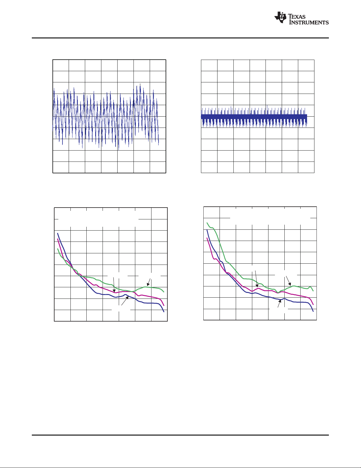
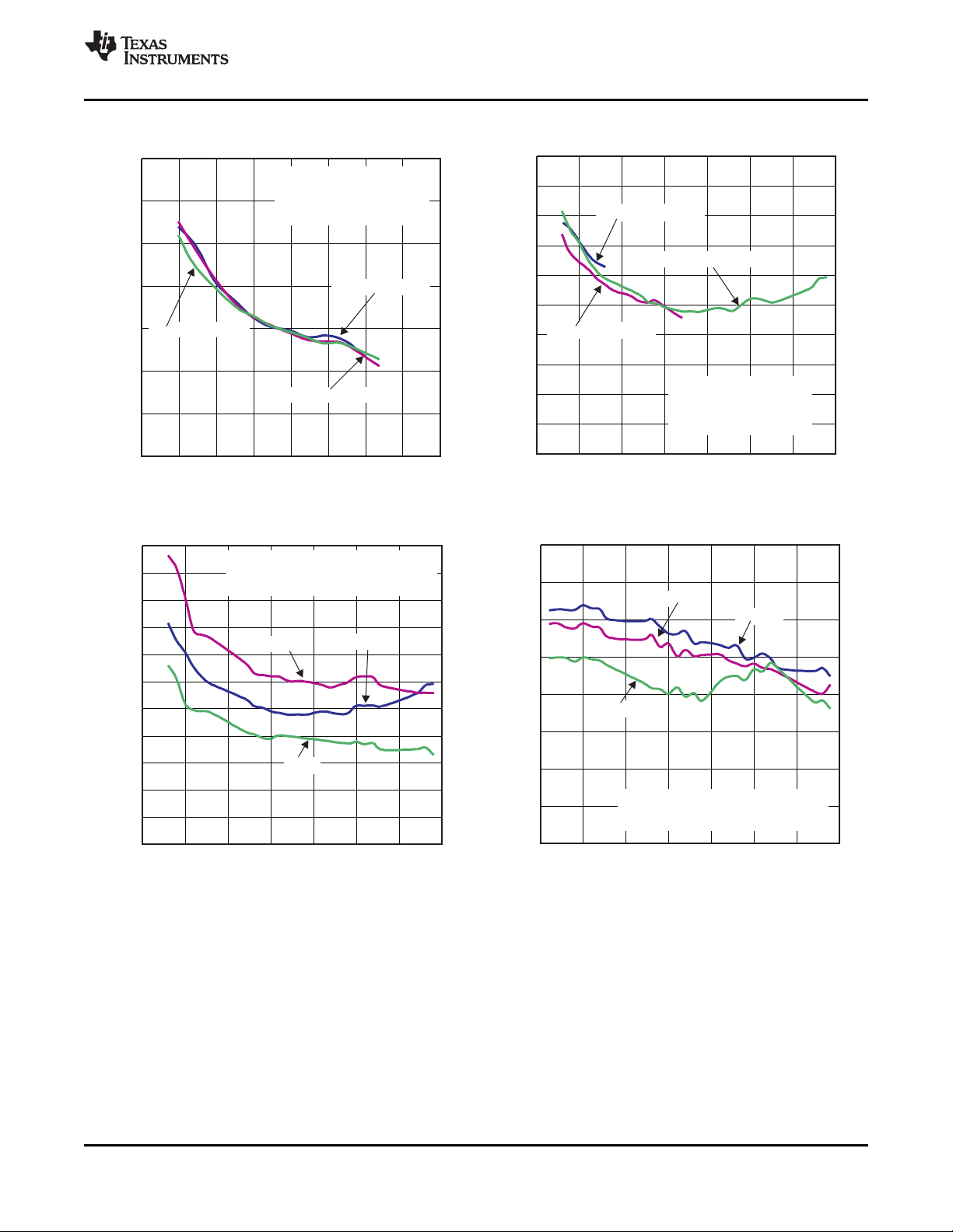
Figure 1. INTEGRAL NON-LINEARITY Figure 2. DIFFERENTIAL NON-LINEARITY
www.ti.com
TYPICAL CHARACTERISTICS
Figure 3. SPURIOUS FREE DYNAMIC RANGE vs INPUT SCALE Figure 4. SECOND HARMONIC vs INPUT SCALE
10 Submit Documentation Feedback Copyright © 2010, Texas Instruments Incorporated
Product Folder Link(s): DAC3283
Page 11
0 20 40 60 80 100 120
1xinterpolation
2xinterpolation
4xinterpolation
f -MHz
OUT
50
55
60
65
70
75
80
85
90
95
100
SFDR-SpuriousFreeDynamicRange-dBc
f = 312.5 MSPS, 0 dBFS,
IOUTFS = 20 mA
DAC
50
55
60
65
70
75
80
85
90
95
100
105
0 50 100 150 200 250 300 350
f -MHz
OUT
0dBFS
-6dBFS
-12dBFS
ThirdHarmonic-dBc
f = 800 MSPS, 4x Interpolation,
IOUTFS = 20 mA
DAC
20mA
10mA
2mA
50
55
60
65
70
75
80
85
90
95
100
SFDR-SpuriousFreeDynamicRange-dBc
0 50 100 150 200 250 300 350
f -MHz
OUT
f = 800 MSPS,4x Interpolation,
0 dBFS
DAC
f =200MSPS
DAC
f =400MSPS
DAC
f =800MSPS
DAC
50
55
60
65
70
75
80
85
90
95
100
SFDR-SpuriousFreeDynamicRange-dBc
0 50 100 150 200 250 300 350
f -MHz
OUT
4x Interpolation, 0 dBFS
IOUTFS = 20 mA
DAC3283
www.ti.com
SLAS693A –MARCH 2010–REVISED APRIL 2010
TYPICAL CHARACTERISTICS (continued)
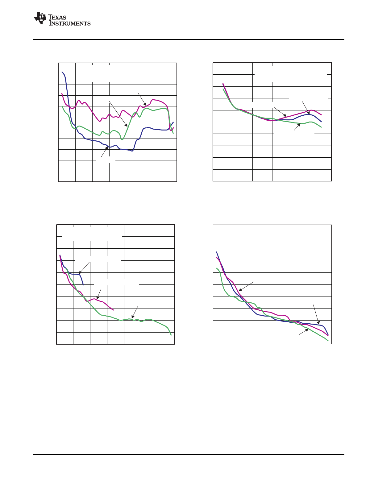
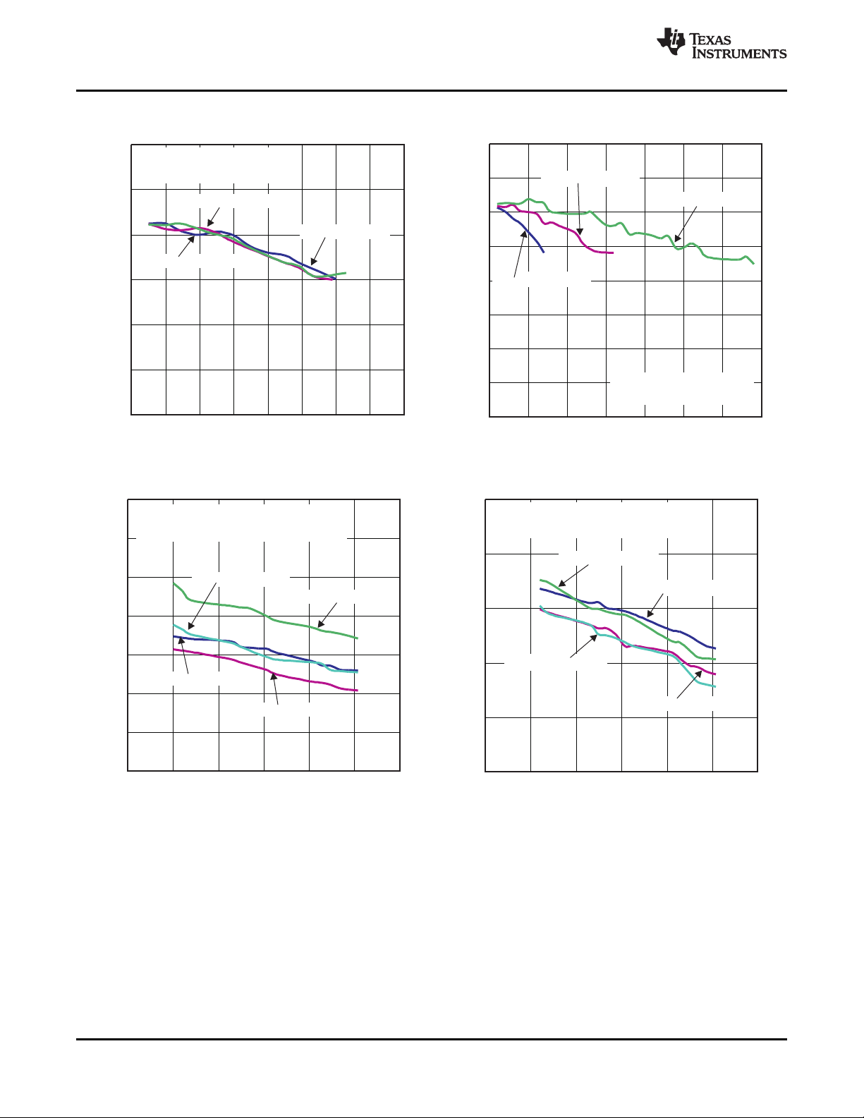
Figure 5. THIRD HARMONIC vs INPUT SCALE Figure 6. SPURIOUS FREE DYNAMIC RANGE vs
INTERPOLATION
Figure 7. SPURIOUS FREE DYNAMIC RANGE vs f
Copyright © 2010, Texas Instruments Incorporated Submit Documentation Feedback 11
DAC
Figure 8. SPURIOUS FREE DYNAMIC RANGE vs IOUTFS
Product Folder Link(s): DAC3283
Page 12

-90
-80
-70
-60
-50
-40
-30
-20
-10
0
10
Power-dBm
10 60 110 160 210
f-Frequency-MHz
2xInterpolation,
f =500MSPS,
f =50MHz
DAC
OUT
-90
-80
-70
-60
-50
-40
-30
-20
-10
0
10
Power-dBm
10 60 110 160 210
f-Frequency-MHz
2xInterpolation,
f =500MSPS,
f =100MHz
DAC
OUT
50
55
60
65
70
75
80
85
90
95
100
IMD3-dBc
0 50 100 150 200 250 300 350
f -MHz
OUT
0dBFS
-6dBFS
-12dBFS
f = 800 MSPS, 4x Interpolation,
Tonesat f ±0.5 MHz,
IOUTFS = 20 mA
DAC
OUT
10 60 110 160 210 260 310 360
-90
-80
-70
-60
-50
-40
-30
-20
-10
0
10
Power-dBm
f-Frequency-MHz
4xInterpolation,0dBFS
f =800MSPS,
f =150MHz
DAC
OUT
DAC3283
SLAS693A –MARCH 2010–REVISED APRIL 2010
TYPICAL CHARACTERISTICS (continued)
Figure 9. SINGLE TONE SPECTRAL PLOT Figure 10. SINGLE TONE SPECTRAL PLOT
www.ti.com
12 Submit Documentation Feedback Copyright © 2010, Texas Instruments Incorporated
Figure 11. SINGLE TONE SPECTRAL PLOT Figure 12. IMD3 vs INPUT SCALE
Product Folder Link(s): DAC3283
Page 13
65
70
75
80
85
90
95
100
0 20 40 60 80 100 120 140 160
1xinterpolation
2xinterpolation
4xinterpolation
IMD3-dBc
f -MHz
OUT
f = 312.5 MSPS,
Tonesat f ±0.5 MHz,
0 dBFS, IOUTFS = 20 mA
DAC
OUT
f =200MSPS
DAC
f =400MSPS
DAC
f =800MSPS
DAC
50
55
60
65
70
75
80
85
90
95
100
IMD3-dBc
0 50 100 150 200 250 300 350
f -MHz
OUT
4x Interpolation,
Tonesat f ±0.5 MHz,
0 dBFS, IOUTFS = 20 mA
OUT
130
135
140
145
150
155
160
165
170
0 50 100 150 200 250 300 350
f -MHz
OUT
NSD-dBc/Hz
0dBFS
-6dBFS
-12dBFS
f = 800 MSPS, 4x Interpolation,
IOUTFS = 20 mA
DAC
50
55
60
65
70
75
80
85
90
95
100
105
20mA
10mA
2mA
0 50 100 150 200 250 300 350
f -MHz
OUT
IMD3-dBc
f = 800 MSPS, 4x Interpolation,
Tonesat f ±0.5 Mhz, 0 dBFS
DAC
OUT
DAC3283
www.ti.com
SLAS693A –MARCH 2010–REVISED APRIL 2010
TYPICAL CHARACTERISTICS (continued)
Figure 13. IMD3 vs INTERPOLATION Figure 14. IMD3 vs f
DAC
Copyright © 2010, Texas Instruments Incorporated Submit Documentation Feedback 13
Figure 15. IMD3 vs IOUTFS Figure 16. NSD vs INPUT SCALE
Product Folder Link(s): DAC3283
Page 14
140
145
150
155
160
165
170
0 20 40 60 80 100 120 140 160
f -MHz
OUT
1xinterpolation
2xinterpolation
4xinterpolation
NSD-dBc/Hz
f = 312.5 MSPS, 0 dBFS,
IOUTFS = 20 mA
DAC
130
135
140
145
150
155
160
165
170
f =200MSPS
DAC
f =400MSPS
DAC
f =800MSPS
DAC
0 50 100 150 200 250 300 350
f -MHz
OUT
NSD-dBc/Hz
4x interpolation, 0 dBFS,
IOUTFS = 20 mA
60
65
70
75
80
85
0 50 100 150 200 250 300
ACLR,0dBFS
ACLR-6dBFS
Aternate,0dBFS
Alternate,-6dBFS
f -MHz
OUT
ACLR-dBc
f = 737.28 MSPS, 4x Interpolation,
IOUTFS = 20 mA
DAC
65
70
75
80
85
90
95
100
0 50 100 150 200 250 300
Adjacent0dBFS
Adjacent-6dBFS
Alternate0dBFS
Alternate-6dBFS
f -MHz
OUT
ACLR-dBc
f = 737.28 MSPS, 4x Interpolation,
IOUTFS = 20 mA
DAC
DAC3283
SLAS693A –MARCH 2010–REVISED APRIL 2010
TYPICAL CHARACTERISTICS (continued)
Figure 17. NSD vs INTERPOLATION Figure 18. NSD vs f
www.ti.com
DAC
Figure 19. SINGLE CARRIER WCDMA ACLR vs INPUT SCALE Figure 20. FOUR CARRIER WCDMA ACLR vs INPUT SCALE
14 Submit Documentation Feedback Copyright © 2010, Texas Instruments Incorporated
Product Folder Link(s): DAC3283
Page 15
A
Re f -1 2 .3 d Bm
*
*
*
CL RW R
RB W 3 0 k Hz
VB W 3 0 0 kH z
SW T 1 0 sAt t 1 0 d B*
1 R M
NO R
*
Ce nt er 7 0 MH z Spa n 2 5. 5 M Hz2. 55 MH z/
-1 20
-1 10
-1 00
-9 0
-8 0
-7 0
-6 0
-5 0
-4 0
-3 0
-2 0
Tx C h an n e l W -C D M A 3G P P FW D
Ba n d wi d th 3 .8 4 M Hz
P o w e r - 7 . 7 1 d B m
Ad j a ce n t Ch a nn e l
Ba n d wi d th 3 .8 4 M Hz
L o w e r - 8 2 . 2 0 d B
Sp a c in g 5 MH z
U p p e r - 8 2 . 0 7 d B
Al t e rn a te C h an n e l
Ba n d wi d th 3 .8 4 M Hz
L o w e r - 8 6 . 1 1 d B
Sp a c in g 10 MH z
U p p e r - 8 5 . 8 6 d B
4xInterpolation,0dBFS
f =737.28MSPS,
f =70MHz
DAC
OUT
A
Re f -1 2 .8 d Bm
*
*
*
CL RW R
RB W 30 k Hz
VB W 30 0 kH z
SW T 10 sAt t 1 0 d B*
1 R M
NO R
*
Ce nt er 1 53 .6 MH z Sp an 2 5 .5 M Hz2. 55 MH z/
-1 20
-1 10
-1 00
-9 0
-8 0
-7 0
-6 0
-5 0
-4 0
-3 0
-2 0
Tx C h an n e l W - CD M A 3G P P FW D
Ba n d wi d th 3 .8 4 M Hz
P o w e r - 8 . 0 7 d B m
Ad j a ce n t Ch a nn e l
Ba n d wi d th 3 .8 4 M Hz
L o w e r - 8 0 . 6 9 d B
Sp a c in g 5 MH z
U p p e r - 8 1 . 0 0 d B
Al t e rn a te C h an n e l
Ba n d wi d th 3 .8 4 M Hz
L o w e r - 8 4 . 0 7 d B
Sp a c in g 10 MH z
U p p e r - 8 4 . 1 6 d B
4xInterpolation,0dBFS
f =737.28MSPS,
f =153.6MHz
DAC
OUT
A
Re f -1 7. 9 d Bm
*
*
*
CL RW R
RB W 3 0 k Hz
VB W 3 00 kH z
SW T 1 0 sAt t 10 dB*
1 RM
NO R
*
Ce nt er 1 53 .6 M Hz Sp an 3 5 M Hz3. 5 M Hz /
-1 20
-1 10
-1 00
-9 0
-8 0
-7 0
-6 0
-5 0
-4 0
-3 0
-2 0
Tx C h an n e l W - CD M A 3G P P FW D
Ba n d wi d th 1 0 M Hz
P o w e r - 8 . 8 9 d B m
Ad j a ce n t Ch a nn e l
Ba n d wi d th 1 0 M Hz
L o w e r - 7 8 . 2 1 d B
Sp a c in g 1 0. 5 M Hz
U p p e r - 7 8 . 1 2 d B
4xInterpolation,0dBFS
f =737.28MSPS,
f =153.6MHz
DAC
OUT
A
Re f -1 7 .4 d Bm
*
*
*
CL RW R
RB W 3 0 k Hz
VB W 3 0 0 kH z
SW T 1 0 sAt t 1 0 dB*
1 R M
NO R
*
Ce nt er 7 0 MH z Sp an 3 5 M Hz3. 5 M Hz /
-1 20
-1 10
-1 00
-9 0
-8 0
-7 0
-6 0
-5 0
-4 0
-3 0
-2 0
Tx C h an n e l W - CD M A 3G P P F WD
Ba n d wi d th 1 0 M H z
P o w e r - 8 . 5 0 d B m
Ad j a ce n t Ch a nn e l
Ba n d wi d th 1 0 M H z
L o w e r - 7 9 . 6 4 d B
Sp a c in g 1 0. 5 M H z
U p p e r - 8 0 . 0 5 d B
4xInterpolation,0dBFS
f =737.28MSPS,
f =70MHz
DAC
OUT
A
Re f -1 9 d Bm
*
*
*
CL RW R
RB W 3 0 k Hz
VB W 3 0 0 kH z
SW T 1 0 sAtt 1 0 dB*
1 R M
NO R
*
Ce nt er 7 0 MH z Sp a n 65 MH z6. 5 M Hz /
-1 20
-1 10
-1 00
-9 0
-8 0
-7 0
-6 0
-5 0
-4 0
-3 0
Tx C h an n e l W - CD M A 3G P P F WD
Ba n dw i d th 2 0 M H z
P o w e r - 7 . 3 8 d B m
Ad j ac e n t C h a nn e l
Ba n dw i d th 2 0 M H z
L o w e r - 7 7 . 2 8 d B
Sp a ci n g 2 0. 5 M H z
U p p e r - 7 7 . 0 7 d B
4xInterpolation,0dBFS
f =737.28MSPS,
f =70MHz
DAC
OUT
A
Re f -1 9. 6 d Bm
*
*
*
CL RW R
RB W 3 0 k Hz
VB W 3 00 kH z
SW T 1 0 sAt t 1 0 dB*
1 RM
NO R
*
Ce nt er 1 53 .6 M Hz Sp an 6 5 M Hz6. 5 M Hz /
-1 20
-1 10
-1 00
-9 0
-8 0
-7 0
-6 0
-5 0
-4 0
-3 0
Tx C h an n e l W -C D MA 3 G P P F W D
Ba n dw i d th 2 0 M Hz
P o w e r - 8 . 0 2 d B m
Ad j ac e n t Ch a nn e l
Ba n dw i d th 2 0 M Hz
L o w e r - 7 3 . 4 1 d B
Sp a ci n g 2 0. 5 M Hz
U p p e r - 7 3 . 5 4 d B
2xInterpolation,0dBFS
f =492.52MSPS,
f =153.6MHz
DAC
OUT
DAC3283
www.ti.com
SLAS693A –MARCH 2010–REVISED APRIL 2010
TYPICAL CHARACTERISTICS (continued)
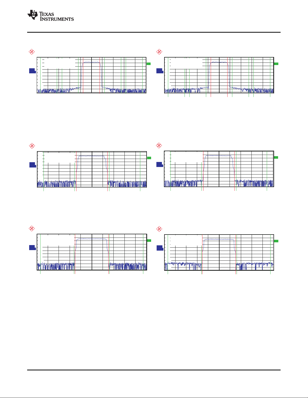
Figure 21. SINGLE CARRIER W-CDMA TEST MODEL 1 Figure 22. SINGLE CARRIER W-CDMA TEST MODEL 1
Figure 23. 10MHZ SINGLE CARRIER LTE Figure 24. 10MHZ SINGLE CARRIER LTE
Figure 25. 20MHZ SINGLE CARRIER LTE Figure 26. 20MHZ SINGLE CARRIER LTE
Copyright © 2010, Texas Instruments Incorporated Submit Documentation Feedback 15
Product Folder Link(s): DAC3283
Page 16
2x
1x
4x
QMC
Mixer
0
200
400
600
800
1000
1200
f -MSPS
DAC
0 100 200 300 400 500 600 700 800 900
Power-mW
0
50
100
150
200
250
300
350
2x
0 100 200 300 400 500 600 700 800 900
DVDD18-mA
f -MSPS
DAC
1x
4x
QMC
Mixer
0
10
20
30
40
50
60
70
80
0 100 200 300 400 500 600 700 800 900
DACVDD18-mA
f -MSPS
DAC
MixerOn
MixerOff
0
5
10
15
20
25
30
35
40
0 100 200 300 400 500 600 700 800 900
CLKVDD18-mA
f -MSPS
DAC
DAC3283
SLAS693A –MARCH 2010–REVISED APRIL 2010
TYPICAL CHARACTERISTICS (continued)
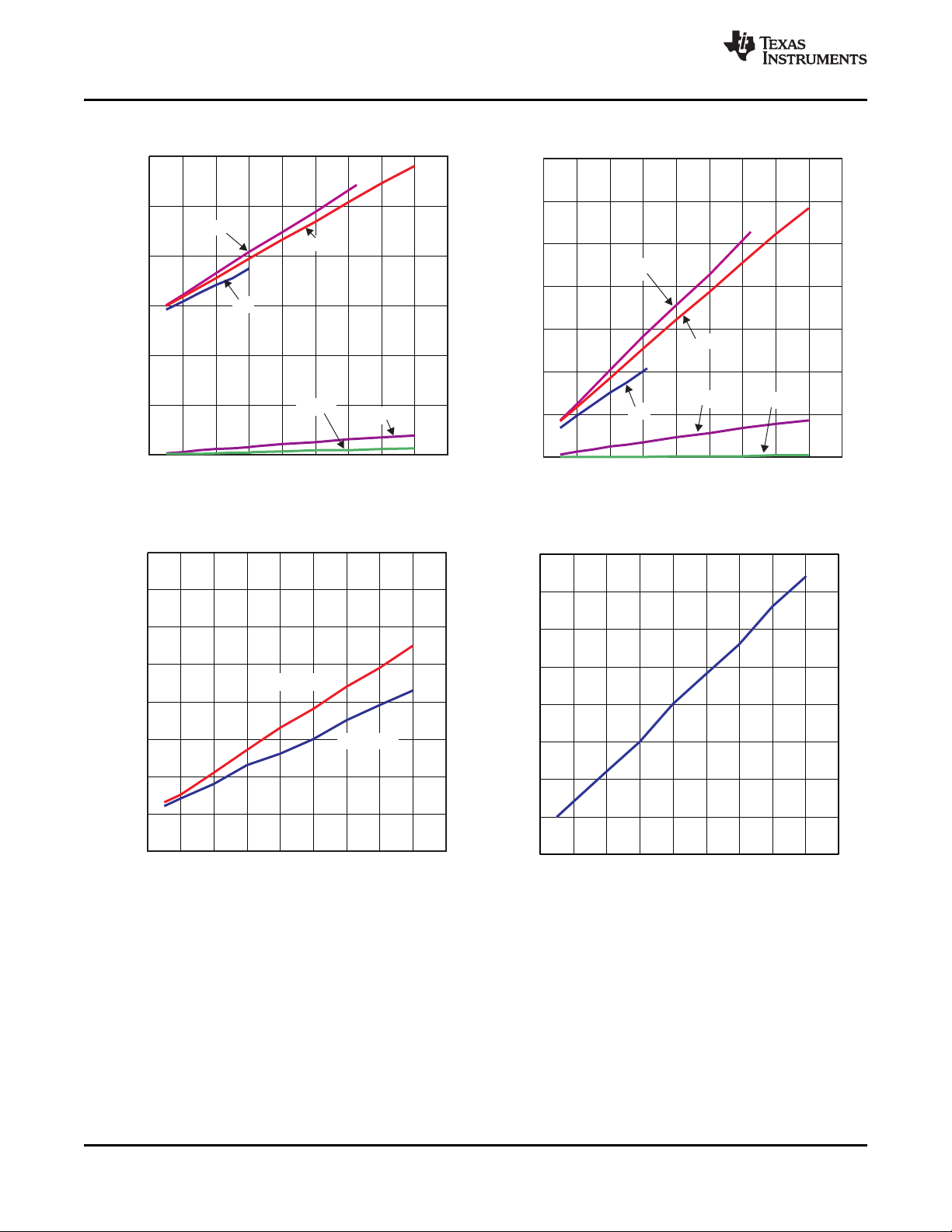
Figure 27. POWER vs f
DAC
Figure 28. DVDD18 vs f
www.ti.com
DAC
16 Submit Documentation Feedback Copyright © 2010, Texas Instruments Incorporated
Figure 29. DACVDD18 vs f
DAC
Product Folder Link(s): DAC3283
Figure 30. CLKVDD18 vs f
DAC
Page 17

0
20
40
60
80
100
120
140
160
180
200
0 100 200 300 400 500 600 700 800 900
AVDD33-mA
f -MSPS
DAC
DAC3283
www.ti.com
SLAS693A –MARCH 2010–REVISED APRIL 2010
TYPICAL CHARACTERISTICS (continued)
Figure 31. AVDD33 vs f
DAC
Copyright © 2010, Texas Instruments Incorporated Submit Documentation Feedback 17
Product Folder Link(s): DAC3283
Page 18

DAC3283
SLAS693A –MARCH 2010–REVISED APRIL 2010
www.ti.com
FUNCTIONAL DESCRIPTION
DEFINITION OF SPECIFICATIONS
Adjacent Carrier Leakage Ratio (ACLR): Defined for a 3.84Mcps 3GPP W-CDMA input signal measured in a
3.84MHz bandwidth at a 5MHz offset from the carrier with a 12dB peak-to-average ratio.
Analog and Digital Power Supply Rejection Ratio (APSSR, DPSSR): Defined as the percentage error in the
ratio of the delta IOUT and delta supply voltage normalized with respect to the ideal IOUT current.
Differential Nonlinearity (DNL): Defined as the variation in analog output associated with an ideal 1 LSB
change in the digital input code.
Gain Drift: Defined as the maximum change in gain, in terms of ppm of full-scale range (FSR) per °C, from the
value at ambient (25°C) to values over the full operating temperature range.
Gain Error: Defined as the percentage error (in FSR%) for the ratio between the measured full-scale output
current and the ideal full-scale output current.
Integral Nonlinearity (INL): Defined as the maximum deviation of the actual analog output from the ideal output,
determined by a straight line drawn from zero scale to full scale.
Intermodulation Distortion (IMD3, IMD): The two-tone IMD3 or four-tone IMD is defined as the ratio (in dBc) of
the worst 3rd-order (or higher) intermodulation distortion product to either fundamental output tone.
Offset Drift: Defined as the maximum change in DC offset, in terms of ppm of full-scale range (FSR) per °C,
from the value at ambient (25°C) to values over the full operating temperature range.
Offset Error: Defined as the percentage error (in FSR%) for the ratio between the measured mid-scale output
current and the ideal mid-scale output current.
Output Compliance Range: Defined as the minimum and maximum allowable voltage at the output of the
current-output DAC. Exceeding this limit may result reduced reliability of the device or adversely affecting
distortion performance.
Reference Voltage Drift: Defined as the maximum change of the reference voltage in ppm per degree Celsius
from value at ambient (25°C) to values over the full operating temperature range.
Spurious Free Dynamic Range (SFDR): Defined as the difference (in dBc) between the peak amplitude of the
output signal and the peak spurious signal.
Signal to Noise Ratio (SNR): Defined as the ratio of the RMS value of the fundamental output signal to the
RMS sum of all other spectral components below the Nyquist frequency, including noise, but excluding the first
six harmonics and dc.
18 Submit Documentation Feedback Copyright © 2010, Texas Instruments Incorporated
Product Folder Link(s): DAC3283
Page 19

DAC3283
www.ti.com
SLAS693A –MARCH 2010–REVISED APRIL 2010
REGISTER DESCRIPTIONS
Table 1. Register Map
Name Address Default Bit 6 Bit 5 Bit 4 Bit 3 Bit 2 Bit 1
CONFIG0 0x00 0x70 reserved fifo_ena fifo_reset_ena multi_sync_ena alarm_out_ena alarm_pol mixer_func(1:0)
CONFIG1 0x01 0x11 qmc_offset_ena qmc_correct_ena fir0_ena fir1_ena unused iotest_ena unused twos
CONFIG2 0x02 0x00 unused unused sif_sync sif_sync_ena unused unused output_delay(1:0)
CONFIG3 0x03 0x10 64cnt_ena unused unused fifo_offset(2:0) alarm_ 1away_ena
CONFIG4 0x04 0xFF coarse_daca(3:0) coarse_dacb(3:0)
CONFIG5 0x05 N/A tempdata(7:0)
CONFIG6 0x06 0x00 unused alarm_mask(6:0)
CONFIG7 0x07 0x00 unused reserved unused alarm_fifo_ 1away
CONFIG8 0x08 0x00 iotest_results(7:0)
CONFIG9 0x09 0x7A iotest_pattern0(7:0)
CONFIG10 0x0A 0xB6 iotest_pattern1(7:0)
CONFIG11 0x0B 0xEA iotest_pattern2(7:0)
CONFIG12 0x0C 0x45 iotest_pattern3(7:0)
CONFIG13 0x0D 0x1A iotest_pattern4(7:0)
CONFIG14 0x0E 0x16 iotest_pattern5(7:0)
CONFIG15 0x0F 0xAA iotest_pattern6(7:0)
CONFIG16 0x10 0xC6 iotest_pattern7(7:0)
CONFIG17 0x11 0x24 reserved reserved reserved clk_alarm_mask tx_off_mask reserved clk_alarm_ena tx_off_ena
CONFIG18 0x12 0x02 reserved reserved clkdiv_sync_ena unused
CONFIG19 0x13 0x00 bequalsa aequalsb reserved unused unused unused multi_sync_sel rev
CONFIG20 0x14 0x00 qmc_offseta(7:0)
CONFIG21 0x15 0x00 qmc_offsetb(7:0)
CONFIG22 0x16 0x00 qmc_offseta(12:8) unused unused unused
CONFIG23 0x17 0x00 qmc_offsetb(12:8) sif4_ena clkpath_sleep_a clkpath_sleep_b
CONFIG24 0x18 0x83 tsense_ena clkrecv_sleep unused reserved sleepb sleepa reserved reserved
CONFIG25 0x19 0x00 reserved extref_ena reserved reserved
CONFIG26 0x1A 0x00 reserved reserved unused reserved
CONFIG27 0x1B 0x00 qmc_gaina(7:0)
CONFIG28 0x1C 0x00 qmc_gainb(7:0)
CONFIG29 0x1D 0x00 qmc_phase(7:0)
CONFIG30 0x1E 0x24 qmc_phase(9:8) qmc_gaina(10:8) qmc_gainb(10:8)
CONFIG31 0x1F 0x52 clk_alarm tx_off version(5:0)
(MSB) (LSB)
Bit 7 Bit 0
alarm_
2away_ena
alarm_from_ alarm_fifo_ alarm_from_ alarm_fifo_
zerochk collision iotest 2away
daca_ dacb_
complement complement
Copyright © 2010, Texas Instruments Incorporated Submit Documentation Feedback 19
Product Folder Link(s): DAC3283
Page 20

DAC3283
SLAS693A –MARCH 2010–REVISED APRIL 2010
www.ti.com
Register name: CONFIG0 – Address: 0x00, Default = 0x70
Register Default
Name Value
CONFIG0 0x00 7 qmc_offset_ena When asserted the DAC offset correction is enabled. 0
Address Bit Name Function
6 fifo_ena When asserted the FIFO is enabled. When the FIFO is bypassed
DACCCLKP/N and DATACLKP/N must be aligned to within t_align.
5 fifo_reset_ena Allows the FRAME input to act as a FIFO write reset when asserted. 1
4 multi_sync_ena Allows the FRAME or OSTR signals to be used as a sync signal when
asserted. This selection is determined by multi_sync_sel in register 1
CONFIG19.
3 alarm_out_ena When asserted the ALARM_SDO pin becomes an output. The functionality
of this pin is controlled by the CONFIG6 alarm_mask setting.
2 alarm_pol This bit changes the polarity of the ALARM signal. (0=negative logic,
1=positive logic)
1:0 mixer_func(1:0) Controls the function of the mixer block. 00
Mode mixer_func(1:0)
Normal 00
High Pass (Fs/2) 01
Fs/4 10
–Fs/4 11
Register name: CONFIG1 – Address: 0x01, Default = 0x11
1
0
0
Register Default
Name Value
CONFIG1 0x01 7 qmc_offset_ena When asserted the QMC offset correction circuitry is enabled. 0
Address Bit Name Function
6 qmc_correct_ena When asserted the QMC phase and gain correction circuitry is enabled. 0
5 fir0_ena When asserted FIR0 is activated enabling 2x interpolation. 0
4 fir1_ena When asserted FIR1 is activated enabling 4x interpolation. fir0_ena must
be set to '1' for 4x interpolation.
3 Unused Reserved for factory use. 0
2 iotest_ena When asserted enables the data pattern checker operation. 0
1 Unused Reserved for factory use. 0
0 twos When asserted the inputs are expected to be in 2's complement format.
When de-asserted the input format is expected to be offset-binary.
Register name: CONFIG2 – Address: 0x02, Default = 0x00
Register Default
Name Value
CONFIG2 0x02 7 Unused Reserved for factory use. 0
Address Bit Name Function
6 Unused Reserved for factory use. 0
5 Serial interface created sync signal. Set to '1' to cause a sync and then
sif_sync 0
4 When asserted this bit allows the SIF sync to be used. Normal FIFO_ISTR
sif_sync_ena 0
3 Unused Reserved for factory use. 0
2 Unused Reserved for factory use. 0
1:0 output_delay(1:0) Delays the output to the DACs from 0 to 3 DAC clock cycles. 00
clear to '0' to remove it.
signals are ignored.
1
1
20 Submit Documentation Feedback Copyright © 2010, Texas Instruments Incorporated
Product Folder Link(s): DAC3283
Page 21

EXTIO
V
(coarse_daca/b + 1)
Rbias
´
DAC3283
www.ti.com
SLAS693A –MARCH 2010–REVISED APRIL 2010
Register name: CONFIG3 – Address: 0x03, Default = 0x10
Register Default
Name Value
CONFIG1 0x03 7 64cnt_ena This enables resetting the alarms after 64 good samples with the goal of 0
Address Bit Name Function
removing unnecessary errors. For instance, when checking setup/hold
through the pattern checker test, there may initially be errors. Setting this
bit removes the need for a SIF write to clear the alarm register.
6 Unused Reserved for factory use. 0
5 Unused Reserved for factory use. 0
4:2 fifo_offset(2:0) When the FIFO is reset, this is the value loaded into the FIFO read 100
pointer. With this value the initial difference between write and read
pointers can be controlled. This may be helpful in controlling the delay
through the device.
1 alarm_2away_ena When asserted alarms from the FIFO that represent the write and read 0
pointers being 2 away are enabled.
0 alarm_1away_ena When asserted alarms from the FIFO that represent the write and read 0
pointers being 1 away are enabled.
Register name: CONFIG4 – Address: 0x04, Default = 0xFF
Register Default
Name Value
CONFIG4 0x04 7:4 coarse_daca(3:0) Scales the DACA output current in 16 equal steps. 1111
Address Bit Name Function
3:0 coarse_dacb(3:0) Scales the DACB output current in 16 equal steps. 1111
Register name: CONFIG5 – Address: 0x05, READ ONLY
Register Default
Name Value
CONFIG5 0x05 7:0 tempdata(7:0) This is the output from the chip temperature sensor. The value of this N/A
Address Bit Name Function
register in two’s complement format represents the temperature in
degrees Celsius. This register must be read with a minimum SCLK
period of 1µs. (Read Only)
Register name: CONFIG6 – Address: 0x06, Default = 0x00
Register Default
Name Value
CONFIG6 0x06 7 Unused Reserved for factory use. 0
Address Bit Name Function
6:0 alarm_mask(6:0) These bits control the masking of the alarm outputs. This means that the 0000000
ALARM_SDO pin will not be asserted if the appropriate bit is set. The
alarm will still show up in the CONFIG7 bits. (0=not masked, 1=
masked).
alarm_mask Masked Alarm
6 alarm_from_zerochk
5 alarm_fifo_collision
4 reserved
3 alarm_from_iotest
2 not used (expansion)
1 alarm_fifo_2away
0 alarm_fifo_1away
Copyright © 2010, Texas Instruments Incorporated Submit Documentation Feedback 21
Product Folder Link(s): DAC3283
Page 22

DAC3283
SLAS693A –MARCH 2010–REVISED APRIL 2010
www.ti.com
Register name: CONFIG7 – Address: 0x07, Default = 0x00 (WRITE TO CLEAR)
Register Default
Name Value
CONFIG7 0x07 7 Unused Reserved for factory use. 0
Address Bit Name Function
6 alarm_from_zerochk When this bit is asserted the FIFO write pointer has an all zeros 0
pattern in it. Since this pointer is a shift register, all zeros will cause
the input point to be stuck until the next sync. This alarm allows
checking for this condition.
5 alarm_fifo_collision Alarm occurs when the FIFO pointers over/under run each other. 0
4 Reserved When asserted the chip does 2X interpolation of the data. 0
3 alarm_from_iotest This is asserted when the input data pattern does not match the 0
pattern in the iotest_pattern registers.
2 Unused When asserted enables the data pattern checker operation. 0
1 alarm_fifo_2away Alarm occurs with the read and write pointers of the FIFO are within 2 0
addresses of each other.
0 alarm_fifo_1away Alarm occurs with the read and write pointers of the FIFO are within 1 0
address of each other.
Register name: CONFIG8 – Address: 0x08, Default = 0x00 (WRITE TO CLEAR)
Register Default
Name Value
CONFIG8 0x08 7:0 iotest_results(7:0) The values of these bits tell which bit in the word failed during the 0x00
Address Bit Name Function
pattern checker test.
Register name: CONFIG9 – Address: 0x09, Default = 0x7A
Register Default
Name Value
CONFIG9 0x09 7:0 iotest_pattern0(7:0) This is dataword0 in the IO test pattern. It is used with the seven other 0x7A
Address Bit Name Function
words to test the input data.
Register name: CONFIG10 – Address: 0x0A, Default = 0xB6
Register Default
Name Value
CONFIG10 0x0A 7:0 iotest_pattern1(7:0) This is dataword1 in the IO test pattern. It is used with the seven other
Address Bit Name Function
words to test the input data.
Register name: CONFIG11 – Address: 0x0B, Default = 0xEA
Register Default
Name Value
CONFIG11 0x0B 7:0 iotest_pattern2(7:0) This is dataword2 in the IO test pattern. It is used with the seven other
Address Bit Name Function
words to test the input data.
Register name: CONFIG12 – Address: 0x0C, Default = 0x00
Register Default
Name Value
CONFIG12 0x0C 7:0 iotest_pattern3(7:0) This is dataword3 in the IO test pattern. It is used with the seven other
Address Bit Name Function
words to test the input data.
0xB6
0xEA
0x45
Register name: CONFIG13 – Address: 0x0D, Default = 0x1A
Register Default
Name Value
CONFIG13 0x0D 7:0 iotest_pattern4(7:0) This is dataword4 in the IO test pattern. It is used with the seven other
22 Submit Documentation Feedback Copyright © 2010, Texas Instruments Incorporated
Address Bit Name Function
words to test the input data.
Product Folder Link(s): DAC3283
0x1A
Page 23

DAC3283
www.ti.com
SLAS693A –MARCH 2010–REVISED APRIL 2010
Register name: CONFIG14 – Address: 0x0E, Default = 0x16
Register Default
Name Value
CONFIG14 0x0E 7:0 iotest_pattern5(7:0) This is dataword5 in the IO test pattern. It is used with the seven other
Address Bit Name Function
words to test the input data.
Register name: CONFIG15 – Address: 0x0F, Default = 0xAA
Register Default
Name Value
CONFIG15 0x0F 7:0 iotest_pattern6(7:0) This is dataword6 in the IO test pattern. It is used with the seven other
Address Bit Name Function
words to test the input data.
Register name: CONFIG16 – Address: 0x10, Default = 0xC6
Register Default
Name Value
CONFIG16 0x10 7:0 iotest_pattern7(7:0) This is dataword7 in the IO test pattern. It is used with the seven other
Address Bit Name Function
words to test the input data.
Register name: CONFIG17 – Address: 0x11, Default = 0x24
Register Default
Name Value
CONFIG17 0x11 7 Reserved Reserved for factory use. 0
Address Bit Name Function
6 Reserved Reserved for factory use. 0
5 Reserved Reserved for factory use. 1
4 clk_alarm_mask This bit controls the masking of the clock monitor alarm. This means
that the ALARM_SDO pin will not be asserted. The alarm will still show 0
up in the clk_alarm bit. (0=not masked, 1= masked).
3 This bit control the masking of the transmit enable alarm. This means
tx_off_mask that the ALARM_SDO pin will not be asserted. The alarm will still show 0
up in the tx_off bit. (0=not masked, 1= masked).
2 Reserved Reserved for factory use. 1
1 clk_alarm_ena When asserted the DATACLK monitor alarm is enabled. 0
0 tx_off_ena When asserted a clk_alarm event will automatically disable the DAC
outputs by setting them to midscale.
0x16
0xAA
0XC6
0
Register name: CONFIG18 – Address: 0x12, Default = 0x02
Register Default
Name Value
CONFIG18 0x12 7:5 Reserved Reserved for factory use. 000
Copyright © 2010, Texas Instruments Incorporated Submit Documentation Feedback 23
Address Bit Name Function
4 Reserved Reserved for factory use. 0
3 When asserted the output to the DACA is complemented. This allows to
daca_complement 0
2 dacb_complement When asserted the output to the DACB is complemented. This allows to
1 Enables the syncing of the clock divider using the OSTR signal or the
clkdiv_sync_ena 1
0 Unused Reserved for factory use. 0
effectively change the + and – designations of the LVDS data lines.
effectively change the + and – designations of the LVDS data lines.
FRAME signal passed through the FIFO. This selection is determined
by multi_sync_sel in register CONFIG19. Syncing of the clock divider
should be done only during device initialization.
Product Folder Link(s): DAC3283
0
Page 24

DAC3283
SLAS693A –MARCH 2010–REVISED APRIL 2010
www.ti.com
Register name: CONFIG19 – Address: 0x13, Default = 0x00
Register Default
Name Value
CONFIG19 0x13 7 bequalsa When asserted the DACA data is driven onto DACB. 0
Address Bit Name Function
6 aequalsb When asserted the DACB data is driven onto DACA. 0
5 Reserved Reserved for factory use. 0
4 Unused Reserved for factory use. 0
3 Unused Reserved for factory use. 0
2 Unused Reserved for factory use. 0
1 multi_sync_sel Selects the signal source for multiple device and clock divider 0
synchronization.
multi_sync_sel Sync Source
0 OSTR
1 FRAME through FIFO handoff
0 rev Reverse the input bits for the data word. MSB becomes LSB. 0
Register name: CONFIG20 – Address: 0x14, Default = 0x00 (CAUSES AUTOSYNC)
Register Default
Name Value
CONFIG20 0x14 7:0 qmc_offseta(7:0) Lower 8 bits of the DAC A offset correction. The offset is measured in
Address Bit Name Function
DAC LSBs. Writing this register causes an autosync to be
generated. This loads the values of all four qmc_offset registers
(CONFIG20-CONFIG23) into the offset block at the same time. 0X00
When updating the offset values CONFIG20 should be written last.
Programming any of the other three registers will not affect the
offset setting.
Register name: CONFIG21 – Address: 0x15, Default = 0x00
Register Default
Name Value
CONFIG21 0x15 7:0 qmc_offsetb(7:0) Lower 8 bits of the DAC B offset correction. The offset is measured in
Address Bit Name Function
DAC LSBs.
0X00
Register name: CONFIG22 – Address: 0x16, Default = 0x00
Register Default
Name Value
CONFIG22 0x16 7:3 qmc_offseta(12:8) Upper 5 bits of the DAC A offset correction. 00000
Address Bit Name Function
2 Unused Reserved for factory use. 0
1 Unused Reserved for factory use. 0
0 Unused Reserved for factory use. 0
Register name: CONFIG23 – Address: 0x17, Default = 0x00
Register Default
Name Value
CONFIG23 0x17 7:3 qmc_offsetb(12:8) Upper 5 bits of the DAC B offset correction. 00000
Address Bit Name Function
2 sif4_ena When asserted the SIF interface becomes a 4 pin interface. The 0
ALARM pin is turned into a dedicated output for the reading of data.
1 clkpath_sleep_a When asserted puts the clock path through DAC A to sleep. This is 0
useful for sleeping individual DACs. Even if the DAC is asleep the clock
needs to pass through it for the logic to work. However, if the chip is
being put into a power down mode, then all parts of the DAC can be
turned off.
0 clkpath_sleep_b When asserted puts the clock path through DAC B to sleep. 0
24 Submit Documentation Feedback Copyright © 2010, Texas Instruments Incorporated
Product Folder Link(s): DAC3283
Page 25

DAC3283
www.ti.com
SLAS693A –MARCH 2010–REVISED APRIL 2010
Register name: CONFIG24 – Address: 0x18, Default = 0x83
Register Default
Name Value
CONFIG24 0x18 7 tsense_ena Turns on the temperature sensor when asserted. 1
Address Bit Name Function
6 When asserted the clock input receiver gets put into sleep mode. This
clkrecv_sleep 0
5 Unused Reserved for factory use. 0
4 Reserved Reserved for factory use. 0
3 sleepb When asserted DACB is put into sleep mode. 0
2 sleepa When asserted DACA is put into sleep mode. 0
1 Reserved Reserved for factory use. 1
0 Reserved Reserved for factory use. 1
also affects the OSTR receiver.
Register name: CONFIG25 – Address: 0x19, Default = 0x00
Register Default
Name Value
CONFIG25 0x19 7:3 Reserved Turns on the temperature sensor when asserted. 00000
Address Bit Name Function
2 extref_ena Allows the device to use an external reference or the internal 0
reference. (0=internal, 1=external)
1 Reserved Reserved for factory use. 0
0 Reserved Reserved for factory use. 0
Register name: CONFIG26 – Address: 0x1a, Default = 0x00
Register Default
Name Value
CONFIG26 0x1A 7:6 Reserved Reserved for factory use. 00
Address Bit Name Function
5:4 Reserved Reserved for factory use. 00
3 Unused Reserved for factory use. 0
2:0 Reserved Reserved for factory use. 000
Register name: CONFIG27 – Address: 0x1b, Default = 0x00 (CAUSES AUTOSYNC)
Register Default
Name Value
CONFIG27 0x1B 7:0 qmc_gaina(7:0) Lower 8 bits of the 11-bit DAC A QMC gain word. The upper 3 bits are 0X00
Address Bit Name Function
located in the CONFIG30 register. The full 11-bit qmc_gaina(10:0)
value is formatted as UNSIGNED with a range of 0 to 1.9990 and a
default gain of 1. The implied decimal point for the multiplication is
between bits 9 and 10. Writing this register causes an autosync to
be generated. This loads the values of all four qmc_phase/gain
registers (CONFIG27-CONFIG30) into the QMC block at the same
time. When updating the QMC phase and/or gain values
CONFIG27 should be written last. Programming any of the other
three registers will not affect the QMC settings.
Register name: CONFIG28 – Address: 0x1C, Default = 0x00
Register Default
Name Value
CONFIG28 0x1C 7:0 qmc_gainb(7:0) Lower 8 bits of the 11-bit DAC B QMC gain word. The upper 3 bits are
Address Bit Name Function
located in the CONFIG30 register. Refer to CONFIG27 for formatting.
0X00
Copyright © 2010, Texas Instruments Incorporated Submit Documentation Feedback 25
Product Folder Link(s): DAC3283
Page 26

DAC3283
SLAS693A –MARCH 2010–REVISED APRIL 2010
www.ti.com
Register name: CONFIG29 – Address: 0x1D, Default = 0x00
Register Default
Name Value
CONFIG29 0x1D 7:0 qmc_phase(7:0) Lower 8-bits of the 10-bit QMC phase word. The upper 2 bits are in 0X00
Address Bit Name Function
the CONFIG30 register. The full 10-bit qmc_phase(9:0) word is
formatted as two's complement and scaled to occupy a range of
–0.125 to 0.12475 (note this value does not correspond to degrees)
and a default phase correction of 0. To accomplish QMC phase
correction, this value is multiplied by the current 'Q' sample, then
summed into the ‘I’ sample.
Register name: CONFIG30 – Address: 0x1E, Default = 0x24
Register Default
Name Value
CONFIG30 0x1E 7:6 qmc_phase(9:8) Upper 2 bits of qmc_phase. Defaults to zero. 00
Address Bit Name Function
5:3 qmc_gaina(10:8) Upper 3 bits of qmc_gaina. Defaults to unity gain. 100
2:0 qmc_gainb(10:8) Upper 3 bits of qmc_gainb. Defaults to unity gain. 100
Register name: VERSION31 – Address: 0x1F, Default = 0x52 (PARTIAL READ ONLY)
Register Default
Name Value
VERSION31 0x1F 7 clk_alarm This bit is set to '1' when DATACLK is stopped for 4 clock cycles. 0
Address Bit Name Function
Once set, the bit needs to be cleared by writing a '0'.
6 tx_off This bit is set to '1' when the clk_alarm is triggered. When set the 0
DAC outputs are forced to mid-level. Once set, the bit needs to be
cleared by writing a '0'.
5:0 version(5:0) A hardwired register that contains the version of the chip. (Read 010010
Only)
26 Submit Documentation Feedback Copyright © 2010, Texas Instruments Incorporated
Product Folder Link(s): DAC3283
Page 27

DAC3283
www.ti.com
SLAS693A –MARCH 2010–REVISED APRIL 2010
SERIAL INTERFACE
The serial port of the DAC3283 is a flexible serial interface which communicates with industry standard
microprocessors and microcontrollers. The interface provides read/write access to all registers used to define the
operating modes of DAC3283. It is compatible with most synchronous transfer formats and can be configured as
a 3 or 4 pin interface by sif4_ena in register CONFIG23. In both configurations, SCLK is the serial interface input
clock and SDENB is serial interface enable. For 3 pin configuration, SDIO is a bidirectional pin for both data in
and data out. For 4 pin configuration, SDIO is data in only and ALARM_SDO is data out only. Data is input into
the device with the rising edge of SCLK. Data is output from the device on the falling edge of SCLK.
Each read/write operation is framed by signal SDENB (Serial Data Enable Bar) asserted low for 2 to 5 bytes,
depending on the data length to be transferred (1–4 bytes). The first frame byte is the instruction cycle which
identifies the following data transfer cycle as read or write, how many bytes to transfer, and what address to
transfer the data. Table 2 indicates the function of each bit in the instruction cycle and is followed by a detailed
description of each bit. Frame bytes 2 to 5 comprise the data transfer cycle.
Table 2. Instruction Byte of the Serial Interface
MSB LSB
Bit 7 6 5 4 3 2 1 0
Description R/W N1 N0 A4 A3 A2 A1 A0
R/W Identifies the following data transfer cycle as a read or write operation. A high indicates a read
operation from DAC3283 and a low indicates a write operation to DAC3283.
[N1:N0] Identifies the number of data bytes to be transferred per Table 3. Data is transferred MSB first.
Table 3. Number of Transferred Bytes Within One
Communication Frame
N1 N0 Description
0 0 Transfer 1 Byte
0 1 Transfer 2 Bytes
1 0 Transfer 3 Bytes
1 1 Transfer 4 Bytes
[A4:A0] Identifies the address of the register to be accessed during the read or write operation. For
multi-byte transfers, this address is the starting address. Note that the address is written to the
DAC3283 MSB first and counts down for each byte.
Figure 32 shows the serial interface timing diagram for a DAC3283 write operation. SCLK is the serial interface
clock input to DAC3283. Serial data enable SDENB is an active low input to DAC3283. SDIO is serial data in.
Input data to DAC3283 is clocked on the rising edges of SCLK.
Copyright © 2010, Texas Instruments Incorporated Submit Documentation Feedback 27
Product Folder Link(s): DAC3283
Page 28

rwb N1 N0 - A3 A2 A1 A0 D7 D6 D5 D4 D3 D2 D1 D0
InstructionCycle Data TransferCycle
tS(SDENB)
tS(SDIO)
tH(SDIO)
t
SCLK
t
SCLKH
t
SCLKL
SDENB
SCLK
SDIO
SDENB
SCLK
SDIO
rwb N1 N0 - A3 A2 A1 A0 D7 D6 D5 D4 D3 D2 D1 D0
InstructionCycle Data TransferCycle
td(Data)
SDENB
SCLK
SDIO
SDENB
SCLK
SDIOor
ALARM_SDO
D7 D6 D5 D4 D3 D2 D1 D0
ALARM_
SDO
Datan Datan-1
3-pininterface
4-pininterface
DAC3283
SLAS693A –MARCH 2010–REVISED APRIL 2010
www.ti.com
Figure 32. Serial Interface Write Timing Diagram
Figure 33 shows the serial interface timing diagram for a DAC3283 read operation. SCLK is the serial interface
clock input to DAC3283. Serial data enable SDENB is an active low input to DAC3283. SDIO is serial data in
during the instruction cycle. In 3 pin configuration, SDIO is data out from DAC3283 during the data transfer
cycle(s), while ALARM_SDO is in a high-impedance state. In 4 pin configuration, ALARM_SDO is data out from
DAC3283 during the data transfer cycle(s). At the end of the data transfer, ALARM_SDO will output low on the
final falling edge of SCLK until the rising edge of SDENB when it will 3-state.
Figure 33. Serial Interface Read Timing Diagram
28 Submit Documentation Feedback Copyright © 2010, Texas Instruments Incorporated
Product Folder Link(s): DAC3283
Page 29

DATACLKP/N
(DDR)
FRAMEP/N
D[7:0]P/N
SAMPLE 0 SAMPLE 1
t
(FRAME)
I
0
[15:8]
I
0
[7:0]
Q
0
[15:8]
Q
0
[7:0]
I
1
[15:8]
I
1
[7:0]
Q
1
[15:8]
Q
1
[7:0]
Frame Align
0
1
2
3
4
5
6
7
FRAME
D[7:0]
0 … 7
Write Pointer
FIFOIOutput
FIFOQOutput
ClockHandoff
InputSide
Clockedby DATACLK
OutputSide
ClockedbyFIFOOutClock
(DACCLK/InterpolationFactor
)
FIFO:
2 x 16-bitswide
8-samplesdeep
0
1
2
3
4
5
6
7
Sample 0
I0[15:0], Q0[15:0]
Sample 2
I2[15:0], Q2[15:0]
Sample 3
I3[15:0], Q3[15:0]
Sample 4
I4[15:0], Q4[15:0]
Sample 5
I5[15:0], Q5[15:0]
Sample 6
I6[15:0], Q6[15:0]
Sample 7
I7[15:0], Q7[15:0]
Sample 1
I1[15:0], Q1[15:0]
Initial
Position
0 … 7
Read Pointer
Initial
Position
32-bit 32-bit
I-data, 16-bit
Q-data, 16-bit
16-bit
16-bit
Data[15:8]
Data[7:0]
x2
Twocycles, oneforI-dataandanother
forQ-data
8-bit
8-bit
WritePointerReset ReadPointerReset
DAC3283
www.ti.com
SLAS693A –MARCH 2010–REVISED APRIL 2010
DATA INTERFACE
The DAC3283 has a single 8-bit LVDS bus that accepts dual, 16-bit data input in byte-wide format. Data into the
DAC3283 is formatted according to the diagram shown in Figure 34 where index 0 is the data LSB and index 15
is the data MSB. The data is sampled by DATACLK, a double data rate (DDR) clock.
The FRAME signal is required to indicate the beginning of a frame. The frame signal can be either a pulse or a
periodic signal where the frame period corresponds to 8 samples. The pulse-width (t
equal to ½ of the DATACLK period. FRAME is sampled by a rising edge in DATACLK.
The setup and hold requirements listed in the specifications tables must be met to ensure proper sampling.
Figure 34. Byte-Wide Data Transmission Format
) needs to be at least
(FRAME)
INPUT FIFO
The DAC3283 includes a 2-channel, 16-bits wide and 8-samples deep input FIFO which acts as an elastic buffer.
The purpose of the FIFO is to absorb any timing variations between the input data and the internal DAC data
rate clock such as the ones resulting from clock-to-data variations from the data source.
Figure 35 shows a simplified block diagram of the FIFO.
Figure 35. DAC3283 FIFO Block Diagram
Product Folder Link(s): DAC3283
Data is written to the device 8-bits at a time on the rising and falling edges of DATACLK. In order to form a
complete 32-bit wide sample (16-bit I-data and 16-bit Q-data) two DATACLK periods are required as shown in
Figure 36. Each 32-bit wide sample is written into the FIFO at the address indicated by the write pointer.
Similarly, data from the FIFO is read by the FIFO Out Clock 32-bits at a time from the address indicated by the
read pointer. The FIFO Out Clock is generated internally from the DACCLK signal and its rate is equal to
DACCLK/Interpolation. Each time a FIFO write or FIFO read is done the corresponding pointer moves to the next
address.
Copyright © 2010, Texas Instruments Incorporated Submit Documentation Feedback 29
Page 30

I4[15:8] I4[7:0] Q4[15:8] Q4[7:0]Q3[7:0] I5[7:0] Q5[15:8] Q5[7:0]I5[15:8] I6[7:0] Q6[15:8]I6[15:8] Q6[7:0] I7[15:8] I7[7:0] Q7[15:8]Q3[15:8]D[7:0]P/N
DATACLKP /N
(DDR)
FRAMEP/N
Resetswritepointertoposition 0
LVDS Pairs (Data Source)
WriteI4[15:8](8-bits) to
DAConrisingedge
WriteI4[7:0](8-bits) to
DAConfallingedge
WriteQ4[15:8](8-bits) to
DAConrisingedge
WriteQ4[7:0](8-bits) to
DAConfallingedge
Writesample 4 toFIFO (32-bits)
t
s(DATA )
t
h(DATA )
t
s(DATA )
t
h(DATA )
t
s(DATA )
t
h(DATA )
DAC3283
SLAS693A –MARCH 2010–REVISED APRIL 2010
www.ti.com
The reset position for the FIFO read and write pointers is set by default to addresses 0 and 4 as shown in
Figure 35. This offset gives optimal margin within the FIFO. The default read pointer location can be set to
another value using fifo_offset(2:0) in register CONFIG3. Under normal conditions data is written-to and
read-from the FIFO at the same rate and consequently the write and read pointer gap remains constant. If the
FIFO write and read rates are different, the corresponding pointers will be cycling at different speeds which could
result in pointer collision. Under this condition the FIFO attempts to read and write data from the same address at
the same time which will result in errors and thus must be avoided.
The FRAME signal besides acting as a frame indicator can also used to reset the FIFO pointers to their initial
location. Unlike Data, the FRAME signal is latched only on the rising edges of DATACLK. When a rising edge
occurs on FRAME, the pointers will return to their original position. The write pointer is always set back to
position 0 upon reset. The read pointer reset position is determined by fifo_offset (address 4 by default).
The reset can be done periodically or only once during initialization as the pointer automatically returns to the
initial position when the FIFO has been filled. To enable a single reset, fifo_reset_ena (CONFIG0, bit 5) must be
set to 0 after initialization.
Figure 36. FIFO Write Description
FIFO ALARMS
The FIFO only operates correctly when the write and read pointers are positioned properly. If either pointer over
or under runs the other, samples will be duplicated or skipped. To prevent this, register CONFIG7 can be used to
track three FIFO related alarms:
• alarm_fifo_2away. Occurs when the pointers are within two addresses of each other.
• alarm_fifo_1away. Occurs when the pointers are within one address of each other.
• alarm_fifo_collision. Occurs when the pointers are equal to each other.
These three alarm events are generated asynchronously with respect to the clocks and can be accessed either
through CONFIG7 or through the ALARM_SDO pin.
FIFO MODES OF OPERATION
The DAC3283 FIFO can be completely bypassed through register CONFIG1. The register configuration for each
mode is described in Table 4.
Register Control Bits
CONFIG1 fifo_ena, fifo_reset_ena, multi_sync_ena
Table 4. FIFO Operation Modes
FIFO Mode fifo_ena fifo_reset_ena multi_sync_ena
Enabled 1 1 1
Bypass 0 X X
30 Submit Documentation Feedback Copyright © 2010, Texas Instruments Incorporated
CONFIG1FIFO Bits
Product Folder Link(s): DAC3283
Page 31

DAC3283
www.ti.com
SLAS693A –MARCH 2010–REVISED APRIL 2010
a) Enabled Mode
This is the recommended mode of operation for the DAC3283. In FIFO enabled mode, the FIFO is active and
can be reset continuously or only once during initialization. To reset only once fifo_reset_ena must be set to 0
after initialization.
b) Bypass Mode
In FIFO bypass mode, the FIFO block is not used. As a result the input data is handed off from the DATACLK to
the DACCLK domain without any compensation. In this mode the relationship between DATACLK and DACCLK
(t
) is critical and used as a synchronizing mechanism for the internal logic. Due to the t
_align
constraint it is
_align
highly recommended that a clock synchronizer device such as Texas Instruments’ CDCM7005 or CDCE62005 is
used to provide both clock inputs. In bypass mode the pointers have no effect on the data path or handoff.
DATA PATTERN CHECKER
The DAC3283 incorporates a simple pattern checker test in order to determine errors in the data interface. The
test mode is enabled by asserting iotest_ena in register CONFIG1. In test mode the analog outputs are
deactivated regardless of the state of TXENABLE.
The data pattern key used for the test is 8 words long and is specified by the contents of iotest_pattern[0:7] in
registers CONFIG9 through CONFIG16. The data pattern key can be modified by changing the contents of these
registers.
The first word in the test frame is determined by a rising edge transition in FRAMEP/N. The test mode
determines if one or more words were received incorrectly by comparing the received data against the data
pattern key. The bits in iotest_results(7:0) in register CONFIG8 indicate which words were received incorrectly.
Furthermore, an error condition will trigger the alarm_from_iotest bit in register CONFIG7. Once set, the
alarm_from_iotest bit must be reset through the serial interface to allow further testing. Alternatively, the
64cnt_ena bit in register CONFIG3 can be enabled to reset the alarms automatically after 64 good samples
without the need for a SIF write to clear the alarm.
DATACLK MONITOR
The DAC3283 incorporates a clock monitor to determine if DATACLK is present. A missing DATACLK may result
in unexpected DAC outputs. The clock monitor circuit issues two alarms if a missing DATACLK event is detected:
clk_alarm (bit 7 in register VERSION31) and tx_off (bit 6 in register VERSION31). When tx_off is set the
DAC3283 outputs are automatically disabled by setting data to mid-scale.
Both alarms are set by default to trigger the ALARM_SDO pin. This functionality can be disabled by masking the
alarms in register CONFIG17. Once set, the alarms must be reset through the serial interface by writing a 0 to
the alarm bits. The clock monitor alarms can be disabled by setting clk_alarm_ena or tx_off_ena in register
CONFIG17 to 0.
The clock monitoring function is implemented as follows:
• Power up the device using the recommended power-up sequence.
• Clear clk_alarm and tx_off by writing a 1 and then a 0.
• Unmask the alarms in register CONFIG17.
• In the case of an alarm event, the ALARM_SDO pin will trigger.
• Read registers CONFIG7 and VERSION31 registers to determine which alarm triggered the ALARM_SDO
pin.
• In the case clk_alarm and/or tx_off are set, a DATACLK interruption has occurred.
• Re-apply DATACLK and clear clk_alarm by writing 1 and then 0.
• Re-read clk_alarm to verify the clock loss event has not re-triggered the alarm.
• Keep clearing and reading clk_alarm until no error is reported.
• If enabled re-synchronize the FIFO.
• Clear the tx_off alarm by writing 1 and the 0. This will re-enable the DAC outputs.
Copyright © 2010, Texas Instruments Incorporated Submit Documentation Feedback 31
Product Folder Link(s): DAC3283
Page 32

-160
-140
-120
-100
-80
-60
-40
-20
0
20
Magnitude-dB
0 0.1 0.2 0.3 0.4 0.5 0.6 0.7 0.8 0.9 1
f/f
IN
0 0.1 0.2 0.3 0.4 0.5 0.6 0.7 0.8 0.9 1
f/f
IN
-160
-140
-120
-100
-80
-60
-40
-20
0
20
Magnitude-dB
0 0.1 0.2 0.3 0.4 0.5 0.6 0.7 0.8 0.9 1
f/f
DATA
-160
-140
-120
-100
-80
-60
-40
-20
0
20
Magnitude-dB
0 0.1 0.2 0.3 0.4 0.5 0.6 0.7 0.8 0.9 1
f/f
DATA
-160
-140
-120
-100
-80
-60
-40
-20
0
20
Magnitude-dB
DAC3283
SLAS693A –MARCH 2010–REVISED APRIL 2010
www.ti.com
FIR FILTERS
Figure 37 and Figure 38 show the magnitude spectrum response for the FIR0 and FIR1 interpolating half-band
filters where fINis the input data rate to the FIR filter. Figure 39 and Figure 40 show the composite filter response
for 2x and 4x interpolation. The transition band for all the interpolation settings is from 0.4 to 0.6 x f
data rate to the device) with < 0.002dB of pass-band ripple and > 85dB stop-band attenuation.
The filter taps for all digital filters are listed in Table 5.
DATA
(the input
Figure 37. Magnitude Spectrum for FIR0 Figure 38. Magnitude Spectrum for FIR1
Figure 39. 2x Interpolation Composite Response Figure 40. 4x Interpolation Composite Response
32 Submit Documentation Feedback Copyright © 2010, Texas Instruments Incorporated
Product Folder Link(s): DAC3283
Page 33

DAC3283
www.ti.com
Table 5. FIR Filter Coefficients
FIR0 FIR1
2x Interpolating 2x Interpolating
Half-band Filter Half-Band Filter
59 Taps 23 Taps
4 4 –2
0 0 0
–12 –12 17
0 0 0
28 28 –75
0 0 0
–58 –58 238
0 0 0
108 108 –660
0 0 0
–188 –188 2530
0 0 4096
308 308 2530
0 0 0
–483 –483 –660
0 0 0
734 734 238
0 0 0
–1091 –1091 –75
0 0 0
1607 1607 17
0 0 0
–2392 –2392 –2
0 0
3732 3732
0 0
–6681 –6681
0 0
20768 20768
(1)
32768
(1) Center taps are highlighted in BOLD.
SLAS693A –MARCH 2010–REVISED APRIL 2010
(1)
COARSE MIXER
The DAC3283 has a coarse mixer block capable of shifting the input signal spectrum by the fixed mixing
frequencies fS/2 or fS/4. The coarse mixing function is built into the interpolation filters and thus FIR0 (2x
interpolation) or FIR0 and FIR1 (4x interpolation) must be enabled to use it.
Treating channels A and B as a complex vector of the form I(t) + j Q(t), where I(t) = A(t) and Q(t) = B(t), the
outputs of the coarse mixer, A
A
(t) = A(t)cos(2pf
OUT
B
OUT
where f
(t) = A(t)sin(2pf
is the fixed mixing frequency selected by mixer_func(1:0). For fS/2, +fS/4 and –fS/4 the above
CMIX
CMIX
CMIX
operations result in the simple mixing sequences shown in Table 6.
Copyright © 2010, Texas Instruments Incorporated Submit Documentation Feedback 33
(t) and B
OUT
t) – B(t)sin(2pf
t) + B(t)cos(2pf
(t) are equivalent to:
OUT
t)
CMIX
t)
CMIX
Product Folder Link(s): DAC3283
Page 34

x2
x2
FIR
(x2 Bypass)
Coarse Mixer
A DataIn
BDataIn
A DataOut
BDataOut
BlockDiagram
0
1
0 1
1 -1
0
1
0 1
1 -1
MixSequencermixer_func(1:0)
A MixIn
BMixIn
A MixOut
BMixOut
DAC3283
SLAS693A –MARCH 2010–REVISED APRIL 2010
Mode mixer_func(1:0) Mixing Sequence
Normal (Low Pass, No Mixing) 00 A
fS/2 01 A
+fS/4 10 A
–fS/4 11 A
Table 6. Coarse Mixer Sequences
= { +A, +A , +A, +A }
OUT
B
= { +B, +B , +B, +B }
OUT
= { +A, –A , +A, –A }
OUT
B
= { +B, -B , +B, -B }
OUT
= { +A, -B , –A, +B }
OUT
B
= { +B, +A , –B, –A }
OUT
= { +A, +B , –A, –B }
OUT
B
= { +B, –A , –B, +A }
OUT
www.ti.com
Figure 41. Coarse Mixers Block Diagram
The coarse mixer in the DAC3283 treats the A and B inputs as complex input data and for most mixing
frequencies produces a complex output. Only when the mixing frequency is set to fS/2 the A and B channels can
be maintained isolated as shown in Table 6. In this case the two channels are upconverted as independent
signals. By setting the mixer to fS/2 the interpolation filter outputs are inverted thus behaving as a high-pass filter.
FIR MODE INPUT FREQUENCY
Low Pass 0.0 to 0.4 × f
(1) f
High Pass 0.0 to 0.4 × f
is the input data rate of each channel after de-interleaving.
DATA
34 Submit Documentation Feedback Copyright © 2010, Texas Instruments Incorporated
Table 7. Dual-Channel Real Upconversion Options
DATA
DATA
(1)
OUTPUT FREQUENCY
0.0 to 0.4 × f
0.6 to 1.0 × f
DATA
DATA
(1)
SIGNAL BANDWIDTH
0.4 × f
0.4 × f
DATA
DATA
Product Folder Link(s): DAC3283
(1)
SPECTRUM INVERTED?
No
Yes
Page 35

x
11
qmc_gaina (10:0)
A DataIn
S
11
qmc_gainb (10:0)
BDataIn
A DataOut
BDataOut
16
16
16
16
x
x
qmc_phase (9:0)
10
DAC3283
www.ti.com
SLAS693A –MARCH 2010–REVISED APRIL 2010
QUADRATURE MODULATION CORRECTION (QMC)
The Quadrature Modulator Correction (QMC) block provides a means for adjusting the gain and phase of the
complex signal. At a quadrature modulator output, gain and phase imbalances result in an undesired sideband
signal.
The block diagram for the QMC is shown in Figure 42. The QMC block contains 3 programmable parameters:
qmc_gaina(10:0), qmc_gainb(10:0) and qmc_phase(9:0).
Registers qmc_gaina(10:0) and qmc_gainb(10:0) control the I and Q path gains and are 11 bit values with a
range of 0 to approximately 2. This value is used to scale the signal range. Register qmc_phase(9:0) controls the
phase imbalance between I and Q and is a 10-bit value that ranges from –1/8 to approximately +1/8. This value
is multiplied by each Q sample then summed into the I sample path. This operation is a simplified approximation
of a true phase rotation and covers the range from –3.75 to +3.75 degrees in 1024 steps.
A write to register CONFIG27 is required to load the gain and phase values (CONFIG27-CONFIG30) into the
QMC block simultaneously. When updating the gain and/or phase values CONFIG27 should be written last.
Programming any of the other three registers will not affect the gain and phase settings.
Figure 42. QMC Block Diagram
DIGITAL OFFSET CONTROL
The qmc_offseta(12:0) and qmc_offsetb(12:0) values in registers CONFIG20 through CONFIG23 can be used to
independently adjust the A and B path DC offsets. Both offset values are in represented in 2s-complement format
with a range from –4096 to 4095.
Note that a write to register CONFIG20 is required to load the values of all four qmc_offset registers
(CONFIG20-CONFIG23) into the offset block simultaneously. When updating the offset values CONFIG20 should
be written last. Programming any of the other three registers will not affect the offset setting.
The offset value adds a digital offset to the digital data before digital-to-analog conversion. Since the offset is
added directly to the data it may be necessary to back off the signal to prevent saturation. Both data and offset
values are LSB aligned.
Copyright © 2010, Texas Instruments Incorporated Submit Documentation Feedback 35
Product Folder Link(s): DAC3283
Page 36

S
13
qma_offset
{-4096, -4095, … , 4095}
A DataIn
S
13
qmb_offset
{-4096, -4095, … , 4095}
BDataIn
A DataOut
BDataOut
16
16
16
16
DAC3283
SLAS693A –MARCH 2010–REVISED APRIL 2010
www.ti.com
Figure 43. Digital Offset Block Diagram
TEMPERATURE SENSOR
The DAC3283 incorporates a temperature sensor block which monitors the temperature by measuring the
voltage across 2 transistors. The voltage is converted to an 8-bit digital word using a successive-approximation
(SAR) analog to digital conversion process. The result is scaled, limited and formatted as a twos complement
value representing the temperature in degrees Celsius.
The sampling is controlled by the serial interface signals SDENB and SCLK. If the temperature sensor is enabled
(tsense_ena = 1 in register CONFIG24) a conversion takes place each time the serial port is written or read. The
data is only read and sent out by the digital block when the temperature sensor is read in register CONFIG5. The
conversion uses the first eight clocks of the serial clock as the capture and conversion clock, the data is valid on
the falling eighth SCLK. The data is then clocked out of the chip on the rising edge of the ninth SCLK. No other
clocks to the chip are necessary for the temperature sensor operation. As a result the temperature sensor is
enabled even when the device is in sleep mode.
In order for the process described above to operate properly, the serial port read from CONFIG5 must be done
with an SCLK period of at least 1µs. If this is not satisfied the temperature sensor accuracy is greatly reduced.
POWER-UP SEQUENCE
The following startup sequence is recommended to power-up the DAC3283:
• Set TXENABLE low.
• Supply 1.8V to DACVDD18, DIGVDD18, CLKVDD18 and VFUSE simultaneously and 3.3V to AVDD33.
Within AVDD33 the multiple AVDD33 pins should be powered up simultaneously. The 1.8V and 3.3V supplies
can be powered up simultaneously or in any order.
There are no specific requirements on the ramp rate for the supplies.
• Provide all LVPECL inputs: DACCLKP/N and if used OSTRP/N.
• Program the SIF registers.
• Provide all LVDS inputs (D[7:0]P/N, DATACLKP/N and FRAMEP/N) simultaneously.
• Sync the clock dividers and FIFO. After a FRAMEP/N low-to-high transition, clock divider syncing must be
disabled by setting clkdiv_sync_ena (CONFIG18, bit 1) to 0. Optionally, disable FIFO syncing by setting
fifo_reset_ena (CONFIG0, bit 5) and multi_sync_ena (CONFIG0, bit 4) to 0. Except when in Multi-DAC
operation it is recommended to sync the DACs and their FIFO’s only once during initialization.
• Enable transmit of data by asserting the TXENABLE pin.
SLEEP MODES
The DAC3283 features independent sleep control of each DAC (sleepa and sleepb), their corresponding clock
path (clkpath_sleep_a and clkpath_sleep_b) as well as the clock input receiver of the device (clkrecv_sleep). The
sleep control of each of these components is done through the SIF interface and is enabled by setting a 1 to the
corresponding sleep register.
36 Submit Documentation Feedback Copyright © 2010, Texas Instruments Incorporated
Product Folder Link(s): DAC3283
Page 37

DACCLKP
OSTRP
DACCLKN
OSTRN
GND
500 W
2 kW
CLKVDD
Note: Inputcommonmodelevelis
approximately 1/2*CLKVDD18,
or 0.9Vnominal.
2 kW
500 W
0.1 mF
CLKIN
CLKINC
0.1 mF
C
AC
Differential
ECL
or
(LV)PECL
source
+
-
R
T
150 W
150 W
100 W
DAC3283
www.ti.com
SLAS693A –MARCH 2010–REVISED APRIL 2010
Complete power down of the device is set by setting all of these components to sleep. Under this mode the
supply power consumption is reduced to 15mW. Power-up time in this case will be in the milliseconds range.
Alternatively for those applications were power-up and power-down times are critical it is recommended to only
set the DACs to sleep through the sleepa and sleepb registers. In this case both the sleep and wake-up times
are only 90µs.
LVPECL INPUTS
Figure 44 shows an equivalent circuit for the DAC input clock (DACCLP/N) and the output strobe clock
(OSTRP/N).
Figure 44. DACCLKP/N and OSTRP/N Equivalent Input Circuit
Figure 45 shows the preferred configuration for driving the CLKIN/CLKINC input clock with a differential
ECL/PECL source.
Figure 45. Preferred Clock Input Configuration with a Differential ECL/PECL Clock Source
Copyright © 2010, Texas Instruments Incorporated Submit Documentation Feedback 37
Product Folder Link(s): DAC3283
Page 38

D[7:0]P,
DATACLKP ,
FRAMEP
50
D[7:0]N,
DATACLKN ,
FRAMEN
50
LVDS
Receiver
100 pF
Total
ToAdjacent
LVDSInput
ToAdjacent
LVDSInput
RefNote (1)
Note (1): R
CENTER
nodecommon
totheD[7:0]P/N, DATACLKP /Nand
FRAMEP/Nreceiverinputs
D[7:0]P,
DATACLKP ,
FRAMEP
100
LVDS
Receiver
DAC3283
D[7:0]N,
DATACLKN ,
FRAMEN
GND
V
COM
=
(VA+VB)/2
V
B
V
A,B
V
A
V
A
V
B
V
A,B
LogicalBit
Equivalent
1.40 V
1.00 V
400 mV
0 V
-400 mV
1
0
Example
DAC3283
SLAS693A –MARCH 2010–REVISED APRIL 2010
www.ti.com
LVDS INPUTS
The D[7:0]P/N, DATACLKP/N and FRAMEP/N LVDS pairs have the input configuration shown in Figure 46.
Figure 47 shows the typical input levels and common-move voltage used to drive these inputs.
Figure 46. D[7:0]P/N, DATACLKP/N and FRAMEP/N LVDS Input Configuration
Figure 47. LVDS Data (D[7:0]P/N, DATACLKP/N, FRAMEP/N Pairs) Input Levels
Table 8. Example LVDS Data Input Levels
APPLIED VOLTAGES DEFERENTIAL COMMON-MODE
V
A
V
B
1.4 V 1.0 V 400 mV 1.2 V 1
1.0 V 1.4 V –400 mV 0
1.2 V 0.8 V 400 mV 1.0 V 1
0.8 V 1.2 V –400 mV 0
38 Submit Documentation Feedback Copyright © 2010, Texas Instruments Incorporated
RESULTING RESULTING
VOLTAGE VOLTAGE
V
A,B
Product Folder Link(s): DAC3283
LOGICAL BIT BINARY
EQUIVALENT
V
COM
Page 39

SDIO
SCLK
TXENABLE
internal
digitalin
DIGVDD18
GND
SDENB
internal
digitalin
DIGVDD18
GND
DAC3283
www.ti.com
SLAS693A –MARCH 2010–REVISED APRIL 2010
CMOS DIGITAL INPUTS
Figure 48 shows a schematic of the equivalent CMOS digital inputs of the DAC3283. SDIO, SCLK and
TXENABLE have pull-down resistors while SDENB has a pull-up resistors internal to the DAC3283. See the
specification table for logic thresholds. The pull-up and pull-down circuitry is approximately equivalent to 100kΩ.
Figure 48. CMOS/TTL Digital Equivalent Input
REFERENCE OPERATION
The DAC3283 uses a bandgap reference and control amplifier for biasing the full-scale output current. The
full-scale output current is set by applying an external resistor R
resistor R
is defined by the on-chip bandgap reference voltage and control amplifier. The default full-scale
BIAS
output current equals 16 times this bias current and can thus be expressed as:
IOUTFS = 16 × I
BIAS
= 16 × V
EXTIO
/ R
BIAS
Each DAC has a 4-bit coarse gain control via coarse_daca(3:0) and coarse_dacb (3:0) in the CONFIG4
register. Using gain control, the IOUTFS can be expressed as::
IOUTAFS = (DACA_gain + 1) × I
IOUTBFS = (DACB_gain + 1) x I
where V
is the voltage at terminal EXTIO. The bandgap reference voltage delivers an accurate voltage of
EXTIO
= (DACA_gain + 1) × V
BIAS
= (DACB_gain + 1) x V
BIAS
1.2V. This reference is active when extref_ena = '0' in CONFIG25. An external decoupling capacitor C
0.1µF should be connected externally to terminal EXTIO for compensation. The bandgap reference can
additionally be used for external reference operation. In that case, an external buffer with high impedance input
should be applied in order to limit the bandgap load current to a maximum of 100nA. The internal reference can
be disabled and overridden by an external reference by setting the CONFIG25 extref_ena control bit. Capacitor
C
may hence be omitted. Terminal EXTIO thus serves as either input or output node.
EXT
The full-scale output current can be adjusted from 20mA down to 2mA by varying resistor R
externally applied reference voltage. The internal control amplifier has a wide input range, supporting the
full-scale output current range of 20dB.
to pin BIASJ. The bias current I
BIAS
/ R
EXTIO
EXTIO
/ R
BIAS
BIAS
BIAS
or changing the
BIAS
through
of
EXT
DAC TRANSFER FUNCTION
The CMOS DAC’s consist of a segmented array of NMOS current sinks, capable of sinking a full-scale output
current up to 20mA. Differential current switches direct the current to either one of the complementary output
nodes IOUT1 or IOUT2. (DACA = IOUTA1 or IOUTA2 and DACB = IOUTB1 or IOUTB2.) Complementary output
currents enable differential operation, thus canceling out common mode noise sources (digital feed-through,
on-chip and PCB noise), dc offsets, even order distortion components, and increasing signal output power by a
factor of two.
The full-scale output current is set using external resistor R
reference source (+1.2V) and control amplifier. Current I
provide a maximum full-scale output current equal to 16 times IBIAS.
The relation between IOUT1 and IOUT2 can be expressed as:
IOUT1 = – IOUTFS – IOUT2
Copyright © 2010, Texas Instruments Incorporated Submit Documentation Feedback 39
Product Folder Link(s): DAC3283
in combination with an on-chip bandgap voltage
BIAS
through resistor R
BIAS
is mirrored internally to
BIAS
Page 40

R
LOAD
R
LOAD
AVDD
S(1)
S(1)C
S(2)
S(2)C
S(N)
S(N)C
...
IOUT1 IOUT2
DAC3283
SLAS693A –MARCH 2010–REVISED APRIL 2010
www.ti.com
Current flowing into a node is denoted as – current and current flowing out of a node as + current. Since the
output stage is a current sink the current can only flow from AVDD into the IOUT1 and IOUT2 pins. The output
current flow in each pin driving a resistive load can be expressed as:
IOUT1 = IOUTFS × (65535 – CODE) / 65536
IOUT2 = IOUTFS × CODE / 65536
where CODE is the decimal representation of the DAC data input word.
For the case where IOUT1 and IOUT2 drive resistor loads RLdirectly, this translates into single ended voltages
at IOUT1 and IOUT2:
VOUT1 = AVDD – | IOUT1 | × R
VOUT2 = AVDD – | IOUT2 | × R
L
L
Assuming that the data is full scale (65536 in offset binary notation) and the RLis 25 Ω, the differential voltage
between pins IOUT1 and IOUT2 can be expressed as:
VOUT1 = AVDD – | –0 mA | × 25 Ω = 3.3 V
VOUT2 = AVDD – | –20 mA | × 25 Ω = 2.8 V
VDIFF = VOUT1 – VOUT2 = 0.5 V
Note that care should be taken not to exceed the compliance voltages at node IOUT1 and IOUT2, which would
lead to increased signal distortion.
ANALOG CURRENT OUTPUTS
Figure 49 shows a simplified schematic of the current source array output with corresponding switches.
Differential switches direct the current of each individual NMOS current source to either the positive output node
IOUT1 or its complementary negative output node IOUT2. The output impedance is determined by the stack of
the current sources and differential switches, and is typically >300 kΩ in parallel with an output capacitance of 5
pF.
The external output resistors are referenced to an external ground. The minimum output compliance at nodes
IOUT1 and IOUT2 is limited to AVDD – 0.5 V, determined by the CMOS process. Beyond this value, transistor
breakdown may occur resulting in reduced reliability of the DAC3283 device. The maximum output compliance
voltage at nodes IOUT1 and IOUT2 equals AVDD + 0.5 V. Exceeding the minimum output compliance voltage
adversely affects distortion performance and integral non-linearity. The optimum distortion performance for a
single-ended or differential output is achieved when the maximum full-scale signal at IOUT1 and IOUT2 does not
exceed 0.5 V.
40 Submit Documentation Feedback Copyright © 2010, Texas Instruments Incorporated
Figure 49. Equivalent Analog Current Output
Product Folder Link(s): DAC3283
Page 41

IOUT1
1 : 1
IOUT2
50 W
R
LOAD
100 W
50 W
50 W
AVDD (3.3 V)
AVDD (3.3 V)
IOUT1
4 :1
50 W
R
LOAD
100 W
100 W
IOUT2
AVDD (3.3 V)
AVDD (3.3 V)
DAC3283
www.ti.com
SLAS693A –MARCH 2010–REVISED APRIL 2010
The DAC3283 can be easily configured to drive a doubly terminated 50Ω cable using a properly selected RF
transformer. Figure 50 and Figure 51 show the 50Ω doubly terminated transformer configuration with 1:1 and 4:1
impedance ratio, respectively. Note that the center tap of the primary input of the transformer has to be
connected to AVDD to enable a dc current flow. Applying a 20 mA full-scale output current would lead to a 0.5
VPPfor a 1:1 transformer, and a 1 VPPoutput for a 4:1 transformer. The low dc-impedance between IOUT1 or
IOUT2 and the transformer center tap sets the center of the ac-signal at AVDD, so the 1 VPPoutput for the 4:1
transformer results in an output between AVDD + 0.5 V and AVDD – 0.5 V.
Figure 50. Driving a Doubly-Terminated 50-Ω Cable Using a 1:1 Impedance Ratio Transformer
Figure 51. Driving a Doubly-Terminated 50-Ω Cable Using a 4:1 Impedance Ratio Transformer
PASSIVE INTERFACE TO ANALOG QUADRATURE MODULATORS
A common application in communication systems is to interface the DAC to an IQ modulator like the TRF3703
family of modulators from Texas Instruments. The input of the modulator is generally of high impedance and
requires a specific common-mode voltage. A simple resistive network can be used to maintain 50Ω load
impedance for the DAC3283 and also provide the necessary common-mode voltages for both the DAC and the
modulator.
Copyright © 2010, Texas Instruments Incorporated Submit Documentation Feedback 41
Product Folder Link(s): DAC3283
Page 42

IOUTA1
IOUTA2
IOUTB1
IOUTB2
S
RF
Signal Conditioning
Quadraturemodulator
V
out
~ 2.8 to 3.8 V
Vin~ Varies
I1
I2
Q1
Q2
I
/I
TRF3703-17
I
/I
V1
V1
R1
R1
R2
R2
R3
R3
V2
DAC3283
DAC3283
SLAS693A –MARCH 2010–REVISED APRIL 2010
www.ti.com
Figure 52. DAC to Analog Quadrature Modulator Interface
The DAC3283 has a maximum 20mA full-scale output and a voltage compliance range of AVDD ± 0.5 V. The
TRF3703 IQ modulator family can be operated at three common-mode voltages: 1.5V, 1.7V, and 3.3V.
Figure 53 shows the recommended passive network to interface the DAC3283 to the TRF3703-17 which has a
common mode voltage of 1.7V. The network generates the 3.3V common mode required by the DAC output and
1.7V at the modulator input, while still maintaining 50Ω load for the DAC.
Figure 53. DAC3283 to TRF3703-17 Interface
If V1 is set to 5V and V2 is set to -5V, the corresponding resistor values are R1 = 57Ω, R2 = 80Ω, and R3 =
336Ω. The loss developed through R2 is about -1.86 dB. In the case where there is no –5V supply available and
V2 is set to 0V, the resistor values are R1 = 66Ω, R2 = 101Ω, and R3 = 107Ω. The loss with these values is
–5.76dB.
Figure 54 shows the recommended network for interfacing with the TRF3703-33 which requires a common mode
of 3.3V. This is the simplest interface as there is no voltage shift. Because there is no voltage shift there is any
loss in the network. With V1 = 5V and V2 = 0V, the resistor values are R1 = 66Ω and R3 = 208Ω.
42 Submit Documentation Feedback Copyright © 2010, Texas Instruments Incorporated
Product Folder Link(s): DAC3283
Page 43

I
/I
TRF3703-33
I
/I
V1
V1
R1
R1
R3
R3
V2
DAC3283
DAC3283
I
/I
TRF3703
V1
R1
R1
R3
R3
Filter
R4
V1
R2
R2
V2
DAC3283
www.ti.com
SLAS693A –MARCH 2010–REVISED APRIL 2010
Figure 54. DAC3283 to TRF3703-33 Interface
In most applications a baseband filter is required between the DAC and the modulator to eliminate the DAC
images. This filter can be placed after the common-mode biasing network. For the DAC to modulator network
shown in Figure 55, R2 and the filter load R4 need to be considered into the DAC impedance. The filter has to be
designed for the source impedance created by the resistor combination of R3 // (R2+R1). The effective
impedance seen by the DAC is affected by the filter termination resistor resulting in R1 // (R2+R3 // (R4/2)).
Figure 55. DAC3283 to Modulator Interface with Filter
Factoring in R4 into the DAC load, a typical interface to the TRF3703-17 with V1 = 5V and V2 = 0V results in the
following values: R1 = 72Ω, R2 = 116Ω, R3 = 124Ω and R4 = 150Ω. This implies that the filter needs to be
designed for 75Ω input and output impedance (single-ended impedance). The common mode levels for the DAC
and modulator are maintained at 3.3V and 1.7V and the DAC load is 50Ω. The added load of the filter
termination causes the signal to be attenuated by –10.8 dB.
A filter can be implemented in a similar manner to interface with the TRF3703-33. In this case it is much simpler
to balance the loads and common mode voltages due to the absence of R2. An added benefit is that there is no
loss in this network. With V1 = 5V and V2 = 0V the network can be designed such that R1 = 115Ω, R3 = 681Ω,
and R4 = 200Ω. This results in a filter impedance of R1 // R2=100Ω, and a DAC load of R1 // R3 // (R4/2) which
is equal to 50Ω. R4 is a differential resistor and does not affect the common mode level created by R1 and R3.
The common-mode voltage is set at 3.3 V for a full-scale current of 20mA.
For more information on how to interface the DAC3283 to an analog quadrature modulator please refer to the
application reports Passive Terminations for Current Output DACs (SLAA399) and Design of Differential Filters
for High-Speed Signal Chains (SLWA053).
Copyright © 2010, Texas Instruments Incorporated Submit Documentation Feedback 43
Product Folder Link(s): DAC3283
Page 44

DAC3283
SLAS693A –MARCH 2010–REVISED APRIL 2010
www.ti.com
APPLICATION INFORMATION
DIRECT CONVERSION RADIO
Refer to Figure 56 for an example Direct Conversion Radio. The DAC3283 receives an interleaved complex I/Q
baseband input data stream and increases the sample rate through interpolation by a factor of 2 or 4. By
performing digital interpolation on the input data, undesired images of the original signal can be push out of the
band of interest and more easily suppressed with analog filters.
For a Zero IF (ZIF) frequency plan, complex mixing of the baseband signal is not required. Alternatively, for a
Complex IF frequency plan the input data can be pre-placed at an IF within the bandwidth limitations of the
interpolation filters. In addition, complex mixing is available using the coarse mixer block to up-convert the signal.
The output of both DAC channels is used to produce a Hilbert transform pair and can be expressed as:
A
(t) = A(t)cos(wct) – B(t)sin(wct) = m(t)
OUT
B
(t) = A(t)sin(wct) + B(t)cos(wct) = mh(t)
OUT
where m(t) and mh(t) connote a Hilbert transform pair and wcis the mixer frequency. The complex output is input
to an analog quadrature modulator (AQM) such as the Texas Instruments TRF3720 for a single side-band (SSB)
up conversion to RF. A passive (resistor only) interface to the AQM with an optional LC filter network is
recommended. The TRF3720 includes a VCO/PLL to generate the LO frequency. Upper single-sideband
upconversion is achieved at the output of the analog quadrature modulator, whose output is expressed as:
RF(t) = A(t)cos(wc+ wLO)t – B(t)sin(wc+ wLO)t
Flexibility is provided to the user by allowing for the selection of negative mixing frequency to produce a
lower-sideband upconversion. Note that the process of complex mixing translates the signal frequency from 0Hz
means that the analog quadrature modulator IQ imbalance produces a sideband that falls outside the signal of
interest. DC offset error in DAC and AQM signal path may produce LO feed-through at the RF output which may
fall in the band of interest. To suppress the LO feed-through, the DAC3283 provides a digital offset correction
capability for both DAC-A and DAC-B paths. In addition phase and gain imbalances in the DAC and AQM result
in a lower-sideband product. The DAC3283 offers gain and phase correction capabilities to minimize the
sideband product.
The complex IF architecture has several advantages over the real IF architecture:
• Uncalibrated side-band suppression ~ 35dBc compared to 0dBc for real IF architecture.
• Direct DAC to AQM interface – no amplifiers required
• DAC 2nd Nyquist zone image is offset f
need for filtering at the DAC output.
• Uncalibrated LO feed through for AQM is ~ 35dBc and calibration can reduce or completely remove the LO
feed through.
compared with f
DAC
– 2 x IF for a real IF architecture, reducing the
DAC
44 Submit Documentation Feedback Copyright © 2010, Texas Instruments Incorporated
Product Folder Link(s): DAC3283
Page 45

Div
DATACLKP /N
FRAMEP/N
DAC-A
Q-FIR1
CMIX
I-FIR1
Q-FIR0 I-FIR0
DACCLKP/N
DAC3283 DAC
FPGA
PFD/CP
CDCE62005
ClockGeneratorwithVCO
VCO
N-
Divider
R-
Div
PFD
CPOUT
VCTRL_IN
90
0
TRF3720
AQMwithPLL/VCO
Loop
Filter
Div
2/4/8
RFOUT
Optional
Filter Network
LVDS Data Interface
Loop
Filter
5V
D0P/N
D7P/N
Byte-Wide
Data
100
100
100
100
DAC-B
10 MHz
OSC
ClockDivider/
Distribution
/1
Div
100
FIFO & Demux
100
PLL/
DLL
/4
DAC3283
www.ti.com
SLAS693A –MARCH 2010–REVISED APRIL 2010
APPLICATION INFORMATION (continued)
Figure 56. System Diagram of Direct Conversion Radio
Copyright © 2010, Texas Instruments Incorporated Submit Documentation Feedback 45
Product Folder Link(s): DAC3283
Page 46

PACKAGE OPTION ADDENDUM
www.ti.com 9-Apr-2010
PACKAGING INFORMATION
Orderable Device Status
(1)
Package
Type
Package
Drawing
Pins Package
Qty
Eco Plan
DAC3283IRGZR ACTIVE VQFN RGZ 48 2500 Green (RoHS &
(2)
Lead/Ball Finish MSL Peak Temp
CU NIPDAU Level-3-260C-168 HR
(3)
no Sb/Br)
DAC3283IRGZT ACTIVE VQFN RGZ 48 250 Green (RoHS &
CU NIPDAU Level-3-260C-168 HR
no Sb/Br)
(1)
The marketing status values are defined as follows:
ACTIVE: Product device recommended for new designs.
LIFEBUY: TI has announced that the device will be discontinued, and a lifetime-buy period is in effect.
NRND: Not recommended for new designs. Device is in production to support existing customers, but TI does not recommend using this part in
a new design.
PREVIEW: Device has been announced but is not in production. Samples may or may not be available.
OBSOLETE: TI has discontinued the production of the device.
(2)
Eco Plan - The planned eco-friendly classification: Pb-Free (RoHS), Pb-Free (RoHS Exempt), or Green (RoHS & no Sb/Br) - please check
http://www.ti.com/productcontent for the latest availability information and additional product content details.
TBD: The Pb-Free/Green conversion plan has not been defined.
Pb-Free (RoHS): TI's terms "Lead-Free" or "Pb-Free" mean semiconductor products that are compatible with the current RoHS requirements
for all 6 substances, including the requirement that lead not exceed 0.1% by weight in homogeneous materials. Where designed to be soldered
at high temperatures, TI Pb-Free products are suitable for use in specified lead-free processes.
Pb-Free (RoHS Exempt): This component has a RoHS exemption for either 1) lead-based flip-chip solder bumps used between the die and
package, or 2) lead-based die adhesive used between the die and leadframe. The component is otherwise considered Pb-Free (RoHS
compatible) as defined above.
Green (RoHS & no Sb/Br): TI defines "Green" to mean Pb-Free (RoHS compatible), and free of Bromine (Br) and Antimony (Sb) based flame
retardants (Br or Sb do not exceed 0.1% by weight in homogeneous material)
(3)
MSL, Peak Temp. -- The Moisture Sensitivity Level rating according to the JEDEC industry standard classifications, and peak solder
temperature.
Important Information and Disclaimer:The information provided on this page represents TI's knowledge and belief as of the date that it is
provided. TI bases its knowledge and belief on information provided by third parties, and makes no representation or warranty as to the
accuracy of such information. Efforts are underway to better integrate information from third parties. TI has taken and continues to take
reasonable steps to provide representative and accurate information but may not have conducted destructive testing or chemical analysis on
incoming materials and chemicals. TI and TI suppliers consider certain information to be proprietary, and thus CAS numbers and other limited
information may not be available for release.
In no event shall TI's liability arising out of such information exceed the total purchase price of the TI part(s) at issue in this document sold by TI
to Customer on an annual basis.
Addendum-Page 1
Page 47

PACKAGE MATERIALS INFORMATION
www.ti.com 20-Jul-2010
TAPE AND REEL INFORMATION
*All dimensions are nominal
Device Package
DAC3283IRGZR VQFN RGZ 48 2500 330.0 16.4 7.3 7.3 1.5 12.0 16.0 Q2
DAC3283IRGZT VQFN RGZ 48 250 330.0 16.4 7.3 7.3 1.5 12.0 16.0 Q2
Type
Package
Drawing
Pins SPQ Reel
Diameter
(mm)
Reel
Width
W1 (mm)
A0
(mm)B0(mm)K0(mm)P1(mm)W(mm)
Pin1
Quadrant
Pack Materials-Page 1
Page 48

PACKAGE MATERIALS INFORMATION
www.ti.com 20-Jul-2010
*All dimensions are nominal
Device Package Type Package Drawing Pins SPQ Length (mm) Width (mm) Height (mm)
DAC3283IRGZR VQFN RGZ 48 2500 333.2 345.9 28.6
DAC3283IRGZT VQFN RGZ 48 250 333.2 345.9 28.6
Pack Materials-Page 2
Page 49

Page 50

Page 51

Page 52

IMPORTANT NOTICE
Texas Instruments Incorporated and its subsidiaries (TI) reserve the right to make corrections, modifications, enhancements, improvements,
and other changes to its products and services at any time and to discontinue any product or service without notice. Customers should
obtain the latest relevant information before placing orders and should verify that such information is current and complete. All products are
sold subject to TI’s terms and conditions of sale supplied at the time of order acknowledgment.
TI warrants performance of its hardware products to the specifications applicable at the time of sale in accordance with TI’s standard
warranty. Testing and other quality control techniques are used to the extent TI deems necessary to support this warranty. Except where
mandated by government requirements, testing of all parameters of each product is not necessarily performed.
TI assumes no liability for applications assistance or customer product design. Customers are responsible for their products and
applications using TI components. To minimize the risks associated with customer products and applications, customers should provide
adequate design and operating safeguards.
TI does not warrant or represent that any license, either express or implied, is granted under any TI patent right, copyright, mask work right,
or other TI intellectual property right relating to any combination, machine, or process in which TI products or services are used. Information
published by TI regarding third-party products or services does not constitute a license from TI to use such products or services or a
warranty or endorsement thereof. Use of such information may require a license from a third party under the patents or other intellectual
property of the third party, or a license from TI under the patents or other intellectual property of TI.
Reproduction of TI information in TI data books or data sheets is permissible only if reproduction is without alteration and is accompanied
by all associated warranties, conditions, limitations, and notices. Reproduction of this information with alteration is an unfair and deceptive
business practice. TI is not responsible or liable for such altered documentation. Information of third parties may be subject to additional
restrictions.
Resale of TI products or services with statements different from or beyond the parameters stated by TI for that product or service voids all
express and any implied warranties for the associated TI product or service and is an unfair and deceptive business practice. TI is not
responsible or liable for any such statements.
TI products are not authorized for use in safety-critical applications (such as life support) where a failure of the TI product would reasonably
be expected to cause severe personal injury or death, unless officers of the parties have executed an agreement specifically governing
such use. Buyers represent that they have all necessary expertise in the safety and regulatory ramifications of their applications, and
acknowledge and agree that they are solely responsible for all legal, regulatory and safety-related requirements concerning their products
and any use of TI products in such safety-critical applications, notwithstanding any applications-related information or support that may be
provided by TI. Further, Buyers must fully indemnify TI and its representatives against any damages arising out of the use of TI products in
such safety-critical applications.
TI products are neither designed nor intended for use in military/aerospace applications or environments unless the TI products are
specifically designated by TI as military-grade or "enhanced plastic." Only products designated by TI as military-grade meet military
specifications. Buyers acknowledge and agree that any such use of TI products which TI has not designated as military-grade is solely at
the Buyer's risk, and that they are solely responsible for compliance with all legal and regulatory requirements in connection with such use.
TI products are neither designed nor intended for use in automotive applications or environments unless the specific TI products are
designated by TI as compliant with ISO/TS 16949 requirements. Buyers acknowledge and agree that, if they use any non-designated
products in automotive applications, TI will not be responsible for any failure to meet such requirements.
Following are URLs where you can obtain information on other Texas Instruments products and application solutions:
Products Applications
Amplifiers amplifier.ti.com Audio www.ti.com/audio
Data Converters dataconverter.ti.com Automotive www.ti.com/automotive
DLP® Products www.dlp.com Communications and www.ti.com/communications
DSP dsp.ti.com Computers and www.ti.com/computers
Clocks and Timers www.ti.com/clocks Consumer Electronics www.ti.com/consumer-apps
Interface interface.ti.com Energy www.ti.com/energy
Logic logic.ti.com Industrial www.ti.com/industrial
Power Mgmt power.ti.com Medical www.ti.com/medical
Microcontrollers microcontroller.ti.com Security www.ti.com/security
RFID www.ti-rfid.com Space, Avionics & www.ti.com/space-avionics-defense
RF/IF and ZigBee® Solutions www.ti.com/lprf Video and Imaging www.ti.com/video
Mailing Address: Texas Instruments, Post Office Box 655303, Dallas, Texas 75265
Copyright © 2010, Texas Instruments Incorporated
Telecom
Peripherals
Defense
Wireless www.ti.com/wireless-apps
 Loading...