Texas Instruments CY74FCT399CTSOCT, CY74FCT399CTSOC, CY74FCT399ATSOCT, CY74FCT399ATSOC Datasheet

1CY74FCT399T
Data sheet acquired from Cypress Semiconductor Corporation.
Data sheet modified to remove devices not offered.
CY74FCT399T
SCCS024 - March 1994 - Revised February 2000
Features
• Function, pinout and drive compatible with FCT and
F logic
• FCT-C speed at 6.1 ns max.
FCT-A speed at 7.0 ns max.
• Reduced V
FCT functions
(typically = 3.3V) versions of equivalent
OH
• Edge-rate control circuitry for significantly improved
noise characteristics
• Power-off disable feature
• Matched rise and fall times
• ESD > 2000V
• Fully compatible with TTL input and output logic levels
• Extended commercial range of −40˚C to +85˚C
• Sink current 64 mA
Source current 32 mA (Com’l),
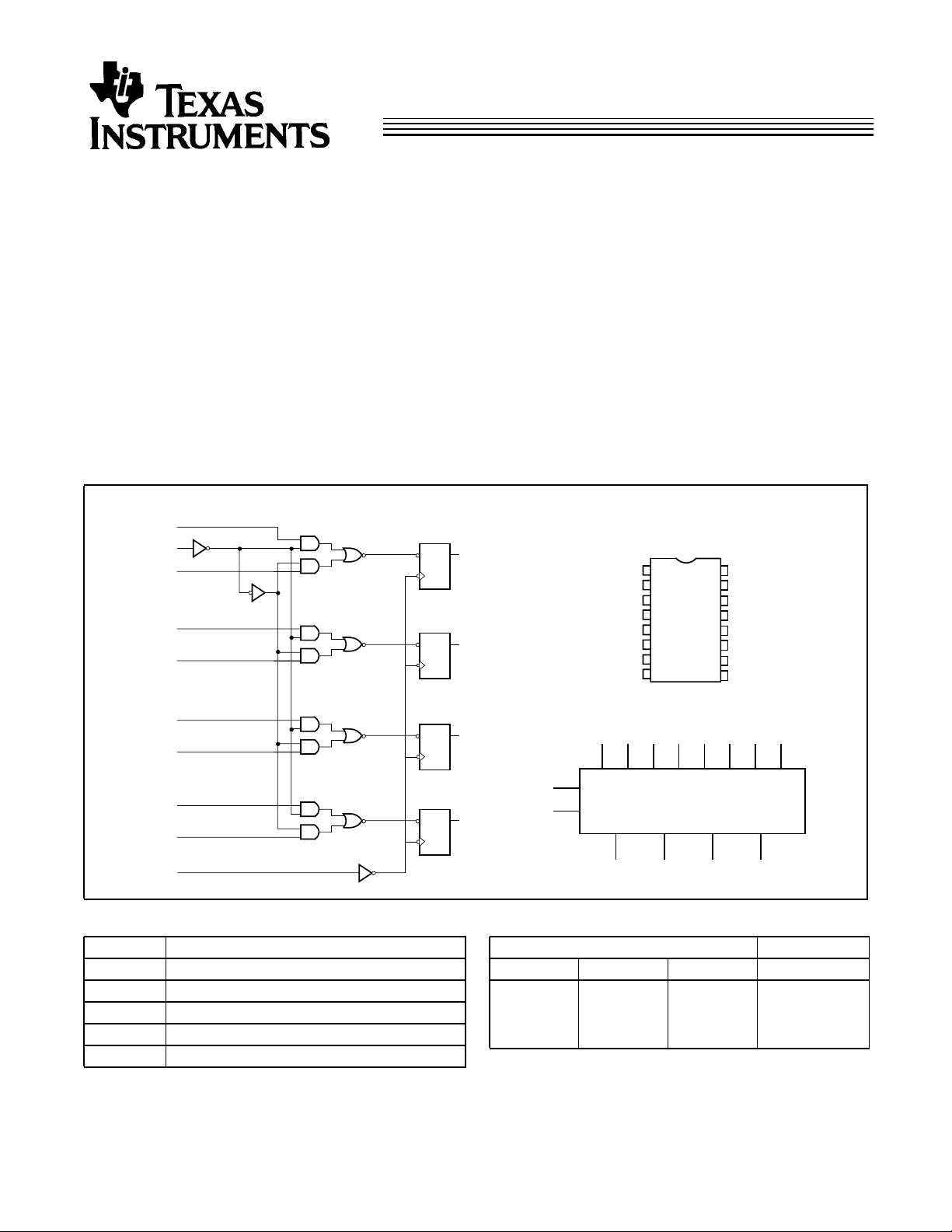
Logic Block Diagram
I
0A
S
I
1A
I
0B
I
1B
D
CP
D
CP
Quad 2-Input Register
Functional Description
The FCT399T is a high-speed quad dual-port register that
selects four bits of data from either of two sources (Ports)
under control of a common Select input (S). The selected data
is transferred to a 4-bit output register synchronous with the
LOW-to-HIGH transition of the Clock input (CP). The 4-bit
D-type output register is fully edge-triggered. The Data inputs
(I
time prior to, and hold time after, the LOW-to-HIGH transition
of the Clock input for predictable operation. The FCT399T
offers true outputs.
The outputs are designed with a power-off disable feature to
allow for liv e insertion of boards.
Q
Q
A
Q
Q
B
) and Select input (S) must be stable only one set-up
0X,I1X
Pin Configurations
SOIC
Top View
S
Q
I
0A
I
1A
I
1B
I
0B
Q
GND
1
A
2
3
4
5
6
B
7
8
V
16
CC
Q
D
15
I
0D
14
I
1D
13
I
1C
12
I
0C
11
Q
10
C
CP
9
I
CP
0C
I
1C
I
0D
I
1D
D
CP
D Q
CP
Q
Pin Description
Name Description
S Common Select Input
CP Clock Pulse Input (Active Rising Edge)
I
0
I
1
Q Register True Outputs
Note:
1. H = HIGH Voltage Level
h = HIGH Voltage Level one set-up time prior to the LOW-to-HIGH Clock Transition
L = LOW Voltage Level
l = LOW Voltage Level one set-up time prior to the LOW-to-HIGH Clock Transition
X = Don’t Care
Data Inputs from Source 0
Data Inputs from Source 1
Q
C
Q
D
Logic Symbol
Function Table
S I
l
l
h
h
I
I
I
I
S
CP
0A
1A
0B
Q
A
1B
Q
B
I0CI1CI0DI
Q
Q
C
1D
D
[1]
Inputs Outputs
0
l
h
X
X
I
1
X
X
l
h
Q
L
H
L
H
Copyright © 2000, Texas Instruments Incorporate

CY74FCT399T
Maximum Ratings
[2, 3]
(Above which the useful life may be impaired. For user guidelines, not tested.)
Storage Temperature .................................–65°C to +150°C
Ambient Temperature with
DC Output Current (Maximum Sink Current/Pin) ......120 mA
Power Dissipation..........................................................0.5W
Static Discharge Voltage............................................>2001V
(per MIL-STD-883, Method 3015)
Operating Range
Power Applied.............................................–65°C to +135°C
Supply Voltage to Ground Potential...............–0.5V to +7.0V
DC Input Voltage............................................–0.5V to +7.0V
Range Range
Commercial All –40°C to +85°C 5V ± 5%
Ambient
Temperature V
DC Output Voltage.........................................–0.5V to +7.0V
Electrical Characteristics Over the Operating Range
Parameter Description Test Conditions Min. Typ.
V
V
V
V
V
V
I
I
I
IH
I
IL
I
OS
I
OFF
OH
OL
IH
IL
H
IK
Output HIGH Voltage VCC=Min., IOH=–32 mA 2.0 V
VCC=Min., IOH=–15 mA 2.4 3.3 V
Output LOW Voltage VCC=Min., IOL=64 mA 0.3 0.55 V
Input HIGH Voltage 2.0 V
Input LOW Voltage 0.8 V
Hysteresis
[5]
All inputs 0.2 V
Input Clamp Diode Voltage VCC=Min., IIN=–18 mA –0.7 –1.2 V
Input HIGH Current VCC=Max., VIN=V
CC
Input HIGH Current VCC=Max., VIN=2.7V ±1 µA
Input LOW Current VCC=Max., VIN=0.5V ±1 µA
Output Short Circuit Current
Power-Off Disable VCC=0V, V
[6]
VCC=Max., V
OUT
=0.0V –60 –120 –225 mA
OUT
=4.5V ±1 µA
[4]
Max. Unit
CC
5 µA
Capacitance
Parameter Description Typ.
C
IN
C
OUT
Notes:
2. Unless otherwise noted, these limits are over the operating free-air temperature range.
3. Unused inputs must always be connected to an appropriate logic voltage level, preferably either V
4. Typical values are at V
5. This parameter is specified but not tested.
6. Not more than one output should be shorted at a time. Duration of short should not exceed one second. The use of high-speed test apparatus and/or sample
and hold techniques is preferable in order to minimize internal chip heating and more accurately reflect operational values. Otherwise prolonged shorting of a
highoutput mayraise thechip temperaturewell above normal and therebycause invalidreadings in other parametrictests. Inany sequence of parameter tests,
tests should be performed last.
I
OS
[5]
[4]
Max. Unit
Input Capacitance 5 10 pF
Output Capacitance 9 12 pF
or ground.
=5.0V, TA=+25˚C ambient.
CC
CC
2
 Loading...