

Texas Instruments CY74FCT2652CTQC, CY74FCT2652ATQCT, CY74FCT2652ATQC Datasheet
8-Bit Registered Transceive
r
CY74FCT2652T
SCCS044 - May 1994 - Revised March 2000
Data sheet acquired from Cypress Semiconductor Corporation.
Data sheet modified to remove devices not offered.
Copyright © 2000, Texas Instruments Incorporated
1CY54/
Features
• Function and pinout compatible with FCT and F logic
• FCT-C speed at 5.4 ns max. (Com’l)
FCT-A speed at 6.3 ns max. (Com’l)
• 25Ωoutputseriesresistorstoreducetransmissionline
reflection noise
• Reduced V
OH
(typically = 3.3V) versions of equivalent
FCT functions
• Edge-rate control circuitry for significantly improved
noise characteristics
• Power-off disable feature
• Matched rise and fall times
• Fully compatible with TTL input and output logic levels
• Sink current 12 mA
Source current 15 mA
• ESD > 2000V
• Independent register for A and B buses
• Multiplexed real-time and stored data transfer
• Extended commercial temp. range of –40˚C to +85˚C
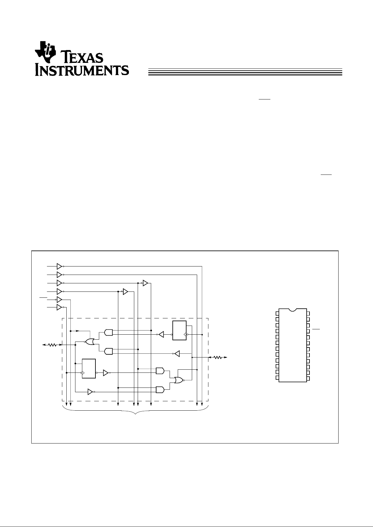
Functional Description
The FCT2652T consists of bus transceiver circuits, D-type
flip-flops, and control circuitry arranged for multiplexed trans-
mission of data directly from the input bus or from the internal
storage registers. GAB and
GBA control pins are provided to
control the transceiver functions. SAB andSBAcontrolpinsare
provided to select either real-time or stored data transf er .
The circuitry used for select control will eliminate the typical
decoding glitch that occurs in a multiplexer during transition
between stored and real-time data. A LOW input level selects
real-time data and a HIGH selects stored data. Data on the A
or B data bus, or both, can be stored in the internal D flip-flops
by LOW-to-HIGH transitions at the appropriate clock pins
(CPAB or CPBA), regardless of the select or enable control
pins. When SAB and SBA are in the real-time transfer mode,
it is also possible to store data without using the internal
D-type flip-flops by simultaneously enabling GAB and
GBA. In
this configuration, each output reinforces its input. Thus, when all
other data sources to the two sets of bus lines are at high impedance, each set of bus lines will remain at its last state .
On-chip termination resistors are added to the outputs to
reduce system noise caused by reflections. The FCT2652T
can replace the FCT652T to reduce noise in existing designs.
The outputs are designed with a power-off disable feature to
allow for live insertion of boards
LogicBlockDiagram Pin Configurations
FCT2652T–1
C
D
B
1
C
D
A
1
TO 7 OTHERCHANNELS
CPAB
SAB
SBA
GBA
GAB
CPBA
BREG
AREG
1OF8
CHANNELS
1
2
3
4
5
6
7
8
9
10
11
12
16
17
18
19
20
24
23
22
21
13
14
V
CC
FCT2652T–3
15
Top View
CPAB
A
1
A
2
A
3
A
4
A
5
A
6
A
7
A
8
B
1
B
2
B
3
B
4
B
5
B
6
B
7
B
8
CPBA
SAB
SBAGAB
GBA
GND
SOIC/QSOP
CY74FCT2652T
2
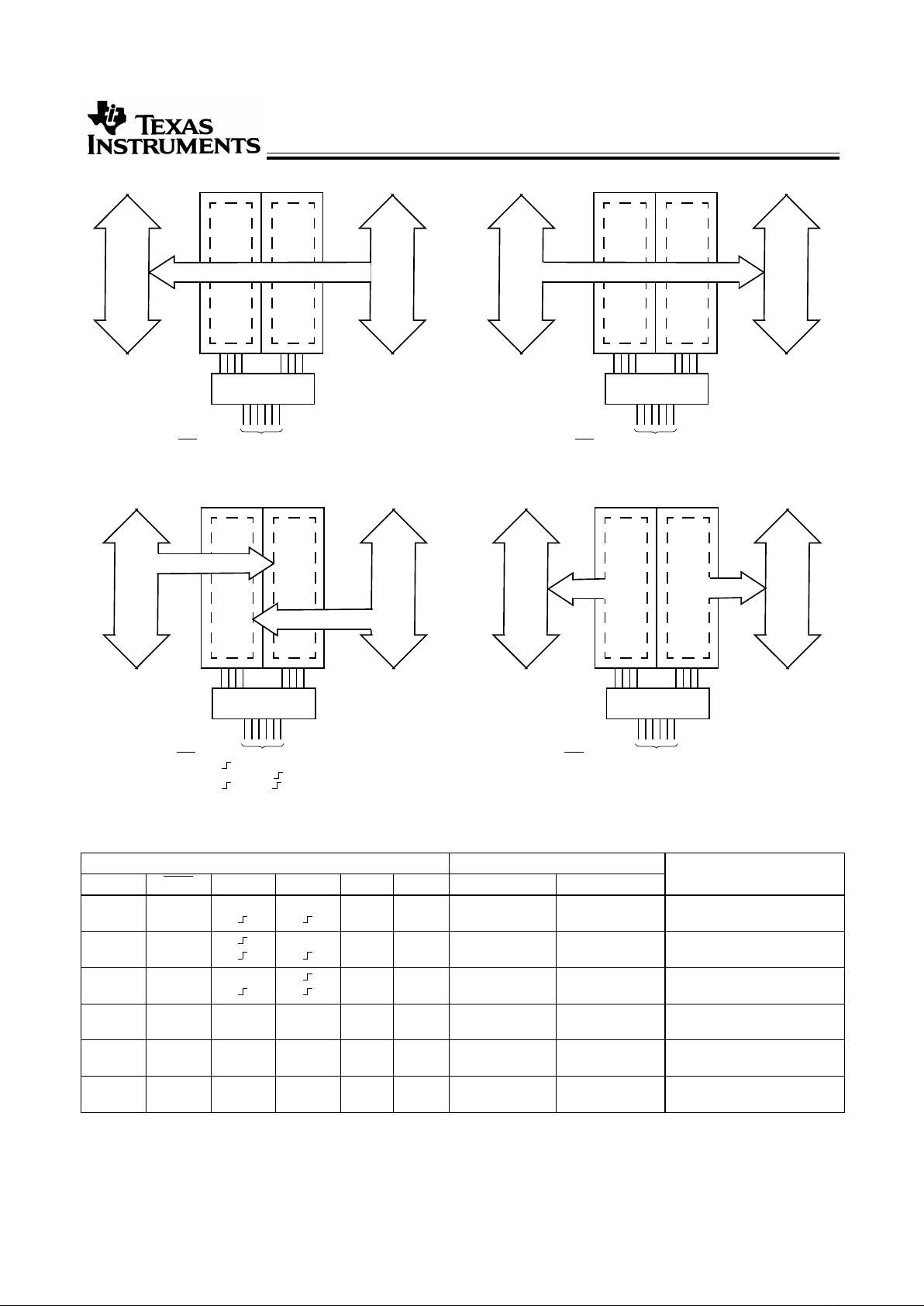
Function Table
[1]
Inputs Data I/O
Operation or FunctionGAB GBA CPAB CPBA SAB SBA A1 thru A
8
B1 thru B
8
L
L
H
H
H or L H or L X
X
X
X
Input Input Isolation
Store A and B Data
X
H
H
H
H or L X
X
[1 ]
X
X
Input
Input
Unspecified
[2]
Output
Store A, Hold B
Store A in both registers
L
L
X
L
H or L X
X
X
X
[1]
Unspecified
[2]
Output
Input
Input
Hold A, Store B
Store B in both registers
L
L
L
L
X
X
X
H or L
X
X
L
H
Output Input Real-Time B Data to A Bus
Stored B Data to A Bus
H
H
H
H
X
H or L
X
X
L
H
X
X
Input Output Real-Time A Data to B Bus
Stored A Data to B Bus
H L H or L H or L H H Output Output Stored A Data to B Bus
and Stored B Data to A Bus
Notes:
1. Select control=L: clocks can occur simultaneously.
Select control=H: clocks must be staggered in order to load both registers. H = HIGH Voltage Level. L = LOW Voltage Level. X = Don’t Care.
BUS BBUS A
GAB
L
GBALCPABXCPBAXSABXSBA
L
BUS
BBUS A
GAB
X
L
L
GBA
H
X
H
CPABXCPBAXSAB
X
X
X
SBA
X
X
X
BUS
BBUS A
GAB
H
GBAHCPABXCPBAXSABLSBA
X
BUS
BBUS A
GAB
H
GBALCPAB
HorL
CPBA
HorL
SABHSBA
H
Real-Time Transfer
Bus B to Bus A
Real-Time
Transfer
Bus A to Bus B
StoreDatafrom A and/or B
Transferred Stored Data
to A and/or B
CY74FCT2652T
3
Maximum Ratings
[3, 4]
(Above which the useful life may be impaired. For user guidelines, not tested.)
Storage Temperature .................................–65°C to +150°C
Ambient Temperature with
Power Applied.............................................–65°C to +135°C
Supply Voltage to Ground Potential............... –0.5V to +7.0V
DC Input Voltage............................................–0.5V to +7.0V
DC Output Voltage......................................... –0.5V to +7.0V
DC Output Current (Maximum Sink Current/Pin.......)120 mA
Power Dissipation..........................................................0.5W
Static Discharge Voltage............................................>2001V
(per MIL-STD-883, Method 3015)
Operating Range
Range
Ambient
Temperature V
CC
Commercial –40°C to +85°C 5V ± 5%
Electrical Characteristics Over the Operating Range
Parameter Description Test Conditions Min. Typ.
[5]
Max. Unit
V
OH
Output HIGH Voltage VCC=Min., IOH=−15 mA 2.4 3.3 V
V
OL
Output LOW Voltage VCC=Min., IOL=12 mA 0.3 0.55 V
R
OUT
Output Resistance VCC=Min., IOL=12 mA 20 25 40 Ω
V
IH
Input HIGH Voltage 2.0 V
V
IL
Input LOW Voltage 0.8 V
V
H
Hysteresis
[6]
All inputs 0.2 V
V
IK
Input Clamp Diode Voltage VCC=Min., IIN=−18 mA –0.7 –1.2 V
I
IH
Input HIGH Current VCC=Max., VIN=V
CC
5 µA
I
IH
Input HIGH Current VCC=Max., VIN=2.7V ±1 µA
I
IL
Input LOW Current VCC=Max., VIN=0.5V ±1 µA
I
OZH
Off State HIGH-Level Output
Current
VCC=Max., V
OUT
=2.7V 10 µA
I
OZL
Off State LOW-Level Output
Current
VCC=Max., V
OUT
=0.5V –10 µA
I
OS
Output Short Circuit Current
[7]
VCC=Max., V
OUT
=0.0V –60 –120 –225 mA
I
OFF
Power-Off Disable VCC=0V, V
OUT
=4.5V ±1 µA
Capacitance
[6]
Parameter Description Test Conditions Typ.
[5]
Max. Unit
C
IN
Input Capacitance 5 10 pF
C
OUT
Output Capacitance 9 12 pF
Notes:
2. The data output functions may be enabledordisabledby various signals at the GAB or GBA inputs. Data input functions are always enabled, i.e.,dataat the
bus pins will be stored on every LOW-to-HIGH transition on the clock inputs.
3. Unless otherwise noted, these limits are over the operating free-air temperature range.
4. Unused inputs must always be connected to an appropriate logic voltage level, preferably either V
CC
or ground.
5. Typical values are at V
CC
=5.0V, TA=+25˚C ambient.
6. This parameter is specified but not tested.
7. Not more than one outputshouldbe shorted at a time. Durationofshort should not exceed onesecond.The use of high-speed test apparatus and/or sample
and hold techniques are preferable in order to minimize internal chip heating and more accurately reflect operational values. Otherwise prolonged shorting
of ahigh output may raisethe chip temperature wellabove normal and therebycause invalid readingsinother parametric tests. Inanysequence of parameter
tests, I
OS
tests should be performed last.
 Loading...