

Texas Instruments CY74FCT245TSOCT, CY74FCT245TSOC, CY74FCT245CTQCT, CY74FCT245CTQC, CY74FCT245ATSOCT Datasheet
...
8-Bit Transceive
r
CY54/74FCT245T
SCCS018 - May 1994 - Revised February 2000
Data sheet acquired from Cypress Semiconductor Corporation.
Data sheet modified to remove devices not offered.
Copyright © 2000, Texas Instruments Incorporated
Features
• Function, pinout, and drive compatible with FCT, and
F logic
• FCT-D speed at 3.8 ns max. (Com’l),
FCT-C speed at 4.1 ns max. (Com’l),
FCT-A speed at 4.6 ns max. (Com’l)
• Reduced V
OH
(typically = 3.3V) versions of equivalent
FCT functions
• Edge-rate control circuitry for significantly improved
noise characteristics
• Power-off disable feature
• ESD > 2000V
• Matched rise and fall times
• Fully compatible with TTL input and output logic levels
• Extended commercial range of −40˚C to +85˚C
• Sink current 64 mA (Com’l), 48 mA (Mil)
Source current 32 mA (Com’l), 12 mA (Mil)
Functional Description
The FCT245T contains eight non-inverting bidirectional buffers with three-state outputs and is intended for bus oriented
applications. For the FCT245T,current sinking capability is 64
mA at the A and B ports.
The Transmit/Receiver (T/
R) input determines the direction of
data flow through bidirectional transceiver. Transmit (Active
HIGH)enablesdatafromAports to Bports. The output enable
(
OE), when HIGH, disables both the A and B ports by putting
them in a High Z condition.
The outputs are designed with a power-off disable feature to
allow for live insertion of boards.
Function Table
[1]
OE T/R Operation
L L B Data to Bus A
L H A Data to Bus B
H X High Z State
Note:
1. H = HIGH Voltage Level. L = LOW Voltage Level. X = Don’t Care.
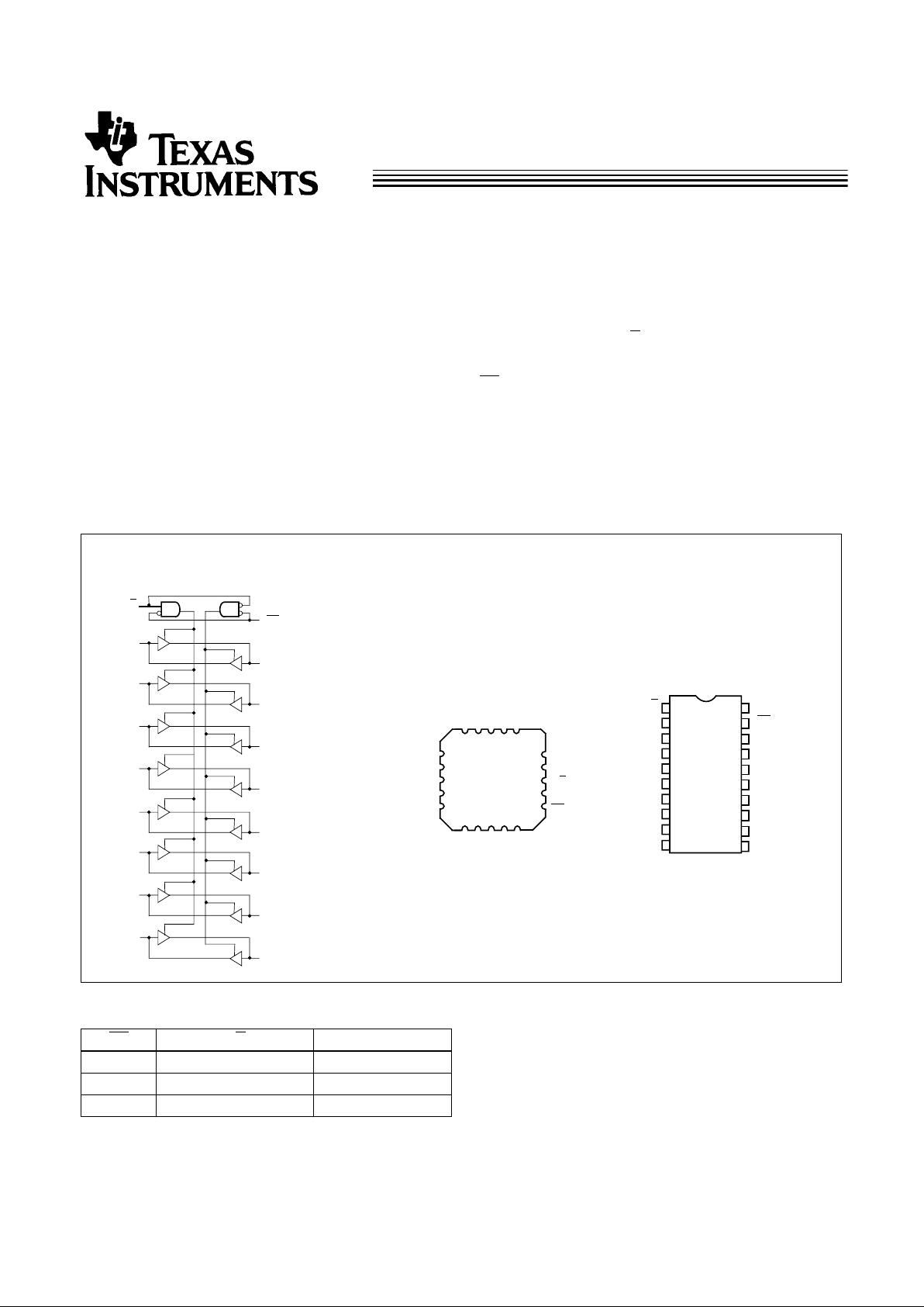
LogicBlockDiagram Pin Configurations
A
0
A
1
A
2
A
3
A
4
A
5
A
6
A
7
OE
B
0
B
1
B
2
B
3
B
4
B
5
B
6
B
7
T/R
4
8
9
10
11
12
765
1516 17 18
3
2
1
20
13
14
19
A6A5A
3
B
1
B
4
B
0
B
7
V
CC
GND
B
3
Top View
A
2
LCC
T/R
A
0
A
1
A
7
B
5
B
6
1
2
3
4
5
6
7
8
9
10
11
12
16
17
18
19
20
13
14
V
CC
15
Top View
B
2
A
4
OE
A
0
A
1
A
2
A
3
A
4
A
5
A
6
A
7
OE
B
0
B
1
B
2
B
3
B
4
B
5
B
6
B
7
T/R
GND
DIP/SOIC/QSOP
CY54/74FCT245T
2
Maximum Ratings
[2,3]
(Above which the useful life may be impaired. For user
guidelines, not tested.)
Storage Temperature .....................................−65°C to +150°C
Ambient Temperature with
Power Applied..................................................−65°C to +135°C
Supply Voltage to Ground Potential..................−0.5V to +7.0V
DC Input Voltage .................................................−0.5V to +7.0V
DC Output Voltage..............................................−0.5V to +7.0V
DC Output Current (Maximum Sink Current/Pin).......120 mA
Power Dissipation..........................................................0.5W
Static Discharge Voltage............................................>2001V
(per MIL-STD-883, Method 3015)
Operating Range
Range Range
Ambient
Temperature V
CC
Commercial DT 0°C to +70°C 5V ± 5%
Commercial T, AT, CT −40°C to +85°C 5V ± 5%
Military
[4]
All −55°C to +125°C 5V ± 10%
Electrical Characteristics Over the Operating Range
Parameter Description Test Conditions Min. Typ.
[5]
Max. Unit
V
OH
Output HIGH Voltage VCC=Min., IOH=−32 mA Com’l 2.0 V
VCC=Min., IOH=−15 mA Com’l 2.4 3.3 V
VCC=Min., IOH=−12 mA Mil 2.4 3.3 V
V
OL
Output LOW Voltage VCC=Min., IOL=64 mA Com’l 0.3 0.55 V
VCC=Min., IOL=48mA Mil 0.3 0.55 V
V
IH
Input HIGH Voltage 2.0 V
V
IL
Input LOW Voltage 0.8 V
V
H
Hysteresis
[6]
All inputs 0.2 V
V
IK
Input Clamp Diode Voltage VCC=Min., IIN=−18 mA −0.7 −1.2 V
I
I
Input HIGH Current VCC=Max., VIN=V
CC
5 µA
I
IH
Input HIGH Current VCC=Max., VIN=2.7V ±1 µA
I
IL
Input LOW Current VCC=Max., VIN=0.5V ±1 µA
I
OS
Output Short Circuit Current
[7]
VCC=Max., V
OUT
=0.0V −60 −120 −225 mA
I
OFF
Power-Off Disable VCC=0V, V
OUT
=4.5V ±1 µA
Capacitance
[6]
Parameter Description Typ.
[5]
Max. Unit
C
IN
Input Capacitance 5 10 pF
C
OUT
Output Capacitance 9 12 pF
Notes:
2. Unless otherwise noted, these limits are over the operating free-air temperature range.
3. Unused inputs must always be connected to an appropriate logic voltage level, preferably either V
CC
or ground.
4. T
A
is the “instant on” case temperature.
5. Typical values are at V
CC
=5.0V, TA=+25˚C ambient.
6. This parameter is specified but not tested.
7. Not morethan one output shouldbe shorted at a time.Duration of short should notexceed one second.The use of high-speedtest apparatus and/or sample
and holdtechniques are preferablein order tominimize internal chip heatingand more accurately reflect operational values.Otherwise prolonged shorting of
a high output mayraise the chip temperature well abovenormal and thereby cause invalid readings in other parametric tests. In any sequence of parameter
tests, I
OS
tests should be performed last.
CY54/74FCT245T
3
Power Supply Characteristics
Parameter Description Test Conditions Typ.
[5]
Max. Unit
I
CC
Quiescent Power Supply Current VCC=Max., VIN≤0.2V, VIN≥VCC−0.2V 0.1 0.2 mA
∆I
CC
Quiescent Power Supply Current
(TTL inputs HIGH)
VCC=Max., VIN=3.4V,
[8]
f1=0, Outputs Open
0.5 2.0 mA
I
CCD
Dynamic Power Supply Current
[9]
VCC=Max., One Input Toggling,
50% Duty Cycle, Outputs Open,
T/
R or OE=GND and
V
IN
≤0.2V or VIN≥VCC−0.2V
0.06 0.12 mA/MHz
I
C
Total Power Supply Current
[10]
VCC=Max.,50% DutyCycle,OutputsOpen,
One Bit Toggling at f
1
=10 MHz,
T/
R or OE=GND and
V
IN
≤0.2V or VIN≥VCC−0.2V
0.7 1.4 mA
VCC=Max.,50% DutyCycle,OutputsOpen,
One Bit Toggling at f
1
=10 MHz,
T/
RorOE=GND and VIN=3.4VorVIN=GND
1.2 3.4 mA
VCC=Max.,50% DutyCycle,OutputsOpen,
Eight Bits Toggling at f
1
=2.5 MHz,
T/
R or OE=GND and
V
IN
≤0.2V or VIN≥VCC−0.2V
1.3 2.6
[11]
mA
VCC=Max.,50% DutyCycle,OutputsOpen,
Eight Bits Toggling at f
1
=2.5 MHz,
T/
RorOE=GND and VIN=3.4VorVIN=GND
3.3 10.6
[11]
mA
Notes:
8. Per TTL driven input (V
IN
=3.4V); all other inputs at VCC or GND.
9. This parameter is not directly testable, but is derived for use in Total Power Supply calculations.
10. I
C
=I
QUIESCENT
+ I
INPUTS
+ I
DYNAMIC
IC=ICC+∆ICCDHNT+I
CCD(f0
/2 + f1N1)
I
CC
= Quiescent Current with CMOS input levels
∆I
CC
= Power Supply Current for a TTL HIGH input (VIN=3.4V)
D
H
= Duty Cycle for TTL inputs HIGH
N
T
= Number of TTL inputs at D
H
I
CCD
= Dynamic Current caused by an input transition pair (HLH or LHL)
f
0
= Clock frequency for registered devices, otherwise zero
f
1
= Input signal frequency
N
1
= Number of inputs changing at f
1
All currents are in milliamps and all frequencies are in megahertz.
11. Values for these conditions are examples of the ICC formula. These limits are specified but not tested.

CY54/74FCT245T
4
Document #: 38−00318−B
Switching Characteristics Over the Operating Range
Parameter Description
FCT245T FCT245AT
Unit
Fig.
No.
[13]
Military Commercial Military Commercial
Min.
[12]
Max. Min.
[12]
Max. Min.
[12]
Max. Min.
[12]
Max.
t
PLH
t
PHL
Propagation Delay
A to B or B to A
1.5 7.5 1.5 7.0 1.5 4.9 1.5 4.6 ns 1, 3
t
PZH
t
PZL
Output Enable Time
OE or T/R to A or B
1.5 10.0 1.5 9.5 1.5 6.5 1.5 6.2 ns 1, 7, 8
t
PHZ
t
PLZ
Output Disable Time
OE or T/R to A or B
1.5 10.0 1.5 7.5 1.5 6.0 1.5 5.0 ns 1, 7, 8
Switching Characteristics Over the Operating Range (continued)
Parameter Description
FCT245CT FCT245DT
Unit
Fig.
No.
[13]
Military Commercial Commercial
Min.
[12]
Max. Min.
[12]
Max. Min.
[12]
Max.
t
PLH
t
PHL
Propagation Delay
A to B or B to A
1.5 4.5 1.5 4.1 1.5 3.8 ns 1, 3
t
PZH
t
PZL
Output Enable Time
OE or T/R to A or B
1.5 6.2 1.5 5.8 1.5 5.0 ns 1, 7, 8
t
PHZ
t
PLZ
Output Disable Time
OE or T/R to A or B
1.5 5.2 1.5 4.8 1.5 4.3 ns 1, 7, 8
Ordering Information
Speed
(ns) Ordering Code
Package
Name Package Type
Operating
Range
3.8 CY74FCT245DTQCT Q5 20-Lead (150-Mil) QSOP Commercial
CY74FCT245DTSOC/SOCT S5 20-Lead (300-Mil) Molded SOIC
4.1 CY74FCT245CTQCT Q5 20-Lead (150-Mil) QSOP Commercial
CY74FCT245CTSOC/SOCT S5 20-Lead (300-Mil) Molded SOIC
4.5 CY54FCT245CTDMB D6 20-Lead (300-Mil) CerDIP Military
CY54FCT245CTLMB L61 20-Square Leadless Chip Carrier
4.6 CY74FCT245ATPC P5 20-Lead (300-Mil) Molded DIP Commercial
CY74FCT245ATQCT Q5 20-Lead (150-Mil) QSOP
CY74FCT245ATSOC/SOCT S5 20-Lead (300-Mil) Molded SOIC
4.9 CY54FCT245ATDMB D6 20-Lead (300-Mil) CerDIP Military
CY54FCT245ATLMB L61 20-Square Leadless Chip Carrier
7.0 CY74FCT245TQCT Q5 20-Lead (150-Mil) QSOP Commercial
CY74FCT245TSOC/SOCT S5 20-Lead (300-Mil) Molded SOIC
7.5 CY54FCT245TDMB D6 20-Lead (300-Mil) CerDIP Military
CY54FCT245TLMB L61 20-Square Leadless Chip Carrier
Notes:
12. Minimum limits are specified but not tested on Propagation Delays.
13. See “Parameter Measurement Information” in the General Information section.
CY54/74FCT245T
5
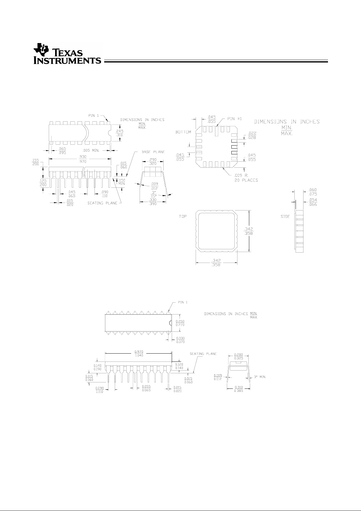
Package Diagrams
20-Lead (300-Mil) CerDIP D6
MIL−STD−1835 D−8 Config.A
20-Pin Square Leadless Chip Carrier L61
MIL−STD−1835 C−2A
20-Lead (300-Mil) Molded DIP P5
CY54/74FCT245T
6
Package Diagrams (continued)
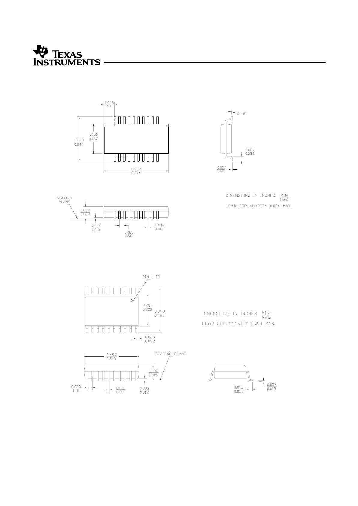
20-Lead Quarter Size Outline
Q5
20-Lead (300-Mil) Molded SOIC
S5

IMPORTANT NOTICE
T exas Instruments and its subsidiaries (TI) reserve the right to make changes to their products or to discontinue
any product or service without notice, and advise customers to obtain the latest version of relevant information
to verify, before placing orders, that information being relied on is current and complete. All products are sold
subject to the terms and conditions of sale supplied at the time of order acknowledgement, including those
pertaining to warranty, patent infringement, and limitation of liability.
TI warrants performance of its semiconductor products to the specifications applicable at the time of sale in
accordance with TI’s standard warranty. Testing and other quality control techniques are utilized to the extent
TI deems necessary to support this warranty. Specific testing of all parameters of each device is not necessarily
performed, except those mandated by government requirements.
CERT AIN APPLICATIONS USING SEMICONDUCTOR PRODUCTS MA Y INVOLVE POTENTIAL RISKS OF
DEATH, PERSONAL INJURY, OR SEVERE PROPERTY OR ENVIRONMENTAL DAMAGE (“CRITICAL
APPLICATIONS”). TI SEMICONDUCTOR PRODUCTS ARE NOT DESIGNED, AUTHORIZED, OR
WARRANTED TO BE SUITABLE FOR USE IN LIFE-SUPPORT DEVICES OR SYSTEMS OR OTHER
CRITICAL APPLICATIONS. INCLUSION OF TI PRODUCTS IN SUCH APPLICA TIONS IS UNDERSTOOD T O
BE FULLY AT THE CUSTOMER’S RISK.
In order to minimize risks associated with the customer’s applications, adequate design and operating
safeguards must be provided by the customer to minimize inherent or procedural hazards.
TI assumes no liability for applications assistance or customer product design. TI does not warrant or represent
that any license, either express or implied, is granted under any patent right, copyright, mask work right, or other
intellectual property right of TI covering or relating to any combination, machine, or process in which such
semiconductor products or services might be or are used. TI’s publication of information regarding any third
party’s products or services does not constitute TI’s approval, warranty or endorsement thereof.
Copyright 2000, Texas Instruments Incorporated
 Loading...