

Page 1

CD4066BC,CD4066BM
CD4066BM CD4066BC Quad Bilateral Switch
Literature Number: SNOS366A
Page 2
CD4066BM/CD4066BC Quad Bilateral Switch
Obsolete
CD4066BM/CD4066BC Quad Bilateral Switch
June 1992
General Description
The CD4066BM/CD4066BC is a quad bilateral switch intended for the transmission or multiplexing of analog or digital signals. It is pin-for-pin compatible with CD4016BM/
CD4016BC, but has a much lower ‘‘ON’’ resistance, and
‘‘ON’’ resistance is relatively constant over the input-signal
range.
Features
Y
Wide supply voltage range 3V to 15V
Y
High noise immunity 0.45 VDD(typ.)
Y
Wide range of digital and
analog switching
Y
‘‘ON’’ resistance for 15V operation 80X
Y
Matched ‘‘ON’’ resistance DR
over 15V signal input
Y
‘‘ON’’ resistance flat over peak-to-peak signal range
Y
High ‘‘ON’’/‘‘OFF’’ 65 dB (typ.)
output voltage ratio
Y
High degree linearity 0.1% distortion (typ.)
High degree linearity
High degree linearity V
DD
@
e
f
is
@
f
is
b
V
10 kHz, R
e
1 kHz, V
e
10V, R
SS
ON
g
7.5 V
e
L
is
L
PEAK
5X (typ.)
e
10 kX
e
5V
p-p
e
10 kX
,
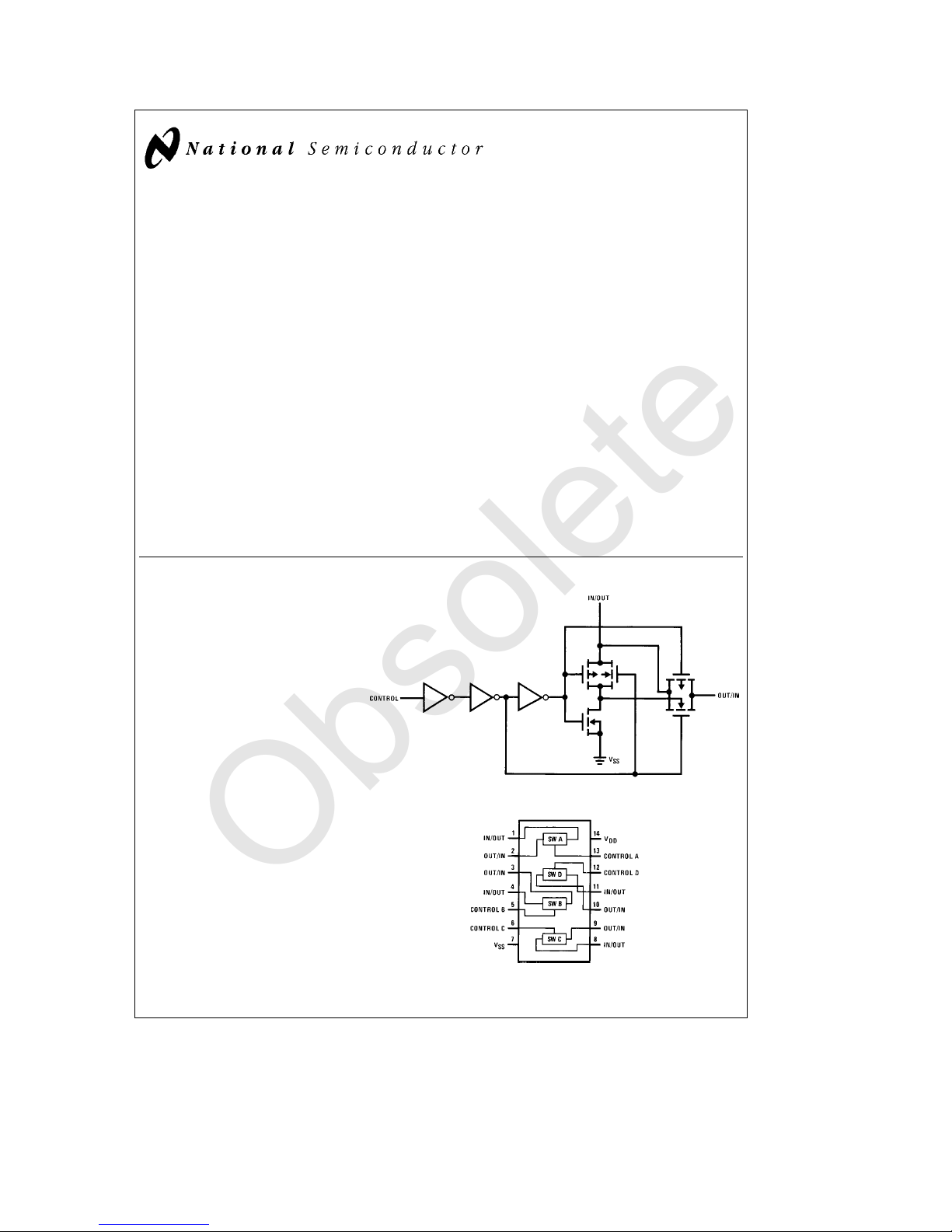
Schematic and Connection Diagrams
Y
Extremely low ‘‘OFF’’ 0.1 nA (typ.)
switch leakage
Y
Extremely high control input impedance 1012X(typ.)
Y
Low crosstalk
between switches
Y
Frequency response, switch ‘‘ON’’ 40 MHz (typ.)
@
b
DD
@
V
SS
e
f
0.9 MHz, R
is
e
10V, T
b
A
50 dB (typ.)
L
V
Applications
Y
Analog signal switching/multiplexing
Signal gating
#
Squelch control
#
Chopper
#
Modulator/Demodulator
#
Commutating switch
#
Y
Digital signal switching/multiplexing
Y
CMOS logic implementation
Y
Analog-to-digital/digital-to-analog conversion
Y
Digital control of frequency, impedance, phase, and analog-signal-gain
e
e
25§C
1kX
Order Number CD4066B
C
1995 National Semiconductor Corporation RRD-B30M105/Printed in U. S. A.
TL/F/5665
Dual-In-Line Package
TL/F/5665– 1
Top View
Page 3
Absolute Maximum Ratings (Notes1&2)
Obsolete
If Military/Aerospace specified devices are required,
please contact the National Semiconductor Sales
Office/Distributors for availability and specifications.
Supply Voltage (V
Input Voltage (VIN)
Storage Temperature Range (T
Power Dissipation (PD)
Dual-In-Line 700 mW
Small Outline 500 mW
Lead Temperature (T
(Soldering, 10 seconds) 300
DD
)
)
S
)
L
b
0.5V toa18V
b
0.5V to V
b
65§Ctoa150§C
DD
a
0.5V
C
§
DC Electrical Characteristics CD4066BM (Note 2)
Symbol Parameter Conditions
I
DD
SIGNAL INPUTS AND OUTPUTS
R
DR
I
IS
CONTROL INPUTS
V
V
I
IN
Quiescent Device Current V
‘‘ON’’ Resistance R
ON
D‘‘ON’’ Resistance R
ON
Between any 2 of V
4 Switches V
Input or Output Leakage V
Switch ‘‘OFF’’ V
Low Level Input Voltage V
ILC
High Level Input Voltage V
IHC
Input Current V
e
5V 0.25 0.01 0.25 7.5 mA
DD
e
V
10V 0.5 0.01 0.5 15 mA
DD
e
V
15V 1.0 0.01 1.0 30 mA
DD
b
V
V
DD
e
V
e
15V
SS
SS
2
VSSto V
b
V
DD
2
VSSto V
DD
SS
SS
SS
e
10 kX to
L
e
V
VDD,V
C
V
DD
V
DD
V
DD
L
C
DD
V
DD
C
IS
V
OS
IS
V
OS
I
IS
V
DD
V
DD
V
DD
DD
V
DD
V
DD
DD
V
DD
V
DD
IS
e
5V 800 270 1050 1300 X
e
10V 310 120 400 550 X
e
15V 200 80 240 320 X
e
10 kX to
e
VDD,V
IS
e
10V 10 X
e
15V 5 X
e
0
e
15V and 0V,
e
0V and 15V
e
VSSand V
e
VDDand V
e
g
10 mA
e
5V 1.5 2.25 1.5 1.5 V
e
10V 3.0 4.5 3.0 3.0 V
e
15V 4.0 6.75 4.0 4.0 V
e
5V 3.5 3.5 2.75 3.5 V
e
10V (see note 6) 7.0 7.0 5.5 7.0 V
e
15V 11.0 11.0 8.25 11.0 V
b
e
V
SS
t
t
V
V
IS
t
t
V
V
C
Recommended Operating
Conditions
Supply Voltage (VDD) 3Vto15V
Input Voltage (VIN) 0VtoV
Operating Temperature Range (TA)
CD4066BM
CD4066BC
b
55§C
Min Max Min Typ Max Min Max
DD
DD
g
50
g
0.1
(Note 2)
a
g
g
10
25§C
0.1g50
b
5
g
0.1
b
55§Ctoa125§C
b
40§Ctoa85§C
a
125§C
g
500 nA
g
1.0 mA
DD
Units
DC Electrical Characteristics CD4066BC (Note 2)
Symbol Parameter Conditions
I
DD
Quiescent Device Current V
V
V
b
40§C
Min Max Min Typ Max Min Max
e
5V 1.0 0.01 1.0 7.5 mA
DD
e
10V 2.0 0.01 2.0 15 mA
DD
e
15V 4.0 0.01 4.0 30 mA
DD
2
a
25§C
a
85§C
Units
Page 4

DC Electrical Characteristics (Continued) CD4066BC (Note 2)
Obsolete
b
Symbol Parameter Conditions
SIGNAL INPUTS AND OUTPUTS
R
DR
I
‘‘ON’’ Resistance R
ON
D‘‘ON’’ Resistance R
ON
Between Any 2 of V
4 Switches V
IS
Input or Output Leakage V
Switch ‘‘OFF’’
e
L
e
V
C
e
V
DD
e
V
DD
e
V
DD
e
L
e
CC
e
DD
e
V
DD
e
C
V
10 kX to
VDD,VSSto V
5V 850 270 1050 1200 X
10V 330 120 400 520 X
15V 210 80 240 300 X
V
10 kX to
e
VDD,V
IS
10V 10 X
15V 5 X
0
CONTROL INPUTS
V
V
I
IN
Low Level Input Voltage V
ILC
High Level Input Voltage V
IHC
Input Current V
e
VSSand V
IS
e
V
VDDand V
OS
e
g
I
10mA
IS
e
V
5V 1.5 2.25 1.5 1.5 V
DD
e
V
10V 3.0 4.5 3.0 3.0 V
DD
e
V
15V 4.0 6.75 4.0 4.0 V
DD
e
5V 3.5 3.5 2.75 3.5 V
DD
e
V
10V (See note 6) 7.0 7.0 5.5 7.0 V
DD
e
V
15V 11.0 11.0 8.25 11.0 V
DD
b
e
V
DD
V
DD
V
DD
15V
SS
t
t
V
V
IS
SS
t
t
V
V
C
SS
b
DD
2
DD
b
DD
2
VSSto V
DD
SS
V
SS
V
SS
DD
40§C
Min Max Min Typ Max Min Max
a
25§C
g
50
g
0.3
g
0.1g50
b
g
10
5
g
0.3
a
85§C
g
200 nA
g
Units
1.0 mA
AC Electrical Characteristics* T
e
A
e
e
C, t
t
r
20 ns and V
f
25
§
e
0V unless otherwise noted
SS
Symbol Parameter Conditions Min Typ Max Units
t
PHL,tPLH
t
PZH,tPZL
t
PHZ,tPLZ
Propagation Delay Time Signal V
Input to Signal Output R
Propagation Delay Time R
Control Input to Signal V
Output High Impedance to V
Logical Level V
Propagation Delay Time R
Control Input to Signal V
Output Logical Level to V
High Impedance V
Sine Wave Distortion V
Frequency Response-Switch V
‘‘ON’’ (Frequency at
b
3 dB) R
e
C
e
L
V
DD
V
DD
V
DD
e
L
DD
DD
DD
e
L
DD
DD
DD
e
C
e
R
L
(
Figure 4
e
C
e
L
20 Log
(
Figure 4
e
VDD,C
200k
e
e
e
1.0 kX,C
e
e
e
1.0 kX,C
e
e
e
V
10 kX,V
V
1kX,V
50 pF, (
Figure 1
L
)
5V 25 55 ns
10V 15 35 ns
15V 10 25 ns
e
50 pF, (
L
5V 125 ns
Figures 2
and3)
10V 60 ns
15V 50 ns
e
50 pF, (
L
5V 125 ns
Figures 2
and3)
10V 60 ns
15V 50 ns
e
DD
)
e
DD
10VOS/VOS
)
5V, V
IS
5V, V
IS
SS
e
5V
SS
e
5V
eb
5V 0.1 %
,fe1 kHz,
p-p
eb
5V, 40 MHz
,
p-p
(1 kHz)bdB,
3
Page 5

AC Electrical Characteristics* (Continued) T
Obsolete
Symbol Parameter Conditions Min Typ Max Units
Feedthrough Ð Switch ‘‘OFF’’ V
(Frequency at
Crosstalk Between Any Two V
Switches (Frequency at
Crosstalk; Control Input to V
Signal Output V
Maximum Control Input R
C
IS
C
OS
C
IOS
C
IN
*AC Parameters are guaranteed by DC correlated testing.
Note 1: ‘‘Absolute Maximum Ratings’’ are those values beyond which the safety of the device cannot be guaranteed. They are not meant to imply that the devices
should be operated at these limits. The tables of ‘‘Recommended Operating Conditions’’ and ‘‘Electrical Characteristics’’ provide conditions for actual device
operation.
Note 2: V
Note 3: These devices should not be connected to circuits with the power ‘‘ON’’.
Note 4: In all cases, there is approximately 5 pF of probe and jig capacitance in the output; however, this capacitance is included in C
Note 5: V
Note 6: Conditions for V
Signal Input Capacitance 8.0 pF
Signal Output Capacitance V
Feedthrough Capacitance V
Control Input Capacitance 5.0 7.5 pF
e
0V unless otherwise specified.
SS
is the voltage at the in/out pin and VOSis the voltage at the out/in pin. VCis the voltage at the control input.
IS
b
50 dB) R
e
:a)V
IHC
VDD,I
IS
b
50 dB) RL1kX,V
e
standard B series IOHb) V
OS
e
DD
e
1kX,V
L
V
OS/VIS
e
DD
V
OS(B)/VIS(A)
e
DD
e
CC
(Figure 6)
e
1.0 kX,C
L
V
OS(f)
e
V
DD
e
V
DD
e
V
DD
e
DD
e
0V 0.5 pF
C
e
A
5.0V, V
CC
e
IS
eb
50 dB,
e
V
5.0V; V
C(A)
e
IS(A)
eb
e
10V, R
L
10V Square Wave, C
e
L
e
(/2 VOS(1.0 kHz)
5.0V 6.0 MHz
10V 8.0 MHz
15V 8.5 MHz
10V 8.0 pF
e
0V, I
IS
e
25§C, t
r
e
eb
V
SS
5.0V
,20Log10,
p-p
(Figure 4)
e
SS
5.0 V
,20Log10,
p-p
50 dB
(Figure 5)
10 kX,R
50 pF,
(Figure 7)
e
standard B series IOL.
OL
e
t
20 ns and V
f
5.0V, 1.25
e
V
5.0V, 0.9 MHz
C(B)
e
1.0 kX, 150 mV
IN
e
50 pF
L
e
0V unless otherwise noted
SS
wherever it is specified.
L
AC Test Circuits and Switching Time Waveforms
p-p
FIGURE 1. t
FIGURE 2. t
FIGURE 3. t
PHL,tPLH
PZH,tPHZ
PZL,tPLZ
Propagation Delay Time Signal Input to Signal Output
Propagation Delay Time Control to Signal Output
TL/F/5665– 2
Propagtion Delay Time Control to Signal Output
4
Page 6

AC Test Circuits and Switching Time Waveforms (Continued)
Obsolete
e
V
VDDfor distortion and frequency response tests
C
e
V
VSSfor feedthrough test
C
FIGURE 4. Sine Wave Distortion, Frequency Response and Feedthrough
FIGURE 5. Crosstalk Between Any Two Switches
FIGURE 6. Crosstalk: Control Input to Signal Output
FIGURE 7. Maximum Control Input Frequency
5
TL/F/5665– 3
Page 7

Typical Performance Characteristics
Obsolete
‘‘ON’’ Resistance vs Signal
Voltage for T
e
25§C
A
‘‘ON’’ Resistance as a Function
of Temperature for
b
DD
e
V
15V
SS
V
‘‘ON’’ Resistance as a Function
of Temperature for
b
DD
e
V
10V
SS
V
Special Considerations
In applications where separate power sources are used to
drive V
should exceed V
CD4066BM/CD4066BC bilateral switches). This provision
avoids any permanent current flow or clamp action of the
V
CD4066BM/CD4066BC.
In certain applications, the external load-resistor current
may include both V
and the signal input, the VDDcurrent capability
DD
DD/RL(RL
supply when power is applied or removed from
DD
e
effective external load of the 4
and signal-line components. To avoid
DD
‘‘ON’’ Resistance as a Function
of Temperature for
b
V
drawing V
nals 1, 4, 8 or 11, the voltage drop across the bidirectional
switch must not exceed 0.6V at T
T
No VDDcurrent will flow through RLif the switch current
flows into terminals 2, 3, 9 or 10.
DD
l
25§C (calculated from RONvalues shown).
A
e
V
DD
current when switch current flows into termi-
5V
SS
TL/F/5665– 4
s
25§C, or 0.4V at
A
6
Page 8

Physical Dimensions inches (millimeters)
Obsolete
Order Number CD4066BMJ or CD4066BCJ
Cerdip (J)
NS Package Number J14A
S.O. Package (M)
Order Number CD4066BCM
NS Package Number M14A
7
Page 9

Physical Dimensions inches (millimeters) (Continued)
Obsolete
Order Number CD4066BMN or CD4066BCN
Dual-In-Line Package (N)
NS Package Number N14A
CD4066BM/CD4066BC Quad Bilateral Switch
LIFE SUPPORT POLICY
NATIONAL’S PRODUCTS ARE NOT AUTHORIZED FOR USE AS CRITICAL COMPONENTS IN LIFE SUPPORT
DEVICES OR SYSTEMS WITHOUT THE EXPRESS WRITTEN APPROVAL OF THE PRESIDENT OF NATIONAL
SEMICONDUCTOR CORPORATION. As used herein:
1. Life support devices or systems are devices or 2. A critical component is any component of a life
systems which, (a) are intended for surgical implant support device or system whose failure to perform can
into the body, or (b) support or sustain life, and whose be reasonably expected to cause the failure of the life
failure to perform, when properly used in accordance support device or system, or to affect its safety or
with instructions for use provided in the labeling, can effectiveness.
be reasonably expected to result in a significant injury
to the user.
National Semiconductor National Semiconductor National Semiconductor National Semiconductor
Corporation Europe Hong Kong Ltd. Japan Ltd.
1111 West Bardin Road Fax: (
Arlington, TX 76017 Email: cnjwge@tevm2.nsc.com Ocean Centre, 5 Canton Rd. Fax: 81-043-299-2408
Tel: 1(800) 272-9959 Deutsch Tel: (
Fax: 1(800) 737-7018 English Tel: (
National does not assume any responsibility for use of any circuitry described, no circuit patent licenses are implied and National reserves the right at any time without notice to change said circuitry and specifications.
Fran3ais Tel: (
Italiano Tel: (
a
49) 0-180-530 85 86 13th Floor, Straight Block, Tel: 81-043-299-2309
a
49) 0-180-530 85 85 Tsimshatsui, Kowloon
a
49) 0-180-532 78 32 Hong Kong
a
49) 0-180-532 93 58 Tel: (852) 2737-1600
a
49) 0-180-534 16 80 Fax: (852) 2736-9960
Page 10

IMPORTANT NOTICE
Texas Instruments Incorporated and its subsidiaries (TI) reserve the right to make corrections, modifications, enhancements, improvements,
and other changes to its products and services at any time and to discontinue any product or service without notice. Customers should
obtain the latest relevant information before placing orders and should verify that such information is current and complete. All products are
sold subject to TI’s terms and conditions of sale supplied at the time of order acknowledgment.
TI warrants performance of its hardware products to the specifications applicable at the time of sale in accordance with TI’s standard
warranty. Testing and other quality control techniques are used to the extent TI deems necessary to support this warranty. Except where
mandated by government requirements, testing of all parameters of each product is not necessarily performed.
TI assumes no liability for applications assistance or customer product design. Customers are responsible for their products and
applications using TI components. To minimize the risks associated with customer products and applications, customers should provide
adequate design and operating safeguards.
TI does not warrant or represent that any license, either express or implied, is granted under any TI patent right, copyright, mask work right,
or other TI intellectual property right relating to any combination, machine, or process in which TI products or services are used. Information
published by TI regarding third-party products or services does not constitute a license from TI to use such products or services or a
warranty or endorsement thereof. Use of such information may require a license from a third party under the patents or other intellectual
property of the third party, or a license from TI under the patents or other intellectual property of TI.
Reproduction of TI information in TI data books or data sheets is permissible only if reproduction is without alteration and is accompanied
by all associated warranties, conditions, limitations, and notices. Reproduction of this information with alteration is an unfair and deceptive
business practice. TI is not responsible or liable for such altered documentation. Information of third parties may be subject to additional
restrictions.
Resale of TI products or services with statements different from or beyond the parameters stated by TI for that product or service voids all
express and any implied warranties for the associated TI product or service and is an unfair and deceptive business practice. TI is not
responsible or liable for any such statements.
TI products are not authorized for use in safety-critical applications (such as life support) where a failure of the TI product would reasonably
be expected to cause severe personal injury or death, unless officers of the parties have executed an agreement specifically governing
such use. Buyers represent that they have all necessary expertise in the safety and regulatory ramifications of their applications, and
acknowledge and agree that they are solely responsible for all legal, regulatory and safety-related requirements concerning their products
and any use of TI products in such safety-critical applications, notwithstanding any applications-related information or support that may be
provided by TI. Further, Buyers must fully indemnify TI and its representatives against any damages arising out of the use of TI products in
such safety-critical applications.
TI products are neither designed nor intended for use in military/aerospace applications or environments unless the TI products are
specifically designated by TI as military-grade or "enhanced plastic." Only products designated by TI as military-grade meet military
specifications. Buyers acknowledge and agree that any such use of TI products which TI has not designated as military-grade is solely at
the Buyer's risk, and that they are solely responsible for compliance with all legal and regulatory requirements in connection with such use.
TI products are neither designed nor intended for use in automotive applications or environments unless the specific TI products are
designated by TI as compliant with ISO/TS 16949 requirements. Buyers acknowledge and agree that, if they use any non-designated
products in automotive applications, TI will not be responsible for any failure to meet such requirements.
Following are URLs where you can obtain information on other Texas Instruments products and application solutions:
Products Applications
Audio www.ti.com/audio Communications and Telecom www.ti.com/communications
Amplifiers amplifier.ti.com Computers and Peripherals www.ti.com/computers
Data Converters dataconverter.ti.com Consumer Electronics www.ti.com/consumer-apps
DLP® Products www.dlp.com Energy and Lighting www.ti.com/energy
DSP dsp.ti.com Industrial www.ti.com/industrial
Clocks and Timers www.ti.com/clocks Medical www.ti.com/medical
Interface interface.ti.com Security www.ti.com/security
Logic logic.ti.com Space, Avionics and Defense www.ti.com/space-avionics-defense
Power Mgmt power.ti.com Transportation and Automotive www.ti.com/automotive
Microcontrollers microcontroller.ti.com Video and Imaging www.ti.com/video
RFID www.ti-rfid.com
OMAP Mobile Processors www.ti.com/omap
Wireless Connectivity www.ti.com/wirelessconnectivity
TI E2E Community Home Page e2e.ti.com
Mailing Address: Texas Instruments, Post Office Box 655303, Dallas, Texas 75265
Copyright © 2011, Texas Instruments Incorporated
 Loading...