Texas Instruments BQ4011YMA-70N, BQ4011YMA-70, BQ4011YMA-200, BQ4011YMA-150N, BQ4011YMA-150 Datasheet
...
bq4011/bq401 1Y
32Kx8 Nonvolatile SRAM
Features
➤ Data retention in the absence of
power
➤ Automatic write-protection
during power-up/power-down
cycles
➤ Industry-standard 28-pin 32K x
8 pinout
➤ Conventional SRAM operation;
unlimited write cycles
➤ 10-year minimum data retention
in absence of power
➤ Battery internally isolate d until
power is applied
General Descrip ti on
The CMOS bq4011 is a nonvolatile
262,144-bit static RAM organized as
32,768 w ords by 8 bits. The integral
control circuitry and lithium energy
source provide re liable no nvolatility
coupled with the unlimited write
cycles of standard SRAM.
The control circuitry constantly
monitors the single 5V supply for an
out-of-tolerance condition. When
falls out of tolerance, the SRAM
V
CC
is unconditionally write-protected to
prevent inadvertent write operation.
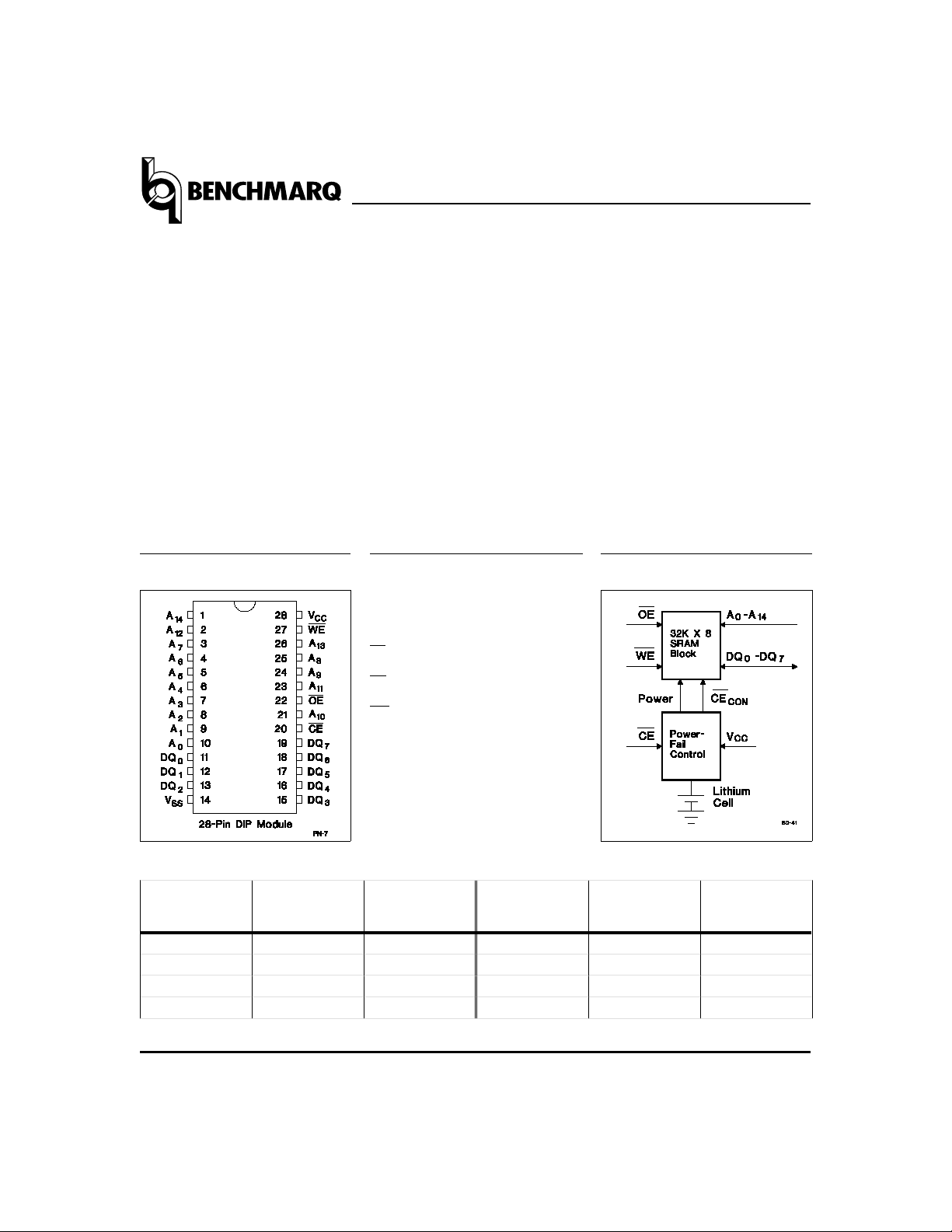
Pin Names
A0 –A
DQ
0
CE Chip enable input
OE Output enable input
WE Write enable input
Address inputs
14
–DQ7Data input/output
At this time the integral energy
source is switched on to sustain the
memory until after V
The bq4011 uses an extremely low
standby current CMOS SRAM,
coupled with a small lithium coin cell
to provide nonvolatility without long
write-cycle times and the write-cycle
limitations associated with EEPROM.
The bq4011 requires no external circuitry and is socket-compatible with
industry-standard SRAMs and most
EPROMs and EEPROMs.
returns valid.
CC
Block DiagramPin Connections
Selection Guide
Part
Number
bq4011 -100
bq4011 -150
bq4011 -200
Aug. 1993 C
V
CC
V
SS
Maximum
Access
Time (ns)
100 -5%
150 -5%
200 -5%
+5 volt supply input
Ground
Negative
Supply
Tolerance
Part
Number
bq4011Y-70
bq4011 Y -100
bq4011 Y -150
bq4011 Y -200
1
Maximum
Access
Time ( ns)
70 -10%
100 -10%
150 -10%
200 -10%
Negative
Supply
Tolerance

bq4011/bq4011Y
Functional Description
When power is valid, the bq4011 operates as a standard
CMOS SRAM. During power-down and power-up cycles,
the bq4 011 ac ts as a no nvolati le memo ry, automa tically
protecting and preserving the memory contents.
Power-down/power-up control circuitry constantly
monit ors t he V
. The bq4011 monitors for V
V
PFD
use in system s with 5% supply tole rance. The bq4011 Y
monitors f or V
10% supply tolerance.
When V
CC
automatically write-protects the data. All outputs
become high impedance, and all inputs are treated as
“don’t care.” If a valid access is in process at the time of
power-fail detection, the memory cycle continues to completion. If the memory cycle fails to terminate within
time t
WPT
supply for a power-fail-detect threshold
CC
= 4.37V typical for use in systems with
PFD
falls below the V
= 4.62V typical for
PFD
threshold, the SRAM
PFD
, write-protection takes place.
falls past V
As V
CC
circuitry switches to the internal lithium backup supply,
which provides data retention until valid V
When V
retur ns to a level abov e the interna l backup
CC
cell voltage, the supply is switched back to V
ramps above the V
V
CC
continues for a time t
processor stabilization. Normal memory operation may
resume aft er this time.
The internal coin cell used by the bq4011 has an
extrem ely lon g shel f life and prov ides da ta rete ntion f or
more than 10 years in the absence of system power.
As shipped from Benchmarq, the integral lithium cell is
electr icall y isol ated from t he mem ory. ( Self- disch arge i n
this condition is approximately 0.5% per year.) Following
the first application of V
the lithium backup cell provides data retention on subsequent power-downs.
and approaches 3V, the control
PFD
is applied.
CC
threshold, write-protection
PFD
(120ms maxi mum) t o al low for
CER
, thi s is ol ation is br oken, a nd
CC
Truth Tab le
Mode CE WE OE I/O Operation Power
Not selected H X X High Z Standby
Output disable L H H High Z Active
Read L H L D
Write LLX D
OUT
IN
Active
Active
CC.
After
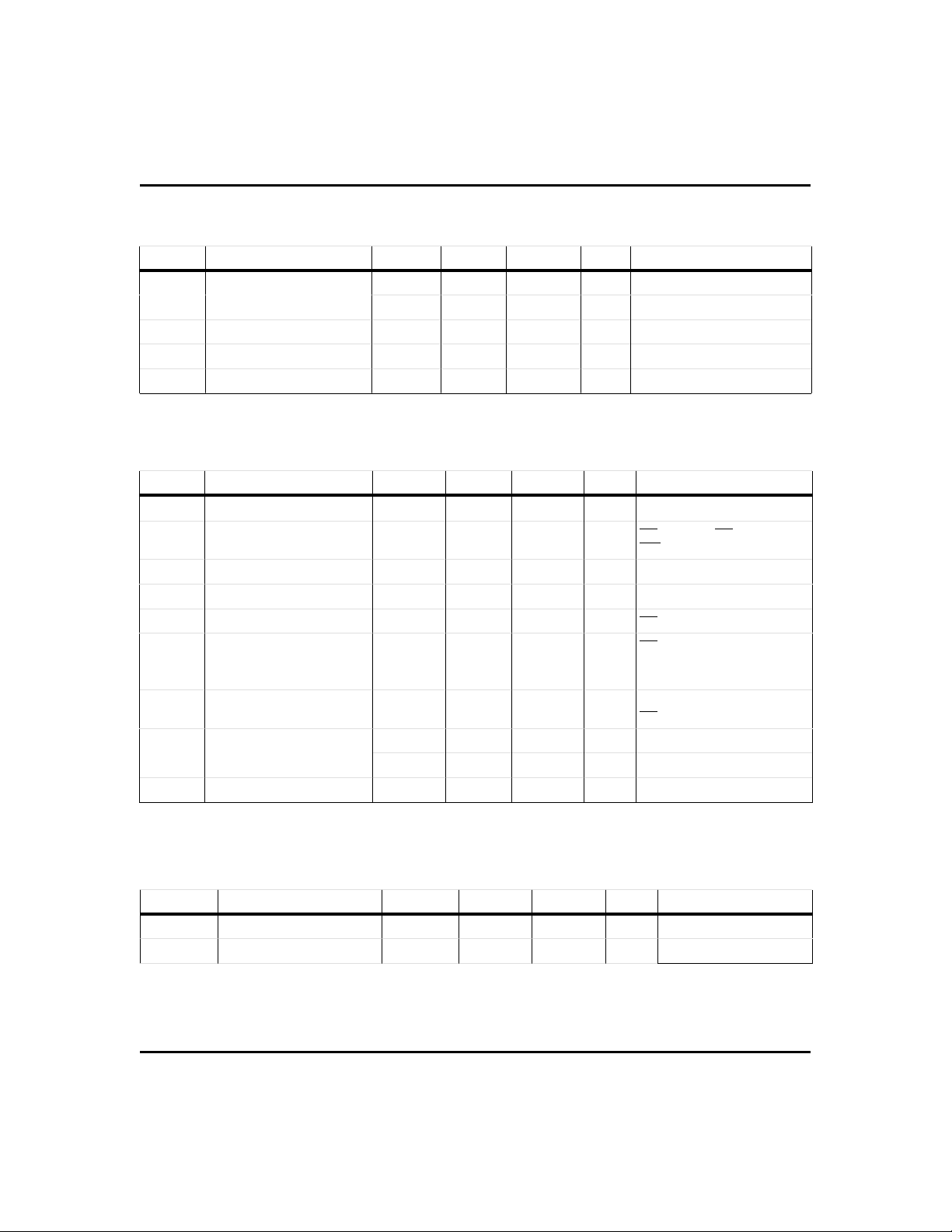
Absolute Maximum Ratings
Symbol Parameter Value Unit Conditions
V
CC
V
T
T
OPR
T
STG
T
BIAS
T
SOLDER
Note: Permanent device damage may occ ur if Absolute Maximum Ratings are exceeded. Functional operation
DC voltage applied on VCC relative to V
SS
DC voltage applied on any pin excluding V
relative to V
SS
CC
-0.3 to 7.0 V
-0.3 to 7.0 V
V
≤ VCC + 0.3
T
0 to +70 °C Commerc ial
Operati ng temperature
-40 to +85 °C Industrial “N”
-40 to +70 °C Commercial
Storage temperature
-40 to +85 °C Industrial “N”
-10 to +70 °C Commercial
Temper atur e unde r bi as
-40 to +85 °C Industrial “N”
Soldering temperature +260 °C For 10 se c onds
should be limited to the Recommended DC Operating Conditions detailed in this data sheet. Exposure to
conditions beyond the operational limits for extended periods of time may affect device reliability.
Aug. 1993 C
2

bq4011/bq4011Y
Recommended DC Operating Conditions (T
A
= T
OPR
)
Symbol Parameter Minimum Typica l M ax imum Unit Notes
4.5 5.0 5.5 V bq4011Y/bq4011Y-xxxN
V
V
V
V
Note: Typica l va lues indic ate op e ra tion at T
DC Electrical Characteristics (T
Supply voltage
CC
Supply voltage 0 0 0 V
SS
Input low voltage -0.3 - 0.8 V
IL
Input high voltage 2.2 - VCC + 0.3 V
IH
4.75 5.0 5.5 V bq4011
= 25°C.
A
= T
A
OPR, VCCmin
≤ VCC ≤ V
CCmax)
Symbol Parameter Minimum Typical Maximum Unit Conditions/Notes
I
I
V
V
I
LI
LO
OH
OL
SB1
Input leakage current - -
Output leakage current - -
± 1 µA
± 1 µA
VIN = VSS to V
CE = VIH or OE = VIH or
WE = V
IL
Output high voltage 2.4 - - V IOH = -1.0 mA
Output low voltage - - 0.4 V IOL = 2.1 mA
Standby supply current - 4 7 mA CE = V
IH
CC
CE ≥ VCC - 0.2V,
I
I
SB2
CC
Standby supply current - 2.5 4 mA
Operating supply current - 55 75 mA
0V ≤ V
or V
≤ 0.2V,
IN
≥ VCC - 0.2V
IN
Min. cycle, duty = 100%,
CE = VIL, I
= 0mA
I/O
4.55 4.62 4.75 V bq4011
V
PFD
V
SO
Power-fail-detect voltage
4.30 4.37 4.50 V bq4011Y
Supply switch-over voltage - 3 - V
Note: Typi ca l values indic at e ope ra t io n at T
Capacitance (T
= 25°C, F = 1MHz, VCC = 5.0V)
A
= 25°C, VCC = 5V.
A
Symbol Parameter Minimum Typical Maximum Unit Conditions
C
I/O
C
IN
Input/output capacitance - - 10 pF Output voltage = 0V
Input capacitance - - 10 pF Input voltage = 0V
Note: These parameters are sampled and not 100% tested.
Aug. 1993 C
3

bq4011/bq4011Y
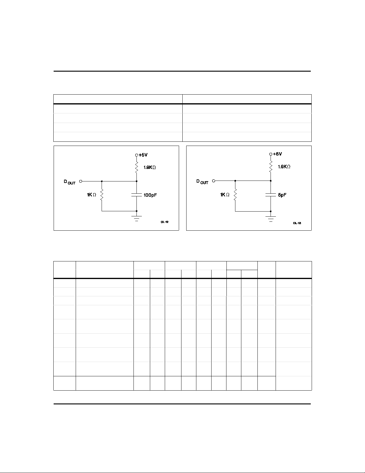
AC Test Conditions
Parameter Test Conditions
Input pulse levels 0V to 3.0V
Input rise and fall times 5 ns
Input and output timing reference levels 1.5 V (unless otherwise specified)
Output load (including scope and jig) See Figures 1 and 2
Figure 1. Output Load A Figure 2. Output Load B
Read Cycle (T
A
= T
Symbol Parameter
t
RC
t
AA
t
ACE
t
OE
t
CLZ
t
OLZ
t
CHZ
t
OHZ
t
OH
Read cycle time 70 - 100 - 150 - 200 - ns
Address access time - 70 - 100 - 150 - 200 ns Output load A
Chip enable access time - 70 - 100 - 150 - 200 ns Output load A
Output enable to
output valid
Chip enable to output
in low Z
Output enable to
output in low Z
Chip disable to output
in high Z
Output disable to
output in high Z
Output hold from
address change
OPR
, V
CCmin
≤ VCC ≤ V
CCmax
)
-70/-70N -100 -150/-150N -200
Min. Max. Min. Max. Min. Max.
- 35 - 50 - 70 - 90 ns Output load A
5 - 5 - 10 - 10 - ns Output load B
5 - 5 - 5 - 5 - ns Output load B
025040060070nsOutput load B
025035050070nsOutput load B
10 - 10 - 10 - 10 - ns Output load A
4
Min. Max.
Unit Conditions
Aug. 1993 C
 Loading...