

Texas Instruments BQ4010MA-70, BQ4010MA-200, BQ4010MA-150, BQ4010YMA-85N, BQ4010YMA-85 Datasheet
...
bq4010/bq4010Y
8Kx8 Nonvolatile SRAM
Features
➤ Data retention in the absence of
power
➤ Automatic write-pro tection
during power-up/power-down
cycles
➤ Industry-standard 28-pin 8K x 8
pinout
➤ Conventional SRAM operation;
unlimited write cycles
➤ 10-year minimum data retention
in absence of power
➤ Battery internally isolated until
power is applied
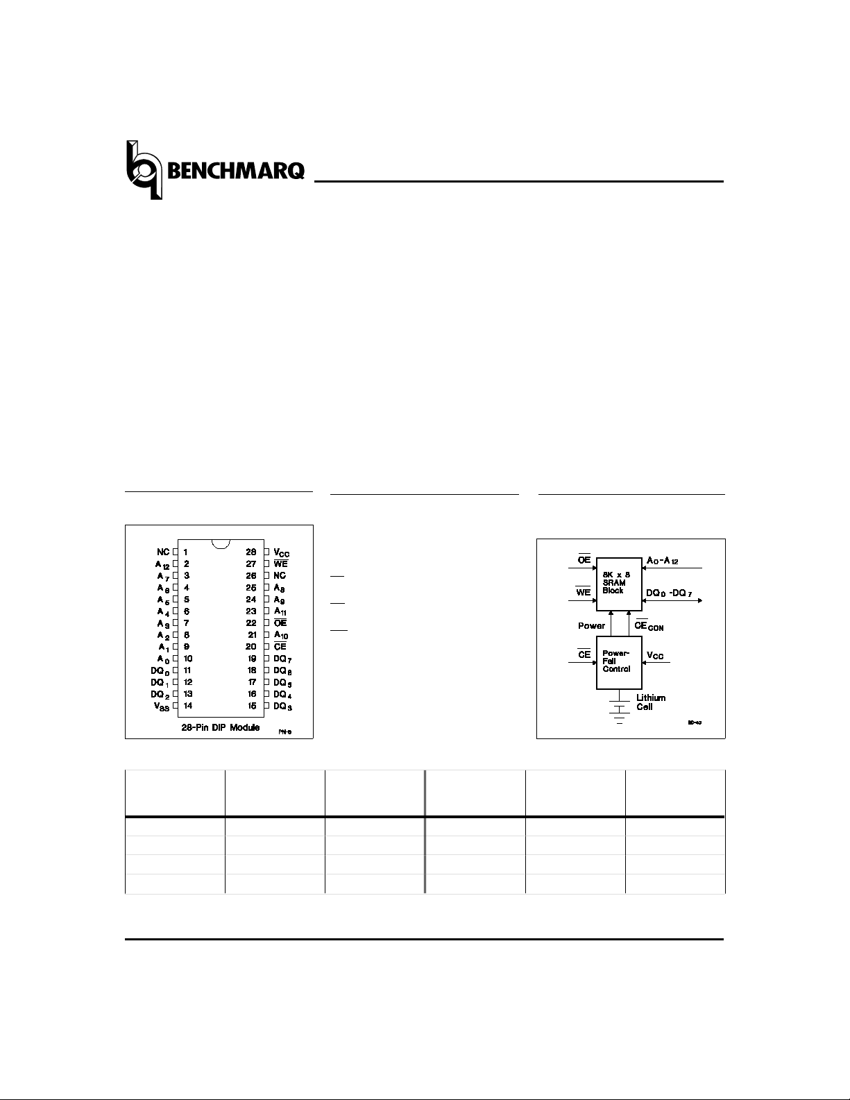
Pin Connections
General Description
The CMOS bq4010 is a nonvolatile
65,536-bit static RAM organized as
8,192 words by 8 bits. The integral
control circuitry and lithium energy
source provide reliable nonvolatility
coupled with the unlimited write
cycles of standard SRAM.
The control circuitry constantly
monitors the single 5V supply for an
out-of-tolerance condition. When V
falls out of tolerance, the SRAM is
unconditionally write-protected to
prevent inadvertent write operation.
CC
Pin Names
A0 –A
DQ
0
CE Chip enable input
OE Output enable input
WE Write enable input
Address inputs
12
–DQ7Data input/output
At this time the integral energy
source is switched on to sustain the
memory until af ter V
The bq4010 uses an extremely low
standby current CMOS SRAM,
coupled with a small lithium coin
cell to provide nonvolatility without
long write-cycle times and the writecycle limitations associated with
EEPROM.
The bq4010 re quires no exter nal circuitry and is sock et-com patible wit h
industry-standard SRAMs and most
EPROMs and EEPROMs.
returns valid.
CC
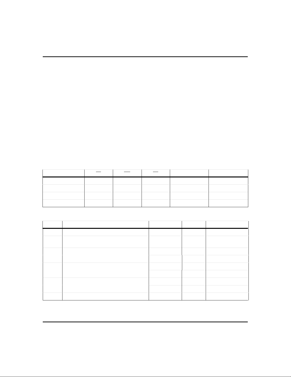
Block Diagram
Selection Guide
Part
Number
bq4010 -85
bq4010 -150
bq4010 -200
Sept. 1996 D
NC No connect
V
CC
V
SS
Maximum
Access
Time (ns)
85 -5%
150 -5%
200 -5%
+5 volt supply input
Ground
Negative
Supply
Tolerance
Part
Number
bq4010 Y -70
bq4010 Y -85
bq4010 Y -150
bq4010 Y -200
1
Maximum
Access
Time (ns)
70 -10%
85 -10%
150 -10%
200 -10%
Negative
Supply
Tolerance
bq4010/bq4010Y
Functional Descri ption
When p ower is val id, the bq4010 o perates as a standard
CMOS SRAM. During power-down and power-up cycles,
the bq4010 acts as a nonvo latile memor y, automatically
protecting and preserving the memory contents.
Power-down/power-up control circuitry constantly
monitor s the V
. The bq4010 monitors for V
V
PFD
use in syst ems with 5% suppl y tolerance. Th e bq4010Y
monitors f or V
10% supply tolerance.
When V
CC
automatically write-protects the data. All outputs
become high impedance, and all inputs are treated as
“don’t care.” If a valid access is in process at the time of
power-fail detection, the memory cycle continues to completion. If the memory cycle fails to terminate within
time t
WPT
supply for a power-fail-detect threshold
CC
= 4.37V typi cal for use in systems with
PFD
falls below the V
= 4.62V typic al for
PFD
threshold, the SRAM
PFD
, write-protection takes place.
falls past V
As V
CC
circuitry switches to the internal lithium backup supply,
which provides data retention until valid V
When V
returns to a level above the internal backup
CC
cell voltage, the supply is switched back to V
ramps above the V
V
CC
continues for a time t
processor stabilization. Normal memory operation may
resume after this time.
The internal coin cell used by the bq4010 has an
extrem ely long shel f life and prov ides data reten tion for
more than 10 years in the absence of system power.
As shipped from Benchmar q, the integral lithium cell is
electr ically isola ted from th e memory . (Self-dis charge in
this con di ti on is approx ima te ly 0.5 % p e r ye ar .) Foll ow in g
the first application of V
the lithium backup cell provides data retention on
subsequent power-downs.
and approaches 3V, the co ntrol
PFD
is applied.
CC
threshold, write-protection
PFD
(120ms m aximu m) to allo w f or
CER
, this iso lation is broken , and
CC
Truth Table
Mode CE WE OE I/O Operatio n Power
Not selected H X X High Z Standby
Output disable L H H High Z Active
Read L H L D
Write LLX D
OUT
IN
Active
Active
CC
. After
Absolute Maximum Ratings
Symbol Parameter Value Unit Conditions
V
CC
V
T
T
OPR
T
STG
T
BIAS
T
SOLDER
Note: Permanent device damage may occur if Absolute Maxi mum Ratings are exceeded. F unctional operation
DC voltage applied on VCC relative to V
SS
DC voltage applied on any pin excluding V
relative to V
SS
CC
-0.3 to 7.0 V
-0.3 to 7.0 V
V
≤ VCC + 0.3
T
0 to +70 °C Commercial
Operat ing temperature
-40 to +85 °C Industrial “N”
-40 to +70 °C Commercial
Storage temperature
-40 to +85 °C Industrial “N”
-10 to +70 °C Commercial
Temperature under bias
-40 to +85 °C Industrial “N”
Soldering temperature +260 °C For 10 seconds
should be limited to the Recommended DC Operating Conditions detailed in this data sheet. Exposure to conditions beyond the operational limits for extended periods of time may affect device reliability.
Sept. 1996 D
6-2
bq4010/bq4010Y
Recommended DC Operating Conditions (T
A
= T
OPR
)
Symbol Parameter Minimum Typical Maximum Unit Notes
4.5 5.0 5.5 V bq4010Y/bq4010Y-xxxN
V
V
V
Note: Typical values indicate operation at T
DC Electrical Characteristics (T
Supply voltage
CC
Supply voltage 0 0 0 V
SS
Input low voltage -0.3 - 0.8 V
V
IL
Input high voltage 2.2 - VCC + 0.3 V
IH
4.75 5.0 5.5 V bq4010
= 25°C.
A
A
= T
OPR
, V
CCmin
≤ VCC ≤ V
CCmax)
Symbol Parameter Minimum Typical Maximum Unit Conditions/Notes
I
I
V
V
I
LI
LO
OH
OL
SB1
Input leakage current - -
Output leakage current - -
± 1 µA
± 1 µA
VIN = VSS to V
CE = VIH or OE = VIH or
WE = V
IL
Output high voltage 2.4 - - V IOH = -1.0 mA
Output low voltage - - 0.4 V IOL = 2.1 mA
Standby supply current - 4 7 mA CE = V
IH
CC
CE ≥ VCC - 0.2V,
I
I
SB2
CC
Standby supply current - 2.5 4 mA
Operating supply current - 65 75 mA
0V ≤ V
or V
≤ 0.2V,
IN
≥ VCC - 0.2V
IN
Min. cycle, duty = 100%,
CE = VIL, I
= 0mA
I/O
4.55 4.62 4.75 V bq4010
V
PFD
V
SO
Power-fail-detect voltage
4.30 4.37 4.50 V bq4010Y
Supply switch-over vol t age - 3 - V
Note: Typical values indicate operation at T
Capacitance (T
= 25°C, F = 1MHz, VCC = 5.0V)
A
= 25°C, VCC = 5V.
A
Symbol Parameter Minimum Typical Maximum Unit Conditions
C
I/O
C
IN
Input/output capacitance - - 10 pF Output voltage = 0V
Input capacitance - - 10 pF Input voltage = 0V
Note: These parameters are sampled and not 100% tested.
Sept. 1996 D
6-3

bq4010/bq4010Y
AC Test Conditions
Parameter Test Conditions
Input pulse levels 0V to 3.0V
Input rise and fall times 5 ns
Input and output timing reference levels 1.5 V (unless otherwise specified)
Output load (including scope and jig) See Figures 1 and 2
Figure 1. Output Load A Figure 2. Output Load B
Read Cycle (T
Symbol Parameter
t
RC
t
AA
t
ACE
t
OE
t
CLZ
t
OLZ
t
CHZ
t
OHZ
t
OH
Read cycle time 70 - 85 - 150 - 200 - ns
Address access time - 70 - 85 - 150 - 200 ns Output load A
Chip enable access time - 70 - 85 - 150 - 200 ns Output load A
Output enable to output
valid
Chip enable to output
in low Z
Output enable to output
in low Z
Chip disable to output
in high Z
Output disable to
output in high Z
Output hold from
address change
A
= T
OPR
, V
CCmin
≤ V
CC
≤ V
CCmax
)
-70/-70N -85/-85N -150/-150N -200
Min. Max. Min. Max. Min. Max.
Min. Max.
Unit Conditions
- 35 - 45 - 70 - 90 ns Output load A
5-5-10-10-nsOutput load B
5-5-5-5-nsOutput load B
025040060070nsOutput load B
025030050070nsOutput load B
10 - 10 - 10 - 10 - ns Output load A
Sept. 1996 D
6-4

bq4010/bq4010Y
Read Cycle No. 1 (Address Access)
Read Cycle No. 2 (CE Access)
Read Cycle No. 3 (OE Access)
1,3,4
1,5
1,2
Notes: 1. WE is held high for a read cycle.
2. Device is continuously selected:
3. Address is valid prior to or coincident with
4.
OE = VIL.
Sept. 1996 D
5. Device is continuously selected:
CE = OE = VIL.
CE transition low.
CE = VIL.
6-5

bq4010/bq4010Y
Write Cycle (T
A
Symbol Parameter
t
t
t
t
t
t
t
t
t
t
t
t
WC
CW
AW
AS
WP
WR1
WR2
DW
DH1
DH2
WZ
OW
Write cycle time 70 - 85 - 150 - 200 - ns
Chip enable to end
of writ e
Address valid to end
of writ e
Address setup time0-0-0-0-ns
Write pulse width 55 - 65 - 90 - 130 - ns
Write recovery time
(write cycle 1)
Write recovery time
(write cycle 2)
Data valid to end of
write
Data hold time
(write cycle 1)
Data hold time
(write cycle 2)
Write enabled to
output in high Z
Output active from
end of wr ite
= T
OPR
, V
CCmin
≤ VCC ≤ V
CCmax
)
-70/-70N -85/-85N -150/-150N -200
Min. Max. Min. Max. Min. Max. Min. Max.
Units Conditions/Notes
55 - 75 - 100 - 150 - ns (1)
55 - 75 - 90 - 150 - ns (1)
5-5-5-5-ns
15 - 15 - 15 - 15 - ns
30 - 35 - 50 - 70 - ns
0-0-0-0-ns
10 - 10 - 0 - 0 - ns
025030050070ns
5-5-5-5-ns
Measured from
address valid to
beginning of write. (2)
Measured from
beginning of write to
end of write. (1)
Measured from
WE
going high to end of
write cycle. (3)
Measured from
CE
going high to end of
write cycle. (3)
Measured from first
low-to-high transition
of either
Measured from
CE or WE.
WE
going high to end of
write cycle. (4)
Measured from
CE
going high to end of
write cycle. (4)
I/O pins are in output
state. (5)
I/O pins are in output
state. (5)
Notes: 1. A write ends at the earlier transition of
2. A write occurs during the overlap of a low
CE going low and WE going low.
of
3. Either t
4. Either t
5. If
CE goes low simultaneously with WE going low or after WE going low, the outputs remain in
WR1
DH1
or t
or t
must be met.
WR2
must be met.
DH2
high-impedance state.
CE going high and WE going high.
CE and a low WE. A write begins at the later transition
Sept. 1996 D
6-6

bq4010/bq4010Y
Write Cycle No. 1 (WE-Controlled)
Write Cycle No. 2 (CE-Controlled)
1,2,3
1,2,3,4,5
Notes: 1. CE or WE must be high during address transition.
Sept. 1996 D
2. Because I/O may be active (
outputs must not be applied.
OE is high, the I/O pins remain in a state of high impedance.
3. If
4. Either t
5. Either t
WR1
DH1
or t
or t
WR2
must be met.
DH2
OE low) during this period, data input signals of opposite po lari ty to the
must be met.
6-7

bq4010/bq4010Y
Power-Down/Power-Up Cycle (T
A
= T
OPR
)
Symbol Parameter Min. Typ. Max. Unit Conditions
t
PF
t
FS
t
PU
VCC slew, 4.75 to 4.25 V 300 - VCC slew, 4.25 to V
VCC slew, VSO to V
SO
(max.) 0 - -
PFD
10 - -
µs
µs
µs
Time during which SRAM is
t
CER
t
DR
t
DR-N
t
WPT
Chip enable recovery time 40 80 120 ms
Data-retention time in
absence of V
CC
Data-retention time in
absence of V
CC
10 - - years TA = 25°C. (2)
6--years
Write-protect time 40 100 150
write-protected after VCC passes
on power-up.
V
PFD
T
= 25°C (2); industrial
A
temperature range (-N) only.
µs
Delay afte r V
before SRAM is write-
V
PFD
slews down past
CC
protected.
Notes: 1. Typical values indicate operation at T
2. Battery is disconnected from circuit until after V
= 25°C, VCC = 5V.
A
is applied for the first time. tDR is the
CC
accumulated time in absence of power beginning when power is first applied to the device.
Caution: Negative undershoots below the absolute maximum rating of -0.3V in battery-backup mode
may affect data integrity.
Power-Down/Power-Up Timing
6-8
Sept. 1996 D

bq4010/bq4010Y
Data Sheet Revision History
Change No. Page No. Descri ption
1 2, 3, 4, 6, 8, 9 Added industrial temperature range for bq4010YMA-85N and -150N.
2 1, 4, 6, 9
3 1 Removed 70ns speed grade for bq4010-70.
Notes: Change 1 = Sept 1991 B changes from Sept. 1990 A.
Change 2 = Feb. 1994 C changes from Sept. 1991 B.
Change 3 = Sept. 1996 D changes from Feb. 1994 C.
MA: 28-Pin A-Type Module
Added 70 ns speed grade for bq4010-70 and bq4010Y-70 and added
industrial temperature range for bq4010YMA-70N.
Sept. 1996 D
28-Pin MA (A-Type Module
Inches Millimeters
Dimension
A 0 .365 0.375 9.27 9.53
A1 0.015 - 0.38 -
B 0 .017 0.023 0.43 0.58
C 0 .008 0.013 0.20 0.33
D 1.470 1.500 37.34 38.10
E 0.710 0.740 18.03 18.80
e 0.590 0.630 14.99 16.00
G 0.090 0.110 2.29 2.79
L 0.120 0.150 3.05 3.81
S 0.075 0.110 1.91 2.79
Min. Max. Min. Max.
)
6-9

bq4010/bq4010Y
Ordering Information
bq4010 MA -
Temperature:
blank = Commercial (0 to +70°C)
N = Industrial (-40 to +85°C)*
Speed Options:
85 = 85 ns
150 = 150 ns
200 = 200 ns
Package Option:
MA = A-type module
Supply Tolerance:
no mark = 5% negative supply tolerance
Y = 10% negative supply tolerance
Device:
bq4010 8K x 8 NVSRAM
*Note: Only 10% supply (“Y”) version is available in industrial
temperature range; contact factory for speed grade
availability.
Sept. 1996 D
6-10

IMPORTANT NOTICE
T exas Instruments and its subsidiaries (TI) reserve the right to make changes to their products or to discontinue
any product or service without notice, and advise customers to obtain the latest version of relevant information
to verify, before placing orders, that information being relied on is current and complete. All products are sold
subject to the terms and conditions of sale supplied at the time of order acknowledgement, including those
pertaining to warranty, patent infringement, and limitation of liability.
TI warrants performance of its semiconductor products to the specifications applicable at the time of sale in
accordance with TI’s standard warranty. Testing and other quality control techniques are utilized to the extent
TI deems necessary to support this warranty . Specific testing of all parameters of each device is not necessarily
performed, except those mandated by government requirements.
CERTAIN APPLICATIONS USING SEMICONDUCTOR PRODUCTS MAY INVOLVE POTENTIAL RISKS OF
DEATH, PERSONAL INJURY, OR SEVERE PROPERTY OR ENVIRONMENTAL DAMAGE (“CRITICAL
APPLICATIONS”). TI SEMICONDUCTOR PRODUCTS ARE NOT DESIGNED, AUTHORIZED, OR
WARRANTED TO BE SUITABLE FOR USE IN LIFE-SUPPORT DEVICES OR SYSTEMS OR OTHER
CRITICAL APPLICA TIONS. INCLUSION OF TI PRODUCTS IN SUCH APPLICATIONS IS UNDERST OOD TO
BE FULLY AT THE CUSTOMER’S RISK.
In order to minimize risks associated with the customer’s applications, adequate design and operating
safeguards must be provided by the customer to minimize inherent or procedural hazards.
TI assumes no liability for applications assistance or customer product design. TI does not warrant or represent
that any license, either express or implied, is granted under any patent right, copyright, mask work right, or other
intellectual property right of TI covering or relating to any combination, machine, or process in which such
semiconductor products or services might be or are used. TI’s publication of information regarding any third
party’s products or services does not constitute TI’s approval, warranty or endorsement thereof.
Copyright 1999, Texas Instruments Incorporated
 Loading...