

Features
➤ Direct clock/calendar replace-
ment for IBM
®
AT-compatible
computers and other applications
➤ Functionally compatible with the
DS1287/DS1287A and MC146818A
➤ 114 bytes of general nonvolatile
storage
➤ Integral lithium cell and crystal
➤ 160 ns cycle time allows fast bus
operation
➤ Selectable Intel or Motorola bus
timing
➤ 14 bytes for clock/calendar and
control
➤ BCD or binary format for clock
and calendar data
➤ Time of day in seconds, minutes,
and hours
-
12- or 24-hour format
- Optional daylight saving
adjustment
➤ Calendar in day of the week, day
of the month, months, and years
with automatic leap-year adjustment
➤ Programmable square wave out-
put
➤ Three individually maskable in-
terrupt event flags:
-
Periodic rates from 122µsto
500 ms
-
Time-of-day alarm once per
second to once per day
-
End-of-clock update cycle
➤ Better than one minute per
month clockaccuracy
General Description
The CMOS bq3287/bq3287A is a
low-power microprocessor peripheral providing a time-of-day clock
and 100-year calendar with alarm
features and battery operation.
Other features include three
maskable interrupt sources, squarewave output, and 114 bytes of general nonvolatile storage. The
bq3287A version is identical to the
bq3287, with the addition of the RAM
clear input.
The bq3287 is a fully compatible
real-time clock for IBM ATcompatible computers and other applications. The bq3287 writeprotects the clock, calendar, and
storage registers during power failure. The integral backup energy
source then maintains data and operates the clockandcalendar.
As shipped from Benchmarq, the
real time clock is turned off to maximize battery capacity for in-system
operation.
The bq3287 is functionally equivalent to the bq3285, except that the
battery (16, 20) and crystal (2, 3)
pins are not accessible. These pins
are connected internally to a coin
cell and quartz crystal. The coin cell
is sized to provide 10 years of data
retention and clock operation in the
absence of power. For a complete description of features, operating conditions, electrical characteristics,
bus timing, and pin descriptions, see
the bq3285 data sheet.
1
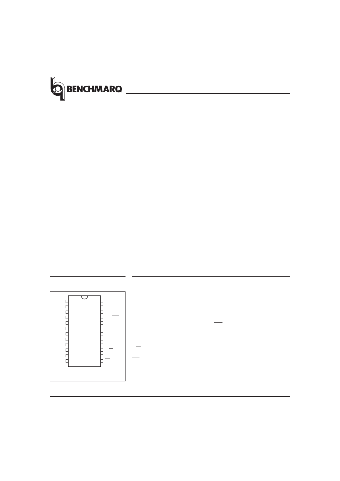
Pin Names
AD0–AD7Multiplexed address/data
input/output
MOT Bus type select input
CS Chip select input
AS Address strobe input
DS Data strobe input
R/W Read/write input
INT Interrupt request output
1
PN328701.eps
24-Pin DIP Module
2
3
4
5
6
7
8
24
23
22
21
20
19
18
17
9
10
16
15
11
12
14
13
V
CC
SQW
NC
NC
INT
RST
DS
NC
R/W
AS
CS
MOT
NC
NC
AD
0
AD
1
AD
2
AD
3
AD
4
AD
5
AD
6
AD
7
V
SS
NC/RCL
Sept. 1996D
RST Reset input
SQW Square wave output
NC No connect
RCL RAM clear input
(bq3287A only)
V
CC
+5V supply
V
SS
Ground
Pin Connections
bq3287/bq3287A
Real-Time Clock(RTC)Module
2
Sept. 1996D
Recommended DC Operating Conditions (T
A=TOPR
)
Symbol Parameter Minimum Typical Maximum Unit
V
CC
Supply voltage 4.5 5.0 5.5 V
V
SS
Supply voltage 0 0 0 V
V
IL
Input low voltage -0.3 - 0.8 V
V
IH
Input high voltage 2.2 - VCC+ 0.3 V
Note: Typical values indicate operation at TA= 25°C.
Absolute Maximum Ratings
Symbol Parameter Value Unit Conditions
V
CC
DC voltage applied on VCCrelative to V
SS
-0.3 to 7.0 V
V
T
DC voltage applied on any pin excluding V
CC
relative to V
SS
-0.3 to 7.0
VV
T
≤
V
CC
+ 0.3
T
OPR
Operating temperature
0 to +70 °C Commercial
-20 to +70 °C Extended “I”
T
STG
Storage temperature
-40 to +70 °C Commercial
-40 to +70 °C Extended “I”
T
BIAS
Temperature under bias
-10 to +70 °C Commercial
-20 to +70 °C Extended “I”
T
SOLDER
Soldering temperature 260 °C For 10 seconds
Note: Permanent device damage may occur if Absolute Maximum Ratings are exceeded. Functional opera-
tion should be limited to the Recommended DC Operating Conditions detailed in this data sheet. Exposure to conditions beyond the operational limits for extended periods of time may affect device reliability.
DC Electrical Characteristics (T
A=TOPR,VCC
=5V±10%)
Symbol Parameter Minimum Typical Maximum Unit Conditions/Notes
I
LI
Input leakage current - -
±
1
µ
AVIN=VSSto V
CC
I
LO
Output leakage current - -
±
1
µ
A
AD0–AD7, INT and SQW
in high impedance
V
OH
Output high voltage 2.4 - - V IOH= -1.0 mA
V
OL
Output low voltage - - 0.4 V IOL= 4.0 mA
I
CC
Operating supply current - 7 15 mA
Min. cycle, duty = 100%,
IOH= 0mA, IOL= 0mA
V
SO
Supply switch-over voltage - 3.0 - V
V
PFD
Power-fail-detectvoltage 4.0 4.17 4.35 V
I
RCL
Input current when RCL =V
SS
- - 185
µ
A
Internal 30K pull-up
(bq3287A only)
I
MOTH
Input current when MOT =
V
CC
- - -185
µ
A Internal 30K pull-down
Note: Typical values indicate operation at TA= 25°C, VCC=5V.
bq3287/bq3287A
3
Sept. 1996D
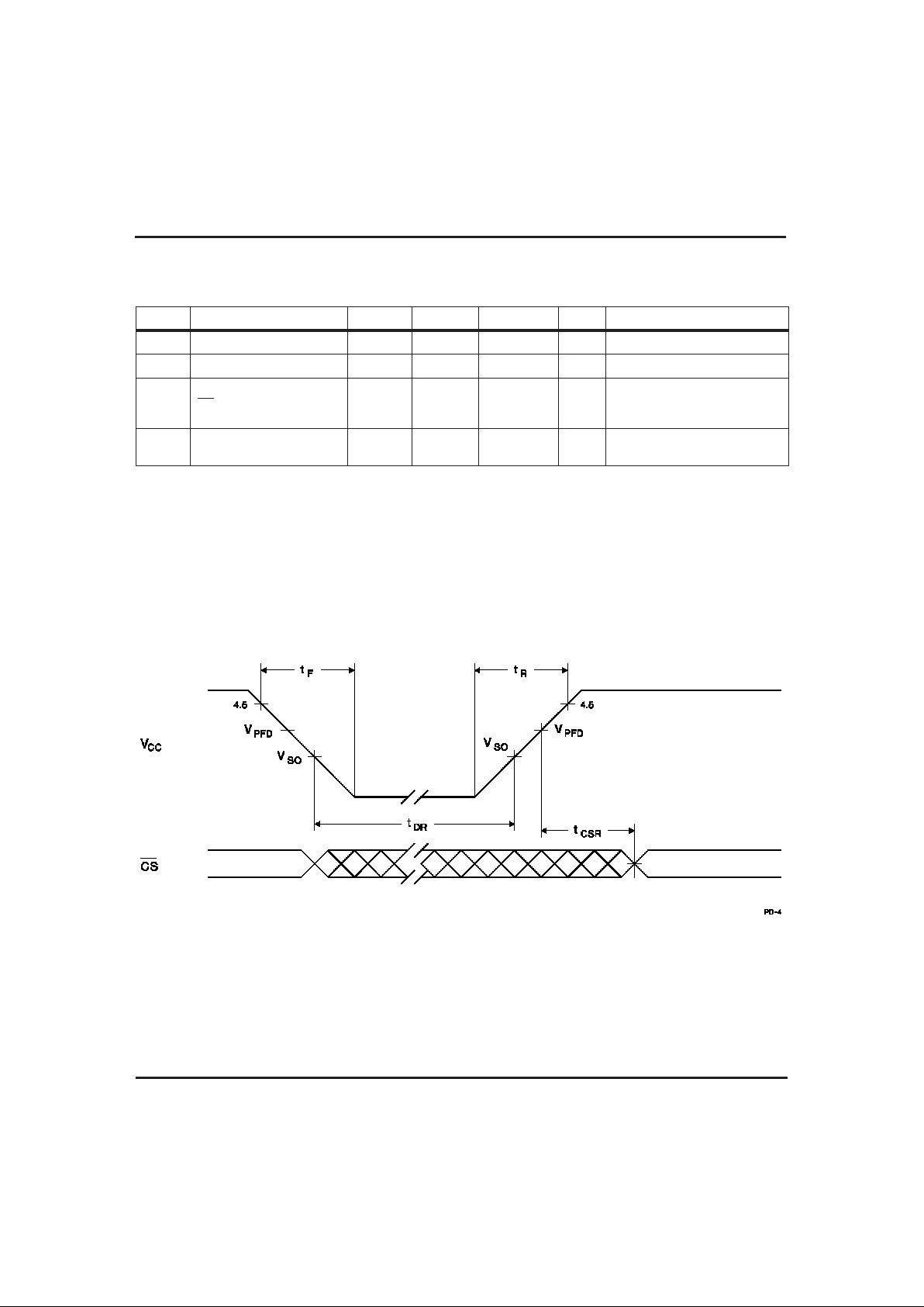
Power-Down/Power-Up Timing (T
A=TOPR)
Symbol Parameter Minimum Typical Maximum Unit Conditions
t
F
VCCslew from 4.5V to 0V 300 - -
µ
s
t
R
VCCslew from 0V to 4.5V 100 - -
µ
s
t
CSR
CS at VIHafter power-up 20 - 200 ms
Internal write-protection
period after VCCpasses V
PFD
on power-up.
t
DR
Data-retention and timekeeping time
10 - - years TA= 25°C.
Note: Clock accuracy is better than±1 minute per month at 25°C for the period of tDR.
Caution: Negative undershoots below the absolute maximum rating of -0.3V in battery-backup mode
may affect data integrity.
Power-Down/Power-Up Timing
bq3287/bq3287A

4
bq3287/bq3287A
Sept. 1996D
24-Pin MT (T-type module)
24-Pin MT (T-type module)
Dimension Minimum Maximum
A 0.360 0.375
A1 0.015 -
B 0.015 0.022
C 0.008 0.013
D 1.320 1.335
E 0.685 0.700
e 0.590 0.620
G 0.090 0.110
L 0.120 0.130
S 0.100 0.120
All dimensions are in inches.

5
Sept. 1996D
bq3287/bq3287A
Ordering Information
Data Sheet Revision History
Change No. Page No. Description Nature of Change
1 1 Address strobe input Clarification
1 2 Power-fail detect voltage V
PFD
Was4.1 min, 4.25 max;
is 4.0 min, 4.35 max
21
Was : “As shipped from Benchmarq,thebackup cell
is electrically isolated from the memory.”
Is: “As shipped from Benchmarq, the backup cell is
electrically isolated from the active circuitry .”
Clarification
22,4
Changed temperature from N (industrial, -40 to
+85°C) to I (extended, -20 to +70°C)
Specification change
32
I
RCL
max. was 275; is now 185. Pull-up = 30K
I
MOTH
max. was -275; is now -185. Pull-down = 30K
Changed values
Notes: Change 1 = Nov. 1992 B changes from June 1991 A.
Change 2 = Nov. 1995 C changes from Nov.1992 B.
Change 3 = Sept. 1996 D changes from Nov.1995 C.
*Contact factory for availability.
bq3287 MT -
PackageOption:
MT = T-type module
Device:
bq3287 Real-Time Clock Module
RAM Clear Option:
A = RAM clear on pin 21
no mark = No connect on pin 21
Temperature:
blank = Commercial (0 to +70°C)
I = Extended* (-20 to +70°C)

IMPORTANT NOTICE
T exas Instruments and its subsidiaries (TI) reserve the right to make changes to their products or to discontinue
any product or service without notice, and advise customers to obtain the latest version of relevant information
to verify, before placing orders, that information being relied on is current and complete. All products are sold
subject to the terms and conditions of sale supplied at the time of order acknowledgement, including those
pertaining to warranty, patent infringement, and limitation of liability.
TI warrants performance of its semiconductor products to the specifications applicable at the time of sale in
accordance with TI’s standard warranty. Testing and other quality control techniques are utilized to the extent
TI deems necessary to support this warranty. Specific testing of all parameters of each device is not necessarily
performed, except those mandated by government requirements.
CERT AIN APPLICATIONS USING SEMICONDUCTOR PRODUCTS MAY INVOLVE POTENTIAL RISKS OF
DEATH, PERSONAL INJURY, OR SEVERE PROPERTY OR ENVIRONMENTAL DAMAGE (“CRITICAL
APPLICATIONS”). TI SEMICONDUCTOR PRODUCTS ARE NOT DESIGNED, AUTHORIZED, OR
WARRANTED TO BE SUITABLE FOR USE IN LIFE-SUPPORT DEVICES OR SYSTEMS OR OTHER
CRITICAL APPLICATIONS. INCLUSION OF TI PRODUCTS IN SUCH APPLICA TIONS IS UNDERSTOOD T O
BE FULLY AT THE CUSTOMER’S RISK.
In order to minimize risks associated with the customer’s applications, adequate design and operating
safeguards must be provided by the customer to minimize inherent or procedural hazards.
TI assumes no liability for applications assistance or customer product design. TI does not warrant or represent
that any license, either express or implied, is granted under any patent right, copyright, mask work right, or other
intellectual property right of TI covering or relating to any combination, machine, or process in which such
semiconductor products or services might be or are used. TI’s publication of information regarding any third
party’s products or services does not constitute TI’s approval, warranty or endorsement thereof.
Copyright 1999, Texas Instruments Incorporated
 Loading...