

Page 1
User's Guide
SLVUB31A–September 2017–Revised March 2018
bq25910EVM-854 Evaluation Module
This user's guide describes the characteristics, operation, and use of the bq25910 Evaluation Module
(EVM). A complete schematic diagram, printed-circuit board layouts, and bill of materials (BOM) are
included in this document.
Contents
1 Introduction ................................................................................................................... 2
1.1 EVM Features....................................................................................................... 2
1.2 I/O Descriptions ..................................................................................................... 2
1.3 Recommended Operating Conditions............................................................................ 4
2 Test Setup and Results ..................................................................................................... 4
2.1 Equipment ........................................................................................................... 4
2.2 Test Setup ........................................................................................................... 5
3 Board Layout ................................................................................................................. 9
4 Schematic and Bill of Materials........................................................................................... 12
4.1 Schematic .......................................................................................................... 12
4.2 Bill of Materials .................................................................................................... 13
List of Figures
1 bq25910EVM-854 Image ................................................................................................... 2
2 bq25910EVM Setup ......................................................................................................... 5
3 bqStudio Device Tabs....................................................................................................... 5
4 bq25910 Registers .......................................................................................................... 6
5 bq25910 WD_RST bit....................................................................................................... 6
6 bq25910 Watchdog Timer Disable ........................................................................................ 7
7 bq25898D Enable HIZ Mode............................................................................................... 7
8 bq25910EVM-854 Top Overlay............................................................................................ 9
9 bq25910EVM-854 Top Solder ............................................................................................. 9
10 bq25910EVM-854 Top Layer .............................................................................................. 9
11 bq25910EVM-854 Signal Layer 1 ......................................................................................... 9
12 bq25910EVM-854 Signal Layer 2 ......................................................................................... 9
13 bq25910EVM-854 Bottom Layer........................................................................................... 9
14 bq25910EVM-854 Bottom Solder ........................................................................................ 10
15 bq25910EVM-854 Bottom Overlay ...................................................................................... 10
16 bq25910EVM-854 Drill Drawing.......................................................................................... 10
17 bq25910EVM-854 Board Dimensions ................................................................................... 10
18 bq25910EVM-854 Schematic............................................................................................. 12
List of Tables
1 Device Data Sheets ......................................................................................................... 2
2 bq25910EVM Ports.......................................................................................................... 3
3 bq25910EVM Jumpers...................................................................................................... 3
4 bq25910EVM Test Points .................................................................................................. 3
5 bq25910EVM Recommended Operating Conditions.................................................................... 4
SLVUB31A–September 2017–Revised March 2018
Submit Documentation Feedback
Copyright © 2017–2018, Texas Instruments Incorporated
bq25910EVM-854 Evaluation Module
1
Page 2
+
-
DC Load
Introduction
6 Bill of Materials ............................................................................................................. 13
1 Introduction
The bq25910 is an integrated three-level switch-mode parallel battery charge management device for
single cell Li-ion and Li-polymer batteries. Utilization of the three-level converter reduces solution footprint
and volume while maintaining highest switch-mode operation efficiency.
This evaluation module includes both the master and parallel chargers: the bq25898D and the bq25910,
respectively. The bq25898D is a highly-integrated 4-A switch-mode battery charge management and
system power-path device for single cell Li-ion and Li-polymer battery.
1.1 EVM Features
The device data sheets, listed in Table 1, provide detailed features and operation.
1.2 I/O Descriptions
The bq25910EVM available ports and jumpers are described in Table 2 and Table 3.
www.ti.com
Table 1. Device Data Sheets
Device Data Sheet
bq25910 SLVSDU0
bq25898D SLUSCA6
NOTE: Do not use sense lines and testpoints on the bq25910EVM to carry large amounts of current.
2
bq25910EVM-854 Evaluation Module
Figure 1. bq25910EVM-854 Image
SLVUB31A–September 2017–Revised March 2018
Copyright © 2017–2018, Texas Instruments Incorporated
Submit Documentation Feedback
Page 3
www.ti.com
Introduction
Table 2. bq25910EVM Ports
Port Description
J1 bq25898D PMID port
J2 bq25898D SYS output
J3 bq25898D and bq25910 VBUS input
J4 Battery connector for both bq25898D and bq25910
J5 I2C Molex connector
J6 bq25910 PMID port
Table 3. bq25910EVM Jumpers
Jumper Description
JP1 Pullup selection jumper. Choose between SYS or BAT. Installed to SYS
JP2 bq25898D battery sense line Installed
JP3 bq25910 INT pin jumper Installed
JP4 bq25898D CE pin (charge enabled) Installed
JP5 bq25898D REGN to TS network connection Installed
JP6 TS network connection to potentiometer Installed
JP7
JP8 bq25898D OTG to GND pin connection Installed
JP9 bq25898D ILIM to GND pin connection Not Installed
JP10 bq25910 IND_SNS pin connection Installed
JP11 bq25910 BATP sense line connection Installed
JP12 bq25910 BATN sense line connection Installed
TS to GND connection. Can also be used to attach an external 103AT
thermistor.
Default
Configuration
Not Installed
Table 4. bq25910EVM Test Points
Test Point Description
VBUS1_s Sense line for the bq25898D VBUS for efficiency measurement
PMID1 Connection to the bq25898D PMID plane
VBUS2_s Sense line for the bq25910 VBUS for efficiency measurement
PMID2 Connection to the bq25910 PMID plane
BAT_s bq25898D battery sense line
BATP bq25910 positive battery sense line
BATN bq25910 negative battery sense line
GND_s bq25910 sense line to GND plane near IC for efficiency measurement
SW1 bq25898D switch node
SW2 bq25910 switch node
VOUT_910_s bq25910 converter output for efficiency measurement
CFLY+/CFLY– Differential test points for the bq25910 CFLY capacitor
CDRV+/CDRV– Differential test points for the bq25910 CDRV capacitor
INT2 bq25910 Interrupt pin
CAUX bq25910 CAUX capacitor
REGN bq25910 REGN output
SLVUB31A–September 2017–Revised March 2018
Submit Documentation Feedback
Copyright © 2017–2018, Texas Instruments Incorporated
bq25910EVM-854 Evaluation Module
3
Page 4
Introduction
1.3 Recommended Operating Conditions
Table 5. bq25910EVM Recommended Operating Conditions
Symbol Description MIN TYP MAX Unit
VBUS Input voltage from AC adapter 3.9 14 V
IBUS Input supply current from AC adapter 3.6 A
VBAT Battery voltage applied at J4 0 4.775 V
IBAT bq25910 output current 0 6 A
2 Test Setup and Results
2.1 Equipment
In order to evaluate the bq25910EVM, the following are required:
• Power Supply: Capable of providing up to 14 V and 3.6 A to be used for VBUS.
• Battery Emulator: A 4-quadrant supply capable of constant voltage ≤ 4.775 V and constant current ≤
6 A.
• DC Electronic Load: Used to emulate system load.
• Multimeters: Used for voltage measuring and at least 2 current meters capable of measuring 6 A or
can use the sense resistors on the board.
• Computer: A computer with at least one USB port and USB cable.
• EV2400 USB-based PC Interface Board: Used to interface with the bq25910EVM via I2C. The
EV2400 is purchased separately and is found here.
• bqStudio: Software platform used to send commands to the bq25910EVM via I2C using the EV2400.
Download the latest version of bqStudio from ti.com. Double click the bqStudio setup installation file
and follow the installation prompts. The software supports Microsoft®Windows®XP and Windows 7
operating systems.
www.ti.com
4
bq25910EVM-854 Evaluation Module
SLVUB31A–September 2017–Revised March 2018
Copyright © 2017–2018, Texas Instruments Incorporated
Submit Documentation Feedback
Page 5
EV2400
USB
Port
I2C
bq25910EVM
+
±
I2C
GND
BAT
J4
VBUS
J3
GND
J5
SYS
J2
GND
Power Supply
Li-ion battery/
battery emulator
DC Load
www.ti.com
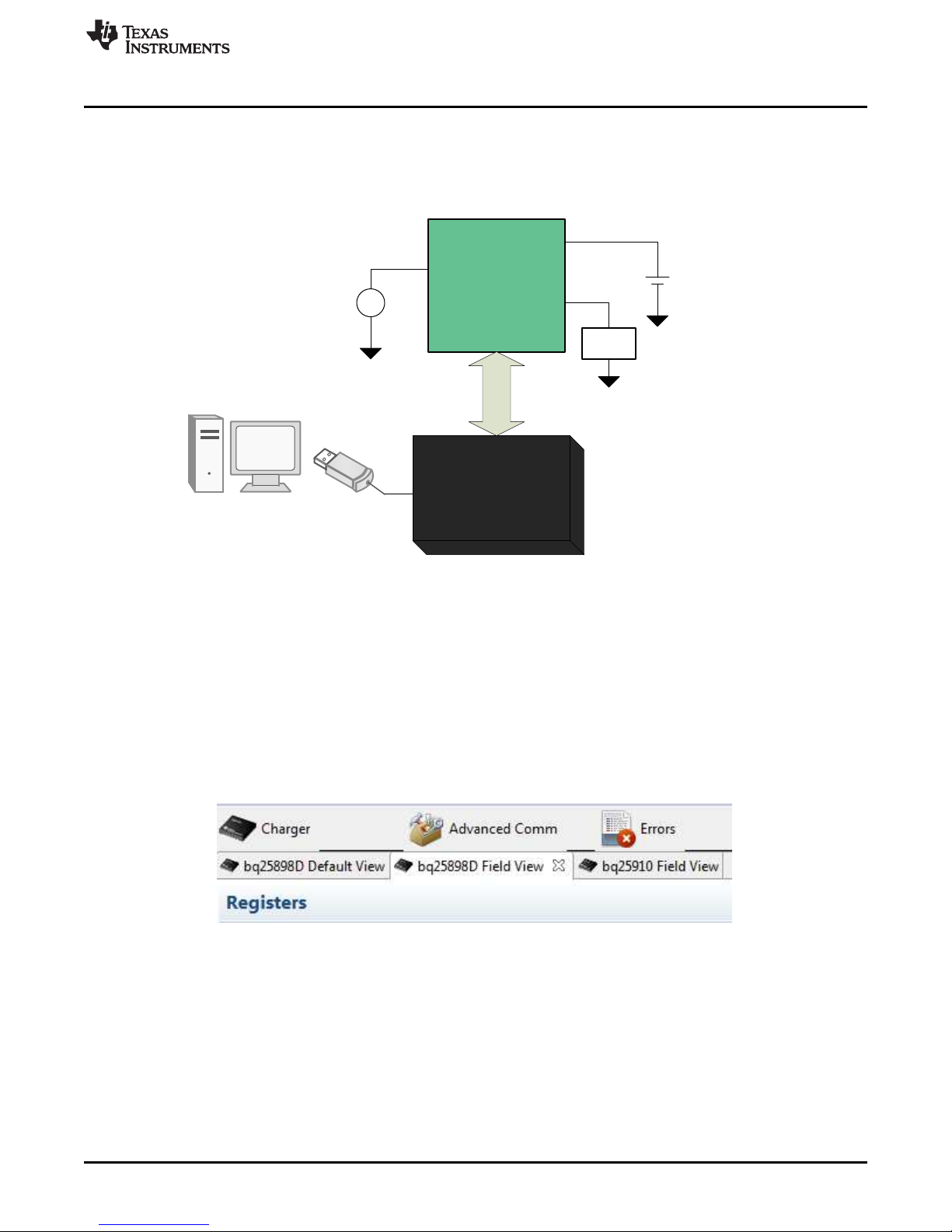
2.2 Test Setup
Both the master and parallel chargers are present on the EVM. This user's guide focuses on setting up
and evaluation of the bq25910 charger.
Figure 2 shows the connections between the power supplies, EV2400 and the bq25910EVM.
Test Setup and Results
2.2.1 Setting up the bq25898D
This user's guide covers the necessary steps to set up the master charger for parallel charger evaluation.
• Connect the battery emulator to battery connector, J4. Set battery emulator to 3.8 V.
• Using a 4-wire Molex cable (included with EV2400), connect the I2C port to the J5 connector on the
EVM. Connect the USB cable to any USB port on the PC with bqStudio installed.
• Apply 5 V at VBUS connector, J3. At this point, the bq25898D should be providing 2 A of charge
current to the battery.
• Open bqStudio and select the bq25910EVM from the Charger menu.
• The software allows you to modify both the bq25898D and bq25910 I2C registers. Figure 3 shows the
device tabs on bqStudio. Selecting one of them opens the register interface for that particular device
and allows the values to be modified via I2C.
• The DC electronic load can be connected at J2 to emulate the system load. Note the 4-A maximum
output current of the converter and the maximum 6 A of continuous discharge current from the battery
of the bq25898D.
• For full details on the test setup of the bq25898D, refer to bq25898, bq25898D, and bq25898C
PWR730 Evaluation Module.
• To evaluate bq25910 only, place the bq25898D in HIZ mode.
Figure 2. bq25910EVM Setup
Figure 3. bqStudio Device Tabs
SLVUB31A–September 2017–Revised March 2018
Submit Documentation Feedback
Copyright © 2017–2018, Texas Instruments Incorporated
bq25910EVM-854 Evaluation Module
5
Page 6
Test Setup and Results
2.2.2 Setting up the bq25910
This section describes the options available for evaluation of the bq25910 and how to set up the device for
basic evaluation.
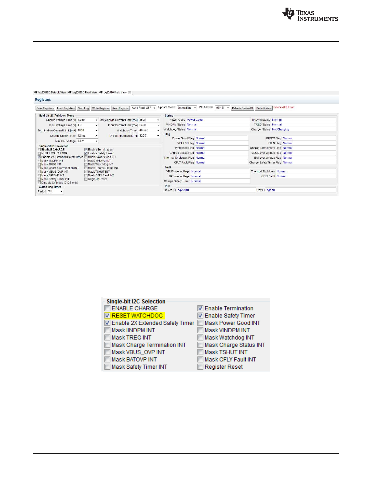
• Once the master charger is set up, select the bq25910 Field View tab on bqStudio to continue to set
up the parallel charger.
www.ti.com
Figure 4. bq25910 Registers
• Figure 4 shows the configurable registers, single-bit I2C commands and status registers available for
the bq25910.
• The bq25910 is a host controlled parallel charger and will automatically shut off when the I2C
watchdog timer is not reset within the timer period (40 seconds by default). While in default mode,
charging is disabled until the host sets the ENABLE CHARGE bit and resets the watchdog timer via
the WD_RST bit (RESET WATCHDOG command).
• After POR, the device is in default mode with the watchdog timer expired. While in default mode, the
bq25910 remains in HIZ mode and will not charge the battery.
• The WD_RST bit needs to be set first to force the charger out of default mode. This can be done by
setting the RESET WATCHDOG checkbox on bqStudio, see Figure 5 for the location of the WD_RST
bit in the Single-bit I2C Selection section of bqStudio.
Figure 5. bq25910 WD_RST bit
• Once WD_RST is set, all the device parameters can be programmed. To keep the device in host
mode, the host has to reset the watchdog timer by setting the WD_RST bit before the timer expires or
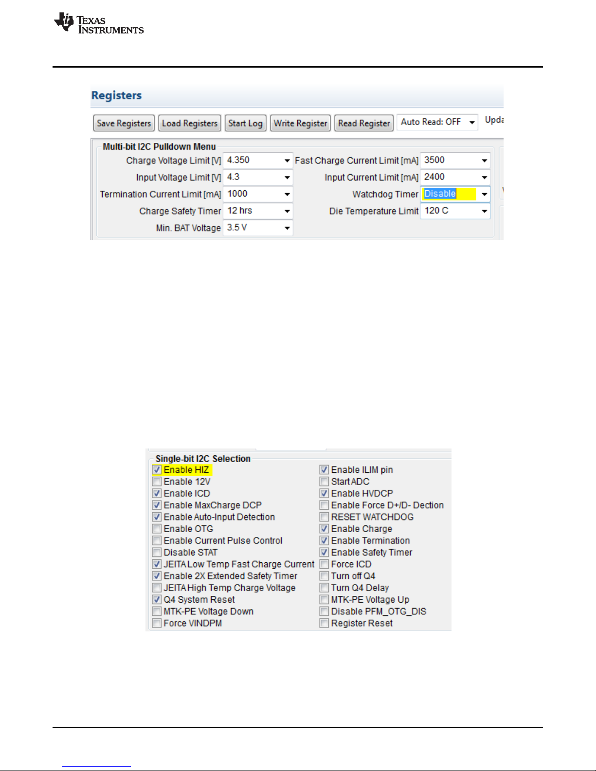
disable the watchdog timer. For the purpose of this evaluation, we disable the watchdog timer by
writing REG05[5:4] = 00b. This can be done by using the drop-down menu for the Watchdog Timer
setting on the Multi-bit I2C Pulldown Menu. See Figure 6 for the location in bqStudio.
6
bq25910EVM-854 Evaluation Module
SLVUB31A–September 2017–Revised March 2018
Copyright © 2017–2018, Texas Instruments Incorporated
Submit Documentation Feedback
Page 7
www.ti.com
Figure 6. bq25910 Watchdog Timer Disable
2.2.3 Master and Parallel Chargers Interaction
The bq25898D acts as the master charger and is in charge of pre-conditioning and full termination of the
battery. The parallel charger, the bq25910, monitors the battery voltage and compares it to the V
threshold. Once the battery voltage rises above the V
charging, applying the charge current set on the Fast Charge Current Limit register.
Once the bq25910 begins charging, the master charger can be either placed in HIZ mode or continue
running in parallel with the bq25910.
BAT_LOWV
Test Setup and Results
BAT_LOWV
threshold, the bq25910 turns on and begins
2.2.3.1 Master Charger In HIZ mode
Placing the master charger in HIZ mode when the parallel charger begins charging is recommended
because this allows evaluating the performance of the bq25910 independently from the master charger.
This can be done by navigating to the bq25898D tab on bqStudio and setting the Enable HIZ checkbox,
refer to Figure 7.
Figure 7. bq25898D Enable HIZ Mode
SLVUB31A–September 2017–Revised March 2018
Submit Documentation Feedback
Copyright © 2017–2018, Texas Instruments Incorporated
bq25910EVM-854 Evaluation Module
7
Page 8

Test Setup and Results
2.2.4 Measuring bq25910 Charge Efficiency
This section details how to evaluate the bq25910 charge efficiency.
1. Apply 9 V on VBUS at the J3 port on the EVM.
2. Apply 3.8 V on BAT at the J4 port on the EVM.
3. Follow the steps in section 2.2.3.1, to place the master charger in HIZ mode.
4. Follow the steps in section 2.2.2, to enable charge on the bq25910.
5. In order to calculate efficiency, the input voltage, battery voltage and charge current must be set
correctly.
• On bqStudio, navigate to the bq25910 device tab and select 3000mA from the Fast Charge
Current Limit drop-down menu.
• Using a multimeter, measure the voltage at the BAT_s testpoint with respect to the GND_s
testpoint and modify the battery emulator voltage until 3.8 V is measured.
• Using a multimeter, measure the voltage at the VBUS2_s testpoint with respect to the GND_s
testpoint and modify the power supply until 9 V is measured.
• At this point, the device should be providing 3 A of charge current. Input current and charge
current can be measured either by an ammeter in series with VBUS and BAT or measuring the
voltage across the sense resistors, R20 and R21, and converting the voltage to current.
• Once input voltage, battery voltage, charge current and input current are measured, efficiency can
be calculated.
www.ti.com
8
bq25910EVM-854 Evaluation Module
SLVUB31A–September 2017–Revised March 2018
Copyright © 2017–2018, Texas Instruments Incorporated
Submit Documentation Feedback
Page 9

www.ti.com
3 Board Layout
Figure 8 through Figure 17 illustrate the bq25910EVM-854 PCB layouts.
Board Layout
Figure 8. bq25910EVM-854 Top Overlay Figure 9. bq25910EVM-854 Top Solder
Figure 10. bq25910EVM-854 Top Layer Figure 11. bq25910EVM-854 Signal Layer 1
SLVUB31A–September 2017–Revised March 2018
Submit Documentation Feedback
Copyright © 2017–2018, Texas Instruments Incorporated
bq25910EVM-854 Evaluation Module
9
Page 10

Board Layout
Figure 12. bq25910EVM-854 Signal Layer 2 Figure 13. bq25910EVM-854 Bottom Layer
www.ti.com
Figure 14. bq25910EVM-854 Bottom Solder Figure 15. bq25910EVM-854 Bottom Overlay
10
bq25910EVM-854 Evaluation Module
SLVUB31A–September 2017–Revised March 2018
Copyright © 2017–2018, Texas Instruments Incorporated
Submit Documentation Feedback
Page 11

www.ti.com
Board Layout
Figure 16. bq25910EVM-854 Drill Drawing Figure 17. bq25910EVM-854 Board Dimensions
SLVUB31A–September 2017–Revised March 2018
Submit Documentation Feedback
Copyright © 2017–2018, Texas Instruments Incorporated
bq25910EVM-854 Evaluation Module
11
Page 12

GND
J3
GND
1µF
C15
10µFC710µF
C6
DNP
10µF
C5
DNP
10µF
C4
DNP
1000pF
C3
DNP
22µF
C2
DNP
GND
J1
GND
1µH
L1
0.047µF
C8
0.047µF
C16
4.7µF
C1
GND
10µFC910µF
C10
10µF
C11
DNP
10µF
C12
DNP
1000pF
C14
DNP
0.1µF
C13
DNP
GND
J2
10µF
C17
J4
GND
1
2
3
JP1
JP2
PULLUP
REGN
SYS
BATSNS
PMID
1
2
3
4
5
TP40
DNP
GND
Green
D1
2.21k
R5
PULLUP
STAT
5.23k
R7
30.1k
R13
JP6
GND
JP7
JP5
REGN
SCL
SDA
10.0kR810.0k
R9
PULLUP
SDA
SCL
10.0k
R10
10.0k
R11
INT
INT
OTG
OTG
JP8
GND
10.0k
R6
GND
JP4
STAT
4.7k
R12
S1
GND
JP9
GND
49.9
R15
10k
R17
768
R16
VBUS
A1
PMID
A2
CFLY+
A3
SW
A4
CFLY-
A5
GND
A6
VBUS
B1
PMID
B2
CFLY+
B3
SW
B4
CFLY-
B5
GND
B6
VBUS
C1
PMID
C2
CFLY+
C3
SW
C4
CFLY-
C5
GND
C6
CDRV+
D1
PMID
D2
CFLY+
D3
SW
D4
CFLY-
D5
GND
D6
CDRV-
E1
SDA
E2
INT
E3
SW
E4
CFLY-
E5
GND
E6
SCL
F1
CAUX
F2
REGN
F3
BATN
F4
BATP
F5
IND_SNS
F6
U2
BQ25910YFFR
VBUS
VBUS
GND
1µF
C18
10µF
C21
GND
PMID1
PMID1
0.22µF
C24
GNDGND
10µF
C22
10µF
C23
GND
BAT
JP11
BATP
BATN
10.0k
R22
PULLUP
SCL
SDA
1
2
3
4
5
TP41
DNP
GND
GND GND
J6
4
1
2
3
J5
GND
SCL
SDA
JP12
TP33
TP8
1
2
3
4
5
TP42
DNP
GND
4.7µF
C26
4.7µF
C25
BATP
220pF
C28
DNP
22µF
C27
DNP
220pF
C29
DNP
22µF
C30
DNP
TP25
TP12
TP11
TP15
TP27 TP28
470nH
L3
DNP
TP3
TP9
TP17
0.01
R20
0.01
R1
0.01
R4
470nH
L2
0.01
R2
0.01
R19
0.01
R18
DNP
0.01
R21
DNP
TP13 TP14
TP22 TP23
TP21
TP24
TP7TP6
TP26
TP32
TP35
TP37
TP36
TP4 TP5
BTST
A6
PGND
G6
SW
F5
PMID
F4
VBUS
E3
SYS
C2
BAT
C1
PGND
C6
DSEL
B5
TS
A4
SCL
A3
VBUS
G3
SYS
E2
BAT
E1
BATSEN
F1
PGND
D6
QON
B6
CE
B4
SDA
B3
SYS
A2
ILIM
G2
PMID
D4
PGND
F6
SW
E5
PMID
E4
D-
D3
SYS
D2
BAT
B1
SW
C5
REGN
A5
SW
G5
PMID
G4
VBUS
F3
INT
F2
BAT
D1
STAT
G1
PGND
E6
SW
D5
OTG
C4
D+
C3
SYS
B2
BAT
A1
U1
BQ25898DYFFR
20
R3
TP1
TP19
TP20
TP16
TP18
TP2
TP34
TP10
TP38
TP29
TP30
TP31
JP3
IND_SNS
PULLUP
GND
50k
R14
TP39
TP43
TP44
JP10
GND
BAT
GND
PMID1
GND
VBUS
GND
PMID2
GND
TP45
TP46
10µF
C31
DNP
10µF
C20
10µF
C19
Copyright © 2018, Texas Instruments Incorporated
Schematic and Bill of Materials
www.ti.com
12
SLVUB31A–September 2017–Revised March 2018
Submit Documentation Feedback
Copyright © 2017–2018, Texas Instruments Incorporated
bq25910EVM-854 Evaluation Module
4 Schematic and Bill of Materials
This section contains the bq25910EVM-854 schematics and bill of materials.
4.1 Schematic
Figure 18 shows the bq25910EVM-854 schematics.
Figure 18. bq25910EVM-854 Schematic
Page 13

www.ti.com
Schematic and Bill of Materials
13
SLVUB31A–September 2017–Revised March 2018
Submit Documentation Feedback
Copyright © 2017–2018, Texas Instruments Incorporated
bq25910EVM-854 Evaluation Module
4.2 Bill of Materials
Table 6 lists the EVM bill of materials.
(1)
Unless otherwise noted in the Alternate Part Number or Alternate Manufacturer columns, all parts may be substituted with equivalents.
Table 6. Bill of Materials
(1)
Designator QTY Value Description Package Reference Part Number Manufacturer Alternate Part Number Alternate
Manufacturer
!PCB 1 Printed Circuit Board PWR854 Any
C1 1 4.7uF CAP, CERM, 4.7 µF, 16 V, +/- 10%, X5R, 0603 0603 GRM188R61C475KAAJ Murata
C7, C9, C10, C17, C21 5 10uF CAP, CERM, 10 µF, 25 V, +/- 20%, X5R, 0603 0603 GRM188R61E106MA73D Murata
C8, C16 2 0.047uF CAP, CERM, 0.047 µF, 25 V, +/- 10%, X7R, 0402 0402 GRM155R71E473KA88D Murata
C15 1 1uF CAP, CERM, 1 µF, 25 V, +/- 10%, X7R, 0805 0805 GRM219R71E105KA88D Murata
C18 1 1uF CAP, CERM, 1 µF, 25 V, +/- 10%, X7R, 0603 0603 GRM188R71E105KA12D Murata
C19, C20 2 10uF CAP, CERM, 10 µF, 10 V, +/- 20%, X5R, 0603 0603 GRM188R61A106MAALD Murata
C22, C23 2 10uF CAP, CERM, 10 µF, 16 V, +/- 20%, X5R, 0603 0603 GRM188R61C106MAALD Murata
C24 1 0.22uF CAP, CERM, 0.22 µF, 6.3 V, +/- 20%, X5R, 0201 0201 GRM033R60J224ME90 Murata
C25, C26 2 4.7uF CAP, CERM, 4.7 µF, 10 V, +/- 20%, X5R, 0402 0402 GRM155R61A475MEAAD Murata
D1 1 Green LED, Green, SMD 1.6x0.8x0.8mm LTST-C190GKT Lite-On
J1, J2, J3, J4, J6 5 Conn Term Block, 2POS, 3.81mm, TH 2POS Terminal Block 1727010 Phoenix Contact
J5 1 Header (friction lock), 100mil, 4x1, R/A, TH 4x1 R/A Header 22-05-3041 Molex
JP1 1 Header, 100mil, 3x1, Tin, TH Header, 3 PIN, 100mil,
Tin
PEC03SAAN Sullins Connector
Solutions
JP2, JP3, JP4, JP5, JP6, JP7,
JP8, JP9, JP10, JP11, JP12
11 Header, 100mil, 2x1, Tin, TH Header, 2 PIN, 100mil,
Tin
PEC02SAAN Sullins Connector
Solutions
L1 1 1uH Inductor, Wirewound, 1 µH, 4 A, 0.041 ohm, SMD 4.06x4.06mm 74437321010 Wurth Elektronik
L2 1 470nH Inductor, Powdered Iron, 470 nH, 5.8 A, 0.017
ohm, SMD
2.5x1.2x2mm DFE252012F-R47M=P2 Murata Toko
R1, R4, R20 3 0.01 RES, 0.01, 1%, 1 W, 2512 2512 WSL2512R0100FEA Vishay-Dale
R2, R19 2 0.01 RES, 0.01, 1%, 1 W, 1206 1206 WSLP1206R0100FEA Vishay-Dale
R3 1 20 RES, 20, 5%, 0.063 W, 0402 0402 CRCW040220R0JNED Vishay-Dale
R5 1 2.21k RES, 2.21 k, 1%, 0.063 W, 0402 0402 CRCW04022K21FKED Vishay-Dale
R6, R8, R9, R10, R11, R22 6 10.0k RES, 10.0 k, 1%, 0.1 W, 0603 0603 RCG060310K0FKEA Vishay Draloric
R7 1 5.23k RES, 5.23 k, 1%, 0.063 W, 0402 0402 CRCW04025K23FKED Vishay-Dale
R12 1 4.7k RES, 4.7k ohm, 5%, 0.063W, 0402 0402 CRCW04024K70JNED Vishay-Dale
R13 1 30.1k RES, 30.1 k, 1%, 0.063 W, 0402 0402 CRCW040230K1FKED Vishay-Dale
R14 1 50k Trimmer, 50k ohm, 0.25W, TH 4.5x8x6.7mm 3266W-1-503LF Bourns
R15 1 49.9 RES, 49.9, 1%, 0.063 W, 0402 0402 CRCW040249R9FKED Vishay-Dale
R16 1 768 RES, 768, 1%, 0.063 W, 0402 0402 CRCW0402768RFKED Vishay-Dale
R17 1 10k Trimmer, 10k ohm, 0.25W, TH 4.5x8x6.7mm 3266W-1-103LF Bourns
S1 1 Switch, Normally open, 2.3N force, 200k
operations, SMD
KSR KSR221GLFS C and K Components
SH-J2, SH-J3, SH-J4, SH-J5,
SH-J8, SH-J9, SH-J10, SHJ11, SH-J12, SH-J14
10 1x2 Shunt, 100mil, Gold plated, Black Shunt SNT-100-BK-G Samtec 969102-0000-DA 3M
Page 14

Schematic and Bill of Materials
www.ti.com
14
SLVUB31A–September 2017–Revised March 2018
Submit Documentation Feedback
Copyright © 2017–2018, Texas Instruments Incorporated
bq25910EVM-854 Evaluation Module
Table 6. Bill of Materials
(1)
(continued)
Designator QTY Value Description Package Reference Part Number Manufacturer Alternate Part Number Alternate
Manufacturer
TP1, TP8, TP12, TP25, TP26,
TP29, TP45
7 Test Point, Miniature, Red, TH Red Miniature Testpoint 5000 Keystone
TP2, TP10, TP34, TP38 4 Test Point, Compact, SMT Testpoint_Keystone_Co
mpact
5016 Keystone
TP3 1 Test Point, Compact, Yellow, TH Yellow Compact
Testpoint
5009 Keystone
TP4, TP5, TP6, TP7, TP13,
TP14, TP16, TP17, TP18,
TP19, TP20, TP21, TP22,
TP23, TP24, TP27, TP28,
TP30, TP31, TP32, TP33,
TP35, TP36, TP37, TP39,
TP43, TP44
27 Test Point, Miniature, White, TH White Miniature Testpoint 5002 Keystone
TP9, TP11, TP15, TP46 4 Test Point, Miniature, Black, TH Black Miniature Testpoint 5001 Keystone
U1 1 I2C Controlled Single Cell 4-A Fast Charger with
MaxCharge Technology, YFF0042AHAC (DSBGA-
42)
YFF0042AHAC BQ25898DYFFR Texas Instruments BQ25898DYFFT Texas Instruments
U2 1 1S, 6A, Three-Level Single-Cell Parallel Charger,
YFF0036AEAE (DSBGA-36)
YFF0036AEAE BQ25910YFFR Texas Instruments BQ25910YFFT Texas Instruments
C2, C27, C30 0 22uF CAP, CERM, 22 µF, 25 V, +/- 20%, X5R, 0805 0805 GRM21BR61E226ME44L Murata
C3, C14 0 1000pF CAP, CERM, 1000 pF, 25 V, +/- 10%, X7R, 0805 0805 GRM216R71E102KA01D Murata
C4, C5, C6, C11, C12 0 10uF CAP, CERM, 10 µF, 25 V, +/- 20%, X5R, 0603 0603 GRM188R61E106MA73D Murata
C13 0 0.1uF CAP, CERM, 0.1 µF, 25 V, +/- 10%, X7R, 0805 0805 GRM21BR71E104KA01L Murata
C28, C29 0 220pF CAP, CERM, 220 pF, 50 V, +/- 1%, C0G/NP0,
0402
0402 C1005C0G1H221F050BA TDK
C31 0 10uF CAP, CERM, 10 µF, 16 V, +/- 20%, X5R, 0603 0603 GRM188R61C106MAALD Murata
FID1, FID2, FID3 0 Fiducial mark. There is nothing to buy or mount. Fiducial N/A N/A
L3 0 470nH Inductor, 470 nH, 8.2 A, 0.018 ohm, SMD 4.1x4.1mm HBLE041B-R47MSA Cyntec
R18, R21 0 0.01 RES, 0.01, 1%, 1 W, 1206 1206 WSLP1206R0100FEA Vishay-Dale
TP40, TP41, TP42 0 Compact Probe Tip Circuit Board Test Points, TH,
25 per
TH Scope Probe 131-5031-00 Tektronix
Page 15

www.ti.com
Revision History
Revision History
NOTE: Page numbers for previous revisions may differ from page numbers in the current version.
Changes from Original (September 2017) to A Revision ............................................................................................... Page
• Changed slave to parallel globally in the document. ................................................................................. 1
• Updated Board Layout images for PWR854 A. ....................................................................................... 9
• Updated the schematic for PWR854 A................................................................................................ 12
SLVUB31A–September 2017–Revised March 2018
Submit Documentation Feedback
Copyright © 2017–2018, Texas Instruments Incorporated
Revision History
15
Page 16

STANDARD TERMS FOR EVALUATION MODULES
1. Delivery: TI delivers TI evaluation boards, kits, or modules, including any accompanying demonstration software, components, and/or
documentation which may be provided together or separately (collectively, an “EVM” or “EVMs”) to the User (“User”) in accordance
with the terms set forth herein. User's acceptance of the EVM is expressly subject to the following terms.
1.1 EVMs are intended solely for product or software developers for use in a research and development setting to facilitate feasibility
evaluation, experimentation, or scientific analysis of TI semiconductors products. EVMs have no direct function and are not
finished products. EVMs shall not be directly or indirectly assembled as a part or subassembly in any finished product. For
clarification, any software or software tools provided with the EVM (“Software”) shall not be subject to the terms and conditions
set forth herein but rather shall be subject to the applicable terms that accompany such Software
1.2 EVMs are not intended for consumer or household use. EVMs may not be sold, sublicensed, leased, rented, loaned, assigned,
or otherwise distributed for commercial purposes by Users, in whole or in part, or used in any finished product or production
system.
2 Limited Warranty and Related Remedies/Disclaimers:
2.1 These terms do not apply to Software. The warranty, if any, for Software is covered in the applicable Software License
Agreement.
2.2 TI warrants that the TI EVM will conform to TI's published specifications for ninety (90) days after the date TI delivers such EVM
to User. Notwithstanding the foregoing, TI shall not be liable for a nonconforming EVM if (a) the nonconformity was caused by
neglect, misuse or mistreatment by an entity other than TI, including improper installation or testing, or for any EVMs that have
been altered or modified in any way by an entity other than TI, (b) the nonconformity resulted from User's design, specifications
or instructions for such EVMs or improper system design, or (c) User has not paid on time. Testing and other quality control
techniques are used to the extent TI deems necessary. TI does not test all parameters of each EVM.
User's claims against TI under this Section 2 are void if User fails to notify TI of any apparent defects in the EVMs within ten (10)
business days after delivery, or of any hidden defects with ten (10) business days after the defect has been detected.
2.3 TI's sole liability shall be at its option to repair or replace EVMs that fail to conform to the warranty set forth above, or credit
User's account for such EVM. TI's liability under this warranty shall be limited to EVMs that are returned during the warranty
period to the address designated by TI and that are determined by TI not to conform to such warranty. If TI elects to repair or
replace such EVM, TI shall have a reasonable time to repair such EVM or provide replacements. Repaired EVMs shall be
warranted for the remainder of the original warranty period. Replaced EVMs shall be warranted for a new full ninety (90) day
warranty period.
3 Regulatory Notices:
3.1 United States
3.1.1 Notice applicable to EVMs not FCC-Approved:
FCC NOTICE: This kit is designed to allow product developers to evaluate electronic components, circuitry, or software
associated with the kit to determine whether to incorporate such items in a finished product and software developers to write
software applications for use with the end product. This kit is not a finished product and when assembled may not be resold or
otherwise marketed unless all required FCC equipment authorizations are first obtained. Operation is subject to the condition
that this product not cause harmful interference to licensed radio stations and that this product accept harmful interference.
Unless the assembled kit is designed to operate under part 15, part 18 or part 95 of this chapter, the operator of the kit must
operate under the authority of an FCC license holder or must secure an experimental authorization under part 5 of this chapter.
3.1.2 For EVMs annotated as FCC – FEDERAL COMMUNICATIONS COMMISSION Part 15 Compliant:
CAUTION
This device complies with part 15 of the FCC Rules. Operation is subject to the following two conditions: (1) This device may not
cause harmful interference, and (2) this device must accept any interference received, including interference that may cause
undesired operation.
Changes or modifications not expressly approved by the party responsible for compliance could void the user's authority to
operate the equipment.
FCC Interference Statement for Class A EVM devices
NOTE: This equipment has been tested and found to comply with the limits for a Class A digital device, pursuant to part 15 of
the FCC Rules. These limits are designed to provide reasonable protection against harmful interference when the equipment is
operated in a commercial environment. This equipment generates, uses, and can radiate radio frequency energy and, if not
installed and used in accordance with the instruction manual, may cause harmful interference to radio communications.
Operation of this equipment in a residential area is likely to cause harmful interference in which case the user will be required to
correct the interference at his own expense.
Page 17

FCC Interference Statement for Class B EVM devices
NOTE: This equipment has been tested and found to comply with the limits for a Class B digital device, pursuant to part 15 of
the FCC Rules. These limits are designed to provide reasonable protection against harmful interference in a residential
installation. This equipment generates, uses and can radiate radio frequency energy and, if not installed and used in accordance
with the instructions, may cause harmful interference to radio communications. However, there is no guarantee that interference
will not occur in a particular installation. If this equipment does cause harmful interference to radio or television reception, which
can be determined by turning the equipment off and on, the user is encouraged to try to correct the interference by one or more
of the following measures:
• Reorient or relocate the receiving antenna.
• Increase the separation between the equipment and receiver.
• Connect the equipment into an outlet on a circuit different from that to which the receiver is connected.
• Consult the dealer or an experienced radio/TV technician for help.
3.2 Canada
3.2.1 For EVMs issued with an Industry Canada Certificate of Conformance to RSS-210 or RSS-247
Concerning EVMs Including Radio Transmitters:
This device complies with Industry Canada license-exempt RSSs. Operation is subject to the following two conditions:
(1) this device may not cause interference, and (2) this device must accept any interference, including interference that may
cause undesired operation of the device.
Concernant les EVMs avec appareils radio:
Le présent appareil est conforme aux CNR d'Industrie Canada applicables aux appareils radio exempts de licence. L'exploitation
est autorisée aux deux conditions suivantes: (1) l'appareil ne doit pas produire de brouillage, et (2) l'utilisateur de l'appareil doit
accepter tout brouillage radioélectrique subi, même si le brouillage est susceptible d'en compromettre le fonctionnement.
Concerning EVMs Including Detachable Antennas:
Under Industry Canada regulations, this radio transmitter may only operate using an antenna of a type and maximum (or lesser)
gain approved for the transmitter by Industry Canada. To reduce potential radio interference to other users, the antenna type
and its gain should be so chosen that the equivalent isotropically radiated power (e.i.r.p.) is not more than that necessary for
successful communication. This radio transmitter has been approved by Industry Canada to operate with the antenna types
listed in the user guide with the maximum permissible gain and required antenna impedance for each antenna type indicated.
Antenna types not included in this list, having a gain greater than the maximum gain indicated for that type, are strictly prohibited
for use with this device.
Concernant les EVMs avec antennes détachables
Conformément à la réglementation d'Industrie Canada, le présent émetteur radio peut fonctionner avec une antenne d'un type et
d'un gain maximal (ou inférieur) approuvé pour l'émetteur par Industrie Canada. Dans le but de réduire les risques de brouillage
radioélectrique à l'intention des autres utilisateurs, il faut choisir le type d'antenne et son gain de sorte que la puissance isotrope
rayonnée équivalente (p.i.r.e.) ne dépasse pas l'intensité nécessaire à l'établissement d'une communication satisfaisante. Le
présent émetteur radio a été approuvé par Industrie Canada pour fonctionner avec les types d'antenne énumérés dans le
manuel d’usage et ayant un gain admissible maximal et l'impédance requise pour chaque type d'antenne. Les types d'antenne
non inclus dans cette liste, ou dont le gain est supérieur au gain maximal indiqué, sont strictement interdits pour l'exploitation de
l'émetteur
3.3 Japan
3.3.1 Notice for EVMs delivered in Japan: Please see http://www.tij.co.jp/lsds/ti_ja/general/eStore/notice_01.page 日本国内に
輸入される評価用キット、ボードについては、次のところをご覧ください。
http://www.tij.co.jp/lsds/ti_ja/general/eStore/notice_01.page
3.3.2 Notice for Users of EVMs Considered “Radio Frequency Products” in Japan: EVMs entering Japan may not be certified
by TI as conforming to Technical Regulations of Radio Law of Japan.
If User uses EVMs in Japan, not certified to Technical Regulations of Radio Law of Japan, User is required to follow the
instructions set forth by Radio Law of Japan, which includes, but is not limited to, the instructions below with respect to EVMs
(which for the avoidance of doubt are stated strictly for convenience and should be verified by User):
1. Use EVMs in a shielded room or any other test facility as defined in the notification #173 issued by Ministry of Internal
Affairs and Communications on March 28, 2006, based on Sub-section 1.1 of Article 6 of the Ministry’s Rule for
Enforcement of Radio Law of Japan,
2. Use EVMs only after User obtains the license of Test Radio Station as provided in Radio Law of Japan with respect to
EVMs, or
3. Use of EVMs only after User obtains the Technical Regulations Conformity Certification as provided in Radio Law of Japan
with respect to EVMs. Also, do not transfer EVMs, unless User gives the same notice above to the transferee. Please note
that if User does not follow the instructions above, User will be subject to penalties of Radio Law of Japan.
Page 18

【無線電波を送信する製品の開発キットをお使いになる際の注意事項】 開発キットの中には技術基準適合証明を受けて
いないものがあります。 技術適合証明を受けていないもののご使用に際しては、電波法遵守のため、以下のいずれかの
措置を取っていただく必要がありますのでご注意ください。
1. 電波法施行規則第6条第1項第1号に基づく平成18年3月28日総務省告示第173号で定められた電波暗室等の試験設備でご使用
いただく。
2. 実験局の免許を取得後ご使用いただく。
3. 技術基準適合証明を取得後ご使用いただく。
なお、本製品は、上記の「ご使用にあたっての注意」を譲渡先、移転先に通知しない限り、譲渡、移転できないものとします。
上記を遵守頂けない場合は、電波法の罰則が適用される可能性があることをご留意ください。 日本テキサス・イ
ンスツルメンツ株式会社
東京都新宿区西新宿6丁目24番1号
西新宿三井ビル
3.3.3 Notice for EVMs for Power Line Communication: Please see http://www.tij.co.jp/lsds/ti_ja/general/eStore/notice_02.page
電力線搬送波通信についての開発キットをお使いになる際の注意事項については、次のところをご覧ください。http:/
/www.tij.co.jp/lsds/ti_ja/general/eStore/notice_02.page
3.4 European Union
3.4.1 For EVMs subject to EU Directive 2014/30/EU (Electromagnetic Compatibility Directive):
This is a class A product intended for use in environments other than domestic environments that are connected to a
low-voltage power-supply network that supplies buildings used for domestic purposes. In a domestic environment this
product may cause radio interference in which case the user may be required to take adequate measures.
4 EVM Use Restrictions and Warnings:
4.1 EVMS ARE NOT FOR USE IN FUNCTIONAL SAFETY AND/OR SAFETY CRITICAL EVALUATIONS, INCLUDING BUT NOT
LIMITED TO EVALUATIONS OF LIFE SUPPORT APPLICATIONS.
4.2 User must read and apply the user guide and other available documentation provided by TI regarding the EVM prior to handling
or using the EVM, including without limitation any warning or restriction notices. The notices contain important safety information
related to, for example, temperatures and voltages.
4.3 Safety-Related Warnings and Restrictions:
4.3.1 User shall operate the EVM within TI’s recommended specifications and environmental considerations stated in the user
guide, other available documentation provided by TI, and any other applicable requirements and employ reasonable and
customary safeguards. Exceeding the specified performance ratings and specifications (including but not limited to input
and output voltage, current, power, and environmental ranges) for the EVM may cause personal injury or death, or
property damage. If there are questions concerning performance ratings and specifications, User should contact a TI
field representative prior to connecting interface electronics including input power and intended loads. Any loads applied
outside of the specified output range may also result in unintended and/or inaccurate operation and/or possible
permanent damage to the EVM and/or interface electronics. Please consult the EVM user guide prior to connecting any
load to the EVM output. If there is uncertainty as to the load specification, please contact a TI field representative.
During normal operation, even with the inputs and outputs kept within the specified allowable ranges, some circuit
components may have elevated case temperatures. These components include but are not limited to linear regulators,
switching transistors, pass transistors, current sense resistors, and heat sinks, which can be identified using the
information in the associated documentation. When working with the EVM, please be aware that the EVM may become
very warm.
4.3.2 EVMs are intended solely for use by technically qualified, professional electronics experts who are familiar with the
dangers and application risks associated with handling electrical mechanical components, systems, and subsystems.
User assumes all responsibility and liability for proper and safe handling and use of the EVM by User or its employees,
affiliates, contractors or designees. User assumes all responsibility and liability to ensure that any interfaces (electronic
and/or mechanical) between the EVM and any human body are designed with suitable isolation and means to safely
limit accessible leakage currents to minimize the risk of electrical shock hazard. User assumes all responsibility and
liability for any improper or unsafe handling or use of the EVM by User or its employees, affiliates, contractors or
designees.
4.4 User assumes all responsibility and liability to determine whether the EVM is subject to any applicable international, federal,
state, or local laws and regulations related to User’s handling and use of the EVM and, if applicable, User assumes all
responsibility and liability for compliance in all respects with such laws and regulations. User assumes all responsibility and
liability for proper disposal and recycling of the EVM consistent with all applicable international, federal, state, and local
requirements.
5. Accuracy of Information: To the extent TI provides information on the availability and function of EVMs, TI attempts to be as accurate
as possible. However, TI does not warrant the accuracy of EVM descriptions, EVM availability or other information on its websites as
accurate, complete, reliable, current, or error-free.
Page 19

6. Disclaimers:
6.1 EXCEPT AS SET FORTH ABOVE, EVMS AND ANY MATERIALS PROVIDED WITH THE EVM (INCLUDING, BUT NOT
LIMITED TO, REFERENCE DESIGNS AND THE DESIGN OF THE EVM ITSELF) ARE PROVIDED "AS IS" AND "WITH ALL
FAULTS." TI DISCLAIMS ALL OTHER WARRANTIES, EXPRESS OR IMPLIED, REGARDING SUCH ITEMS, INCLUDING BUT
NOT LIMITED TO ANY EPIDEMIC FAILURE WARRANTY OR IMPLIED WARRANTIES OF MERCHANTABILITY OR FITNESS
FOR A PARTICULAR PURPOSE OR NON-INFRINGEMENT OF ANY THIRD PARTY PATENTS, COPYRIGHTS, TRADE
SECRETS OR OTHER INTELLECTUAL PROPERTY RIGHTS.
6.2 EXCEPT FOR THE LIMITED RIGHT TO USE THE EVM SET FORTH HEREIN, NOTHING IN THESE TERMS SHALL BE
CONSTRUED AS GRANTING OR CONFERRING ANY RIGHTS BY LICENSE, PATENT, OR ANY OTHER INDUSTRIAL OR
INTELLECTUAL PROPERTY RIGHT OF TI, ITS SUPPLIERS/LICENSORS OR ANY OTHER THIRD PARTY, TO USE THE
EVM IN ANY FINISHED END-USER OR READY-TO-USE FINAL PRODUCT, OR FOR ANY INVENTION, DISCOVERY OR
IMPROVEMENT, REGARDLESS OF WHEN MADE, CONCEIVED OR ACQUIRED.
7. USER'S INDEMNITY OBLIGATIONS AND REPRESENTATIONS. USER WILL DEFEND, INDEMNIFY AND HOLD TI, ITS
LICENSORS AND THEIR REPRESENTATIVES HARMLESS FROM AND AGAINST ANY AND ALL CLAIMS, DAMAGES, LOSSES,
EXPENSES, COSTS AND LIABILITIES (COLLECTIVELY, "CLAIMS") ARISING OUT OF OR IN CONNECTION WITH ANY
HANDLING OR USE OF THE EVM THAT IS NOT IN ACCORDANCE WITH THESE TERMS. THIS OBLIGATION SHALL APPLY
WHETHER CLAIMS ARISE UNDER STATUTE, REGULATION, OR THE LAW OF TORT, CONTRACT OR ANY OTHER LEGAL
THEORY, AND EVEN IF THE EVM FAILS TO PERFORM AS DESCRIBED OR EXPECTED.
8. Limitations on Damages and Liability:
8.1 General Limitations. IN NO EVENT SHALL TI BE LIABLE FOR ANY SPECIAL, COLLATERAL, INDIRECT, PUNITIVE,
INCIDENTAL, CONSEQUENTIAL, OR EXEMPLARY DAMAGES IN CONNECTION WITH OR ARISING OUT OF THESE
TERMS OR THE USE OF THE EVMS , REGARDLESS OF WHETHER TI HAS BEEN ADVISED OF THE POSSIBILITY OF
SUCH DAMAGES. EXCLUDED DAMAGES INCLUDE, BUT ARE NOT LIMITED TO, COST OF REMOVAL OR
REINSTALLATION, ANCILLARY COSTS TO THE PROCUREMENT OF SUBSTITUTE GOODS OR SERVICES, RETESTING,
OUTSIDE COMPUTER TIME, LABOR COSTS, LOSS OF GOODWILL, LOSS OF PROFITS, LOSS OF SAVINGS, LOSS OF
USE, LOSS OF DATA, OR BUSINESS INTERRUPTION. NO CLAIM, SUIT OR ACTION SHALL BE BROUGHT AGAINST TI
MORE THAN TWELVE (12) MONTHS AFTER THE EVENT THAT GAVE RISE TO THE CAUSE OF ACTION HAS
OCCURRED.
8.2 Specific Limitations. IN NO EVENT SHALL TI'S AGGREGATE LIABILITY FROM ANY USE OF AN EVM PROVIDED
HEREUNDER, INCLUDING FROM ANY WARRANTY, INDEMITY OR OTHER OBLIGATION ARISING OUT OF OR IN
CONNECTION WITH THESE TERMS, , EXCEED THE TOTAL AMOUNT PAID TO TI BY USER FOR THE PARTICULAR
EVM(S) AT ISSUE DURING THE PRIOR TWELVE (12) MONTHS WITH RESPECT TO WHICH LOSSES OR DAMAGES ARE
CLAIMED. THE EXISTENCE OF MORE THAN ONE CLAIM SHALL NOT ENLARGE OR EXTEND THIS LIMIT.
9. Return Policy. Except as otherwise provided, TI does not offer any refunds, returns, or exchanges. Furthermore, no return of EVM(s)
will be accepted if the package has been opened and no return of the EVM(s) will be accepted if they are damaged or otherwise not in
a resalable condition. If User feels it has been incorrectly charged for the EVM(s) it ordered or that delivery violates the applicable
order, User should contact TI. All refunds will be made in full within thirty (30) working days from the return of the components(s),
excluding any postage or packaging costs.
10. Governing Law: These terms and conditions shall be governed by and interpreted in accordance with the laws of the State of Texas,
without reference to conflict-of-laws principles. User agrees that non-exclusive jurisdiction for any dispute arising out of or relating to
these terms and conditions lies within courts located in the State of Texas and consents to venue in Dallas County, Texas.
Notwithstanding the foregoing, any judgment may be enforced in any United States or foreign court, and TI may seek injunctive relief
in any United States or foreign court.
Mailing Address: Texas Instruments, Post Office Box 655303, Dallas, Texas 75265
Copyright © 2018, Texas Instruments Incorporated
Page 20

IMPORTANT NOTICE FOR TI DESIGN INFORMATION AND RESOURCES
Texas Instruments Incorporated (‘TI”) technical, application or other design advice, services or information, including, but not limited to,
reference designs and materials relating to evaluation modules, (collectively, “TI Resources”) are intended to assist designers who are
developing applications that incorporate TI products; by downloading, accessing or using any particular TI Resource in any way, you
(individually or, if you are acting on behalf of a company, your company) agree to use it solely for this purpose and subject to the terms of
this Notice.
TI’s provision of TI Resources does not expand or otherwise alter TI’s applicable published warranties or warranty disclaimers for TI
products, and no additional obligations or liabilities arise from TI providing such TI Resources. TI reserves the right to make corrections,
enhancements, improvements and other changes to its TI Resources.
You understand and agree that you remain responsible for using your independent analysis, evaluation and judgment in designing your
applications and that you have full and exclusive responsibility to assure the safety of your applications and compliance of your applications
(and of all TI products used in or for your applications) with all applicable regulations, laws and other applicable requirements. You
represent that, with respect to your applications, you have all the necessary expertise to create and implement safeguards that (1)
anticipate dangerous consequences of failures, (2) monitor failures and their consequences, and (3) lessen the likelihood of failures that
might cause harm and take appropriate actions. You agree that prior to using or distributing any applications that include TI products, you
will thoroughly test such applications and the functionality of such TI products as used in such applications. TI has not conducted any
testing other than that specifically described in the published documentation for a particular TI Resource.
You are authorized to use, copy and modify any individual TI Resource only in connection with the development of applications that include
the TI product(s) identified in such TI Resource. NO OTHER LICENSE, EXPRESS OR IMPLIED, BY ESTOPPEL OR OTHERWISE TO
ANY OTHER TI INTELLECTUAL PROPERTY RIGHT, AND NO LICENSE TO ANY TECHNOLOGY OR INTELLECTUAL PROPERTY
RIGHT OF TI OR ANY THIRD PARTY IS GRANTED HEREIN, including but not limited to any patent right, copyright, mask work right, or
other intellectual property right relating to any combination, machine, or process in which TI products or services are used. Information
regarding or referencing third-party products or services does not constitute a license to use such products or services, or a warranty or
endorsement thereof. Use of TI Resources may require a license from a third party under the patents or other intellectual property of the
third party, or a license from TI under the patents or other intellectual property of TI.
TI RESOURCES ARE PROVIDED “AS IS” AND WITH ALL FAULTS. TI DISCLAIMS ALL OTHER WARRANTIES OR
REPRESENTATIONS, EXPRESS OR IMPLIED, REGARDING TI RESOURCES OR USE THEREOF, INCLUDING BUT NOT LIMITED TO
ACCURACY OR COMPLETENESS, TITLE, ANY EPIDEMIC FAILURE WARRANTY AND ANY IMPLIED WARRANTIES OF
MERCHANTABILITY, FITNESS FOR A PARTICULAR PURPOSE, AND NON-INFRINGEMENT OF ANY THIRD PARTY INTELLECTUAL
PROPERTY RIGHTS.
TI SHALL NOT BE LIABLE FOR AND SHALL NOT DEFEND OR INDEMNIFY YOU AGAINST ANY CLAIM, INCLUDING BUT NOT
LIMITED TO ANY INFRINGEMENT CLAIM THAT RELATES TO OR IS BASED ON ANY COMBINATION OF PRODUCTS EVEN IF
DESCRIBED IN TI RESOURCES OR OTHERWISE. IN NO EVENT SHALL TI BE LIABLE FOR ANY ACTUAL, DIRECT, SPECIAL,
COLLATERAL, INDIRECT, PUNITIVE, INCIDENTAL, CONSEQUENTIAL OR EXEMPLARY DAMAGES IN CONNECTION WITH OR
ARISING OUT OF TI RESOURCES OR USE THEREOF, AND REGARDLESS OF WHETHER TI HAS BEEN ADVISED OF THE
POSSIBILITY OF SUCH DAMAGES.
You agree to fully indemnify TI and its representatives against any damages, costs, losses, and/or liabilities arising out of your noncompliance with the terms and provisions of this Notice.
This Notice applies to TI Resources. Additional terms apply to the use and purchase of certain types of materials, TI products and services.
These include; without limitation, TI’s standard terms for semiconductor products http://www.ti.com/sc/docs/stdterms.htm), evaluation
modules, and samples (http://www.ti.com/sc/docs/sampterms.htm).
Mailing Address: Texas Instruments, Post Office Box 655303, Dallas, Texas 75265
Copyright © 2018, Texas Instruments Incorporated
Page 21

Mouser Electronics
Authorized Distributor
Click to View Pricing, Inventory, Delivery & Lifecycle Information:
Texas Instruments:
BQ25910EVM-854
 Loading...