

Features
ä
Power monitoring and switching
for 3-volt battery-backup applications
ä
Write-protect control
ä
2-input decoder for control of up
to 4 banks of SRAM
ä
3-volt primary cell inputs
ä
Less than 10ns chip-enable
propagation delay
ä
5% or 10% supply operation
General Description
The CMOS bq2204A SRAM Nonvolatile Controller Unit provides all
necessary functions for converting
up to four banks of standard CMOS
SRAM into nonvolatile read/write
memory.
A precision comparator monitors the 5V
V
CC
input for an out-of-tolerance condition. When out-of-tolerance is detected,
the four conditioned chip-enable outputs
are forced inactive to write-protect up to
four banks of SRAM.
During a power failure, the external
SRAMs are switched from the V
CC
supply to one of two 3V backup supplies. On a subsequent power-up, the
SRAMs are write-protected until a
power-validconditionexists.
During power-valid operation, a
two-input decoder transparently selects one of up to four banks of
SRAM.
1
Dec. 1992B
bq2204A
X4 SRAM Nonvolatile Controller Unit
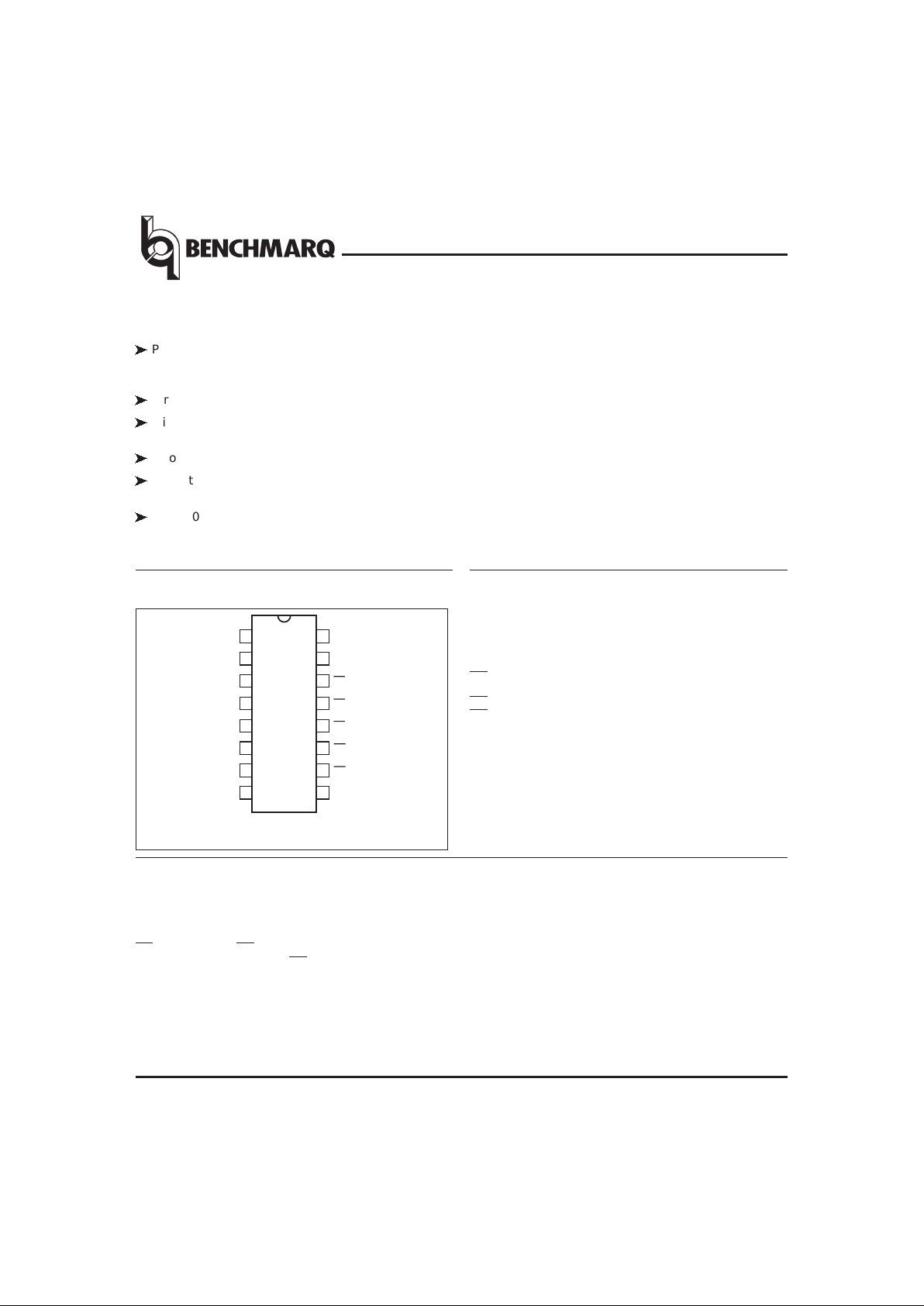
1
PN220401.eps
16-Pin Narrow DIP or SOIC
2
3
4
5
6
7
8
16
15
14
13
12
11
10
9
V
CC
BC
1
CE
CE
CON1
CE
CON2
CE
CON3
CE
CON4
NC
V
OUT
BC
2
NC
A
B
NC
THS
V
SS
Pin Names
V
OUT
Supply output
BC1–BC23 volt primary backup cell inputs
THS Threshold select input
CE chip-enable active low input
CE
CON1
– Conditioned chip-enable outputs
CE
CON4
A–B Decoder inputs
NC No connect
V
CC
+5 volt supply input
V
SS
Ground
Up to four banks of CMOS static RAM can be batterybacked using the V
OUT
and conditioned chip-enable output pins from the bq2204A. As VCCslews down during
a power failure, the conditioned chip-enable outputs
CE
CON1
through CE
CON4
are forced inactive independ-
ent of the chip-enable input CE
.
This activity unconditionally write-protects the external
SRAM as V
CC
falls below an out-of-tolerance threshold
V
PFD.VPFD
is selected by the threshold select input pin,
THS. If THS is tied to VSS, the power-fail detection occurs
at 4.62V typical for 5% supply operation.
If THS is tied to V
CC
, power-fail detection occurs at
4.37V typical for 10% supply operation. The THS pin
must be tied to VSSor VCCfor proper operation.
If a memory access is in process to any of the four external
banks of SRAM during power-fail detection, that memory
cycle continues to completion before the memory is writeprotected. If the memory cycle is not terminated within
time t
WPT
, all four chip-enable outputs are unconditionally
driven high,write-protectingthecontrolledSRAMs.
Pin Connections
Functional Description
As the supply continues to fall past V
PFD
, an internal
switching device forces V
OUT
to one of the two external
backup energy sources. CE
CON1
through CE
CON4
are
held high by the V
OUT
energy source.
During power-up, V
OUT
is switched back to the 5V supply as VCCrises above the backup cell input voltage
sourcing V
OUT
. Outputs CE
CON1
through CE
CON4
are
held inactive for time t
CER
(120ms maximum) after the
power supply has reached V
PFD
, independent of the CE
input,toallowforprocessorstabilization.
During power-valid operation, the CE
input is passed
through to one of the four CE
CON
outputs with a propagation delay of less than 10ns. The CE input is output
on one of the four CE
CON
output pins depending on the
level of the decode inputs at A and B as shown in the
Truth Table.
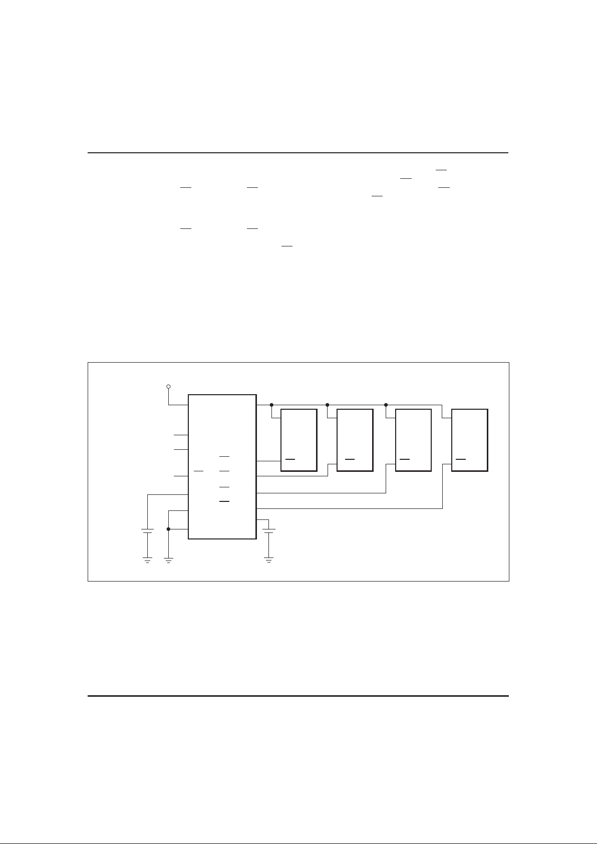
The A and B inputs are usually tied to high-order address pins so that a large nonvolatile memory can be designed using lower-density memory devices. Nonvolatility
and decoding are achieved by hardware hookup as shown
in Figure 1.
2
bq2204A
FG220401.eps
CE
BC
2
THS
V
SS
V
OUT
bq2204A
V
CC
CE
CMOS
SRAM
V
CC
5V
From Address
Decoder
CE
CON2
BC
1
CE
CON1
V
CC
CE
CMOS
SRAM
3V
Primary
Cell
3V
Primary
Cell
B
A
V
CC
CE
CMOS
SRAM
V
CC
CE
CMOS
SRAM
CE
CON3
CE
CON4
Figure 1. Hardware Hookup (5% Supply Operation)
Dec. 1992B
Energy Cell Inputs—BC1,BC
2
Two backup energy source inputs are provided on the
bq2204A. The BC1and BC2inputs accept a 3V primary
battery (non-rechargeable), typically some type of lithium chemistry. If no primary cell is to be used on either
BC1or BC2,theunusedinputshouldbetiedtoVSS.
V
CC
falling below V
PFD
starts the comparison of BC
1
and BC2. The BC input comparison continues until V
CC
rises above VSO. Power to V
OUT
begins with BC1and
switches to BC2only when V
BC1
is less than V
BC2
mi-
nus V
BSO
. The controller alternates to the higher BC
voltage only when the difference between the BC input
voltages is greater than V
BSO
. Alternating the backup
batteries allows one-at-a-time battery replacement and
efficient use of both backup batteries.
To prevent battery drain when there is no valid data to
retain, V
OUT
and CE
CON1-4
are internally isolated from
BC1and BC2by either of the following conditions:
■
Initial connection of a battery to BC1or BC2,or
■
Presentation of an isolation signal on CE.
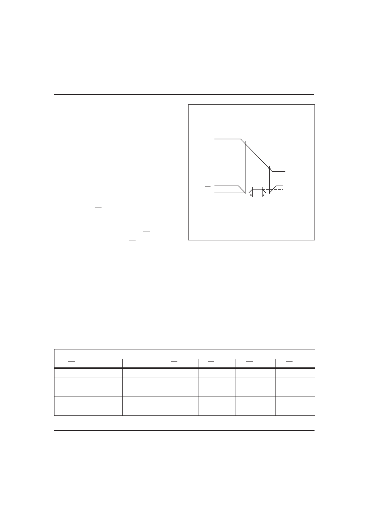
A valid isolation signal requires CE
low as VCCcrosses
both V
PFD
and VSOduring a power-down. See Figure 2.
Between these two points in time, CE must be brought
to the point of (0.48 to 0.52)*VCCand held for at least
700ns. The isolation signal is invalid if CE exceeds
0.54*VCCat any point between VCCcrossing V
PFD
and
VSO.
The appropriate battery is connected to V
OUT
and
CE
CON1–4
immediately on subsequent application and
removal of VCC.
3
TD220201.eps
V
CC
CE
V
PFD
V
SO
0.5 V
CC
700ns
Figure 2. Battery Isolation Signal
Dec. 1992 B
Truth Table
Input Output
CE ABCE
CON1
CE
CON2
CE
CON3
CE
CON4
HX X H H H H
LL L L H H H
LH L H L H H
LL H H H L H
LH H H H H L
bq2204A
4
bq2204A
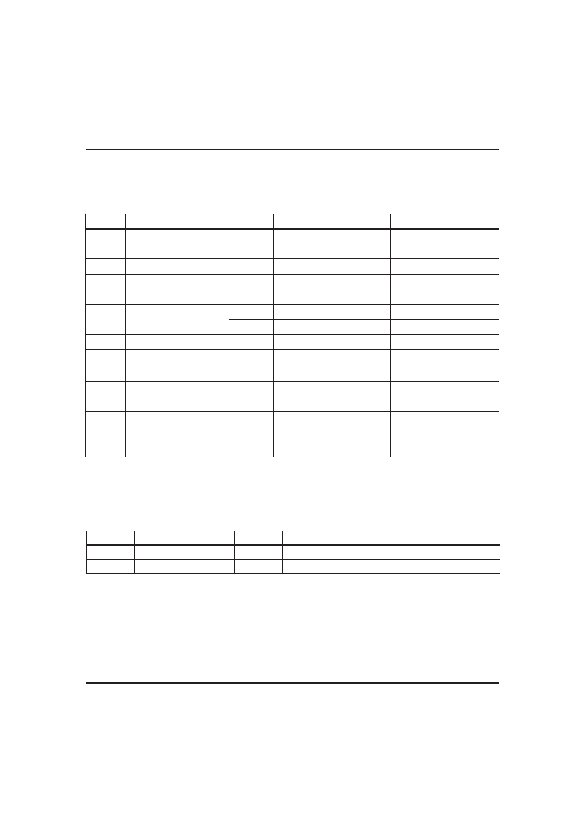
Recommended DC Operating Conditions (T
A=TOPR
)
Symbol Parameter Minimum Typical Maximum Unit Notes
V
CC
Supply voltage
4.75 5.0 5.5 V THS = V
SS
4.50 5.0 5.5 V THS = V
CC
V
SS
Supply voltage 0 0 0 V
V
IL
Input low voltage -0.3 - 0.8 V
V
IH
Input high voltage 2.2 - VCC+ 0.3 V
V
BC1
,
V
BC2
Backup cell voltage 2.0 - 4.0 V VCC<V
BC
THS Threshold select -0.3 - VCC+ 0.3 V
Note: Typical values indicate operation at TA= 25°C, VCC=5VorVBC.
Absolute Maximum Ratings
Symbol Parameter Value Unit Conditions
V
CC
DC voltage applied on VCCrelative to V
SS
-0.3 to +7.0 V
V
T
DC voltage applied on any pin excluding V
CC
relative to V
SS
-0.3 to +7.0 V V
T
≤
V
CC
+ 0.3
T
OPR
Operating temperature
0 to 70 °C Commercial
-40 to +85 °C Industrial “N”
T
STG
Storage temperature -55 to +125 °C
T
BIAS
Temperature under bias -40 to +85 °C
T
SOLDER
Soldering temperature 260 °C For 10 seconds
I
OUT
V
OUT
current 200 mA
Note: Permanent device damage may occur if Absolute Maximum Ratings are exceeded.Functional operation
should be limited to the Recommended DC Operating Conditions detailed in this data sheet. Exposure to conditions beyond the operational limits for extended periods of time may affect device reliability.
Dec. 1992 B
5
DC Electrical Characteristics (T
A=TOPR,VCC
=5V±10%)
Symbol Parameter Minimum Typical Maximum Unit Conditions/Notes
I
LI
Input leakage current - -
±
1
µ
AVIN=VSSto V
CC
V
OH
Output high voltage 2.4 - - V IOH= -2.0mA
V
OHB
VOH, BC supply VBC- 0.3 - - V
VBC>VCC,IOH= -10µA
V
OL
Output low voltage - - 0.4 V IOL= 4.0mA
I
CC
Operating supply current - 3 6 mA No load on outputs.
V
PFD
Power-faildetect voltage
4.55 4.62 4.75 V THS = V
SS
4.30 4.37 4.50 V THS = V
CC
V
SO
Supply switch-over voltage - V
BC
-V
I
CCDR
Data-retention mode
current
- - 100 nA
V
OUT
data-retention current
to additional memory not included.
V
BC
Active backup cell
voltage
-V
BC1
-VV
BC1>VBC2+VBSO
-V
BC2
-VV
BC2>VBC1+VBSO
V
BSO
Battery switch-over voltage 0.25 0.4 0.6 V
I
OUT1
V
OUT
current - - 160 mA V
OUT>VCC
- 0.3V
I
OUT2
V
OUT
current - 100 -
µA
V
OUT>VBC
- 0.2V
Note: Typical values indicate operation at TA= 25°C, VCC=5VorVBC.
Capacitance (T
A
= 25°C, F = 1MHz, VCC= 5.0V)
Symbol Parameter Minimum Typical Maximum Unit Conditions
C
IN
Input capacitance - - 8 pF Input voltage = 0V
C
OUT
Output capacitance - - 10 pF Output voltage = 0V
Note: This parameter is sampled and not 100% tested.
Dec. 1992 B
bq2204A

6
AC Test Conditions
Parameter Test Conditions
Input pulse levels 0V to 3.0V
Input rise and fall times 5ns
Input and output timing reference levels 1.5V (unless otherwise specified)
FG220102.eps
5V
960
100pF
CE
CON
510
Figure 3. Output Load
Power-Fail Control (T
A=TOPR
)
Symbol Parameter Minimum Typical Maximum Unit Notes
t
PF
VCCslew, 4.75V to 4.25V 300 - -
µ
s
t
FS
VCCslew, 4.25V to V
SO
10 - -
µ
s
t
PU
VCCslew, 4.25V to 4.75V 0 - -
µ
s
t
CED
chip-enable propagation delay - 7 10 ns
t
AS
A,B set up to CE 0--ns
t
CER
chip-enable recovery 40 80 120 ms
Time during which SRAM is
write-protected after V
CC
passes V
PFD
on power-up.
t
WPT
Write-protect time 40 100 150
µ
s
Delay after VCCslews down
past V
PFD
before SRAM is
write-protected.
Note: Typical values indicate operation at TA= 25°C, VCC=5V.
Caution: Negative undershoots below the absolute maximum rating of -0.3V in battery-backup mode
may affect data integrity.
Dec. 1992 B
bq2204A

7
TD220102.eps
V
CC
CE
CON
t
PF
t
FS
4.75
V
PFD
4.25
V
SO
t
WPT
V
OHB
CE
Power-Down Timing
TD220103.eps
V
CC
t
PU
CE
CE
CON
V
OHB
V
SO
4.25
V
PFD
4.75
t
CER
t
CED
t
CED
Power-Up Timing
Dec. 1992 B
TD220402.eps
CE
CON1
t
AS
CE
CE
CON4
A,B
t
CED
t
CED
Address-Decode Timing
bq2204A

8
bq2204A
16-Pin DIP Narrow (PN)
16-Pin PN(DIP Narrow
)
Dimension Minimum Maximum
A 0.160 0.180
A1 0.015 0.040
B 0.015 0.022
B1 0.055 0.065
C 0.008 0.013
D 0.740 0.770
E 0.300 0.325
E1 0.230 0.280
e 0.300 0.370
G 0.090 0.110
L 0.115 0.150
S 0.020 0.040
All dimensions are in inches.
Dec. 1992 B

9
bq2204A
16-Pin SOIC Narrow (SN)
A
A1
.004
C
B
e
D
E
H
L
16-Pin SN(SOIC Narrow
)
Dimension Minimum Maximum
A 0.060 0.070
A1 0.004 0.010
B 0.013 0.020
C 0.007 0.010
D 0.385 0.400
E 0.150 0.160
e 0.045 0.055
H 0.225 0.245
L 0.015 0.035
All dimensions are in inches.
Dec. 1992 B

10
bq2204A
Dec. 1992 B
Data Sheet Revision History
Change No. Page No. Description of Change Nature of Change
1 All bq2204A replaces bq2204.
1 1, 4–5 10% tolerance requires the THS
pin to be tied to V
CC
, not V
OUT
.
1 3 Energy cell input selection pro-
cess alternates between BC
1
and
BC2.
Note: Change 1 = Dec. 1992 changes from Sept. 1991

11
bq2204A
Ordering Information
bq2204A
PackageOption:
PN = 16-pin narrow plastic DIP
SN = 16-pin narrow SOIC
Device:
bq2204A Nonvolatile SRAM Controller
TemperatureRange:
blank = Commercial (0 to 70°C)
N = Industrial (-40 to +85°C)
Dec. 1992 B

IMPORTANT NOTICE
T exas Instruments and its subsidiaries (TI) reserve the right to make changes to their products or to discontinue
any product or service without notice, and advise customers to obtain the latest version of relevant information
to verify, before placing orders, that information being relied on is current and complete. All products are sold
subject to the terms and conditions of sale supplied at the time of order acknowledgement, including those
pertaining to warranty, patent infringement, and limitation of liability.
TI warrants performance of its semiconductor products to the specifications applicable at the time of sale in
accordance with TI’s standard warranty. Testing and other quality control techniques are utilized to the extent
TI deems necessary to support this warranty. Specific testing of all parameters of each device is not necessarily
performed, except those mandated by government requirements.
CERT AIN APPLICATIONS USING SEMICONDUCTOR PRODUCTS MAY INVOLVE POTENTIAL RISKS OF
DEATH, PERSONAL INJURY, OR SEVERE PROPERTY OR ENVIRONMENTAL DAMAGE (“CRITICAL
APPLICATIONS”). TI SEMICONDUCTOR PRODUCTS ARE NOT DESIGNED, AUTHORIZED, OR
WARRANTED TO BE SUITABLE FOR USE IN LIFE-SUPPORT DEVICES OR SYSTEMS OR OTHER
CRITICAL APPLICATIONS. INCLUSION OF TI PRODUCTS IN SUCH APPLICA TIONS IS UNDERSTOOD T O
BE FULLY AT THE CUSTOMER’S RISK.
In order to minimize risks associated with the customer’s applications, adequate design and operating
safeguards must be provided by the customer to minimize inherent or procedural hazards.
TI assumes no liability for applications assistance or customer product design. TI does not warrant or represent
that any license, either express or implied, is granted under any patent right, copyright, mask work right, or other
intellectual property right of TI covering or relating to any combination, machine, or process in which such
semiconductor products or services might be or are used. TI’s publication of information regarding any third
party’s products or services does not constitute TI’s approval, warranty or endorsement thereof.
Copyright 1999, Texas Instruments Incorporated
 Loading...