

Features
ä
Power monitoring and switching
for nonvolatile control of SRAMs
ä
Write-protect control
ä
Battery-low and battery-fail indicators
ä
Reset output for system power-on
reset
ä
Input decoder for control of up to
2 banks of SRAM
ä
3-volt primary cell input
ä
3-volt rechargeable battery input/output
General Description
The CMOS bq2203A SRAM Nonvolatile
Controller With Battery Monitor provides all the necessary functions for converting one or two banks of standard
CMOS SRAM into nonvolatile
read/write memory. The bq2203A is
compatible with the Personal Computer
Memory Card International Association
(PCMCIA) recommendations for
battery-backed static RAM memory
cards.
A precision comparator monitors the 5V
V
CC
input for an out-of-tolerance condition. When out of tolerance is detected,
the two conditioned chip-enable outputs
are forced inactive to write-protect
banks of SRAM.
Power for the external SRAMs is
switched from the VCCsupply to the
battery-backup supply as VCCdecays. On a subsequent power-up, the
V
OUT
supply is automatically
switched from the backup supply to
the VCCsupply. The external SRAMs
are write-protected until a powervalid condition exists. The reset output provides power-fail and power-on
resets for the system. The battery
monitor indicates battery-low and
battery-fail conditions.
During power-valid operation, the
input decoder selects one of two
banks of SRAM.
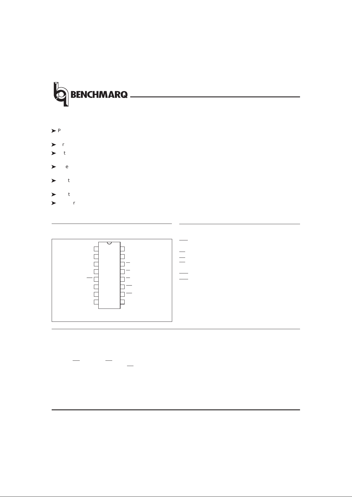
1
1
PN220301.eps
16-Pin Narrow DIP or SOIC
2
3
4
5
6
7
8
16
15
14
13
12
11
10
9
V
CC
BC
S
CE
CE
CON1
CE
CON2
BCL
RST
NC
V
OUT
BC
P
NC
A
BCF
NC
THS
V
SS
bq2203A
Nov.1994 B
Pin Connections
Two banks of CMOS static RAM can be battery-backed using the V
OUT
and the conditioned chip-enable output pins
from the bq2203A. As the voltage input VCCslews down
during a power failure, the two conditioned chip-enable
outputs, CE
CON1
and CE
CON2
, are forced inactive
independent of the chip-enable input CE.
This activity unconditionally write-protects external SRAM
as V
CC
falls to an out-of-tolerance threshold V
PFD.VPFD
is
selected by the threshold select input pin, THS. If THS is
tied to VSS, the power-fail detection occurs at 4.62V typical
for 5% supply operation.
If THS is tied to VCC, power-fail detection occurs at
4.37V typical for 10% supply operation. The THS pin
must be tied to VSSor VCCfor proper operation.
If a memory access is in process to any of the two external banks of SRAM during power-fail detection, that
memory cycle continues to completion before the memory
is write-protected. If the memory cycle is not terminated
within time t
WPT
(150µs maximum), the two chip-enable
outputs are unconditionally driven high, write-protecting
the controlled SRAMs.
Functional Description
NV Controller With Battery Monitor
Pin Names
V
OUT
Supply output
RST Reset output
THS Threshold select input
CE chip-enable active low input
CE
CON1
, Conditioned chip-enable outputs
CE
CON2
A Bank select input
BCF Battery fail push-pull output
BCL Battery low push-pull output
BC
P
3V backup supply input
BC
S
3V rechargeable backup supply input/output
NC No connect
V
CC
5-volt supply input
V
SS
Ground
As the supply continues to fall past V
PFD
, an internal
switching device forces V
OUT
to the external backup en-
ergy source. CE
CON1
and CE
CON2
are held high by the
V
OUT
energy source.
During power-up, V
OUT
is switched back to the 5V supply as VCCrises above the backup cell input voltage
sourcing V
OUT
. Outputs CE
CON1
and CE
CON2
are held
inactive for time t
CER
(120ms maximum) after the
power supply has reached V
PFD
, independent of the CE
input,toallowforprocessorstabilization.
During power-valid operation, the CE
input is passed
through to one of the two CE
CON
outputs with a propagation delay of less than 10ns. The CE input is output on
one of the two CE
CON
output pins depending on the level
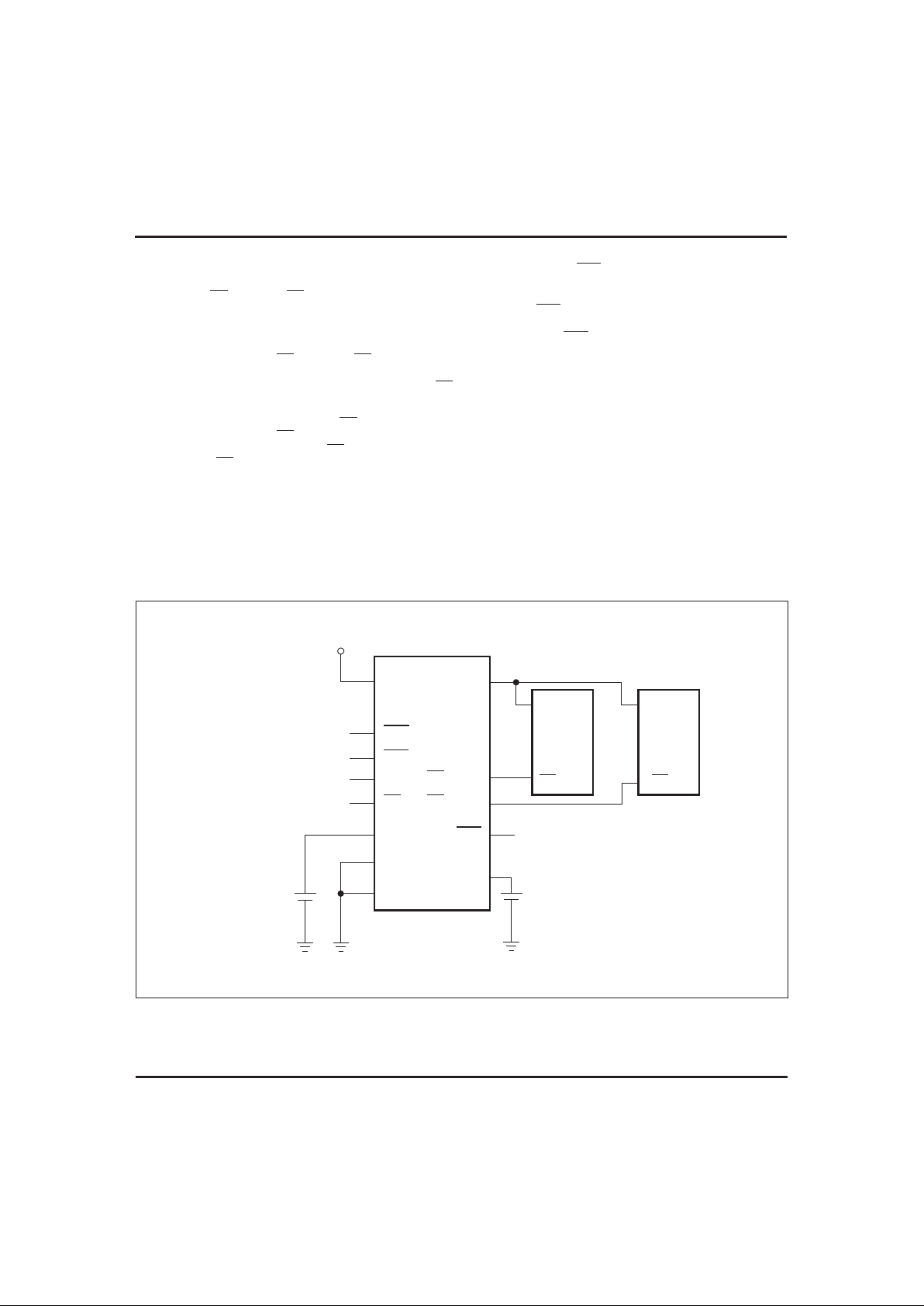
of bank select input A,asshownintheTruthT able .
Bank select input A is usually tied to a high-order ad-
dress pin so that a large nonvolatile memory can be designed using lower-density memory devices. Nonvolatility and decoding are achieved by hardware hookup as
shown in Figure 1.
The reset output (RST) goes active within t
PFD
(150µs
maximum) after V
PFD,
and remains active for a minimum of 40ms (120ms maximum) after power returns
valid. The RST output can be used as the power-on reset for a microprocessor. Access to the external RAM
may begin when RST returns inactive.
Energy Cell Inputs—BCP,BC
S
Two backup energy source inputs are provided on the
bq2203A—a primary cell BC
P
and a secondary cell BCS.
The primary cell input is designed to accept any 3V primary battery (non-rechargeable), typically some type of
lithium chemistry.If a primary cell is not to be used, the
BCPpin should be tied to VSS. The secondary cell input
BCSis designed to accept constant-voltage currentlimited rechargeable cells.
During normal 5V power valid operation, 3.3V typical is output on the BC
S
pin and is current-limited internally . Although this charging method can be used with various 3V
secondary cells, it is specifically designed for a Panasonic VL
(vanadium-lithium) series of rechargeable cells.
2
FG220301.eps
CE
BC
P
THS
V
SS
V
OUT
bq2203A
V
CC
CE
CMOS
SRAM
V
CC
5V
From Address
Decoder
CE
CON2
BC
S
CE
CON1
A
RST
V
CC
CE
CMOS
SRAM
To Microprocessor
3V Secondary
Cell
3V Primary
Cell
BCL
BCF
Figure 1. Hardware Hookup (5% Supply Operation)
Nov.1994 B
bq2203A
If a secondary cell is not to be used, the BCSpin must be
tied directly to VSS.
V
CC
falling below V
PFD
starts the comparison of BC
S
and BCP. The BC input comparison continues until V
CC
rises above VSO. Power to V
OUT
begins with BCSand
switches to BCPonly when BCSis less than BCPminus
V
BSO
. The controller alternates to the higher BC voltage
when the difference between the BC input voltages is
greater than V
BSO
. Alternating the backup batteries allows one-at-a-time battery replacement and efficient use
of both backup batteries.
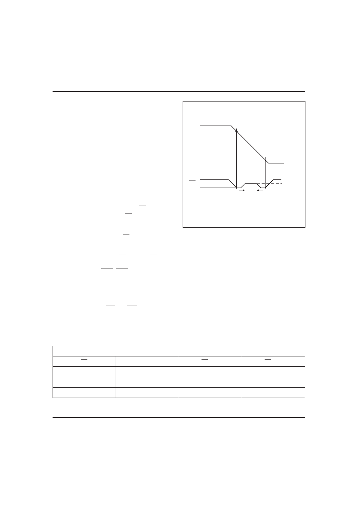
To prevent battery drain when there is no valid data to
retain, V
OUT
,CE
CON1
, and CE
CON2
are internally iso-
lated from BCPand BCSby either of two methods:
■
Initial connection of a battery to BCPor BCS(V
CC
grounded) or
■
Presentation of an isolation signal on CE.
A valid isolation signal requires CE
low as VCCcrosses
both V
PFD
and VSOduring a power-down. See Figure
2. Between these two points in time, CE must be
brought to V
CC
*
(0.48 to 0.52) and held for at least 700ns.
The isolation signal is invalid if CE exceeds V
CC
*
0.54 at
any point between VCCcrossing V
PFD
and VSO.
The isolation function is terminated and the appropriate
battery is connected to V
OUT
,CE
CON1
, and CE
CON2
by
powering VCCup through V
PFD
.
Battery Monitor—BCL, BCF
As VCCrises past V
PFD
, the battery voltage on BCPis
compared with a dual-voltage reference. The result of
this comparison is latched internally, and output after
tBCwhen VCCrises past V
PFD
. If the battery voltage on
BCPis below VBL, then BCL is asserted low. If the battery is below VBF, then BCL and BCF are asserted low.
The results of this comparison remain latched until V
CC
falls below V
PFD
.
3
TD220101.eps
V
CC
CE
V
PFD
V
SO
0.5 V
CC
700ns
Figure 2. Battery Isolation Signal
Truth Table
Input Output
CE
ACE
CON1
CE
CON2
HXHH
LLLH
LHHL
Nov.1994 B
bq2203A
4
Recommended DC Operating Conditions (T
A=TOPR
)
Symbol Parameter Minimum Typical Maximum Unit Notes
V
CC
Supply voltage
4.75 5.0 5.5 V THS = V
SS
4.50 5.0 5.5 V THS = V
CC
V
BCP
Backup cell input voltage
2.0 - 4.0 V VCC<V
BC
V
BCS
2.0 - 4.0 V VCC<V
BC
V
SS
Supply voltage 0 0 0 V
V
IL
Input low voltage -0.3 - 0.8 V
V
IH
Input high voltage 2.2 - VCC+ 0.3 V
THS Threshold select -0.3 - VCC+ 0.3 V
Note: Typical values indicate operation at TA= 25°C, VCC=5V.
Absolute Maximum Ratings
Symbol Parameter Value Unit Conditions
V
CC
DC voltage applied on VCCrelative to V
SS
-0.3 to +7.0 V
V
T
DC voltage applied on any pin excluding V
CC
relative to V
SS
-0.3 to +7.0 V V
T
≤
V
CC
+ 0.3
T
OPR
Operating temperature
0 to 70 °C Commercial
-40 to +85 °C “N” Industrial
T
STG
Storage temperature -55 to +125 °C
T
BIAS
Temperature under bias -40 to +85 °C
T
SOLDER
Soldering temperature 260 °C For 10 seconds
I
OUT
V
OUT
current 200 mA
Note: Permanent device damage may occur if Absolute Maximum Ratings are exceeded. Functional opera-
tion should be limited to the Recommended DC Operating Conditions detailed in this data sheet. Exposure to conditions beyond the operational limits for extended periods of time may affect device reliability.
Nov.1994 B
bq2203A

5
DC Electrical Characteristics (T
A=TOPR,VCC
=5V±10%)
Symbol Parameter Minimum Typical Maximum Unit Conditions/Notes
I
LI
Input leakage current - -
±
1
µ
AVIN=VSSto V
CC
V
OH
Output high voltage 2.4 - - V IOH= -2.0mA
V
OHB
VOH, backup supply VBC- 0.3 - - V
VBC>VCC,IOH= -10µA
V
OL
Output low voltage - - 0.4 V IOL= 4.0mA
I
CC
Operating supply current - 3 6 mA No load on outputs
V
PFD
Power-faildetect voltage
4.55 4.62 4.75 V THS = V
SS
4.30 4.37 4.50 V THS = V
CC
V
SO
Supply switch-over voltage - V
BC
-V
I
CCDR
Data-retention mode
current
- - 100 nA No load on outputs
V
BC
Active backup cell voltage
-V
BCS
-VV
BCS>VBCP+VBSO
-V
BCP
-VV
BCP>VBCS+VBSO
V
BSO
Battery switch-over voltage 0.25 0.4 0.6 V
R
BCS
BC
S
charge output internal
resistance
500 1000 1750
Ω
V
BCSO
≥
3.0V
V
BCSO
BCScharge output voltage 3.15 3.3 3.5 V
V
CC>VPFD
, RST inactive,
full charge or no load
I
OUT1
V
OUT
current - - 160 mA V
OUT
≥
V
CC
- 0.3V
I
OUT2
V
OUT
current - 100 -
µ
AV
OUT
≥
V
BC
- 0.2V
V
BL
Voltagebattery low 2.3 - 2.5 V BCPinput only
V
BF
Voltagebattery fail 2.0 - 2.2 V BCPinput only
Note: Typical values indicate operation at TA= 25°C, VCC=5VorVBC.
Capacitance (T
A
= 25°C, F = 1MHz, VCC= 5.0V)
Symbol Parameter Minimum Typical Maximum Unit Conditions
C
IN
Input capacitance - - 8 pF Input voltage = 0V
C
OUT
Output capacitance - - 10 pF Output voltage = 0V
Note: This parameter is sampled and not 100% tested.
Nov.1994 B
bq2203A
bq2203A

6
AC Test Conditions
Parameter Test Conditions
Input pulse levels 0V to 3.0V
Input rise and fall times 5ns
Input and output timing reference levels 1.5V (unless otherwise specified)
Output load (including scope and jig) See Figure 3
FG220102.eps
5V
960
100pF
CE
CON
510
Figure 3. Output Load
Nov.1994 B
Power-Fail Control (TA=T
OPR
)
Symbol Parameter Min. Typ. Max. Unit Conditions
t
PF
VCCslew 4.75 to 4.25 V 300 - -
µ
s
t
FS
VCCslew 4.25 V to V
SO
10 - -
µ
s
t
PU
VCCslew 4.25 to 4.75 V 0 - -
µ
s
t
CED
Chip-enable propagation delay 7 10 ns
t
CER
Chip-enable recovery time 40 80 120 ms
Time during which SRAM is writeprotected after VCCpasses V
PFD
on
power-up
t
RR
V
PFD
to RST inactive t
CER
-t
CER
ms
Time, after V
CC
becomes valid, before
RST is cleared
t
AS
Input A set up to CE 0--ns
t
WPT
Write-protect time 40 100 150µs
Delay after V
CC
slews down past
V
PFD
before SRAM is write-protected
t
R
V
PFD
to RST active t
WPT
-t
WPT
µ
s
Delay after V
CC
slews down past
V
PFD
before RST is active
t
BC
V
PFD
to BCL/BCF active t
CER
-t
CER
ms
Delay after V
CC
slews up past V
PFD
before BCL or BCF is active
Note: Typical values indicate operation at TA= 25°C, VCC=5V.
Caution: Negative undershoots below the absolute maximum rating of -0.3V in battery-backup mode
may affect data integrity.
bq2203A

7
TD220202.eps
V
CC
CE
CON
t
PF
t
FS
4.75
V
PFD
4.25
V
SO
t
WPT
V
OHB
CE
t
R
RST
Power-Down Timing
TD220302.eps
V
CC
t
PU
CE
CE
CON
V
OHB
V
SO
4.25
V
PFD
4.75
t
CER
t
CED
t
CED
RST
BCL
BCF
t
RR
t
BC
Power-Up Timing
Nov.1994 B
bq2203A
TD220204.eps
CE
CON1
t
AS
CE
CE
CON2
A
t
CED
t
CED
Address-Decode Timing

8
bq2203A
Nov.1994 B
16-Pin SOIC Narrow
A
A1
.004
C
B
e
D
E
H
L
16-Pin SN(SOIC Narrow
)
Dimension Minimum Maximum
A 0.060 0.070
A1 0.004 0.010
B 0.013 0.020
C 0.007 0.010
D 0.385 0.400
E 0.150 0.160
e 0.045 0.055
H 0.225 0.245
L 0.015 0.035
All dimensions are in inches.

9
bq2203A
Nov.1994 B
16-Pin DIPNarrow
16-Pin PN(DIP Narrow
)
Dimension Minimum Maximum
A 0.160 0.180
A1 0.015 0.040
B 0.015 0.022
B1 0.055 0.065
C 0.008 0.013
D 0.740 0.770
E 0.300 0.325
E1 0.230 0.280
e 0.300 0.370
G 0.090 0.110
L 0.115 0.150
S 0.020 0.040
All dimensions are in inches.

10
bq2203A
Nov.1994 B
Data Sheet Revision History
Change No. Page No. Description Nature of Change
1 - Changed data sheet from “Preliminary”to “Final”
15
Changed maximum charge output internal resistance (R
BCS
)
Was:1500Ω
Is: 1750Ω
Note: Change 1 = Nov.1994 B changes from Dec. 1992 A.

11
bq2203A
Nov.1994 B
bq2203A
PackageOption:
PN = 16-pin plastic DIP Narrow
SN = 16-pin SOIC Narrow
Device:
bq2203A SRAM Nonvolatile Controller
WithBatteryMonitorandReset
*Contact factory for availability.
Ordering Information
TemperatureRange:
blank = Commercial (0 to +70°C)
N = Industrial (-40 to +85°C)*

IMPORTANT NOTICE
T exas Instruments and its subsidiaries (TI) reserve the right to make changes to their products or to discontinue
any product or service without notice, and advise customers to obtain the latest version of relevant information
to verify, before placing orders, that information being relied on is current and complete. All products are sold
subject to the terms and conditions of sale supplied at the time of order acknowledgement, including those
pertaining to warranty, patent infringement, and limitation of liability.
TI warrants performance of its semiconductor products to the specifications applicable at the time of sale in
accordance with TI’s standard warranty. Testing and other quality control techniques are utilized to the extent
TI deems necessary to support this warranty. Specific testing of all parameters of each device is not necessarily
performed, except those mandated by government requirements.
CERT AIN APPLICATIONS USING SEMICONDUCTOR PRODUCTS MAY INVOLVE POTENTIAL RISKS OF
DEATH, PERSONAL INJURY, OR SEVERE PROPERTY OR ENVIRONMENTAL DAMAGE (“CRITICAL
APPLICATIONS”). TI SEMICONDUCTOR PRODUCTS ARE NOT DESIGNED, AUTHORIZED, OR
WARRANTED TO BE SUITABLE FOR USE IN LIFE-SUPPORT DEVICES OR SYSTEMS OR OTHER
CRITICAL APPLICATIONS. INCLUSION OF TI PRODUCTS IN SUCH APPLICA TIONS IS UNDERSTOOD T O
BE FULLY AT THE CUSTOMER’S RISK.
In order to minimize risks associated with the customer’s applications, adequate design and operating
safeguards must be provided by the customer to minimize inherent or procedural hazards.
TI assumes no liability for applications assistance or customer product design. TI does not warrant or represent
that any license, either express or implied, is granted under any patent right, copyright, mask work right, or other
intellectual property right of TI covering or relating to any combination, machine, or process in which such
semiconductor products or services might be or are used. TI’s publication of information regarding any third
party’s products or services does not constitute TI’s approval, warranty or endorsement thereof.
Copyright 1999, Texas Instruments Incorporated
 Loading...