

54ACT16646, 74ACT16646
16-BIT BUS TRANSCEIVERS AND REGISTERS
WITH 3-STATE OUTPUTS
SCAS127B – MARCH 1990 – REVISED APRIL 1996
D
Members of the Texas Instruments
Widebus
D
Inputs Are TTL-Voltage Compatible
D
Independent Registers for A and B Buses
D
Multiplexed Real-Time and Stored Data
D
Flow-Through Architecture Optimizes
t
Family
PCB Layout
D
Distributed VCC and GND Pin Configuration
Minimizes High-Speed Switching Noise
D
EPIC
t
(Enhanced-Performance Implanted
CMOS) 1-mm Process
D
500-mA Typical Latch-Up Immunity at
125°C
D
Package Options Include Plastic 300-mil
Shrink Small-Outline (DL) Packages Using
25-mil Center-to-Center Pin Spacings and
380-mil Fine-Pitch Ceramic Flat (WD)
Packages Using 25-mil Center-to-Center
Pin Spacings
description
The ’ACT16646 are 16-bit bus transceivers
consisting of D-type flip-flops and control circuitry
with 3-state outputs arranged for multiplexed
transmission of data directly from the data bus or
from the internal storage registers. The devices
can be used as two 8-bit transceivers or one 16-bit
transceiver. Data on the A or B bus is clocked into
the registers on the low-to-high transition of the
appropriate clock (CLKAB or CLKBA) input.
Figure 1 illustrates the four fundamental busmanagement functions that can be performed
with the bus transceivers and registers.
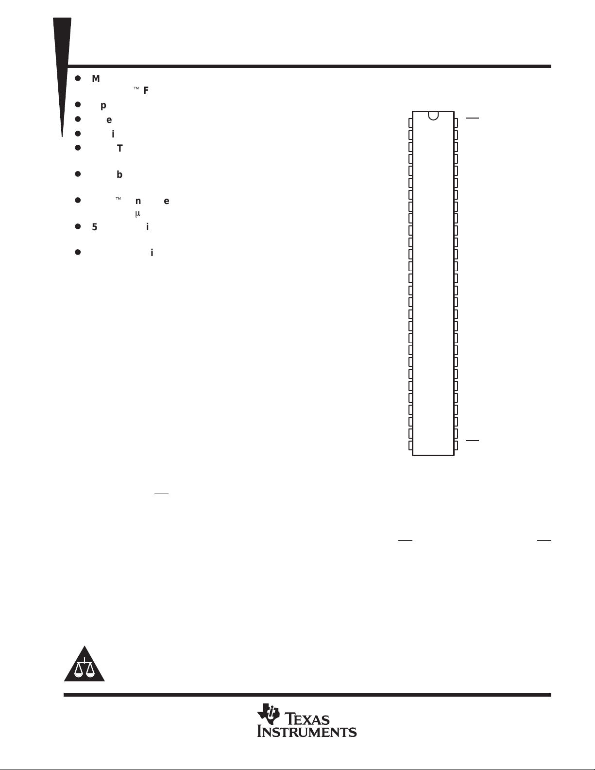
54ACT16646 . . . WD PACKAGE
74ACT16646 . . . DL PACKAGE
1CLKAB
1SAB
2SAB
2CLKAB
1DIR
GND
1A1
1A2
V
CC
1A3
1A4
1A5
GND
1A6
1A7
1A8
2A1
2A2
2A3
GND
2A4
2A5
2A6
V
CC
2A7
2A8
GND
2DIR
(TOP VIEW)
1
56
2
55
3
54
4
53
5
52
6
51
7
50
8
49
9
48
10
47
11
46
12
45
13
44
14
43
15
42
16
41
17
40
18
39
19
38
20
37
21
36
22
35
23
34
24
33
25
32
26
31
27
30
28
29
1OE
1CLKBA
1SBA
GND
1B1
1B2
V
CC
1B3
1B4
1B5
GND
1B6
1B7
1B8
2B1
2B2
2B3
GND
2B4
2B5
2B6
V
CC
2B7
2B8
GND
2SBA
2CLKBA
2OE
Output-enable (OE
) and direction-control (DIR) inputs are provided to control the transceiver functions. In the
transceiver mode, data present at the high-impedance port may be stored in either register or in both. The select
controls (SAB and SBA) can multiplex stored and real-time (transparent mode) data. The circuitry used for
select control eliminates the typical decoding glitch that occurs in a multiplexer during the transition between
stored and real-time data. DIR determines which bus receives data when OE is low. In the isolation mode (OE
high), A data may be stored in one register and/or B data may be stored in the other register.
When an output function is disabled, the input function is still enabled and may be used to store and transmit
data. Only one of the two buses, A or B, may be driven at a time.
The 74ACT16646 is packaged in TI’s shrink small-outline package, which provides twice the functionality of
standard small-outline packages in the same printed-circuit-board area.
The 54ACT16646 is characterized for operation over the full military temperature range of –55°C to 125°C. The
74ACT16646 is characterized for operation from –40°C to 85°C.
Please be aware that an important notice concerning availability, standard warranty, and use in critical applications of
Texas Instruments semiconductor products and disclaimers thereto appears at the end of this data sheet.
EPIC and Widebus are trademarks of Texas Instruments Incorporated.
UNLESS OTHERWISE NOTED this document contains PRODUCTION
DATA information current as of publication date. Products conform to
specifications per the terms of Texas Instruments standard warranty.
Production processing does not necessarily include testing of all
parameters.
POST OFFICE BOX 655303 • DALLAS, TEXAS 75265
Copyright 1996, Texas Instruments Incorporated
1

54ACT16646, 74ACT16646
16-BIT BUS TRANSCEIVERS AND REGISTERS
WITH 3-STATE OUTPUTS
SCAS127B – MARCH 1990 – REVISED APRIL 1996
BUS A
DIRLCLKABXCLKBAXSABXSBA
OE
L
REAL-TIME TRANSFER
BUS B TO BUS A
BUS B
L
OE
L
BUS A
DIRHCLKABXCLKBAXSABLSBA
REAL-TIME TRANSFER
BUS A TO BUS B
BUS B
X
BUS A
DIRXCLKAB CLKBAXSABXSBA
X
X
H
X
X
↑
XX
STORAGE FROM
A, B, OR A AND B
↑
↑↑
BUS B
OEOE
X
X
X
X
BUS A
DIRLCLKABXCLKBA
L
L H H or L X H X
TRANSFER STORED DA TA
Figure 1. Bus-Management Functions
H or L
TO A AND/OR B
BUS B
SABXSBA
H
2
POST OFFICE BOX 655303 • DALLAS, TEXAS 75265

OPERATION OR FUNCTION
54ACT16646, 74ACT16646
16-BIT BUS TRANSCEIVERS AND REGISTERS
WITH 3-STATE OUTPUTS
SCAS127B – MARCH 1990 – REVISED APRIL 1996
FUNCTION TABLE
INPUTS
OE DIR CLKAB CLKBA SAB SBA A1–A8 B1–B8
X X ↑ X X X Input Unspecified Store A, B unspecified
X XX ↑ X X Unspecified Input Store B, A unspecified
H X ↑ ↑ X X Input Input Store A and B data
H X H or L H or L X X Input Input Isolation, hold storage
L L X X X L Output Input Real-time B data to A bus
L L X H or L X H Output Input Stored B data to A bus
L H X X L X Input Output Real-time A data to B Bus
L H H or L X H X Input Output Stored A data to bus
†
The data-output functions may be enabled or disabled by various signals at OE or DIR. Data-input functions are always enabled, i.e., data at
the bus terminals is stored on every low-to-high transition of the clock inputs.
DATA I/O
†
{
{
POST OFFICE BOX 655303 • DALLAS, TEXAS 75265
3
 Loading...