

Telefunken TSOP7000 Datasheet
Vishay Telefunken
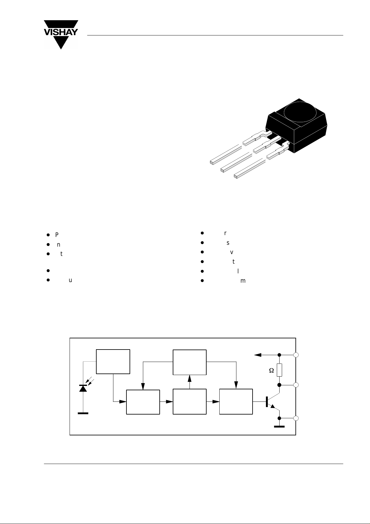
IR Receiver for High Data Rate PCM at 455kHz
Description
The TSOP7000 is a miniaturized receiver for infrared
remote control and IR data transmission. PIN diode
and preamplifier are assembled on lead frame, the
epoxy package is designed as IR filter.
The demodulated output signal can directly be
decoded by a microprocessor. The main benefit is the
operation with high data rates and long distances.
TSOP7000
14 500
Features
D
Photo detector and preamplifier in one package
D
Internal Bandfilter for PCM frequency
D
Internal shielding against electrical field
disturbance
D
TTL and CMOS compatibility
D
Output active low
Block Diagram
Input
PIN
AGC
Special Features
D
Data rate 20 kbit/s
D
Small size package
D
Supply voltage 2.7 – 5.5V
D
Short settling time after power on
D
High envelope duty cycle can be received
D
Enhanced immunity against disturbance
from energy saving lamps
Control
Circuit
Band
Pass
Demodu-
lator
10 k
3
V
S
W
1
OUT
2
GND
16499
Document Number 82147
www.vishay.com
1 (7)Rev. 3, 13-Mar-01

TSOP7000
Supply Current (Pin 3)
Transmission Distance
Rise time
Vishay Telefunken
Absolute Maximum Ratings
T
= 25_C
amb
Parameter Test Conditions Symbol Value Unit
Supply Voltage Pin 3 V
Voltage at output to supply Pin 1 VS – V
Supply Current Pin 3 I
Output Voltage Pin 1 V
Output Current Pin 1 I
S
O
S
O
O
Junction Temperature C 100
Storage Temperature Range T
Operating Temperature Range T
Soldering Temperature t x 10 s, 1 mm from case T
Power Consumption P
stg
amb
sd
tot
Basic Characteristics
T
= 25_C, VS = 5.0V
amb
Parameter Test Conditions Symbol Min Typ Max Unit
pp
Dark ambient I
Ev = 40 klx, sunlight I
Supply Voltage (Pin 3) V
lp= 870nm, IR Diode TSHF5400,
IF = 300 mA
lp= 950nm, IR Diode TSAL6400,
IF = 300 mA
Threshold Irradiance
lp = 870nm,
optical test signal of Fig.1
Maximum Irradiance Optical test signal of Fig.1 E
Output Voltage Low (Pin 1) 1kW external pull up resistor V
Output Voltage High (Pin 1) No external pull–up resistor V
Bandpassfilter quality Q 10
Out–Pulse width tolerance
Delay time of output pulse
Optical test signal of Fig.1,
1.5mW/m
2
≤ Ee ≤ 30W/m
2
Optical test signal of Fig.1,
E
> 1.5mW/m
e
2
Receiver start up time Valid data after power on t
Falling time Leading edge of output pulse t
No external pull up resistor t
1kW external pull up resistor t
Directivity Angle of half transmission distance ϕ
d
d
E
e min
e max
D
t
don
SD
SH
S
max
max
QL
QH
tpo
V
f
r
r
1/2
VS –
0.25
–15 +5 +15
–0.3...6.0 V
–0.3...VS+0.3 V
–0.3...6.0 V
15 mA
–25...+85
–25...+85
260
30 mW
2.0 2.7 mA
2.3 mA
2.7 5 5.5 V
20 m
12 m
0.8 1.5 mW/m
30 W/m
15 36
50
0.4
12
1.2
±45 deg
5 mA
°
C
°
C
°
C
°
C
100 mV
V
m
m
m
m
m
m
2
2
s
s
s
s
s
s
www.vishay.com
2 (7)
Document Number 82147
Rev. 3, 13-Mar-01
Optical Test Signal (f=455kHz, 10cycles/burst)
E
e
tpi = 22 µs
2.2 µs
TSOP7000
Vishay Telefunken
V
Q
V
QH
50%
V
QL
Application Circuit
TSHF5400
λp = 870nm
t
don
t
= t
15 µs
po
pi
TSOP7000
> 48.6 µs
(min. duty cycle)
Output Signal of TSOP7000
t
po
90%
10%
t
f
Figure 1. Output Function
3
1
2
C1 >100nF
recommended
t
r
R1 >1 kW
optional
t
16792
t
+5V *)
m
C
GND
*) tolerated supply voltage range: 2.7V < VS < 5.5V,
16498
With the resistor R1 the slopes of the output pulse are becoming faster.
Recommendation for Suitable Data Formats
The circuit of the TSOP7000 is designed in that way that disturbance signals are identified and unwated output
pulses due to noise or disturbances are avoided. A bandpassfilter , an automatic gain control and an integrator
stage is used to suppress such disturbances. The distinguishing marks between data signal and disturbance
are carrier frequency, burst length and the envelope duty cycle.
The data signal should fullfill the following conditions:
D
The carrier frequency should be close to 455kHz.
D
The burstlength should be at least 22ms (10 cycles of the carrier signal) and shorter than 500ms.
D
The separation time between two consecutive bursts should be at least 26ms.
D
If the data bursts are longer than 500ms then the envelope duty cycle is limited to 25%.
D
The duty cycle of the carrier signal (455kHz) may be between 50% (1.1ms pulses) and 10% (0.2.µs pulses).
The longer duty cycle may help to save battery power.
Document Number 82147
www.vishay.com
3 (7)Rev. 3, 13-Mar-01
 Loading...