Telefunken TSDF54040 Datasheet

TSDF54040
Vishay Telefunken
Dual - MOSMIC– two AGC Amplifiers for TV–Tuner
Prestage with 5 V Supply Voltage
MOSMIC - MOS Monolithic Integrated Circuit Electrostatic sensitive device.
Observe precautions for handling.
Applications
Low noise gain controlled input stages in UHF-and
VHF- tuner with 5 V supply voltage.
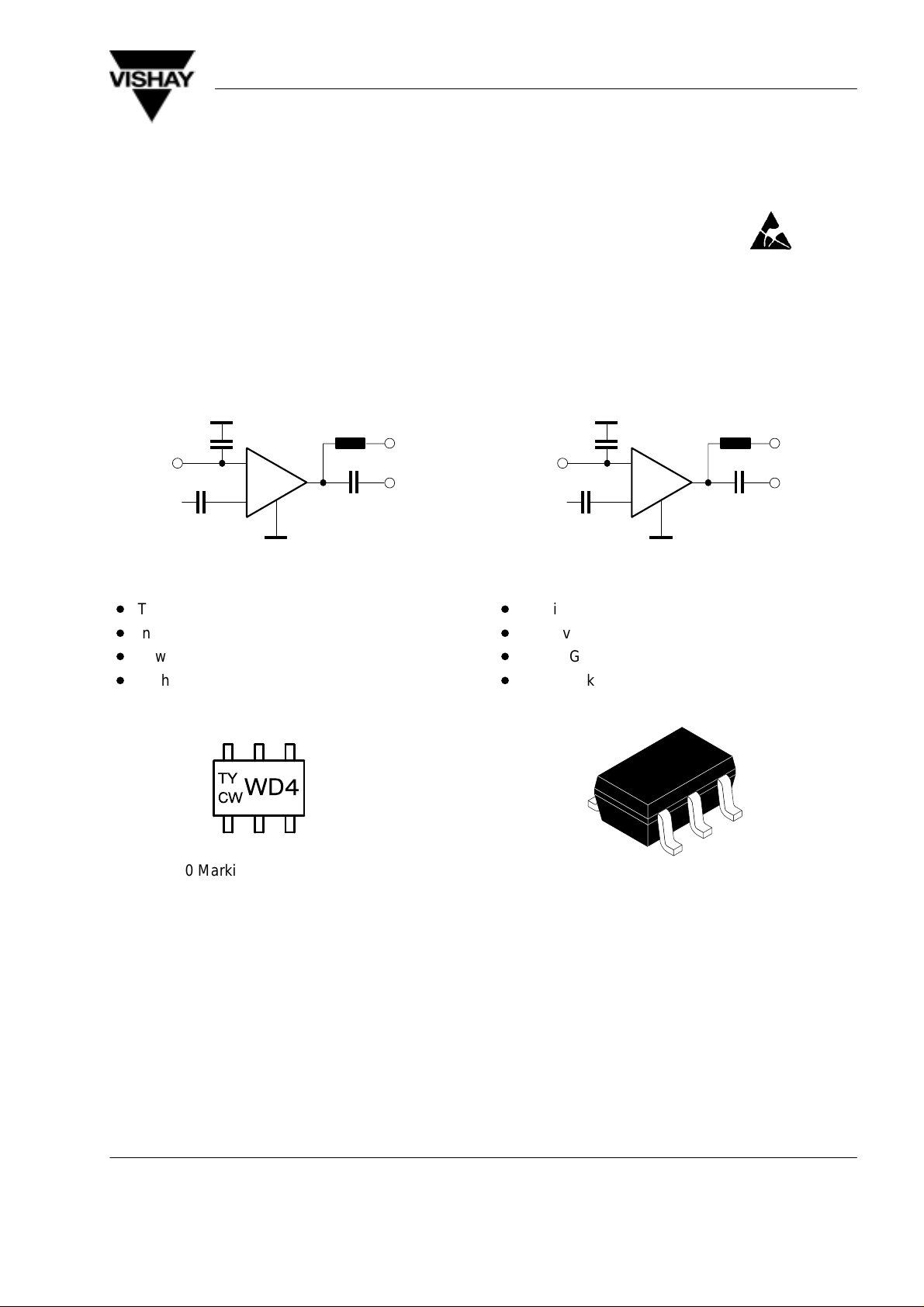
Typical Application
Amplifier 1
AGC
RF in
C block
C block
G2
G1
RFC
D
S
C block
V
DD
RF out
94 9296
Amplifier 2
AGC
RF in
C block
C block
G2
G1
RFC
D
S
C block
V
DD
RF out
94 9296
Features
D
D
Two AGC amplifiers in a single package
D
Integrated gate protection diodes
D
Low noise figure
D
High gain, high forward transadmittance
(40 mS typ.)
645
TY
WD4
CW
132
16022
TSDF54040 Marking: WD4
Plastic case (SOT 363)
1 = Gate 1 (amplifier 1), 2 = Gate 2, 3 = Drain (amplifier 1),
4 = Drain (amplifier 2), 5 = Source, 6 = Gate1 (amplifier 2)
T = Telefunken
Y = Year, is variable for digit from 0 to 9 (e.g. 9 = 1999, 0 = 2000)
CW = Calendar Week, is variable for number from 01 to 52
Number of Calendar Week is always indicating place of pin 1
Biasing network on chip
D
Improved cross modulation at gain reduction
D
High AGC-range
D
SMD package
16 015–2
Document Number 85071
Rev. 3, 16-Mar-99
www.vishay.de • FaxBack +1-408-970-5600
1 (5)

TSDF54040
Vishay Telefunken
All of following data and characteristics are valid for operating either
amplifier 1 (pin 1, 3, 2, 5) or amplifier 2 (pin 6, 4, 2, 5)
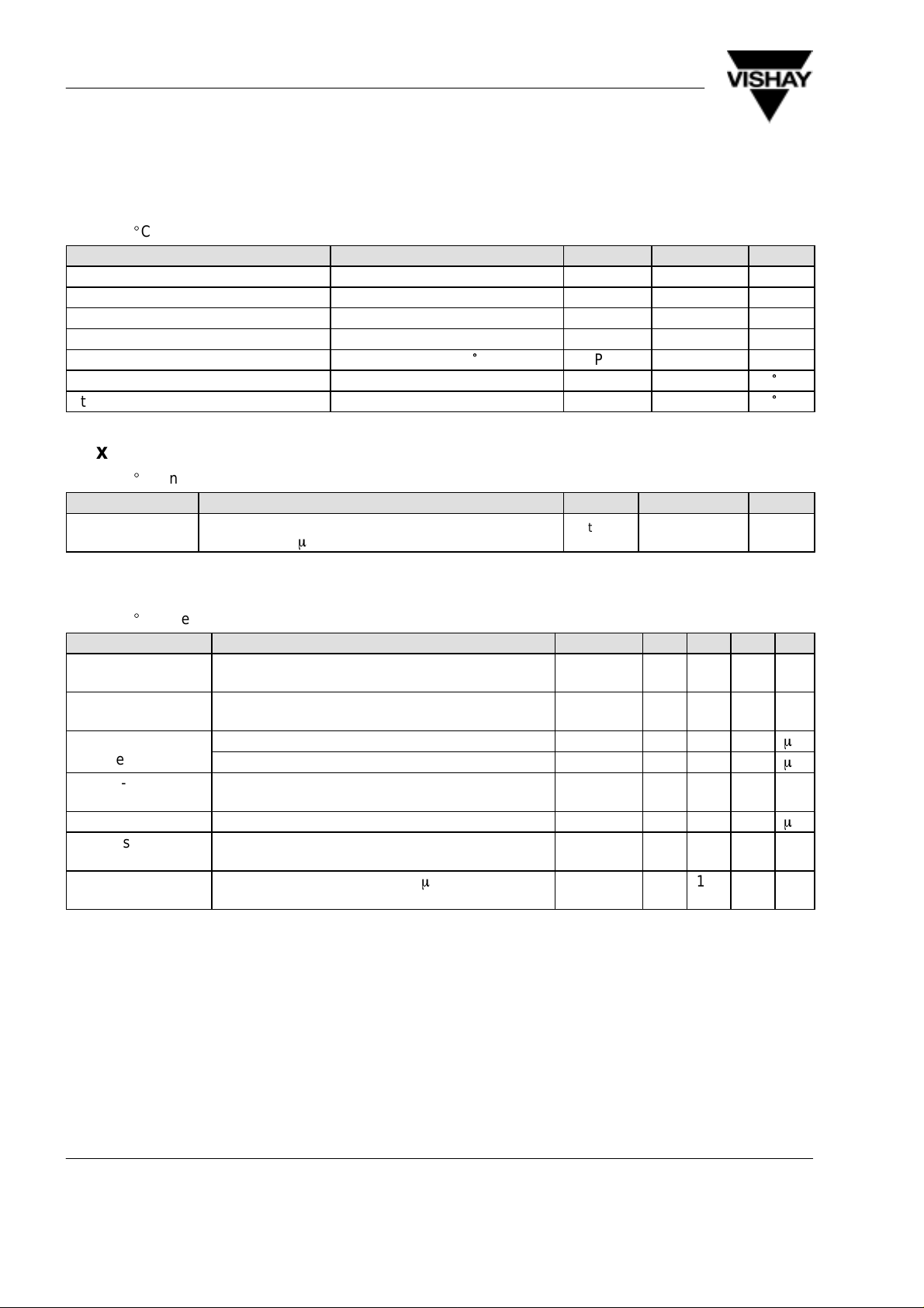
Absolute Maximum Ratings
T
= 25_C, unless otherwise specified
amb
Parameter Test Conditions Symbol Value Unit
Drain - source voltage V
Drain current I
Gate 1/Gate 2 - source peak current ±I
Gate 1/Gate 2 - source voltage ±V
Total power dissipation T
≤ 60 °C P
amb
Channel temperature T
Storage temperature range T
DS
D
G1/G2SM
G1/G2SM
tot
Ch
stg
Maximum Thermal Resistance
T
= 25_C, unless otherwise specified
amb
Parameter T est Conditions Symbol Value Unit
Channel ambient on glass fibre printed board (25 x 20 x 1.5) mm
plated with 35mm Cu
3
R
thChA
8 V
30 mA
10 mA
6 V
200 mW
150
–55 to +150
450 K/W
°
C
°
C
Electrical DC Characteristics
T
= 25_C, unless otherwise specified
amb
Parameter Test Conditions Symbol Min Typ Max Unit
Gate 1 - source
breakdown voltage
Gate 2 - source
breakdown voltage
Gate 1 - source +V
leakage current
Gate 2 - source
leakage current
Drain current VDS = 5 V, V
Self-biased
operating current
Gate 2 - source
cut-off voltage
±I
= 10 mA, V
G1S
±I
= 10 mA, V
G2S
= 5 V, V
G1S
–V
= 5 V, V
G1S
±V
= 5 V, V
G2S
VDS = 5 V, V
VDS = 5 V, V
= VDS = 0 ±V
G2S
= VDS = 0 ±V
G1S
= VDS = 0 +I
G2S
= VDS = 0 –I
G2S
= VDS = 0 ±I
G1S
= 0, V
G1S
= nc, V
G1S
= nc, ID = 20 mA V
G1S
= 4 V I
G2S
= 4 V I
G2S
(BR)G1SS
(BR)G2SS
G1SS
G1SS
G2SS
DSS
DSP
G2S(OFF)
7 10 V
7 10 V
50 500mA
9 13 18 mA
1.0 V
50
m
100mA
20 nA
A
www.vishay.de • FaxBack +1-408-970-5600
2 (5)
Document Number 85071
Rev. 3, 16-Mar-99
 Loading...