


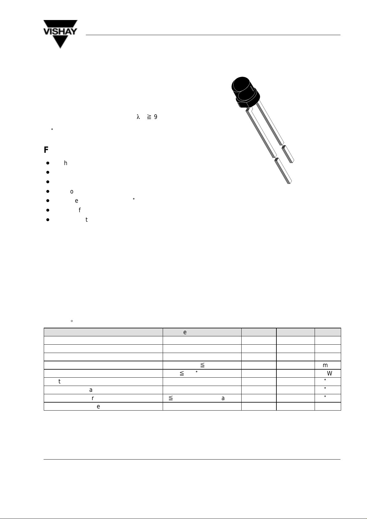
Silicon NPN Phototransistor
Description
TEFT4300 is a high speed and high sensitive silicon
NPN epitaxial planar phototransistor in a standard T–1
(ø 3 mm) plastic package.
The epoxy package itself is an IR filter, spectrally
matched to GaAs IR emitters with l
The plastic lens provides a wide viewing angle of ±
30°.
Features
D
High radiant sensitivity
D
Fast response times
D
T1 (ø 3 mm) plastic package with IR filter
D
Additional polarity sign
D
Wide viewing angle ϕ = ± 30
D
Suitable for near infrared radiation
D
Matches with TSUS4300 GaAs infrared emitter
y 900nm).
p
°
TEFT4300
Vishay Telefunken
94 8637
Applications
Optical switches
Counters and sorters
Interrupters
Tape and card readers
Encoders
Position sensors
Absolute Maximum Ratings
T
= 25_C
amb
Parameter Test Conditions Symbol Value Unit
Collector Emitter Voltage V
Emitter Collector Voltage V
Collector Current I
Peak Collector Current
Total Power Dissipation
Junction Temperature T
Storage Temperature Range T
Soldering Temperature
Thermal Resistance Junction/Ambient R
tp/T = 0.5, tp x 10 ms
T
x 55 °C
amb
t x 3 s, 2 mm from case
CEO
ECO
C
I
CM
P
tot
stg
T
sd
thJA
70 V
5 V
50 mA
100 mA
100 mW
j
100
–55...+100
260
450 K/W
°
C
°
C
°
C
Document Number 81549
Rev. 2, 20-May-99
www.vishay.de • FaxBack +1-408-970-5600
1 (5)
TEFT4300
Vishay Telefunken
Basic Characteristics
T
= 25_C
amb
Parameter Test Conditions Symbol Min Typ Max Unit
Collector Emitter Breakdown
Voltage
Collector Dark Current VCE = 20 V, E = 0 I
Collector Emitter Capacitance VCE = 5 V, f = 1 MHz, E=0 C
Collector Light Current Ee = 1 mW/cm2,
Angle of Half Sensitivity ϕ ±30 deg
Wavelength of Peak Sensitivity
Range of Spectral Bandwidth
Collector Emitter Saturation
Voltage
Turn–On Time VS = 5 V, IC = 5 mA,
Turn–Off Time VS = 5 V, IC = 5 mA,
Cut–Off Frequency VS = 5 V, IC = 5 mA,
IC = 1 mA V
l
= 950 nm, VCE = 5 V
Ee = 1 mW/cm2,
l
= 950 nm, IC = 0.1 mA
RL = 100
RL = 100
R
= 100
L
W
W
W
(BR)CE
O
CEO
CEO
I
ca
l
p
l
0.5
V
CEsat
t
on
t
off
f
c
70 V
1 200 nA
3 pF
0.8 3.2 mA
925 nm
875...1000 nm
0.3 V
2.0
2.3
180 kHz
m
s
m
s
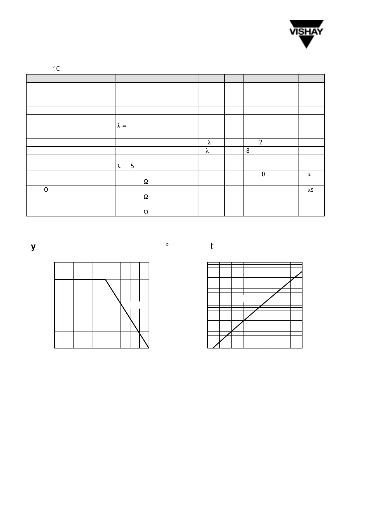
Typical Characteristics (T
125
100
75
50
25
tot
P – Total Power Dissipation ( mW )
0
020406080
T
94 8308
Figure 1. Total Power Dissipation vs.
– Ambient Temperature ( °C )
amb
Ambient Temperature
= 25_C unless otherwise specified)
amb
4
10
3
10
VCE=20V
40 60 80
T
– Ambient Temperature ( °C )
amb
CEO
I – Collector Dark Current ( nA )
94 8304
2
10
1
10
0
10
20
R
thJA
100
Figure 2. Collector Dark Current vs. Ambient Temperature
100
www.vishay.de • FaxBack +1-408-970-5600
2 (5) Rev. 2, 20-May-99
Document Number 81549