

Page 1

xx
TSG4100A Series
ZZZ
RF Signal Generators
User Manual
*P071315002*
071-3150-02
Page 2

Page 3

xx
TSG4100A Series
ZZZ
RF Signal Generators
User Manual
Register now!
Click the following link to protect your product.
► www.tektronix.com/register
www.tek.com
071-3150-02
Page 4

Copyright © Tektronix. All rights reserved. Licensed software products are owned by Tektronix or its subsidiaries
or suppliers, and are protected by national copyright laws and international treaty provisions.
Tektronix products are covered by U.S. and foreign patents, issued and pending. Information in this publication
supersedes that in all previously published material. Specifications and price change privileges reserved.
TEKTRONIX and TEK are registered trademarks of Tektronix, Inc.
Contacting Tektronix
Tektronix, Inc.
14150 SW Karl Braun Drive
P.O. B o x 5 0 0
Beaverto
USA
For product information, sales, service, and technical support:
n, OR 97077
In North America, call 1-800-833-9200.
Worldwide, visit www.tek.com to find contacts in your area.
Page 5

Table of Contents
Important safety information......... ................................ ................................ ............. v
General safety summary ...................................................................................... v
Service safety summary............ ................................ .................................. ....... vii
Terms in this manual ................. ................................ .................................. ..... viii
Symbols and terms on the product......................................................................... viii
Preface .............................................................................................................. ix
Key features ......... ................................ .................................. ........................ ix
Documentation................................................................................................. x
Software upgrades ............................................................................................ xi
Conventions used in this manual.................................... .................................. ...... xi
Installation........................................................................................................... 1
Before installation ............................................................................................. 1
Standard accessories.............................. .................................. ........................... 1
Optional accessories.......... .................................. ................................ ............... 2
Instrument options ...................... ................................ ................................ ....... 2
Connect to a network......... ................................ .................................. ............... 3
Upgrade the firmware through the USB port ............................................................... 6
Powering on the instrument................................................................................... 7
Powering off the instrument .................................................................................. 7
Removing power from the instrument....................................................................... 7
Inspecting the instrument .. ................................ .................................. ................. 8
Instrument maintenance....................................................................................... 9
Operating basics ... .................................. ................................ .............................. 10
Front panel controls ........................ .................................. ................................ 10
Connectors..................................................................................................... 11
Display, navigation, and menus ............................................................................. 15
Quick start and functional check.... .................................. ................................ ...... 23
Settings. ..... . ..... . ..... . ..... . .... . . ...... . ..... . ..... . ..... . ..... . ..... . ..... . ..... . ..... . . .... . . .... . . ... . . . 27
Presets.................................... ................................ .................................. .... 28
Modulation sources....... ................................ ................................ .................... 30
Error log ....................................................................................................... 36
Digital communications........................................................................................... 37
Introduction.................................................................................................... 37
Vector modulation ............................................................................................ 38
Modulation techniques ..... .................................. ................................ ................ 45
Specialized PSK constellations.................... .................................. ........................ 52
Modulation functions......................................................................................... 55
User waveforms, constellations, and filters..................................................................... 57
Downloading binary data .................................................................................... 57
TSG4100A Series RF Signal Generators User Manual i
Page 6

Table of Contents
Using the file As
Arbitrary user waveforms.................................................................................... 66
User constellations.................................... ................................ ........................ 67
User filters ..................................................................................................... 69
Reference ......................... ................................ ................................ .................. 71
Phase noise and offset diagrams ............................................................................ 71
Index
sistant utility software ..... . ..... . ..... . ..... . ..... . ..... . ... . . . .... . . .... . ..... . ..... . ... 58
ii TSG4100A Series RF Signal Generators User Manual
Page 7

List of Figures
Figure 1: Error vector magnitude.... ................................ .................................. .......... 45
Figure 2: ASK constellations .. ................................ ................................ .................. 46
Figure 3: FSK constellations ..................................................................................... 46
Figure 4: Fo
Figure 5: Phase trellis diagram for binary CPM with a rectangular filter ... ................................ 49
Figure 6: Constellations for QAM 4 through QAM 256 .................. ................................ .... 50
Figure 7: VSB symbol constellations ........................................................................... 51
Figure 8: Decoding DQPSK transmissions....................... ................................ .............. 52
Figure 9: Offset modulation prevents transitions through the origin ..... . ..... . ..... . ... . . . .... . . .... . . .... 53
Figure 1
Figure 11: 3π/8 8 PSK follows standard 8 PSK, but the constellation rotates by 3π/8 after each symbol 54
Figure 12: Architecture for mapping digital symbols into IQ constellation points ........................ 67
Figure 13: QPSK,3.840Mcps, 1.85 GHz, 0dBm), RMS EVM: 1.7% ....................................... 72
Figure 14: Image 2, QPSK,3.840Mcps, 1.85 GHz, 0dBm), RMS EVM: 1.7% ............................ 73
Figure 15: Option VM03 W-CDMA, (QPSK,3.840Mcps, 2.1425GHz, 0dBm), RMS EVM: 1.7% . .... 74
re 16: Image 2, Option VM03 W-CDMA, (QPSK,3.840Mcps, 2.1425GHz, 0dBm), RMS EVM:
Figu
1.7% .......................... ................................ .................................. ................ 75
Figure 17: Option VM04 APCO-25, (4FSK-C4FM,4.8KS/s,850MHz, 0dBm), Freq Err: 0.5%. . ..... . . 76
Figure 18: Option VM05 DECT, (2FSK1.152Mbps,1.925GHz, 0dBm), RMS FSK Err: 1.5% . ..... . ... 77
Figure 19: Option VM06 NADC, (π/4 DQPSK,24.3KS/s,875MHz, 0dBm), RMS EVM: 0.3%......... 78
Figure 20: Option VM07 PDC, (π/4 DQPSK,21KS/s, 800MHz,0dBm), RMS EVM: 0.6% ............. 79
gure 21: Option VM08 TETRA, (π/4 DQPSK,18KS/s, 420MHz, 0dBm), RMS EVM: 0.7% . .... . ... 80
Fi
ur basic PSK constellations........................ ................................ ................ 48
0: π/4 DQPSK uses differential encoding and a rotating constellation. ........................... 54
TSG4100A Series RF Signal Generators User Manual iii
Page 8

Table of Contents
List of Tables
Table 1: Front panel connectors.............. ................................ ................................ .... 12
Table 2: Rea
Table 3: Menus .............. ................................ .................................. .................... 16
Table 4: Preset default settings................................................................................... 24
Table 5: Modulation presets...................................................................................... 29
Table 6: TSG4102A and 4104A FM modulation vs. frequency ... .................................. ........ 34
Table 7: TSG4106A FM modulation vs. frequency ............... ................................ ............ 34
Table 8: V
Table 9: PSK constellations .......... ................................ .................................. .......... 47
Table 10: PRBS generating polynomials ..................... .................................. ................ 55
Table 11: Arbitrary waveform configuration word ............................................................ 66
Table 12: QPSK constellation point computations ........................ ................................ .... 69
r panel connectors .................... ................................ .............................. 13
ector phase modulation waveforms ................................................................. 47
iv TSG4100A Series RF Signal Generators User Manual
Page 9

Important safety information
This manual contains information and warnings that must be followed by the user
for safe operation and to keep the product in a safe condition.
To safely perform service on this product, additional information is provided at
the end of this section. (See page vii, Service safety summary.)
General safety summary
Use the product only as specified. Revie
avoid injury and prevent damage to this product or any products connected to it.
Carefully read all instructions. Retain these instructions for future reference.
Comply with local and national safety codes.
For correct and safe operation of the product, it is essential that you follow
generally accepted safety procedures in addition to the safety precautions specified
in this manual.
The product is designed to be used by trained personnel only.
Only qualified personnel who are aware of the hazards involved should remove
the cover for repair, maintenance, or adjustment.
Before use, always check the product with a known source to be sure it is
operating correctly.
This product is not intended for detection of hazardous voltages.
Use personal protective equipment to prevent shock and arc blast injury where
hazardous live conductors are exposed.
While using this product, you may need to access other parts of a larger system.
Read the safety sections of the other component manuals for warnings and
cautions related to operating the system.
w the following safety precautions to
When incorporating this equipment into a system, the safety of that system is the
responsibility of the assembler of the system.
To avoid fire or personal
injury
TSG4100A Series RF Signal Generators User Manual v
Use proper power cord. Use only the power cord specified for this product and
certified for the country of use.
Do not use the provided power cord for other products.
Ground the product. This product is grounded through the grounding conductor
of the power cord. To avoid electric shock, the grounding conductor must be
connected to earth ground. Before making connections to the input or output
terminals of the product, make sure that the product is properly grounded.
Do not disable the power cord grounding connection.
Page 10

Important safety information
Power disconne
source. See instructions for the location. Do not position the equipment so that
it is difficult to operate the power cord; it must remain accessible to the user at
all times to allow for quick disconnection if needed.
Observe all terminal ratings. To avoid fire or shock hazard, observe all ratings
and markings on the product. Consult the product manual for further ratings
information before making connections to the product. Do not exceed the
Measurement Category (CAT) rating and voltage or current rating of the lowest
rated individual component of a product, probe, or accessory. Use caution when
using 1:1 test leads because the probe tip voltage is directly transmitted to the
product.
Do not apply a potential to any terminal, including the common terminal, that
exceeds the maximum rating of that terminal.
Do not float the common terminal above the rated voltage for that terminal.
The measuring terminals on this product are not rated for connection to mains or
Category II, III, or IV circuits.
Do not operate without covers. Do not operate this product with covers or panels
removed, or with the case open. Hazardous voltage exposure is possible.
Avoid exposed circuitry. Do not touch exposed connections and components
when power is present.
ct. The power cord disconnects the product from the power
Do not operate with suspected failures. If you suspect that there is damage to this
product, have it inspected by qualifie
Disable the product if it is damaged. Do not use the product if it is damaged
or operates incorrectly. If in doubt about safety of the product, turn it off and
disconnect the power cord. Clearly mark the product to prevent its further
operation.
Examine the exterior of the product before you use it. Look for cracks or missing
pieces.
Use only specified replacement parts.
Use proper fuse. Useonlythefusetypeandratingspecified for this product.
Wear eye protection. Wear eye protection if exposure to high-intensity rays or
laser radiation exists.
Do not operate in wet/damp conditions. Be aware that condensation may occur if
a unit is moved from a cold to a warm environment.
Do not operate in an explosive atmosphere.
Keep product surfaces clean and dry. Remove the input signals before you clean
the product.
d service personnel.
vi TSG4100A Series RF Signal Generators User Manual
Page 11

Important safety information
Provide proper
details on installing the product so it has proper ventilation.
Slots and open
otherwise obstructed. Do not push objects into any of the openings.
Provide a safe working environment. Always place the product in a location
convenient for viewing the display and indicators.
Avoid improper or prolonged use of keyboards, pointers, and button pads.
Improper or prolonged keyboard or pointer use may result in serious injury.
Be sure your work area meets applicable ergonomic standards. Consult with an
ergonomics professional to avoid stress injuries.
Use only the Tektronix rackmount hardware specified for this product.
Servicesafetysummary
The Service safety summary section contains additional information required to
safely perform service on the p roduct. Only qualified personnel should perform
service procedures. Read this Service safety summary and the General safety
summa
ventilation. Refer to the installation instructions in the manual for
ings are provided for ventilation and should never be covered or
ry before performing any service procedures.
To avoid electric shock. Do not touch exposed connections.
Do not service alone. Do not perform internal service or adjustments of this
product unless another person capable of rendering first aid and resuscitation is
sent.
pre
Disconnect power. To avoid electric shock, switch off the product power and
disconnect the power cord from the mains power before removing any covers or
panels, or opening the case for servicing.
se care when servicing with power on. Dangerous voltages or currents may exist
U
in this product. Disconnect power, remove battery (if applicable), and disconnect
test leads before removing protective panels, soldering, or replacing components.
Verify safety after repair. Always recheck ground continuity and mains dielectric
strength after performing a repair.
TSG4100A Series RF Signal Generators User Manual vii
Page 12
Important safety information
Termsinthismanual
These terms may appear in this manual:
WARNING. Warning statements identify conditions or practices that could result
in injury or loss of life.
CAUTION. Caution statements identify conditions or practices that could result in
damage to this product or other property.
Symbols and terms on the product
These ter
The following symbol(s) may appear on the product:
ms may appear on the product:
DANGER indicates an injury hazard immediately accessible as you read
the mark
WARNING indicates an injury hazard not immediately accessible as you
read th
CAUTION indicates a hazard to property including the product.
ing.
e marking.
When this symbol is marked on the product, be sure to consult the manual
to find out the nature of the potential hazards and any actions which have to
betakentoavoidthem. (Thissymbolmayalsobeusedtorefertheuserto
ratings in the manual.)
viii TSG4100A Series RF Signal Generators User Manual
Page 13

Preface
Preface
Key features
This manual d
the TSG4100A Series RF Signal Generators. This manual supports the following
instruments
TSG4102A
TSG4104A
TSG4106A
NOTE. Che
more information about your product. Visit www.tektronix.com/manuals.
For comp
RF Signal Generators Installation and Safety Instructions that shipped with
your instrument. The document can also found on the Tektronix Web site at
www.tektronix.com/manuals.
The TSG4100A Series RF Signal Generators provide waveform generation and
support both analog (standard) and vector/digital (optional) modulation. The
instruments use a new technique to provide spurious free outputs with low phase
se (-113 dBc/Hz at20 KHz offset from 1 GHz carrier) and extraordinary
noi
frequency resolution (1 μHz at any frequency). An ovenized SC-cut oscillator
(M00 or E1 optioned m odels) timebase provides 100 times improvement in
stability (and a 100 times reduction in the in-close phase noise) compared to
instruments that use a TCXO time-base. Key features include:
escribes the installation, operation, and related signal concepts of
ck the Tektronix Web site for updates to this manual, which will include
liance, environmental, and safety information, see the TSG4100A Series
TrueDCto2GHz,4GHz,or6GHz
Typical ±0.30 dB amplitude accuracy (0 dBm CW signal at 22 ºC) from
100 MHz to 6 GHz
Dual baseband ARB generators
Analog modulation
Soft key to vector modulation upgrade
I/Q modulation inputs (400 MHz RF BW)
ASK, FSK, MSK, PSK, QAM, VSB, and custom I/Q
TSG4100A Series RF Signal Generators User Manual ix
Page 14

Preface
Digital modula
tion applications for GSM, EDGE, W-CDMA, APCO-25,
DECT, NADC, PDC, and TETRA
USB, GPIB, RS-
232 and LAN interfaces
Documentation
The followi
Signal Generator. The product documentation CD provided contains documents
available at the time of publication. For the most current documentation, refer to
the Tektronix Web site at www.tektronix.com/manuals.
To read about Use these documents
Basic installation, safety, and compliance Installation and Safety Instructions
Operation and installation User Manual (this manual)
Programming commands Programmer Manual
Specifications and
performance verification
User service
Data security
ng documentation is available for your Tektronix TSG4100A Series RF
This document contains basic information about instrument connectors, how
to turn it on and off, compliance, environmental, and safety information. This
manual is shipped as a printed book with your product and provides information
in English and Russian. It is also available as a PDF file, downloadable from
www.tektronix.com/manuals.
The user manual contains information about how to navigate the instrument UI,
how to operate the instrument, and information about signals. This manual is
available in printed form in English or Russian. Both are also available as PDF
files.
This manual contains descriptions of programming commands and their use.
This manual is available as a PDF file.
Specifications and Performance Verification Manual
This manual contains the instrument specifications and a procedure to check
instrument performance against warranted characteristics. This manual is
available as a PDF file.
Service Manual
This manual provides a list of replaceable parts, care and maintenance
information, and information for servicing the instrument to the module level.
This manual is available as a PDF file.
Declassification and Security Instructions
This document helps customers with data security concerns to sanitize or
remove memory devices. This document is available as a PDF file.
x TSG4100A Series RF Signal Generators User Manual
Page 15
Preface
Software upgr
Conventi
onsusedinthismanual
ades
Software option upgrades are available. Software upgrades for options become
operational only after you enter a valid option key for the specific generator model
and serial nu
To check for upgrade s:
1. Use your Web browser to go to www.tektronix.com/software.
2. Enter the product name (for example TSG4104A) to find available software
upgrades.
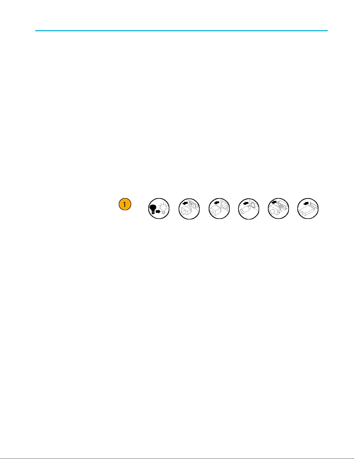
The following icons are used throughout this manual:
Sequence
Step
mber.
Front
panel
power
Connect
power
Network
PS2 SVGA USB
TSG4100A Series RF Signal Generators User Manual xi
Page 16

Preface
xii TSG4100A Series RF Signal Generators User Manual
Page 17

Installation
Before installation
Standard accessories
Unpack the instrument, and check that you received all items listed as Standard
Accessories. Optional accessories and instrument options are also listed in this
section. Check the Tektronix Web site (www.tektronix.com) for the most current
information.
Your instrument comes with the following accessories: installation and safety
instructions (English and Russian languages), product software and documentation
CD, and power cord.
Documents
Software
RF cable
Power cords
TSG4100A Series RF Signal Generators Installation and Safety Instructions
is a multi-language document (English and Russian). Tektronix part number
071-3390-XX.
TSG4100A Series RF Signal Generators Product SW and Documentation CD,
Tektronix part number 063-4557-XX.
TSG File Assistant is a software application that allows you to convert raw data
of custom waveforms, constellations, and filters (*.txt or *.csv files) to *.tsw,
*.tsf, and *tsc files that are supported by the TSG. This software is available
on the SW and Documentation CD that shipped with the instrument and for
download from the Tektronix Web site at www.tektronix.com
NOTE. You can read more about how the TSG File Assistant works in this manual.
RF cable (Tektronix part number 012-1738-00): 1 meter, 50 Ω,N-typeto
N-type
The TSG4100A Series RF Sig
power cord options. Power cords for use in North America are UL listed and CSA
certified. Cords for use in areas other than North Americ a are approved by at lea st
one authority acceptable in the country to which the product is shipped.
nal Generators are shipped with one of the following
/downloads.
Opt. A0 - North America power
Opt. A1 - Universal EURO power
Opt. A2 - United Kingdom power
Opt. A3 - Australia power
TSG4100A Series RF Signal Generators User Manual 1
Page 18

Installation
Optional accessories
Opt. A5 - Switze
Opt. A6 - Japan power
Opt. A10 - China power
Opt. A11 - India power
Opt. A12 - Brazil power
Opt. A99 - No power cord
Option TSG4100A-RM1; Single rackmount kit for all TSG4100A models
Option TS
Option TSG4100A-ATT: 30 dB, 5 Watt RF attenuator up to 6 GHz
Option GPIB: Adds GPIB interface
Option D1: A list of performance verification test results
Option L0: Printed User manual (this manual). English. (You can always
download an English or Russian User manual from the Tektronix Web site at
www.tektronix.com/manuals.)
G4100A-RM2: Dual rackmount kit for all TSG4100A models
rland power
rument options
Inst
The following options must be specified at time of instrument order.
regions except North America. The following instrument configuration options
All
are available in all regions except North America.
0: Instrument with oven-controlled crystal oscillator (OCXO).
M0
M01: Instrument with voltage-controlled crystal oscillator (VCXO).
GPIB: Adds GPIB interface.
2 TSG4100A Series RF Signal Generators User Manual
Page 19

Installation
Software options
North A merica o
only in North America.
E1: Instrumen
and GPIB interface.
You can add the following software options to your generator:
Option VM00: Basic vector modulation package with internal 6M Hz
modulation bandwidth
Option VM01: GSM modulation (requires Option VM00)
Option VM
Option VM03: W-CDMA modulation (requires Option VM00)
Option VM04: APCO-25 modulation (requires Option VM00)
Option VM05: DECT modulation (requires Option VM00)
Option VM06: NADC modulation (requires Option VM00)
Option VM07: PDC modulation (requires Option VM00)
Optio
nly. The following instrument configuration option is available
t with oven-controlled crystal oscillator (OCXO) time-base
02: GSM EDGE modulation (requires Option VM00)
n VM08: TETRA modulation (requires Option VM00)
Connect to a network
LAN interface
Option VM10: Audio c lip (analog AM and FM) (requires Option VM00)
Option EIQ; External 200 MHz modulation bandwidth (requires Option
VM00)
You can communicate with or remotely control your instrument through the LAN,
232, or GPIB interfaces. (GPIB requires Option GPIB.)
RS
The LAN connector may be used to connect the instrument to a 10/100 Base-T
Ethernet LAN. Before connecting the instrument to your LAN, check with your
etwork administrator for the proper method of configuration of instruments
n
on your network.
To set up the LAN interface:
1. Connect a LAN cable to the rear panel LAN port.
2. Press the Utility button from the main menu.
3. Select I/O Interface.
4. Select LAN to view the Ethernet network settings.
TSG4100A Series RF Signal Generators User Manual 3
Page 20
Installation
5. Use the menu but
other network information.
By selecting t
automatically through DHCP. If you cannot establish communication using
DHCP, you need to manually set up an IP address and a Subnet Mask, if
necessary.
6. Press the Enter button.
7. Press the Return button three times to return to the main menu.
TCP/IP configuration methods. InordertofunctionproperlyonanEthernet
based local area network (LAN), the unit needs to obtain a valid IP address, a
subnet mask, and a default gateway or router address. There are three methods
for obta
network administrator for the proper method of configuration of instruments
on your network.
TCP/IP based remote interfaces. Three TCP/IP based remote interfaces are
supported: raw socket, telnet, and VXI-11 net instrument. Raw socket access is
avail
interface enables IEEE 488.2 GPIB-like access to the unit over TCP/IP. It enables
controlled reads and writes and the ability to generate service requests. Most
recent VISA instrument software libraries support this protocol.
ining these parameters: DHCP, Auto-IP, and Static IP. Check with your
able on port 5025. Telnet access is available on port 5024. The VXI-11
tons and number keys to enter the desired IP address and
he DHCP ON, the instrument can set its network address
Link speed. The physical Ethernet layer supports 10 Base-T and 100 Base-T link
eds. The default link speed is set to 100 Base-T, but it can be set to 10 Base-T.
spe
To reset the TCP/IP interface. When configured from the front panel, the TCP/IP
is automatically reset. Otherwise, changes to the TCP/IP configuration do not take
effect until the TCP/IP interface is either reset or the instrument power is cycled.
When reset is selected, any active connections will be aborted. The TCP/IP stack
ill be reinitialized and configured using the latest configuration options.
w
CAUTION. Network security is an important consideration for all TCP/IP
networks. This instrument does not provide security controls, such as passwords
or encryption, for controlling access. If such c ontrols are needed, you must
provide it at the network level. For example, you can use an internet firewall.
4 TSG4100A Series RF Signal Generators User Manual
Page 21

Installation
GPIB interface
The GPIB connec
supports the required common commands of the IEEE-488.2 (1987) standard.
NOTE. Changes to the GPIB configuration do not take effect until the interface is
reset or the instrument power is cycled.
To set up the GPIB interface:
1. Connect a GPIB cable to the rear panel GPIB port.
2. Press the U
3. Select I/O Interface.
4. Select GPIB.
5. Check that GPIB is set to ON. If it is not, highlight ON in the GPIB menu
to turn it on.
6. Press the Address button and use the number keys to assign a unique address
to the instrument.
NOTE. Each device connected to the GPIB bus must have a unique GPIB address.
The GP
IB address must be from 0 to 30.
tor supports the IEEE-488.1 (1978) interface standard. It also
tility button from the main menu.
RS-232 interface
7. Press the Enter button.
8. Press the Return button three times to return to the main menu.
The RS-232 interface connector is a standard 9 pin, type D, female connector
configured as a DCE (transmit on pin 2, receive on pin 3). In order to communicate
properly over RS-232, the instrument and the host computer both m ust be set up
tousethesameconfiguration. The following baud rates are supported: 115200
default), 57600, 38400, 19200, 9600, and 4800. The rest of the communication
(
parameters are fi xed at 8 data bits, 1 stop bit, no parity, and RTS/CTS hardware
flow control.
To set up the RS-232 interface:
1. Connect a cable to the rear panel RS-232 port. Use a cable best suited for the
desired baud rate (modulation rate).
2. Press the Utility button from the main menu.
3. Select I/O Interface.
4. Select RS232.
TSG4100A Series RF Signal Generators User Manual 5
Page 22

Installation
5. Check that RS23
to turn it on.
6. Press the Baud
rate.
7. Press the Re
2issettoON. If it is not, highlight ON in the RS-232 menu
Rate button and turn the general knob to set the desired baud
turn button three times to return to the main menu.
Upgrade the firmware through the USB port
The USB por
memory device. To upgrade the firmware using the USB port, do the following:
1. From a com
most recent instrument firmware from the Tektronix Web site at
www.tektronix.com/downloads onto a USB memory device. Note the
firmware version.
2. Press the Utility button from the instrument main menu.
3. Select System > About.
4. Look at
shown is older than the firmware version you downloaded from the Tektronix
We b site.
t allows you to upgrade the instrument firmware using a USB
puter with an internet connection, download the
the instrument display screen and v erify that the firmware version
5. Insert the USB memory device into the USB port on the front panel of the
instrument.
6. Check that the Firmware Update menu option becomes active a fter
approximately 10 seconds as the instrument recognizes the USB memory
device.
7. Press the Firmware Update button. A dialog box will appear asking if you
want to update the firmware.
8. Use the arrow k eys to highlight Ye s if you want to start the update process, or
No if you want to cancel the process.
9. Press the Enter button to start the update process (or cancel it if you selected
No).
6 TSG4100A Series RF Signal Generators User Manual
Page 23
Powering on the instrument
Installation
Powering o
Remov
ing power from the instrument
ff the instrument
TSG4100A Series RF Signal Generators User Manual 7
Page 24

Installation
Inspecting the instrument
Run the Self Test (Utility > System > Self Test) to run a series of tests to verify that
the instrument is operating correctly. It tests communication to various peripherals
on the main board, including the GPIB chips, the PLL chips, the DDS chips, the
octal DACs, the FPGA, and the serial EEPROM. Errors will be reported on the
front-pane
error buffer and may be accessed through the e rror status menu after the self test
completes. See section Error Codes on page 126 for a complete list of error codes.
If you want to check the accuracy specifications of your instrument, see the
TSG4100A Series RF Signal Generators Specifications and Performance
Verification Technical Reference PDF available on the Tektronix Web site at
www.tektronix.com/manuals.
l display when detected. The errors detected are stored in the instrument
8 TSG4100A Series RF Signal Generators User Manual
Page 25
Instrument maintenance
Installation
Clean your in strument
Clean the exterior surfaces of the chassis with a dry lint-free cloth or a soft-bristle
brush. If any dirt remains, use a cloth or swab dipped in a 75% isopropyl alcohol
solution. Use a swab to clean narrow spaces around controls and connectors. Do
not use abrasive compounds on any part of the instrument because they might
damage the i
CAUTION. Avoid getting moisture inside the instrument during exterior cleaning;
use just enough moisture to dampen the cloth or swab. Do not wash the
front-panel On/Off button. Cover the button while washing the instrument. U se
only deionized or distilled water when cleaning. Use a 75% isopropyl alcohol
solution as a cleanser and rinse with deionized or distilled water. Do not use
chemica
contain benzene, toluene, xylene, acetone, or similar solvents.
CAUTIO
cleaning agents or methods. Avoid using abrasive cleaners or commercial glass
cleaners to clean the display surface. Avoid spraying liquids directly on the
display surface. Avoid sc rubbing the display with excessive force.
Clean the display surface by gently rubbing the display with a clean-room wipe. If
the display is very dirty, moisten the wipe with distilled water or a 75% isopropyl
alcohol solution and gently rub the display surface. Avoid using excess force;
this might damage the display surface.
nstrument.
l cleaning agents; they might damage the chassis. Avoid chemicals that
N. To prevent damage to the flat panel display, do not use improper
rade your instrument
Upg
Return your in strument
Software upgrades are available from Tektronix. They can either be downloaded
from the Tektronix Web site or they can be ordered from your local Tektronix
representative. To add additional software options or features, you will need an
ption key from Tektronix. When you receive the software from Tektronix, you
o
will also receive an option key. Follow the instructions you receive to install the
software on your instrument. You will be prompted to enter the option key. See
the About menu on the instrument to enter an option key. This information is in
the Menus section of this manual. (See page 16 , Menus.)
If you return your instrument to Tektronix:
When repacking the instrument for shipment, use the original packaging. If
the packaging is unavailable or unfit for use, contact your local Tektronix
representative to obtain new packaging.
Seal the shipping carton with an industrial stapler or strapping tape.
TSG4100A Series RF Signal Generators User Manual 9
Page 26
Operating basics
Operating bas
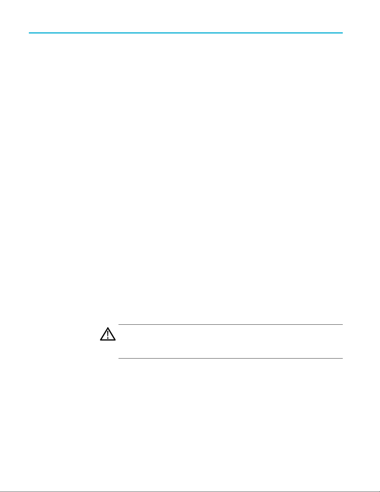
Front panel controls
ics
The followi
the controls and elements noted in the illustration.
ng illustration shows the instrument front panel. The table describes
Front panel
10 TSG4100A Series RF Signal Generators User Manual
Page 27
Operating basics
Item
number
1 Power button
2RF
3 Adjustment
4
5
6
7
8Freq
9Ampt Presst
10 Mod Press to access modulation menu.
11
12
13
14
15 Numeric keypad
16 Menu selection
Control element or
group Description
Press to turn power on or off. The power button has two modes: STANDBY and ON.
In STANDBY mod
consumption will not exceed 20 W once the instrument is warmed up. In ON mode, power
is supplied to all circuitry and the instrument is on.
Press to turn R F signal output ON (LED light on) or OFF (LED light off). Only outputs that
areactivef
minimum value it will be disabled and the LED light will turn off.
knob
Select key
Preset
Setting
Mod On/Off Press to turn modulation function ON or OFF.
G/n ( dBμV) Press to select units (GHz, ns, nv, dBμv).
M/μ (μV) Press to select units (MHz, μs, μv).
K/m (mV) Press to select units (KHz, ms, mv)
Enter (dB(m)) Press to select units (Hz, s, dBm).
buttons
s
Turn knob to
Press to en
underscore position when editing a parameter.
Press and hold to recall default setup.
Press to a
Press to adjust RF frequency.
o adjust amplitude.
Use these keys to enter numeric values for a variety of parameters.
Use these buttons to select menu items on the screen.
e, power is only supplied to the internal timebase and the power
or the current frequency setting will be accessible. If an output is set below its
navigate menus and adjust parameters.
ter submenu (right arrow), return to m ain menu (left arrow), or to adjust the
ccess the top menu.
Connectors
he following figures and tables show and describe various connectors located
T
on the front panel and rear panel of the instrument.
Front panel connectors
TSG4100A Series RF Signal Generators User Manual 11
Page 28

Operating basics
Table 1: Front p
anel connectors
Item
number Connector Description
1
LF Output BNC output. Active for frequency s ettings between DC and 62.5 MHz. The amplitude may
be set independently for levels from 1 μV
protected ag
2
RF Output Type N outpu
950 kHz and 4 GHz (TSG4104A), and 950kHz and 6 GHz (TSG4106A). The output power
may be set from −110 dBm to 16.5 dBm (0.7 μV
3
USB A USB connector allows you to connect an external memory device to the instrument for
data stora
ge.
RMS
to1V
(–47 dBm to 13 dBm). This output is
RMS
ainst externally applied voltages of up to ±5 V.
t. Active for frequency settings between 950 kHz and 2 GHz (TSG4102A),
RMS
to 1.5 V
RMS
).
12 TSG4100A Series RF Signal Generators User Manual
Page 29
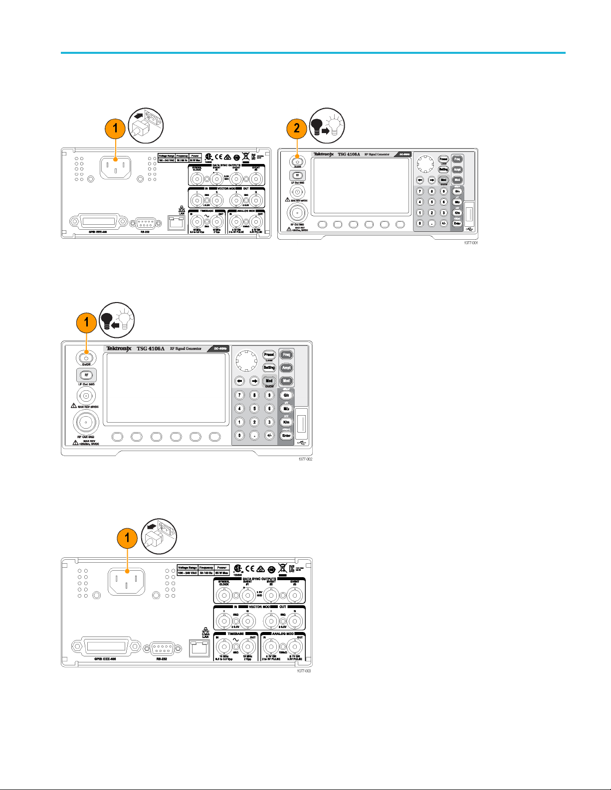
Rear panel connectors
Table 2: Rear panel connectors
Item Connector Description
1
2
3
4
5
6
AC power (input) Connect the unit to a power source through the power cord provided with the instrument.
The center pin is connected to the chassis so that the entire box is earth grounded. The
unit will operate with an AC input from 100 to 240 V
Hz. The instrument requires 85 W and implements power factor correction. Connect
only to a properly grounded outlet.
SYMBOL CLOCK
(output)
This BNC provides a square wave synchronized to the symbol clock used in the
modulation. The r ising edge of this clock triggers the programmed event markers
associated with the arbitrary waveform.
EVENT (outputs) Three BNC outputs labeled #1, #2, and #3 are available for synchronizing external
instrumentation to programmable events within a generated arbitrary waveform. These
may be programmed, for instance, to mark the start of a frame, or a slot within a frame,
or the start of a synchronizing pattern in the waveform. One of the event markers may be
further programmed to control the RF power of the front panel output for the generation
of TDMA signals. Events are triggered on the rising edge of the symbol clock.
VECTORMODINI
VECTOR MOD IN Q
These BNC inputs enable external I/Q modulation. They accept signals of ±0.5 V,
corresponding to full scale modulation, and have 50 Ω input impedances. Both inputs
support signal bandwidths from DC to 100 MHz providing an RF modulation bandwidth
of up to 200 MHz.
VECTOR MOD OUT I
VECTOR MOD OUT Q
These BNC outputs replicate the baseband I/Q modulation waveforms currently being
used to modulate the RF. Both outputs have a source impedance of 50 Ω and when
terminated into 50 Ω, will generate a full scale output of ±0.5 V.
ANALOG MOD OUT This output replicates the analog modulation waveform and has a 50 Ω reverse
termination. When using the internal source for AM, FM, and ΦM, it provides a waveform
determined by the function and rate settings with an amplitude of 1 V
impedance. During external analog modulation, this output mirrors the modulation
input. For Pulse modulation, the output is a 3.3 V logic waveform that coincides with
the gate signal.
Operating basics
, and with a frequency of 50/60
AC
into a high
PP
TSG4100A Series RF Signal Generators User Manual 13
Page 30

Operating basics
Table 2: Rear panel connectors (cont.)
Item Connector Description
7
8
9
10 LAN
11
12
ANALOG M OD IN External analog modulation is applied to this input. The input impedance is 100 kΩ with
a selectable input coupling of either DC or AC (4 Hz roll off). For analog modulations
(AM, FM, ΦM), a signal of ±1 V will produce a full scale modulation of the output (depth
for AM or deviation for FM and ΦM). It supports bandwidths of 100 kHz and introduces
distortions of less than –50 dB. For Pulse modulation types, this input is used as a
discriminator that has a fixed threshold of +1 V.
TIMEBASE OUT
(10MHz2V
)
pp
TIMEBASE IN (10 MHz
0.5 to 3.0 V
)
pp
The instrument also provides a 10 MHz output for referencing other instrumentation
to the internal timebase.
This input accepts an external 10 MHz reference. The external reference should be
accurate to at least 2 ppm, and provide a signal of no less than 0.5 VPPwhile driving
a50Ω impedance. The instrument automatically detects the presence of an external
reference and locks to it, if possible. If the unit is able to lock to the reference, this is
indicated on the front panel display.
The Ethernet uses a standard R J-45 connector to connect to a local area network (LAN)
using standard Category-5 or Category-6 cable. It supports both 10 and 100 Base-T
Ethernet connection and a variety of TCP/IP configuration methods.
RS-232 The RS-232 port uses a standard 9 pin, female, subminiature-D connector. It is
configured as a DCE and supports baud rates from 4.8 kb/s to 115 kb/s. The remaining
communication parameters are fixed at 8 Data bits, 1 Stop bit, No Parity, with RTS/CTS
configured to support H ardware Flow Control.
GPIB The GPIB (IEEE-488) communications port is for communications over a GPIB bus. T he
instruments support the IEEE-488.1 (1978) interface standard. It also supports the
required common commands of the IEEE-488.2 (1987) standard.
E. When EXT is selected as the Source, the instrument will look for an
NOT
external 10 MHz reference at the timebase input BNC. If detected, the instrument
will attempt to lock its internal clock to the external reference.
14 TSG4100A Series RF Signal Generators User Manual
Page 31

Display, navigation, and menus
Controls and display elements are shown in the following illustrations and tables.
Operating basics
Ref
number
1
2
3
4 Menus
Displayareafunction
Status
Quick
Settings Shows the parameters that can be modified for the currently selected item. You can
view
Display
The display s
Descrip
Indicates instrument status. When an item is highlighted yellow or is displayed with bold
typeface, that feature is active. This area shows m odulation types, and if Modulation and
RF are O
Shows
on the front panel.
modify a parameter by pressing the corresponding menu button and then using the arrow
keys
Menu
such as LAN or GPIB setup, or setting a particular modulation type. Use the arrow k eys,
general knob, and Enter key on the front panel to navigate the menus.
creen is divided into the following four sections:
tion
N or Off. Error messages, if applicable, show in the right corner of this area.
frequency and amplitude values. Units can be changed using the unit buttons
, general knob, and Enter key on the front panel.
buttons show items that you can select to access submenus for specific a ctions,
Saving display i mages
(screen shots)
You can save *.bmp files of the instrument display to a USB memory device as
follows:
1. Insert a USB memory device into the USB port on the front of the instrument.
et the display as desired.
2.S
3. Simultaneously press and hold the < and > keys for 1 second.
4. Remove the memory device and download the saved *.bmp files to your PC
or other device.
TSG4100A Series RF Signal Generators User Manual 15
Page 32

Operating basics
Navigation
Navigate the Me
nus and Settings areas of the display by using the arrow keys
(left, right), general knob (up, down, and push in knob to select), and Enter key
(select). When a parameter is selected in the Settings area, you can use the arrow
keys to select a digit, the number keys to enter a value, and the Enter key to make
a selection. When you are fi nished, press the Enter key to set the parameter and
then any menu item to deselect the parameter.
Menus
The following menus are available.
Table 3: Menus
Menu Description
Main menu
RF/LF menu and settings.
.
Mod m enu and settings.
Access modulation presets, constellation,
source, rate, filter and other submenus.
The menu options in this menu change
depending on the active modulation type.
16 TSG4100A Series RF Signal Generators User Manual
Page 33

Table 3: Menus (cont.)
Menu Description
Mod Type submenus: Analog, Vector, Presets.
Operating basics
Constellation menu.
This is a Mod submenu. It is available when
the appropriate modulation type is active. The
items in this menu vary depending on the active
modulation type.
TSG4100A Series RF Signal Generators User Manual 17
Page 34

Operating basics
Table 3: Menus (cont.)
Menu Description
Source menu.
This is a Mod submenu. It is available when
the appropriate modulation type is active. The
items in this m enu vary depending on the active
modulation type.
Filter menu.
This is a Mod submenu. It is available when
the appr
items in this m enu vary depending on the active
modulation type.
opriate modulation type is active. The
AWGN/IMP menu: Noise submenu and
AWGN/IMP settings.
Utility menu.
18 TSG4100A Series RF Signal Generators User Manual
Page 35

Table 3: Menus (cont.)
Menu Description
I/O Interface menu.
This is a Utility submenu.
RS232 menu and settings.
This is an I/O Interface submenu.
Operating basics
GPIB me
This is an I/O Interface submenu.
This requires the instrument have the GP IB
optio
nu and settings.
n.
TSG4100A Series RF Signal Generators User Manual 19
Page 36

Operating basics
Table 3: Menus (cont.)
Menu Description
LAN menu, submenus, and settings.
This is an I/O Interface submenu.
System menu.
This is a Utility submenu.
Allows you to set display backlight, date, time,
run a self test, and remove private data (Secure).
Secure setting.
This is a System menu action that allows you
to remove private data. Use the arrow keys to
select Yes or No and then press the general
knob or the Enter button on the front panel.
20 TSG4100A Series RF Signal Generators User Manual
Page 37

Table 3: Menus (cont.)
Menu Description
File menu.
This is a Utility submenu. It allows you to access
saved files such as waveform, constellation,
filter, and setup files. Available files will show in
the Settings area of the display when you select
the file type.
You can load a file from the USB to location 0 on
the instrument (USB), save a file (Save To) to
location 1 through 9, delete a file (Delete), and
delete all files (Erase All).
The Setup submenu allows you recall and save
setups (Recall).
Operating basics
Status menu.
This is a Utility submenu. It shows the status of
the instrument in the Settings area.
TSG4100A Series RF Signal Generators User Manual 21
Page 38

Operating basics
Table 3: Menus (cont.)
Menu Description
About menu.
This is a Utility submenu. It shows the instrument
firmware version, installed options, instrument
serial number in the Settings area.
License M anage menu.
This is an About submenu. It allows you to enter
option/software keys to activate options.
Firmware Update m enu.
This is an About submenu. It allows you to
upgrade the firmware using the USB port.
NOTE. Upgrade procedures are available in
this manual. (See page 6, Upgrade the firmware
through the USB port.)
22 TSG4100A Series RF Signal Generators User Manual
Page 39

Table 3: Menus (cont.)
Menu Description
USB menu.
This is a Utility submenu. It allows you to access
files from a USB memory device. Available files
show in the Settings area of the display.
Error code menu.
This is a Utility submenu. It is an error log and
allows you to view any error codes that have
appeared.
Operating basics
Quick start and functional check
ectionisintendedtohelpfirst time users get started using a Tektronix
This s
TSG4100A Series RF Signal Generator and to help verify that the instrument is
functioning correctly.
Turn on the instrument
1. Con
2. Pu
3. Ch
NOTE. Your instrument will resume operating with the same settings that were
active when it was last turned off. You can preset the instrument to a default state
without changing any of the stored settings or the communications configuration.
(See page 24, Set default settings (Preset button).)
nect the supplied power cord to the rear panel power input and then to the
AC mains power supply (100 to 240 V
sh the power button located on the left top corner of the front panel of the
instrument.
eck that the model number, firmware version, and instrument serial number
brieflydisplay.
±10%).
AC
TSG4100A Series RF Signal Generators User Manual 23
Page 40

Operating basics
Set default settings (Preset
button)
To set the instr
presets, press and hold the Preset button on the front panel for three seconds. The
ument to the factory default settings without affecting saved
following table shows some of the default settings that will be loaded.
Table 4: Preset default settings
Setting Default value
Frequency 10 MHz
Amplitude (BNC) 0 dBm (1 mW into 50 Ω or 0.63 V
Amplitude (Type N) 0 dBm (1 mW into 50 Ω or 0.63 V
Modulation
Modulation Type FM
RF
Source Sine
Rate 1 kHz
Deviation 1 kHz
Conne
ct outputs to
oscilloscope
1. Use appropriate cables to connect the front panel BNC and Type N outputs to
an oscilloscope.
OFF
ON
2. Set the oscilloscope timebase to 50 ns/div and vertical sensitivity for
200 mV/div with DC coupling and 50 Ω input impedance.
PP
PP
Basic functional check
3. Check that the displayed cycle period is 100 ns (2 divisions).
4. Check that the displayed amplitude is 630 mV
.
PP
NOTE. The displayed amplitude will be 630 mV if the oscilloscope input is not
set for 50 Ω.
Do the following after connecting to an oscilloscope to check that the information
shows as expected on the display screen and that you can adjust the parameters
and navigate the menus properly.
24 TSG4100A Series RF Signal Generators User Manual
Page 41

Operating basics
1. Change the freq
a. Press the Freq button on the front panel to select the Frequency parameter
in the Quick View area.
b. Press the 5 number key.
c. Press the M/μ button to set the units to MHz.
d. Press the Setting button to exit the frequency setting.
Navigation quick tip. You can se
units as follows: press the Freq button, use the general knob to increase/decrease
the value, and then press the Setting button.
2. Change the amplitude for the Type N output by 1 dBm as follow
a. Press the Ampt button on the front panel to select the Type-N output
amplitude parameter in the Quick View area.
b. Press the Enter button to set the units to dBm.
c. Use the general knob to increase the amplitude by 1 dBm.
d. Press the Setting button to set and exit the amplitude setting.
Navigation quick tip. You can use the number keys and unit keys to set the
amplitude parameter value and units as follows: press the Ampt button, press the
desired number key, press the desired unit key, and then press the Setting button.
uencyto5MHzasfollows:
t the frequency parameter without changing the
s:
Modulation presets
functional check
3. Change the amplitude for the BNC output by 0.001 V as follows:
a. Select RF/LF from the main menu.
b. Select LF Amplitude from the submenu.
c. Press the 5 number k ey.
d. Press a unit key to set the LF Amplitude to Vpp or Vrms.
e. Press the k/m button to set the units to mV.
f. Use the general knob to increase the amplitude by 1 mV.
g. Press the Setting button to set and exit the amplitude setting.
Your instrument includes a number of modulation presets that automatically
configure the generator to produce modulation waveforms for a number of
different communications protocols, such as GSM, DECT, and TETRA. Do the
following to see how this preset type is enabled.
1. Press the Freq button and then set the frequency to 935.2 MHz.
2. Select Mod from the Main menu.
3. Select Mod Type from the Mod submenu.
TSG4100A Series RF Signal Generators User Manual 25
Page 42

Operating basics
4. Use the general
NOTE. Turn the general knob to highlight your selection. Press the general
knob to select it.
5. Turn the general knob to highlight GSM andthenpresstheEnter button to
load the GSM preset.
6. Press the Mod On/Off button to enable modulation. The LED will be lit
and MODON will show in the Status area of the display when modulation
is on. The i
slot of random data.
7. Connect t
event ma rker #1.
8. Trigger
oscilloscope trace should look similar to that shown below.
the oscilloscope on event marker #1 and set the time/div to 10 μs. The
knob to select Preset from the Mod Type menu.
nstrument will generate a GSM frame consisting of one TDMA
he following to the oscilloscope: I/Q outputs, symbol clock, and
The oscilloscope traces above show that before the TDMA slot begins, the I
and Q outputs are at ground, indicating that the RF power is off. Two symbols
efore the beginning of the time slot, the power is ramped up to full power. The
b
beginning of data transmission for the time slot is indicated by event marker #1,
whichistrace4inthefigure. The symbol clock shows the timing of symbol
transmission relative to the I/Q outputs.
26 TSG4100A Series RF Signal Generators User Manual
Page 43

Settings
Operating basics
Frequency
Phase
Amplitude
Pressing the Freq button allows you to adjust the carrier frequency of the front
panel BNC (LF
any of the following units: GHz, MHz, kHz, or Hz using the unit buttons on the
front panel. The frequency resolution is 1 μHz at all frequencies. The frequency
setting determines which outputs are active at any given time. Enabled outputs
are noted in the front panel display and in the RF button light on the front panel.
None of the outputs operate across the entire frequency range, but are dependant
on the inst
The Phase setting is accessed through the main menu: RF/LF > Phase.This
setting shows the relative phase of the output in degrees and is adjustable over
±360º. I
The displayed phase is reset to 0° whenever the carrier frequency is changed. The
phase resolution depends on the current setting of the frequency. For frequencies
up to 100 MHz, the phase resolution is 0.01°, with reduced resolution for higher
frequencies.
Pressing the Ampt button allows y ou to adjust the output amplitude or power
of the displayed output. If an output is set below its minimum value, it will be
disabled. This is indicated on the display as RFOFF and the RF LED button on
the f
dBuV, or V
f the phase adjustment exceeds 360º, the phase is displayed modulo 360º.
ront panel being extinguished. Amplitude can be displayed in units of dBm,
Out) and Type N (RF Out) outputs. A frequency can be entered in
rument model.
. All stated values assume a load termination of 50 Ω.
RMS
LF Offset
I/Q Offset
RF On/Off
The Offset setting for the LF Out output is accessed through the main menu:
/LF > LF Offset. This setting shows the output offset voltages. Only the LF
RF
Out (BNC) output has a settable DC offset. The Type N RF output is AC coupled
and so has no DC offset setting. The DC offset for the LF Out is always accessible
and active (independent of the frequency setting).
The O ffset setting for the I/Q outputs is accessed through the main menu:
AWGN/IMP > I Offset or Q Offset. This setting shows the offset as %.
The front panel outputs can be turned on and off by pressing the RF button on
the front panel. When the RF is off, the RF LED button on the front panel is
extinguished and the RFON text on the display is grey. When RF is on, the RF
LED button on the front panel is lit and RFON on the display is yellow.
TSG4100A Series RF Signal Generators User Manual 27
Page 44

Operating basics
Presets
Mod On/Off
Noise (AWGN)
Power (AWGN)
Modulation can
panel. When the modulation is off, the Mod LED button on the front panel is
extinguished and the MODON text on the display is grey. When modulation is
on, the Mod LED button on the front panel is lit and MODON on the display
is yellow.
The Noise setting is accessed through the main menu: AW G N / I M P > Noise.This
setting allows you to degrade a vector modulation waveform with additive white
Gaussian noise (AWGN). You can select Add, Only, and Off in the Noise menu.
The Power setting is accessed through the main menu: AW G N / I M P > Power.
This setting allows you to adjust the noise power for a vector modulation
waveform with additive white Gaussian noise (AWGN). Use the general knob to
adjust the power value in the Settings area of the display.
NOTE. M
Presets allow you to load preconfigured setups. The following presets types are
available:
ore settings are available than are described in this manual.
be turned on and off by pressing the Mod buttononthefront
eset button (factory
Pr
default preset)
odulation presets
M
Preset button (factory defaults preset) (See page 28.)
Modulation presets (See page 28.)
r presets (See page 30.)
Use
Arbitrary waveform user presets (See page 30.)
To set the instrument to the factory default settings without affecting saved
presets, press and hold the Preset button on the front panel for three seconds.
Default settings will be loaded. (See Table 4 on page 24.)
The modulation presets shown in the following image and described in the
following table are available.
The presets configure the instrument to perform the selected modulation, but the
modulation is turned off. To turn on the modulation, press the Mod button until
the LED is lit and MODON shows in the Status area of the display.
NOTE. Some presets may require specific options and may not be available on
all instrument models.
28 TSG4100A Series RF Signal Generators User Manual
Page 45

Operating basics
Table 5: Modulation presets
Preset Description
AM Audio
FM Audio
NADC Vector modulation parameters used in North American Digital Cellular
PDC Vector modulation parameters used in Personal Digital Cellular (PDC)
DECT One TDMA slot within one frame of random data using the vector
P25
TETRA
GSM One TDMA slot within one frame of random data using the vector
GSM EDGE One TDMA slot within one frame of random data using the vector
W-CDMA One frame with one control channel and six data channels of random data
Analog AM modulation of an audio clip.
Analog FM modulation of an audio clip.
(NADC) communications.
communications.
modulation parameters of Digital Enhanced Cordless Telecommunications
(DECT). The waveform transmits a P32 packet which includes the Z field
and is 424 symbols long.
Vector modulation parameters used in the APCO Project 25 communications
system.
One TDMA slot within one frame of random data using the vector modulation
parameters used in Terrestrial Trunked Radio (TETRA) communications.
The waveform transmits a normal uplink burst, 231 symbols long, using
normal training sequence 1.
modulation parameters of the Global System for Mobile communications
(GSM). The packet is 148 symbols long and the midamble is filled with
training sequence 0.
modulation parameters of the GSM with Enhanced Data rate for GSM
Evolution (GSM-EDGE) communications. The packet is 148 symbols long
and the midamble is filled with training sequence 0.
using the vector modulation parameters of Wideband Code Division Multiple
Access (W-CDMA) communications for an uplink c hannel in a frequency
division duplex (FDD) installation. The control channel uses a spreading
factor of 256 while the data channels use a spreading factor of 4. The
control and data channels are scrambled with long scrambling code 0.
TSG4100A Series RF Signal Generators User Manual 29
Page 46

Operating basics
Arbitrary w aveform user
presets
Modulation user presets
(custom)
You can save arb
to access the user setups menu. To recall a setup, navigate to the desired setup
number in the menu and then press Recall. You can also selec t to access files
from the USB device and to save to a specific location.
You can access modulation user presets by selecting Modulation > Source >
Custom.
then press the general knob.
To recall a preset, navigate to the desired user number in the menu and
itrary waveforms to the generator. Select Utility > File > Setup
Modulation sources
The instrument’s modulation capabilities include both internal and external
modulation sources. The modulating waveform is replicated on the rear panel
Analog Mod Out BNC.
Linear modulation
30 TSG4100A Series RF Signal Generators User Manual
The modulation source for AM / FM / ΦM, c an be either the internal generator or
the rear panel external modulation input.
The internal modulation source is capable of generating sine, ramps, triangular,
or square waves, at frequencies of up to 500 kHz. The instrument limits the
modulation rate to 50 kHz for carrier frequencies above 62.5 MHz (93.75 MHz
for the TSG4106A).
Page 47

Operating basics
Pulse modulation
The rear panel e
xternal modulation input supports bandwidths of 500 kHz, but the
modulation bandwidth is limited to 100 kHz for fc greater than 62.5 MHz (93.75
MHz for the TSG4106A). The sensitivity is set such that a 1 V signal results in a
full scale deviation (depth) in the output. For example: in ΦM, if the deviation is
set for 10°, applying –1 V produces a –10° shift; applying 0 V produces no shift;
and applying +1 V produces a +10° shift.
When modulation is enabled using an internal source, the rear panel modulation
output will provide a waveform of the selected function with a full scale range
of ±1 V. When external modulation is s elected the modulation output tracks the
applied signal.
In pulse modulation, the RF signal is turned on by the internally generated or
externally applied signal.
The internal pulse modulation source is a digital waveform with period settable
from 1 μs to 10 s with 5 ns of adjustability, and on time settable from 0.1 μsto
9999.9999 ms. The period of the digital waveform is set using the Period setting
in the Mod menu. The on time (for pulse mode) is set using the Width setting
in the Mod menu.
When an external input is selected the rear panel external modulation input is set
for a threshold of 1 V. The resulting signal is used in place of the internal source.
In pulse mode, the modulation output is a 3.3 V logic signal, which tracks the
pulse waveform.
Linear Noise modulation
Example. The following image shows the front panel BNC and Type N outputs
for a pulse modulated carrier frequency of 50 MHz. The internal pulse modulator
was set to 1 μs period with a 300 ns pulse width (or a 30% duty cycle). The
output amplitudes were set to 2 V
into 50 Ω. The top trace is the rear panel
PP
Modulation Output signal. The middle trace is the BNC output. The bottom trace
is the Type N output. Both traces show about 50 ns latency in their response to
the gating signal. The Type N output also shows some gate feedthrough at the
leading edge of the signal.
For AM, FM and ΦM, the noise source is pseudo random additive white Gaussian
noise (AWGN). The bandwidth of the noise and the RMS deviation are set using
the Rate and Deviation settings in the Mod menu, respectively.
The peak d eviation will be about five times the set RMS deviation. This forces
limits on the maximum allowed deviation corresponding to one fifth of the
non-noise counterparts. For example, at a carrier frequency of 500 MHz the
maximum FM deviation for a sine wave function is limited to 4 MHz, and so the
maximum deviation for noise modulation is limited to 800 kHz.
For linear modulation, the rear panel output will provide 200 mV
RMS
that will
be band limited to the selected modulation rate. Again, the peak deviation will
be five times this, or ±1 V
.
PP
TSG4100A Series RF Signal Generators User Manual 31
Page 48

Operating basics
Pulse Noise modulation
For pulse modul
ation, the noise source is a Pseudo Random Binary Sequence
(PRBS). The bit period is set using the Period setting in the Mod menu. The
PRBS supports bit lengths of 2n,for5≤ n ≤ 32whichcorrespondtoanoise
periodicity from 31 to 4,294,967,295 periods. The bit length n is adjusted from
the PRBS Len setting in the Mod menu.
During pulse PRBS modulation, the rear panel output will be a 3.3 V
waveform
PP
with a duty factor equal to 2n/2 / 2n-1 (approximately 50 %).
Example. T
he following image shows the front panel BNC and Type N outputs
for a pulse modulated carrier frequency of 50 MHz. The internal pulse modulator
was set to 1 μs period with a 300 ns pulse width (or a 30% duty cycle).
The output amplitudes were set to 2 V
into 50 Ω. The top trace is
PP
the rear panel Modulation Output signal. The middle trace is the BNC
output. The bottom trace is the Type N output. Both traces show
about 50 ns latency in their response to the gating signal. The Type
N output also shows some gate feed-though at the leading edge if the
signal.
User Arbitrary Waveform
dulation
mo
User arbitrary waveforms can be downloaded to the instrument over the remote
nterfaces into on board SRAM. Once downloaded, the waveform can be saved
i
ontoaUSBmemorydevice. WaveformsstoredinSRAMorFLASHmaybe
selected as possible modulation sources from the Mod > Source > Custom menu.
NOTE. You can read more about user waveforms and how to create them. (See
page 58, Using the file Assistant utility software.)
32 TSG4100A Series RF Signal Generators User Manual
Page 49

Operating basics
Modulation outputs
Amplitu
de modulation
The rear panel A
nalog and Vector Mod Out BNCs provide a copy of the
modulation function with ±1 V full scale range. This output will be a sine,
ramp, triangle, square wave, pulse or noise depending on the selected internal
modulation function.
When an external source is applied to the modulation input it will be bandwidth
limited, digitized, and reproduced at the modulation output. The transfer function
has a bandwidth of about 1 MHz and a latency of about 950 ns.
When an external source is applied to the modulation input it will be bandwidth
limited, digitized, and reproduced at the modulation output. The transfer function
has a bandwidth of about 1 MHz and a latency of about 950 ns.
The modulation output has a 50 Ω source impedance (to reverse terminate
reflections from the user’s load) but the output should not be terminated into 50 Ω.
Amplitude modulation can use either the internal modulation generator or an
external source. The internal modulator can generate sine, ramp, triangle, square,
noise, or user waveforms.
Example. The following image shows a 20 kHz carrier, with an amplitude of
into 50 Ω, amplitude modulated by an internally generated sine wave.
1V
PP
Themodulationrateis1kHzandthemodulation depth is 100%. Two traces
are shown. The upper trace is the 1 kHz modulation waveform from the rear
panel Analog Modulation Output BNC, offset up two divisions. The lower trace
he modulated carrier (from the front panel BNC output), offset down one
is t
division.
TSG4100A Series RF Signal Generators User Manual 33
Page 50

Operating basics
Frequency modulation
The internal mo
dulation generator or an external source may be used to modulate
the frequency outputs from the front panel BNC and Type N outputs. The internal
modulator can generate sine, ramp, triangle, square, noise, or user waveforms.
During FM, the output frequency traverses fc ± MOD DEV at the specified MOD
RATE. For example, if the frequency is set for 1000 MHz (1 GHz), and the
modulation rate and deviation are set for 10 kHz and 1 MHz, respectively, then
the output will traverse from 1000 MHz, up to 1001 MHz, down to 999 MHz, and
back to 1000 MHz at a rate of 10 kHz (a period of 100 μs).
The FM modulation parameters are dependent on the frequency setting. The
following tables list the FM parameters as a function of frequency. All frequency
bands span octaves except for the first b and. The internal FM rates correspond
to the upper range that the internal function generator supports. The external
bandwidth is defined as the −3 dB response referenced to the external modulation
source. For the bands 2 to 8, the rates and bandwidths are similar. However, the
deviation increases by a factor o f two, from 1 to 64 MHz, for octaves 2 through 8.
Table 6: TSG4102A and 4104A FM modulation vs. frequency
Internal FM rate,
Frequency range
DC to 62.5 MHz
62.5 to 126.5625 MHz 50 100 1
126.5625 to 253.125 MHz 50 100 2
253.125 to 506.25 MHz 50 100 4
506.25 to 1.0125 GHz
1.0125 to 2.025 GHz
2.025 to 4.050 GHz
1 μHz to (kHz):
500 500
50 100 8
50 100 16
50 100 32
External FM bandwidth DC
(or 4 Hz AC) to (kHz): FM deviation (MHz)
Smaller of fcor 64 MHz–fc(MH
z)
Table 7: TSG4106A FM modulation vs. frequency
Internal FM rate,
Frequency range
DC to 93.75 MHz
93.75 to 189.84375 MHz 50 100 1
189.84375 to 379.6875 MHz 50 100 2
379.6875 to 759.375 MHz 50 100 4
759.375 to 1.51875 GHz
1.51875 to 3.0375 GHz
3.0375 to 6.075 GHz
1 μHz to (kHz):
500 500
50 100 8
50 100 16
50 100 32
External FM bandwidth DC
(or 4 Hz AC) to (kHz): FM deviation (MHz)
Smaller of fcor 96 MHz–fc(MHz)
Example. The following image shows a 2 MHz carrier being frequency
modulated by a 100 kHz square wave with a 1 MHz deviation. In this example of
Frequency Shift Keying (FSK), the carrier frequency is being rapidly switched
between 1 MHz and 3 MHz. The top trace is from the rear panel Modulation
34 TSG4100A Series RF Signal Generators User Manual
Page 51

Operating basics
Output BNC whic
is the front panel BNC output, whose amplitude was set to 1 V
h shows the 100 kHz modulating waveform. The m iddle trace
. The bottom
PP
trace is from the front panel Type N output, whose amplitude was set to 2 V
.
PP
Phase modulation
Phase modulation can use either the internal modulation generator or an external
. The internal modulator can generate sine, triangle, ramp, square, noise,
source
or user waveforms. The phase of the output traverses the specified deviation at
the modulation rate. For example, with a frequency of 1000 MHz (1 GHz), and
modulation rate and deviation set to 10 kHz and 45°, respectively, the output will
be a fixed frequency with its phase traversing ±45 degrees at a 10 kHz rate.
ple. The following image shows the frequency spectrum of a 0 dBm,
Exam
50 MHz carrier being phase modulated by a 10 kHz sine wave with a
deviation of 137.78°. Here, the modulation index, β = phase deviation =
137.78° × 2π / 360° = 2.40477 radians. For phase modulation by a sine,
the carrier amplitude is proportional to the Bessel function J0(β), which
TSG4100A Series RF Signal Generators User Manual 35
Page 52

Operating basics
Error log
has its first zer
This instrument contains an error buffer that can store up to 20 error codes
associated with errors encountered during p ower-on self t ests, command parsing,
or command execution. Errors that occur will show in red colored font in the right
corner of the Status area of the display. Theerrorsinthebuffercanbereadone
by one by executing successive LERR? commands. You can also view the errors
from th
whichtheyoccurred.
emainmenubyselectErr Log. The errors are displayed in the order in
o at 2.40477, which suppresses the carrier to below -88 dB.
36 TSG4100A Series RF Signal Generators User Manual
Page 53

Digital communications
The TSG4100A Series generators support two types of modulation: analog and
vector. Analog modulation refers to the modulation of a scalar parameter of
the carrier signal, such as amplitude, frequency, or phase. Vector modulation
refers to the modulation of t he vector characteristics (amplitude and phase) of
the carrier
(I/Q) modulation techniques.
Introduction
Prior to the industrial revolution, communications over long distances took
long periods of time using written words or images. Today, long distance
communication is most frequently accomplished by encoding information onto an
electrical signal that can be transmitted over very long distances at close to the
speed of light. The electrical signal is usually an RF carrier and the information is
encoded
usually one o f three types: amplitude, frequency, or phase.
signal. Vector modulation is implemented using In-phase/Quadrature
by modulating or altering the carrier in some way. The modulations are
In most
acoustic vibrations from a person’s voice, for instance, can be converted into an
electrical signal with the use of a microphone. The resulting electrical signal is an
analog signal, which may be easily converted back into voice with an amplifier
and a speaker. In traditional analog communications, the analog signal itself
is used to modulate the RF directly. In FM radio, for example, the amplified
anal
the RF carrier directly. The primary advantage of such a scheme is its simplicity
and affordability. Receivers were fairly easy to design and cheap to produce.
The disadvanta ge of analog communicationisthatitiswastefulofpowerand
bandwidth, and susceptible to degradation by noise.
Digital communications refers to the transmission of digital data or numbers,
instead of analog signals. Analog signals can be converted into digital data with
the use of an analog to digital converter (ADC). The ADC measures the analog
ignal at an instant in time and assigns a number to it. Big signals are assigned big
s
numbers and small signals are assigned small numbers. The ADC samples the size
of the analog signal every few microseconds and assigns a number proportional to
the size of the signal at each instant. In this way, an analog signal is ultimately
converted into a sequence of numbers.
Digital data may then be converted back into analog signals with the use of a
digital to analog converter (DAC). A DAC takes a number and converts it into
a voltage proportional to the number—small numbers produce small voltages,
and large numbers produce large voltages. By updating the number in the DAC
every few microseconds with the sequence of numbers produced by the ADC, the
original analog signal may be reproduced.
cases, the information being transmitted is an analog signal. The
og voice signal from the microphone is used to modulate the frequency of
TSG4100A Series RF Signal Generators User Manual 37
Page 54

Digital communications
Vector modulation
All TSG4100A Series generators include standard support for I/Q modulation
on RF carriers between 400 MHz and 6.075 GHz. In addition, they feature a
dual, arbitrary waveform g enerator operating at 125 MHz for baseband signal
generation. The generator has built-in support for the most common vector
modulation
QAM (4 to 256), 8VSB, and 16VSB. It also includes built-in support for all the
standard pulse shaping filters used in digital communications: raised cosine,
root-raised cosine, Gaussian, rectangular, triangular, and more. Lastly, it provides
direct support for the controlled injection of Additive White Gaussian Noise
(AWGN) into the signal path.
The baseband generator supports the playback of pure digital data. It automatically
maps digital symbols into a selected IQ constellation at symbol rates of up to
6MHzand
final waveform updated in real time at 125 MHz. This baseband signal is then
modulatedontoanRFcarrierusingstandard IQ modulation techniques.
This architecture provides a simplified and productive user experience. PRBS data
and simple patterns can be played back directly from the front panel. Trade-offs
in filter bandwidth versus power efficiency can be explored from the front panel
in real time without the need to download complex new waveforms each time.
Likewise, the degradation o f a signal by AWGN can be easily manipulated from
ront panel.
the f
schemes: ASK, QPSK, DQPSK, π/4 DQPSK, 8PSK, FSK, CPM.
passes the result through the selected pulse shaping filter to generate a
Constellations
Your instrument comes with a number of modulation presets for demonstrating
ious modulation capabilities. Sample modulation waveforms and setups are
var
included for communications standards such as NADC, PDC, DECT, APCO
Project 25, TETRA, GSM, GSM-EDGE, and W-CDMA.
Finally, the rear panel BNC I-Q modulation inputs and outputs enable arbitrary
vector modulation through an external source. The external signal path supports
300 MHz of RF bandwidth with a full scale range of ±0.5 V a nd a 50 Ω input
impedance.
One important characteristic of digital signals that distinguishes them from analog
signals is that they are quantized and bounded. Normally, digital signals are
represented as binary sequences of finite length. A 1-bit (binary) signal has only
two states: 0 or 1. A 2-bit signal is represented with two binary digits in sequence
and, thus, has 4 states: 00, 01, 10, and 11. A 3-bit signal will have 8 states. An
N-bit signal will have 2
N
states.
38 TSG4100A Series RF Signal Generators User Manual
Page 55

Digital communications
Gray co
The transmissi
information is encoded in a modulation of the amplitude, frequency, or phase of
an RF carrier. However, unlike analog communications, only a finite number of
modulated states are allowed. In binary phase shift key (BPSK) modulation, for
example, only two phases are allowed. These are usually chosen to be 0 and 180°.
One phase represents a 0 and the other represents a 1. Similarly, in quadrature
phase shift
chosen to be ±45° and ±135°. Each of the four phases is associated with a unique
2-bit binary sequence: 00, 01, 10 or 11.
The set of allowed phases and their mapping to binary sequences constitutes a
digital constellation. The constellation may be succinctly represented in a polar
diagram of the I/Q plane identifying the allowed states and their mapping.
A vector signal generator can modulate both the amplitude and the phase of an
RF carrier, simultaneously. This enables many more options for defining symbol
constellations. In quadrature amplitude modulation (QAM), both the amplitude
and phase of the allowed states are defined, usually in a rectangular array.
It is important to recognize that the mapping from symbol to constellation point
de
is completely arbitrary and at the discretion of the communications protocol
designer. Usually, some form of Gray coding is utilized in order to minimize the
ible transmission of multi-bit errors. A Gray code mapping has the property
poss
that all nearest neighbor constellation points differ in code by at most 1 bit. The
example QPSK constellation in Figure 39 satisfies this property, but the example
QAM 16 constellation in Figure 40 does not. For the QPSK constellation, the
nearest neighbors to 00 are 01 and 10. Both of these transitions involve a single
bit transition. This property holds true for all the QPSK constellation points.
contrast, point 0001 in the QAM 16 constellation, of Figure 40 includes the
In
nearest neighbor point 0010, which involves two simultaneous bit transitions,
violating the basic property of Gray c odes.
on of digital data is straight forward. Like analog communication,
key (QPSK) modulation, only 4 phases are allowed. These are usually
Gray code helps to reduce the accidental transmission of multi-bit errors, thereby
increasing the effectiveness of any error correction measures included in the
communications protocol. Unfortunately, Gray code mappings are not unique.
Nor is there any agreement on a standard mapping. Each protocol includes its own
unique Gray code mapping. As such the SG390 series generators use the simple
mapping scheme s hown in the examples and leave it to the user to encode their
data to match the mapping scheme of the protocol they are using.
TSG4100A Series RF Signal Generators User Manual 39
Page 56

Digital communications
Susceptibility to noise
Intersymbol interference
As mentioned pr
states. A BPSK constellation, for instance, has only two allowed states: 0° and
180°. This property greatly enhances the robustness of digital communications in
the face of noise. Since a BPSK constellation contains only two allowed states,
any transmission which includes a deviation from these two states must be the
result of noise. If the noise deviations are small, the receiver can recover the actual
transmissi
point was the intended transmission. This is in stark contrast to analog
communications, where any noise in the bandwidth of the channel will degrade
the fidelity of the transmitted signal. Digital transmissions suffer no degradation
until the noise becomes so great that the nearest neighbor principle is not always
true. Even then, errors can often be corrected by the receiver if the protocol makes
use of Gra
Pulse shaping filters fix the frequency domain problems by filtering out the high
frequency components that would interfere with neighboring users. Unfortunately,
they introduce a new problem in the time domain, intersymbol interference (ISI).
The problem can be understood by observing the impulse response of the pulse
shaping filter as a function of time. Generally speaking, pulse shaping filters with
low bandwidth have long response times. Conversely, filters with relatively high
bandwidth have short response times. Low bandwidth is good, but long response
times cre ate a problem.
eviously, digital constellations have a finite number of allowed
on with 100% accuracy by assuming the nearest allowed constellation
ycodeandsufficient redundancy has been built into the transmission.
A digital communications receiver must make a decision about which symbol was
transmitted after every symbol period. The decision is usually made when the
impulse response for that symbol is at its peak. Intersymbol interference occurs
when the response of adjacent symbols interferes with the response of the current
symbol at the moment the decision is made.
The following figure shows the impulse responses of three symbols superimposed
on each other. At time t = 0, the receiver must decide which symbol was
transmitted. Notice that the responses from both the previous symbol and
succeeding symbols are nonzero. The full response at time t = 0 is the
superposition of all three responses. The residual responses of the adjacent
symbols will add or subtract to the symbol under question, thus, interfering with
the decision about what was transmitted.
40 TSG4100A Series RF Signal Generators User Manual
Page 57

Digital communications
Pulse shaping filt ers
Up to now, we hav
number of allowed states, but we have not discussed how the signal transitions
from one allowed state to the next. The simplest method would be to jump as
quickly as possible from state to state. Although simple, this method turns out to
be undesirable in most cases, because it creates spurious energy at large offsets
from carrier. This is important because the RF spectrum is a limited resource
that has to b
people are trying to transmit data simultaneously. Without cooperation, all of
these transmissions would interfere with one another and nobody would be able
to communicate.
One of the most common means of sharing the RF spectrum is with frequency
division multiple access (FDMA). In this scheme the RF spectrum is divided into
many small frequency bands. Each user is assigned one band and may transmit
at will as long as his transmission is confined to his assigned b and. If this basic
rule is obeyed, everyone can communicate simultaneously without interference.
Unfortunately, transmissions that jump from symbol to symbol as quickly as
possible invariably violate this rule. Thus, almost all communication protocols
stipulate pulse shaping filters to overcome this problem.
Pulse shaping filters limit the bandwidth of a digital transmission by converting
the sharp transitions into gradual transitions with much lower bandwidth. They
are essentially low pass filters, which filter out all the high frequency components
of the sharp transitions.
e emphasized the fact that digital constellations have a finite
esharedbymanypeoplecooperativelyatthesametime.Lotsof
Three different pulse shaping fi lters are commonly used in digital communications:
the raised cosine filter, the root-raised cosine filter, and the Gaussian filter. Each
addresses the problem of ISI differently.
Raised cosine. The first strategy for dealing with ISI is to remove it with a
cleverly designed filter that has zero intersymbol interference. The raised cosine
filter meets this criterion. It is defined by the following frequency response:
where f is the frequency, T is the symbol period and α is a dimensionless
parameter controlling the excess bandwidth of the filter. When α =0,thefilter
approximates a b rick wall. When α =1.0thefilter has 100 % excess bandwidth
over the brick wall filter, i.e. it is twice as wide.
The impulse response of the raised cosine filter is
given by
TSG4100A Series RF Signal Generators User Manual 41
Page 58

Digital communications
where sinc(x) =
the raised cosine filter for α =1.0,α =0.5,andα = 0.3. Notice that as α is reduced
the impulse response lasts longer and extends over many symbols. Normally, this
behavior would cause intersymbol interference. However, the sinc(x) function
in the impulse response of the raised cosine filter has the important property that
it goes to zero at all integer values of x except 0 where it is 1.0. This is what
leads to zer
adjacent symbols should make this clear.
sin(πx)/(πx). The following figure shows the impulse response of
o intersymbol interference. A plot showing the impulse response of
The previous graphs show the impulse responses of adjacent symbols for a raised
cosine filter with α = 0 .3. Notice that the impulse responses of all adjacent
symbols goes to zero at t = 0 when the receiver makes its decision. Thus,
even though the full response lasts for about 8 symbol periods, the response of
neighboring symbols is always zero at the moment a decision is being made.
Root-raised cosine. This filter is perhaps the most common pulse shaping filter.
Its frequency response is given by the square root of the raised cosine filter:
The impulse response of the root-raised cosine filter is given by
42 TSG4100A Series RF Signal Generators User Manual
Page 59

Digital communications
where all par
The previous graph shows the impulse response of the root-raised cosine filter for
α =1.0,α =0.5,andα = 0.3. The response is qualitatively similar to the raised
cosine response, but it does not generally have zero ISI. However, cascading
two such filters together creates a raised cosine filter which does have zero ISI.
Thus, many communication protocols stipulate that both the transmitter and the
receiver use root-raised cosine filters. The transmitter’s filter limits the bandwidth
of the transmitted waveform to prevent adjacent channel interference. The
receiver’s filter improves signal recovery by further filtering out noise in the
communication’s channel. Finally, the two filters in combination p roduce a raised
cosine response which does have zero ISI.
ameters have the same definitions as in the raised cosine filter.
Gaussian. The last strategy for dealing with intersymbol interference is to accept
it, but limit its reach to just the nearest neighboring symbols in time. The Gaussian
filter is a common choice here because it has no ringing, a short duration, and
relatively compact bandwidth. It is created by convolving a rectangular filter
with a Gaussian:
where T is the symbol period, g(t) is a Gaussian, and rect(t/T) is defined by
The Gaussian g(t) is given by
TSG4100A Series RF Signal Generators User Manual 43
Page 60

Digital communications
with
BT is the 3 dB bandwidth-symbol time product, a dimensionless factor similar to
α in raised cosine filters that controls the bandwidth of the filter. The following
graph shows the impulse response of the Gaussian filter for BT = 1.0, BT = 0.5,
and BT = 0.3. Intersymbol interference is limited to the nearest neighbor symbols
which simplifies receiver design.
scussed previously, digital communication protocols often stipulate both a
Error vector magnitude
44 TSG4100A Series RF Signal Generators User Manual
As di
symbol constellation and a pulse shaping filter. Given a constellation, a pulse
shaping filter, and a set of symbols to transmit, you can map out the expected
trajectory of the modulated RF carrier as a function of time as each symbol is
transmitted. The trajectory can be characterized by a vector quantity which
identifies the amplitude and phase of the RF at a given moment in time. You can
en evaluate the quality of a d igital transmission by comparing the received
th
trajectory with the expected reference trajectory. The deviation b etween the two is
a vector quantity indicating the error of the received signal at a given moment in
time. The magnitude of the error is called the error vector magnitude (EVM).
The following figure diagrams the relationship on the IQ plane. The measured
signal is compared to the reference signal and the difference is given by the error
vector. The length of the error vector is the error vector magnitude. The error
vector magnitude is often reported as a percentage relative to some standard
signal, such as the magnitude of a constellation point.
Page 61

Digital communications
Figure 1: Error vector magnitude
Error vectors are helpful in characterizing the quality of a transmitted signal.
They are a natural measure of the noise in a communications channel, but they
can also h elp identify defects of a transmitter, such as amplifier compression or
an IQ gain imbalance.
Modulat
ASK (am
ion techniques
plitude shift
keying)
There are a number of modulation techniques used by the generator. They are
described below.
ASK is a modulation technique in which digital symbols are encoded in the
amplitude of the RF. The phase is ignored. ASK is implemented by only
modulating the I channel and forcing the Q channel to zero.
Digital c onstellations. The generators provide four default constellations for use
with 1-bit, 2-bit, 3-bit, and 4-bit digital modulation. Custom user constellations
can also be downloaded, if desired. The default constellations are summarized
in the following image. Waveforms for digital modulations include PRBS data,
simple patterns, and user data. Frequency deviations of up to 6 MHz are supported.
econfigured deviation applies to symbol 0 in each of the constellations.
Th
TSG4100A Series RF Signal Generators User Manual 45
Page 62

Digital communications
Figure 2: ASK constellations
FSK (freq
uency shift
keying)
FSK is a modulation technique in which digital symbols are encoded in the
frequency of the RF. The amplitude of the carrier is held constant. In t he SG390
series generators FSK is implemented using an internal rate generator followed by
cosine/
Simple waveforms. As with analog modulation, the RF m ay be vector modulated
in frequency with simple waveforms: sine, ramp, triangle, square, noise, and
user waveforms.
Digit
with 1-bit, 2-bit, 3-bit, and 4-bit digital modulation. Custom user constellations
can also be downloaded, if desired. The default constellations are summarized
in the following image. Waveforms for digital modulations include PRBS data,
simple patterns, and user data. Frequency deviations of up to 6 MHz are supported.
The configured deviation applies to symbol 0 in each of the constellations.
sine tables to convert a phase into its respective I and Q components.
al constellations. The generators provide four default constellations for use
Figure 3: FSK constellations
46 TSG4100A Series RF Signal Generators User Manual
Page 63

Digital communications
PSK (phase shift keying)
PSK is a modulat
ion technique in which digital symbols are encoded in the phase
of the RF. The amplitude of each constellation point is the same. In spite of this,
the modulation is not constant amplitude as it is for FSK. The pulse shaping filters
create amplitude variations as the modulation traverses from symbol to symbol,
creating waveforms very similar to QAM. In fact, vector PSK modulation may be
considered a subset of QAM modulation.
Simple waveforms. Vector phase modulation with some simple waveforms is
supported. The supported waveforms are summarized in the following table.
Table 8: Vector phase modulation waveforms
Waveform Description
Sin cos Channel I is a sine wave and channel Q is a cosine wave. This combination moves the R
down in frequency by the modulation rate.
Cos sin Channel I is a cosine wave and channel Q is a sine wave. This combination moves the RF carrier
up in frequency by the modulation rate.
Phase noise Degrades the RF output with pure phase noise. The amplitude is held constant. The bandwidth and
RMS deviation of the noise may be configured.
IQ noise Degrades the RF output with IQ noise. The bandwidth of the noise may be configured. The noise
power is equal to the RF carrier power when modulation is off.
F carrier
Digital constellations. The generators provide four basic constellations and four
specialized constellations. Custom user constellations
desired. The constellations are summarized in the following table. Waveforms for
digital modulations include PRBS data, simple patterns, and user data. Frequency
deviations of up to 6 MHz are supported.
NOTE. More information about basic and specialized constellations is available
here. (See page 48, Basic PSK constellations.) (See page 52, Specialized PSK
constellations.)
Table 9: PSK constellations
Display Standard acronym
PM binary
PM quadrature
PM Quad offset OQPSK
PM diff quad DQPSK
PM π4 diff quad π/4 DQPSK
PM 3π83bit
PM 3 bit
PM 4 bit
BPSK
QPSK
3π/8 8 PSK
8PSK
16 PSK
Bits /
symbol Comments
1
2
2
2
2
3
3
4
Normal binary shift keying
Normal quadrature shift keying
Offset quadrature shift keying
Differential quadrature shift keying
DQPSK with π/4 rotation
8PSKwith3π/8 rotation
Normal 8 PSK
Normal 16 PSK
can also be downloaded, if
TSG4100A Series RF Signal Generators User Manual 47
Page 64

Digital communications
Basic PSK const
the following image. Note that the QPSK constellation follows a different mapping
pattern than the 8 PSK and 16 PSK conste llations. Since this constellation is
identical to the QAM constellation of the same size, i t uses the same mapping.
Figure 4: Four basic PSK constellations
ellations. The four basic PSK constellations are summarized in
CPM (continuous phase
modulation)
CPM is a form of FSK modulation. Like FSK modulation, the RF carrier maintains
a constant amplitude at all times. Only the phase is modulated. However, the
general definition of FSK modulation allows for the phase to hop when the
frequency is shifted. Such an allowance enables the creation of simple FSK
modulators consisting of two independent oscillators and a multiplexer, driven by
the data, switching between the two frequencies. When the multiplexer switches
between the oscillators, both the frequency and the phase of the output change.
Continuous phase modulation, in contrast, guarantees that the phase will not
suffer a discontinuous jump when switching to a new frequency. As the name
implies, the phase will be continuous. The implementation of FSK in the SG390
series generators happens to be continuous phase, so in this respect, the two
modulations are almost the same. Internally, however, the implementations have
one distinct difference: the FSK implementation tracks frequency while the CPM
implementation tracks phase. The FSK implementation allows arbitrary frequency
deviations, but will, in general, slip phase relative to a fixed carrier. The CPM
implementation, on the other hand, requires a rational modulation index, but will
never slip phase. Aside from this, the two modulations are identical.
The following equation d escribes the correspondence between an FSK peak
frequency deviation, Fdev, and a CPM modulation index, h:
48 TSG4100A Series RF Signal Generators User Manual
Page 65

Digital communications
whereTisthesy
Phase trellis diagram. As mentioned previously, CPM modulation is a form of
continuous phase FSK. However, it can also be viewed as a special form of offset
phase shift keying, OPSK, with sinusoidal symbol weighting. Ultimately, this
means that CPM transmissions may be decoded by demodulating the frequency
or, alterna
symbol transition. Thus, one can map out a trellis diagram o f allowed transitions
and phases over time. (See Figure 5.)
tively, the phase. For binary CPM the phase will traverse hπ for e very
mbol period and N denotes the number of bits per symbol.
QAM (quadrature
amplitude modulation)
Figure 5: Phase trellis diagram for binary CPM with a rectangular filter
Note that if h is a simple rational fraction, the allowed phases will map onto
te number of allowed phases. For h = 1/2, for instance, there are only 4
a fini
allowed phases: 0, π/2, π,and3π/2. Only 2 of the 4 phases are allowed at each
transition, however.
quadrature amplitude modulation (QAM), both the amplitude and phase of the
In
constellation points are varied, usually in a rectangular array. In all other respects,
it is identical to phase shift keying.
QAM constellations. The generators provide default constellations for QAM 4,
QAM 16, QAM 3 2, QAM 64, and QAM 256. The constellations are all arranged
as rectangular arrays with a simple right to left and top to bottom naming pattern.
The front panel displayed power corresponds to the constellation points in the
corners of the array. For QAM 32, it indicates the power of the “missing” point in
each corner. (See Figure 6.)
TSG4100A Series RF Signal Generators User Manual 49
Page 66

Digital communications
MSK and GMSK
Figure 6: Constellations for QAM 4 through QAM 256
Minimum shift keying (MSK) and Gaussian minimum shift keying (GMSK) are
perhaps the two most well known examples of CPM modulation. MSK is binary
CPM with a modulation index, h = 1/2, and a rectangular filter. It derives its
name from the fact that the two frequencies of the modulation have the minimum
frequency separation allowed for orthogonal detection. The frequency separation
ust ¼ of the symbol rate. Thus, it is one of the most bandwidth efficient types
is j
of modulation.
K further improves the bandwidth efficiency of MSK, by replacing the
GMS
rectangular filter with a Gaussian filter. GMSK with a b andwidth symbol time
product of BT = 0.3 is used in the GSM mobile communications protocol.
Modulation index. Modulation indices for CPM modulation may be specified to 3
decimal digits, but internally the value is rounded to the nearest rational factor,
/512, where n is an integer. For example, if you want to obtain a modulation
n
index of 7/16 = 0.4375, you would enter 0.438. Internally, the instrument will
round the result to 224/512 = 7/16.
50 TSG4100A Series RF Signal Generators User Manual
Page 67

Digital communications
VSB (vestigial sid eband)
Vestigial side
the over-the-air transmission of digital television (DTV) in the United States.
Amplitude modulation normally creates two sidebands: an upper sideband and
a lower sideband. However, the information content in the upper sideband is
identical to that of the lower sideband. Thus, one can increase the bandwidth
efficiency of the modulation by nearly a factor of two, without loss of information
by filtering
modulation (SSB AM). In practice, however, it is very difficult to completely
filter out the lower sideband. A vestigial portion of the lower sideband is often
still present, hence the name vestigial sideband modulation.
Receivers required to demodulate VSB need to lock onto a clean reference
frequency. To facilitate this, the ATSC digital television standard stipulates the
addition of a pilot tone to the modulation at the carrier frequency. The pilot
tone is located at the lower edge of the VSB spectrum. The standard describes
2versio
and 16 VSB. Both modulation types are supported by the generator at modulation
ratesofupto12MHz. Thetransmissionrate required by the DTV standard is 4.5
× 684 / 286
VSB constellations. The generators provide two constellations for use with 8 VSB
6 VSB modulation. Unlike the other modulation modes, these constellations
and 1
are fixed and cannot be changed. (See Figure 7.)
band modulation (VSB) is a form of amplitude modulation used in
out the lower sideband. This is referred to as single sideband amplitude
ns of the modulation to be used for over-the-air transmissions: 8 VSB,
10.762 MHz.
Figure 7: VSB symbol constellations
Notice that the constellations are not symmetric about the origin. They have
been shifted to the right. This bias in the constellation is what creates the pilot
tone required by the standard.
AWGN (additive white
Gaussian noise)
TSG4100A Series RF Signal Generators User Manual 51
All digital modulations may be optionally degraded by additive white Gaussian
noise (AWGN). The noise is inserted just before the pulse shaping filters. The
noise may range in power from –10 dB to –70 dB relative to the maximum power
of a constellation.
Page 68

Digital communications
External IQ modulation
The instrument
above 100 MHz. Rear panel BNC inputs are available as I and Q signal inputs.
The inputs are terminated into 50 Ω with full-scale amplitude of 0.5 V. Note
that an external vector modulation option is available for ASK, PSK, and QAM
modulation modes. The options are identical in all modes and are available
merely as a convenience to the user.
Specialized PSK constellations
The generators provide built-in support for four specialized PSK constellations
See Table 9.): OQPSK, DQPSK, π/4 DQPSK, and 3π/8 8 PSK. All of
edifficulties in receiving and decoding the basic PSK constellations
lified because the receiver can use the phase of the last symbol as a reference
Differential encoding of
symbols
listed in (
these constellations are variations of the basic PSK constellations intended to
address specific problems in receiver design.
One of th
is that the d emodulation requires a coherent detector. The receiver must lock
onto and track phase of the RF carrier for the entire transmission in order to
successfully decode the transmitted message. Differential encoding of digital
symbols enables the use of noncoherent receivers which are simpler and more
cost effective to produce.
In differential encoding the information is encoded in the difference in phase
from one symbol to the next, rather than in the phase itself. Receiver design is
simp
for decoding the next symbol. It does not need to lock onto a stable reference over
the entire transmission. Rather, it only needs a reference that is stable from one
symbol to the next, which a much easier goal to meet. In fact, for DQPSK, the
reference may simply be a delayed version of the signal itself.
can be modulated through an external source with bandwidths
The DQPSK constellation looks identical to the QPSK constellation but the
interpretation is different. Data is differentially encoded, and so what matters is
how the phase changes from one symbol to the next, not the current phase. (See
igure 8.)
F
Figure 8: Decoding DQPSK transmissions
52 TSG4100A Series RF Signal Generators User Manual
Page 69

Digital communications
Offset or staggered
modulation
This type of mod
design. RF amplifiers can be made to operate more efficiently if the signals they
are amplifying are nearly constant in amplitude. This is especially important for
satellites deployed in space. The difficulty is that the amplifiers have a nonlinear
response in this regime. The nonlinearities are often not problematic as long as
the amplitude variations are contained within a small band. Unfortunately, normal
QPSK modula
constellation points are defined with constant amplitude, the RF amplitude varies
as it transitions from one point to the next. For transitions of 180°, the signal
power will momentarily go all the way down to zero. Nonlinear amplifiers forced
to make such a transition will create out-of-band interference, thus, defeating the
whole purpose of the pulse shaping filters.
Offset modulation addresses this problem by modifying the modulation to prevent
a transition through the origin. (See Figure 9.)
ulation addresses transmitter problems in the communication
tion does not meet this criterion. Remember that even though the
otating constellations
R
Figure 9: Offset modulation prevents transitions through the origin
In normal QPSK modulation, I and Q data are shifted into the pulse shaping filters
simultaneously. With offset or staggered modulation, the shifting of data for the
channels is offset by half a symbol period. First I is shifted in. One half a
two
symbol period later, Q is shifted in. One half a symbol period later, the next I is
shifted in, and so on. On the IQ plane, I transitions are strictly horizontal, and Q
transitions are strictly vertical. However, since both transitions cannot happen
simultaneously, the trajectory must follow the outside edges between constellation
points. It can never go through the origin, thus, solving the problem.
Offset modulation is not the only method of preventing transitions through the
origin. The second commonly employed technique is to rotate the constellation
after each symbol. This strategy is exemplified by the π/4 DQPSK and the 3π/8 8
PSK constellations. (See Figure 10.)
TSG4100A Series RF Signal Generators User Manual 53
Page 70

Digital communications
Figure 10: π/4 DQPSK uses differential encoding and a rotating constellation.
Like DQPSK, π/4 DQPSK employs differential encoding, which means
information is encoded in the change in phase, rather than the phase itself.
However,
symbol transmission. See Figure 56. Unprimed constellation points may only
transition to primed constellation points and vice versa. The allowed transitions
are indicated in the figure. Notice that none o f the transitions pass through the
origin, thus, solving the problem.
The 3π/8 8 PSK constellation is similar in design to the π/4 DQPSK. In this
case, data is not differentially encoded, but the constellation rotates to prevent
transitions through the origin. In this case, the basic constellation is that of 8 PSK,
excep
transmission. A version of this constellation with a Gray code mapping is used in
the GSM EDGE mobile communication protocol. (See Figure 11.)
the constellation for π/4 DQPSK rotates by 45° or π/4 radians after each
t that the constellation rotates by 67.5° or 3π/8 radians after each symbol
Figure 11: 3π/8 8 PSK follows standard 8 PSK, but the constellation rotates by
/8 after each symbol
3π
ue to the rotation of the constellation, unprimed constellation points may only
D
transition to primed constellation points and vice versa. The allowed transitions
are indicated in the figure. Notice that none o f the transitions pass through the
origin, again solving the problem. The exclusion from the origin is smaller than
for the π/4 DQPSK constellation, however. This constellation, therefore, places
more stringent demands on the linearity of the transmitter.
54 TSG4100A Series RF Signal Generators User Manual
Page 71

Digital communications
Modulation fu
nctions
The modulation functions available for the vector function subtype are similar to
those offered for analog modulation: sine, ramp, triangle, square, noise, user, and
external. Fo
r the digital modulation subtypes, the available waveforms include:
PRBS data, pattern data, and user data.
PRBS data
This instrument can generate pseudo random binary sequences (PRBS) for use
with digit
al modulation subtypes. The length of the PRBS waveform can be
adjusted from 5 to 32. The default PRBS length is 9. The PRBS patterns are
generated with linear feedback shift registers. The following table shows the
generating polynomials for each PRBS pattern. The output of the PRBS generator
is inverted so that the all-ones state is excluded, rather than the all-zeros state. All
PRBS waveforms start in the all-zeros state.
Table 1
Length Polyno
5
6x
7
8x
9x
10 x10+
11 x11+x9+1
12 x12+x11+x8+x6+1
13 x
14 x14+x13+x8+x2+1
15 x15+x14+1
16 x
17 x17+x14+1
18 x18+x11+1
1
20 x20+x17+1
21 x21+x19+1
22 x22+x21+1
23 x23+x18+1
24 x24+x23+x18+x14+1
25 x25+x22+1
26 x24+x25+x16+x5+1
27 x27+x26+x16+x2+1
28 x28+x25+1
0: PRBS generating polynomials
9
mial
5+x3
x
+1
6+x5
+1
7+x6
+1
x
8+x7+x5+x3
9+x5
+1
7
x
+1
13+x12+x8+x2
16+x15+x9+x6
19+x18+x10+x2
x
+1
+1
+1
+1
TSG4100A Series RF Signal Generators User Manual 55
Page 72

Digital communications
Table 10: PRBS generating polynomials (cont.)
Length Polynomial
29 x29+x27+1
30 x30+x29+x16+x4+1
31 x31+x28+1
32 x32+x31+x18+x10+1
Pattern data
User da
ta
Modulation rate
Modulation deviation
cale factor)
(s
Digital modulation subtypes can also be modulated with 16-bit patterns. The
current pattern is shown as hexadecimal digits. Once selected, the pattern may
be edited from the front panel by modifying each hexadecimal digit. The default
pattern is the binary sequence 01010101 01010101, which corresponds to the
hexadecimal value 0x5555.
User data can be downloaded into on-board SRAM and subsequently saved into
FLASH. If user waveforms are available for the selected modulation subtype,
they can be selected as a modulation function. You can read more about user
orms. (See page 30, Arbitrary waveform user presets.) and (See p age 57,
wavef
User waveforms, constellations, and filters.)
The modulation rate is associated with the current modulation type. For digital
ulation subtypes, this is the symbol rate; otherwise, it is the frequency or
mod
bandwidth of the selected waveform.
For FSK or CPM modulations, the modulation deviation identifies either the peak
eviation or the modulation index of the modulation as indicated. For all other
d
types of vector modulation, the power of the modulated waveform is defined
by the constellation, the filtering, and the carrier power. However, in order to
prevent clipping when waveforms are passed through the pulse shaping filters, the
constellations are reduced by a factor of 7/16. The resulting scale is defined to
have a scale factor of 1.0. Output power calibration assumes a scale factor of 1.0.
Normally, this scale factor need not be changed, because the carrier power is set
with the Amplitude button. However, you can alter this scale factor, if desired.
Larger scale factors will use more of the available digital phase space and reduce
the quantization noise of the final waveform. This might also be desirable if
the amplitude is already at m ax power and you still need a bit more power. The
risk is that the pulse shaping filters will occasionally clip the waveform to the
rail during large excursions.
56 TSG4100A Series RF Signal Generators User Manual
Page 73

User waveforms, constellations, and filters
User waveform
s, constellations, and filters
This generat
digital modulation formats, constellations, and filters. However, you may choose
to download custom waveforms, constellations, and filters over the remote
interface if the built-in support does not match your needs.
NOTE. See the TSG4100A Series RF Signal Generator Programmer Manual for
detailed information about remote programming commands.
Downloading binary data
User waveforms, constellations, and filters can contain a considerable amount of
data. In order to improve the efficiency of transfer, the data is sent in binary
format. This can be done using remote commands that accept binary data follow
the syntax for an IEEE 488.2 definite length <ARBITRARY BLOCK PROGRAM
DATA>. You can also use the TGS File Assistant utility software to download
suppor
LAN connection. (See page 58, Using the file Assistant utility software.)
The <A
following format:
or provides a broad array of built-in support for the most common
ted file types to the generator when it is connected to the Ethernet through a
RBITRARY BLOCK PROGRAM DATA> message element has the
data> =#[ASCII digit 1 to 9][ASCII digit 0 to 9]+[Binary data]
<arb
The message element has 4 parts to it:
1. The ASCII character #.
2. An ASCII digit from 1 to 9. This digit identifies the number, M, of ASCII
digits that follow.
3. M bytes containing ASCII digits from ‘0’ to ‘9’ that identify the number, N,
of binary bytes that follow.
4. N bytes of binary data.
The following example may help clarify. The following block transmits the 26
ASCII bytes from A to Z:
#3026ABCDEFGHIJKLMNOPQRSTUVWXYZ
The first two characters indicate that an arbitrary block of data follows and that the
length of the block is given by the following 3 digits, ‘026’. These digits indicate
that the binary message is 26 bytes long. The actual data follows. For clarity, only
printable characters were used in this example, but arbitrary 8-bit binary data may
be transmitted as part of an <arb data> block.
TSG4100A Series RF Signal Generators User Manual 57
Page 74

User waveforms, constellations, and filters
Big-endian byte order
SRAM versus flash storage
In many cases, 1
The native encoding for numbers in computers follows one of two common
formats: little-endian a nd big-endian. The generators expect data in a big-endian
format. Most Intel based computers natively store numbers in a little-endian
format. For these machines, all binary numbers will have to be converted into a
big-endian format before being transmitted.
As an example, the decimal number 43,891 is represented by the hexadecimal
value 0xABCD. Storage of this number within the memory of a computer,
however, d
number is stored as the bytes AB CD. In the little-endian format, however, the
number is stored as the bytes CD AB (the bytes are swapped). Numbers stored
in this format will need to be swapped back into big-endian format before being
transmitted over the remote interface.
The generators include 2 MB of SRAM and flash for storage of arbitrary
waveforms, constellations, and filters. SRAM is volatile memory that is lost
when power is removed from the instrument. Flash is nonvolatile memory that
is retained even when power is cycled. User data is always downloaded into
SRAM fi
desired with one of the commands SAVW, SAVC, or SAVF. Waveforms may be
played directly out of SRAM or flash.
rst. Once downloaded, you can optionally copy the data into flash if
6-bit or 32-bit numbers must be encoded in a binary transmission.
epends on the native storage format. In the big-endian format the
Using the file Assistant utility software
The TSG File Assistant is a utility software application that runs on Windows 7
and that allows you to convert custom user data files (waveforms, constellations,
and filters) from *.txt or *.csv files to files types supported by the generator (*.tsw,
*.tsc, or *.tsf). This utility also allows you to download supported file types to the
nerator when it is connected to the Ethernet through a LAN connection.
ge
NOTE. Raw Socket Interface is not currently supported in the March 31, 2015
software version.
Download TSG File
Assistant
The TSG File Assistant utility software is available for download at
www.tek.com/downloads. To download the software, do the following:
1. Go to www.tektronix.com/downloads.
2. Select Software.
58 TSG4100A Series RF Signal Generators User Manual
Page 75

User waveforms, constellations, and filters
3. Enter TSG File Assistant in the search field.
4. Whe
n the search results appear, select TSG4k File Assistant and follow the
instructions to download and install the software.
TSG4100A Series RF Signal Generators User Manual 59
Page 76

User waveforms, constellations, and filters
Load or convert an existing
file to the instrument
The following p
*.tsc) or convert an unsupported file and send it to the instrument.
1. Launch the TSG
2. Select the desired interface.
3. To check the ID of the instrument you are going to connect to, click the IDN?
button. The instrument name will appear in the Message field.
4. Do one of the following:
If you selected the GPIB interface, e nter the GPIB address in the GPIB
Address field and then click Connect.
rocedure shows you how to load a supported file (*.tsw, *.tsf, and
File Assistant.
If you selected the VISA interface, select the instrument from the
Resource List drop down menu and then click Connect.
If you do not see the instrument you want in the Resource List, select IP
Address, enter the IP address, and then click Connect.
5. Select Instrument > Send File from the TSG File Assistant menu bar.
60 TSG4100A Series RF Signal Generators User Manual
Page 77

User waveforms, constellations, and filters
6. A dialog box wil
drop down menu.
This number will determine where the file will be saved in the generator. For
example, if you select 0, then the new file will be saved to the location in
the generator that is associated with that User Number. In the image of the
generator display below, the <Empty> fieldnexttothe0woulddisappear.
l appear. In this box, select a number from the User Number
Createanewfile
7. Click the Load File and Send button.
8. Select the *.tsw, *.tsf, or *.tsc file you want to save to the instrument. It will
be saved to the instrument.
The following procedure shows you how to create a new file (*.tsw, *.tsf, and
*.tsc) from raw data or a *.txt file and send it to the instrument.
1. Launch the TSG File Assistant.
2. Select the desired interface.
TSG4100A Series RF Signal Generators User Manual 61
Page 78

User waveforms, constellations, and filters
3. To check the ID o
button. The instrument name will appear in the Message field.
4. Do one of the fo
If you selected the GPIB interface, e nter the GPIB address in the GPIB
Address fiel
If you selected the VISA interface, select the instrument from the
Resource Li
If you do not see the instrument you want in the Resource List, select IP
Address,e
5. Select File from the TSG File Assistant menu bar.
f the instrument you are going to connect to, click the IDN?
llowing:
d and then click Connect.
st drop down menu and then click Connect.
nter the IP address, and then click Connect.
6. Do the following depending on the type of data you have:
Filter. To create a new filter file, do the following:
a. Select New Filter from the File menu.
b. Click the Load Raw Data From File button to open the *.txt file
containing the filter data.
NOTE. The raw data format should be a number and then a comma and then a
number, as shown in the following image. O nce the data is loaded, you can
so add or edit the data in the new filter window.
al
62 TSG4100A Series RF Signal Generators User Manual
Page 79

User waveforms, constellations, and filters
c. Enter the o
Constellation. To create a new constellation file, do the following:
a. Select New Constellation from the File menu.
b. Click the
containing the constellation d ata.
NOTE. The raw data format should include number pairs that define a point.
Points should be listed one per line, as shown in the image below. Once the
data is loaded, you can also add or edit the data in the new constellation
window.
ffset value in the Offset field.
Load Raw Data From File button to open the *.txt file
NOTE. There is a 520192 row maximum. More than 520192 rows will cause
an error to occur.
TSG4100A Series RF Signal Generators User Manual 63
Page 80

User waveforms, constellations, and filters
Analog wavefor
a. Select New Analog Waveform from the File menu.
b. Click the Load Raw Data From File button to open the *.txt file
containing the waveform data.
NOTE. The ra
number, as shown in the following image. O nce the data is loaded, you can
also add or edit the data in the new filter window.
m. To create a new analog waveform file, do the following.
w data format should be a number and then a comma and then a
Vector waveform. To create a new vector waveform file, do the following.
a. Select New Vector Waveform from the File menu.
b. Selec
c. Click the Load Raw Data From File button to open the *.txt file
d. If you selected Symbol, then enter the Bits/Symbol v alue after the data
NOTE. The raw data format should be a number and then a comma and then a
number, as shown in the following image. O nce the data is loaded, you can
also add or edit the data in the new waveform window.
t Symbol or IQ Data.
aining the waveform data.
cont
loaded.
has
64 TSG4100A Series RF Signal Generators User Manual
Page 81

User waveforms, constellations, and filters
e. If you selec
has loaded.
NOTE. The raw data format should include number pairs that define a point.
Points should be listed one per line, as shown in the following image. Once the
data is loaded, you can also add or edit the data in the new waveform window.
7. To send or save the new file, do one of the following:
To send the new file to the generator, select Instrument > Send To and
select the desired User number.
ted IQ Data, you do not need to enter anything after the data
This number will determine where the file will be saved in the generator.
For example, if you select 0, then the new file will be saved to the location
the generator that is associated with that User Number. In the image
in
of the generator display below, the <Empty> fieldnexttothe0would
disappear.
TSG4100A Series RF Signal Generators User Manual 65
Page 82

User waveforms, constellations, and filters
To s ave t he file, select File > Save (or Save As) and save the file to
location 1 through 9 in the generator.
Arbitrary
user waveforms
NOTE. See the TSG4100A Series RF Signal Generator Programmer Manual for
detailed information about remote programming commands. It is available for
download at www.tektronix.com/manuals.
NOTE. You can use the TGS F ile Assistant utility software to download supported
file typ
the Ethernet through a LAN connection. (See page 58, Using the file Assistant
utility software.)
The generators support two different formats for arbitrary user waveforms: as a
stream of digital bits, or as a series of 16-bit I/Q values. The former is much more
efficient than the latter and is the preferred choice, if possible. In both cases, data
is transmitted in 16-bit chunks with the following command:
Parameter i is a 32-bit value indicating the configuration format of the user data.
The configuration bits are described in the following table.
es of arbitrary user waveforms to the generator when it is connected to
WRTW i, j, <arb data>
Table 11: Arbitrary waveform configuration word
Bit 31-9 8 7-6 5-0
Meaning reserved analog reserved
Bits/symbol may be one of the values 1 to 9, 16, or 32. Use 32 for vector
waveforms consisting of 16-bit, IQ value pairs that bypasses the symbol reader
and constellation mapping. Use 16 for analog and vector waveforms that bypass
the symbol reader and constellation mapping. Bit 8 should be set if the waveform
is intended for analog modulation. All other bits should be cleared.
Parameter j is a 32-bit value indicating the total number of bits in the waveform.
66 TSG4100A Series RF Signal Generators User Manual
bits/symbol
Page 83

User waveforms, constellations, and filters
User constellations
<arb data> cont
even integer number of bytes. Waveforms have a minimum size of 16 bits and are
played back from MSB to LSB. If a waveform does not end on a 16-bit boundary,
the least significant bits of the last word in the waveform will be ignored. For
example:
WRTW 4, 28, #14XXXX
The first parameter indicates that the waveform consists o f 4-bit symbols for
vector modulation. The second parameter indicates that there are 28 bits in the
total waveform. The third parameter indicates that 4 bytes, or 32-bits, of binary
data are transmitted. Since the full waveform consists of 28 bits, the 4 least
significa
are transmitted because this is the minimum even integer of bytes which fully
contains the waveform.
NOTE. You can use the TGS File Assistant utility software to download supported
file typ
Ethernet through a LAN connection. (See page 58, Using the file Assistant utility
software.)
nt bits of the last 16-bits of transmitted data will be ignored. 4 bytes
es of user constellations to the generator when it is connected to the
ains the b inary data representing the data and it must contain an
The generators have the ability to process pure digital data by dynamically
mapping digital symbols into IQ constellation points in real time. The symbol
mapping is quite versatile and can easily accommodate differential e ncoding
and rotating coordinate systems. The mapping is performed with the data from
two tables stored in RAM: a symbol table, and a symbol set table. The basic
chitecture is diagrammed here. (See Figure 12.)
ar
Figure 12: Architecture for mapping digital symbols into IQ constellation points
The constellation RAM is 1kW in size which provides space to define up to 512,
32-bit, IQ constellation points with each point allocating 16 bits for I and 16 bits
for Q. Associated with each symbol is a symbol set. Thus, the constellation RAM
is accompanied by 512 bytes of symbol set RAM which defines the symbol set to
associate with the following symbol.
TSG4100A Series RF Signal Generators User Manual 67
Page 84

User waveforms, constellations, and filters
The constellat
of a (9 – N)-bit s ymbol set and an N-bit symbol. The address is computed from
the current symbol and set with the equation:
constellation address = (symbol + set × 2N) mod 512
where N is th
reader is reading in 2-bit symbols and that the current symbol is 3 and that the
current symbol set is 5. The symbol will be mapped to the constellation point
stored at address 3 + 5 × 22 = 23. At startup the first symbol set is initialized
to zero.
For simple constellations, symbol set RAM is cleared and the symbol maps
directly to a constellation point. For a constellation that rotates by π/4 after each
symbol, we will have 8 different constellations before the constellation has rotated
by exact
set RAM with 2N 1s, followed by 2N 2s, followed by 2N 3s, etc until we reach 2N
7s, followed by 2N 0s. For differential encoding, the encoding of the next symbol
is determined by the previous symbol. In this case, each symbol gets mapped to a
different constellation, and so we have 2N different constellations.
For each user constellation, two parameters must be declared: bits/symbol and
whether the I and Q points in the constellation are to be staggered or not. Most
constellations do not operate in staggered mode; both I and Q points enter their
ective pulse shaping filters simultaneously. Staggered mode is required for
resp
offset modulation in which the Q values shift into their filter half a symbol after
the I values have shifted.
ion RAM is accessed with a 9-bit address that is the concatenation
e number of bits per symbol. As an example, suppose the symbol
ly 2π. For N-bit symbols, the rotation is accomplished by filling symbol
Constellation example
User constellations are downloaded into SRAM with the following command:
WRTC i, j, <arb data>. Parameter i indicates the number of bits/symbol, N.
It will normally range from 1 to 9. A value of 16 or 32 is accepted to enable
staggered modulation when constellation mapping is bypassed. Parameter j
indicates whether staggered operation is desired. Set j = 1 for staggered operation,
therwise set j = 0. <arb data> should be a definite arbitrary block with 2560 bytes
o
of binary data. The <arb data> block is organized as 512 32-bit IQ pairs followed
by 512 bytes of symbol set data. Each 32-bit IQ pair consists of a 16-bit I value
followed by a 16-bit Q value in a big-endian format.
NOTE. You can read more about big-endian byte order and downloading binary
data here. (See page 58.)
As an example, we will compute the constellation for QPSK with the symbol
mapping defined in the following figure.
68 TSG4100A Series RF Signal Generators User Manual
Page 85

User waveforms, constellations, and filters
The points lie on a circle of constant amplitude. The radius of the circle is 32767.
Thus, we can compute the IQ coordinates as shown in the following table.
Table 12: QPSK constellation point computations
Symbol Formula Value Hex values
0
1
2
3
32767 (cos(π/4), sin(π/4)) (23170, 23170) (5A82, 5A82)
32767 (cos(3π/4), sin(3π/4)) (–23170,23170) (A57E, 5A82)
32767 (cos(7π/4), sin(7π/4)) (23170,–23170) (5A82, A57E)
32767 (cos(5π/4), sin(5π/4)) (–23170,–23170) (A57E, A57E)
User filters
Note th
at we need only define 4 constellation points. All others may be set to
zero, since they will not occur for 2-bit waveforms. Furthermore, since the
constellation does not change from symbol to symbol, we should zero out all
symbol set RAM as well.
Combining all this information together we can synthesize the following
command to download the constellation:
WRTC 2, 0, #42560<5A 82 5A 82 A5 7E 5A 82 5A 82 A5 7E A5 7E A5
7E…><NL>
The first parameter indicates this is a 2-bit constellation. The second parameter
indicates that the IQ values are not staggered. The third parameter indicates that
we are transmitting 2560 binary bytes. The portion inside the brackets shows
the first 16 bytes of the transmission. These bytes represent our 4 constellation
oints. The following 2544 bytes are all zero. The brackets are not part of the
p
transmission. Finally, all commands must be terminated with a semicolon, a
carriage return <CR>, or a new-line <NL>. This command is no exception. Thus,
a <NL>, which h as the hexadecimal value 0x0A, follows the 2560 binary bytes.
NOTE. You can use the TGS File Assistant utility software to download supported
file types of user constellations to the generator when it is connected to the
Ethernet through a LAN connection. (See page 58, Using the file Assistant utility
software.)
TSG4100A Series RF Signal Generators User Manual 69
Page 86

User waveforms, constellations, and filters
This instrumen
You also have the option to download custom filters. The filters have 24 symbols
of memory and are defined with an oversampling ratio of 128, which means they
are composed of 24 × 128 = 3072 coefficients. The large oversampling ratio is a
consequence of the fact that the filters also play an integral part in the re-sampling
of waveforms being played back at an arbitrary rate. Large oversampling ratios
enable accu
structure.
Internall
with 16 bits of precision along with a global 16-bit offset. T his helps facilitate the
binary transfer without compromising overall precision. Coefficients should be
scaled so that the 17-bit value +32768 is equivalent to 1.000.
Most filters are symmetric and peak at the center, but these are not requirements.
However, the event markers and TDMA control engine within the FPGA assume
a 12 symbol latency for the filter. Filters shorter than 24 symbols are easily
accommodated by padding the filter with zeros at the beginning and the end.
t provides built-in support for several commonly used digital filters.
rate re-sampling with simple, linear interpolation in a Farrow filter
y, filter coefficients are stored with 17 bits of precision, b ut transmitted
70 TSG4100A Series RF Signal Generators User Manual
Page 87

Reference
Phase noise and offset diagrams
Reference
TSG4100A Series RF Signal Generators User Manual 71
Page 88

Reference
Figure 13: QPSK,3.840Mcps, 1.85 GHz, 0dBm), RMS EVM: 1.7%
72 TSG4100A Series RF Signal Generators User Manual
Page 89

Reference
Figure 14: Image 2, QPSK,3.840Mcps,1.85GHz,0dBm),RMSEVM:1.7%
TSG4100A Series RF Signal Generators User Manual 73
Page 90

Reference
Figure 15: Option VM03 W-CDMA, (QPSK,3.840Mcps, 2.1425GHz, 0dBm), RMS EVM: 1.7%
74 TSG4100A Series RF Signal Generators User Manual
Page 91

Reference
Figure 16: Image 2, Option VM03 W-CDMA, (QPSK,3.840Mcps, 2.1425GHz, 0dBm), RMS EVM: 1.7%
TSG4100A Series RF Signal Generators User Manual 75
Page 92

Reference
Figure 17: Option VM04 APCO-25, (4FSK-C4FM,4.8KS/s,850MHz, 0dBm), Freq Err: 0.5%
76 TSG4100A Series RF Signal Generators User Manual
Page 93

Reference
Figure 18: Option VM05 DECT, (2FSK1.152Mbps,1.925GHz, 0dBm), RMS FSK Err: 1.5%
TSG4100A Series RF Signal Generators User Manual 77
Page 94

Reference
Figure 19: Option VM06 NADC, (π/4 DQPSK,24.3KS/s,875MHz, 0dBm), RMS EVM: 0.3%
78 TSG4100A Series RF Signal Generators User Manual
Page 95

Reference
Figure 20: Option VM07 PDC, (π/4 DQPSK,21KS/s, 800MHz,0dBm), RMS EVM: 0.6%
TSG4100A Series RF Signal Generators User Manual 79
Page 96

Reference
Figure 21: Option VM08 TETRA, (π/4 DQPSK,18KS/s, 420MHz, 0dBm), RMS EVM: 0.7%
80 TSG4100A Series RF Signal Generators User Manual
Page 97

Index
A
Accessories
documents, 1
optional, 2
power cords, 1
standard, 1
Amplitude, 27
modulation, 33
to change
Analog mod in, 14
Analog mod out, 13
Arbitrary user waveforms, 30, 66
Arbitrary waveform
modulation, 32
ary waveforms
Arbitr
user, 66
ASK
digital constellations, 45
ASK (amplitude shift keying), 45
AWGN (additive white Gaussian
nois
,25
e), 51
B
Backlight, 20
Basic constellations
PSK, 48
Big-endian byte order, 58
Binary data, 57
MP file
B
save image of display as, 15
BNC, 15
C
Cable, 1
Cleaning procedures, 9
Connector
Analog mod in, 14
Analog mod out, 13
symbol clock, 13
Vector mod in I, 13
VectormodinQ, 13
Vector mod out I, 13
Vector mod out Q, 13
Connectors
front panel, 11
rear panel, 13
Constellation files
accessing,
Constellations, 38
QAM, 49
user, 67
VSB, 51
Controls, 10
interfac
CPM
Phase trellis diagram, 49
CPM (continuous phase
modulation), 48
Custom modulation presets, 30
m modulation setups, 30
Custo
21
e, 15
D
Date
setting, 20
Differential encoding of
symbols, 52
Digital communication, 37
gital constellations
Di
ASK, 45
FSK, 46
PSK, 47
Display, 15
save a screen shot of, 15
Documentation, x
Tektronix part numbers, 1
Downloading files
TSG File Assistant, 58
E
Error codes, 23
Error log, 36
Error messages, 15
Error vector magnitude, 44
Ethernet, 3, 20
Event outputs, 13
EXT, 15
External IQ modulation, 52
F
Factory default settings
preset, 24, 28
File Assistant, 58
Filter file
Filters, 40, 41
Firewall
Firmware
Firmware upgrade, 6, 22
Flash, 58
Frequency, 27
ont panel
Fr
FSK, 34
FSK (frequency shift keying), 46
Functional check, 24
s
accessing, 21
common pulse shaping, 41
Gaussian, 43
pulse shaping, 41
raised c
root-raised cosine, 42
user, 69
internet network security, 4
upgra
modulation, 34
to change, 25
buttons, 10
connectors, 11
controls, 10
digital constellations, 46
osine, 41
de, 22
G
Gaussian
filter, 43
General knob
press to select, 26
GMSK (Gaussian minimum shift
keying), 50
GPIB, 5, 14
TSG4100A Series RF Signal Generators User Manual 81
Page 98

Index
H
Help, x
I
Incoming inspection, 8
Index
modulation
Inputs, 12, 13
Installation, 1
Instrument
options, 2
Internet, 20
Intersym
,50
bol interference, 40
K
Key
install option, 22
L
LAN, 3, 14
LF Out, 27
License
ge, 22
mana
Linear
modulation, 30
Linear noise
modulation, 31
M
Maintenance
leaning procedures, 9
c
repackaging, 9
Manuals, x
Menu
accessing, 15
Menus, 15, 16
About, 22
analog, modulation type, 17
AWGN /IMP, 18
Constellation, 17
Customized filters, 18
Customized
Error code, 23
File, 21
Filter, 18
Firmware upgrade, 22
GPIB, 19
I/O Inter
LAN, 20
Main, 16
Mod (modulation), 16
Mod (modulation) Type, 17
navigating, 15
Noise
presets, modulation type, 17
RF/LF, 16
RS232, 19
Self Test, 20
Source, 18
tus, 21
Sta
System, 20
USB, 23
Utility, 18
vector, modulation type, 17
Mod button, 28
odulation
M
amplitude, 33
arbitrary user waveforms, 30
available presets, 17
custom user presets, 30
frequency, 34
linear, 30
linear noise, 31
outputs, 33
Phase, 35
presets functional check, 25
pulse, 31
pulse noise, 32
sources, 30
user arbitrary waveform, 32
user presets, 30
vector, 38
source, 18
face, 19
submenu, 18
Modulation dev
Modulation index, 50
Modulation presets, 28
Modulation rate, 56
Modulation technique
ASK, 45
AWGN , 51
CPM, 48
External IQ, 52
FSK, 46
GMSK, 50
MSK, 50
PSK, 47
QAM, 49
VSB, 51
MSK (minimum shift keying), 50
iation, 56
N
Navigation, 25
general knob, 26
rk connections, 3
Netwo
Noise (AWGN), 28
O
Offset
I/Q, 27
LF, 27
Offset or staggered
dulation, 53
mo
Optional accessories, 2
Options
GPIB, 19
install key, 22
instrument, 2
Power cords, 1
software, 3
Outputs, 13
Event, 13
LF, 12
modulation, 33
RF, 12
P
Part numbers, m anuals, 1
Part numbers, media (CD), 1
Pattern data, 56
82 TSG4100A Series RF Signal Generators User Manual
Page 99

Index
Phase, 27
modulation, 35
Phase trellis diagram
CPM, 49
Power
AC, 13
removing, 7
Power (AWGN), 28
Power cord options, 1
Power off, 7
Power on, 7
PRBS (pseudo random binary
sequence
Preset
factory default settings, 24,
Preset button, 24, 28
Presets
custo
custom user setups, 30
modulation, 25, 28
PSK
basic constellations, 48
digital constellations, 47
spe
PSK (phase shift keying), 47
Pulse
modulation, 31
Pulse noise
modulation, 32
s) data, 55
28
muser, 30
cialized constellations, 52
Q
QAM
constellations, 49
QAM (quadrature amplitude
modulation), 49
Quick view, 15
R
Raised cosine
filter, 41
Real-Time spectrum analyzer, 23
Rear panel
connectors, 13
Repackaging, 9
Returning the instrument, 9
RF button, 27
RF Out, 27
Root-raised cosine
filter, 42
Rotating constellations, 53
RS-232, 5, 14
S
Save
screen shot of display, 15
Saved files
accessing, 21
Saving files
accessing, 21
Scale fa
Screen shots
Secure
Security
Self test, 8
Self Test, 20
Serial number, 22
Settings, 15
Setup files
Software
Software key
Software upgrades, xi
Specialized constellations
Spectrum analyzer
SRAM, 58
Staggered or offset
Standard accessories, 1
Status, 15
ctor, 56
how to save, 15
removing private data, 20
rk, 4
netwo
cessing, 21
ac
options, 3
TSG File Assistant, 1, 58
install, 22
installing, 9
PSK, 52
real-time concepts, 23
modulation, 53
documents, 1
power cord, 1
RF cable, 1
software, 1
Symbol clock, 1
3
T
Time
setting, 20
Timebase, 14
TSG File Assistant software, 1,
58
Turn instr
Turn instrument on, 7
ument off, 7
U
Unit buttons, 15
Upgrade, 6
firmware, 22
Upgrades
re, xi, 9
softwa
USB, 12, 23
User
modulation presets, 30
modulation setups, 30
User arbitrary waveform
lation, 32
modu
User constellations, 67
User data, 56
User filters, 69
Utility
TSG File Assistant, 58
V
ector
V
modulation, 38
VectormodinI, 13
VectormodinQ, 13
Vector mod out I, 13
Vector mod out Q, 13
VSB
constellations, 51
VSB (vestigial sideband), 51
W
Waveform files
accessing, 21
TSG4100A Series RF Signal Generators User Manual 83
 Loading...