

Page 1

USER’S MANUAL
Revision 1.2b
X9SCM
X9SCM-F
X9SCL
X9SCL-F
X9SCL+-F
Page 2

Manual Revision 1.2b
Release Date: February 18, 2014
Unless you request and receive written permission from Super Micro Computer, Inc., you may not
copy any part of this document. Information in this document is subject to change without notice.
Other products and companies referred to herein are trademarks or registered trademarks of their
respective companies or mark holders.
Copyright © 2014 by Super Micro Computer, Inc. All rights reserved.
Printed in the United States of America
The information in this User’s Manual has been carefully reviewed and is believed to be accurate.
The vendor assumes no responsibility for any inaccuracies that may be contained in this document,
makes no commitment to update or to keep current the information in this manual, or to notify any
person or organization of the updates. Please Note: For the most up-to-date version of this
manual, please see our web site at www.supermicro.com.
Super Micro Computer, Inc. ("Supermicro") reserves the right to make changes to the product
described in this manual at any time and without notice. This product, including software and docu-
mentation, is the property of Supermicro and/or its licensors, and is supplied only under a license.
Any use or reproduction of this product is not allowed, except as expressly permitted by the terms
of said license.
IN NO EVENT WILL SUPER MICRO COMPUTER, INC. BE LIABLE FOR DIRECT, INDIRECT,
SPECIAL, INCIDENTAL, SPECULATIVE OR CONSEQUENTIAL DAMAGES ARISING FROM THE
USE OR INABILITY TO USE THIS PRODUCT OR DOCUMENTATION, EVEN IF ADVISED OF
THE POSSIBILITY OF SUCH DAMAGES. IN PARTICULAR, SUPER MICRO COMPUTER, INC.
SHALL NOT HAVE LIABILITY FOR ANY HARDWARE, SOFTWARE, OR DATA STORED OR USED
WITH THE PRODUCT, INCLUDING THE COSTS OF REPAIRING, REPLACING, INTEGRATING,
INSTALLING OR RECOVERING SUCH HARDWARE, SOFTWARE, OR DATA.
Any disputes arising between manufacturer and customer shall be governed by the laws of Santa
Clara County in the State of California, USA. The State of California, County of Santa Clara shall
be the exclusive venue for the resolution of any such disputes. Supermicro's total liability for all
claims will not exceed the price paid for the hardware product.
FCC Statement: This equipment has been tested and found to comply with the limits for a Class B
digital device pursuant to Part 15 of the FCC Rules. These limits are designed to provide reason-
able protection against harmful interference in a residential installation. This equipment generates,
uses, and can radiate radio frequency energy and, if not installed and used in accordance with the
manufacturer’s instruction manual, may cause interference with radio communications. However,
there is no guarantee that interference will not occur in a particular installation. If this equipment
does cause harmful interference to radio or television reception, which can be determined by turn-
ing the equipment off and on, you are encouraged to try to correct the interference by one or more
of the following measures:
•Reorient or relocate the receiving antenna.
•Increase the separation between the equipment and the receiver.
•Connect the equipment into an outlet on a circuit different from that to which the
receiver is connected.
•Consult the dealer or an experienced radio/television technician for help.
California Best Management Practices Regulations for Perchlorate Materials: This Perchlorate warn-
ing applies only to products containing CR (Manganese Dioxide) Lithium coin cells. “Perchlorate
Material-special handling may apply. See www.dtsc.ca.gov/hazardouswaste/perchlorate”.
WARNING: Handling of lead solder materials used in this product
may expose you to lead, a chemical known to the State of California
to cause birth defects and other reproductive harm.
Page 3

iii
Preface
This manual is written for system integrators, PC technicians and
knowledgeable PC users. It provides information for the installation and use of the
X9SCM/X9SCM-F/X9SCL/X9SCL-F/X9SCL+-F motherboard.
About This Motherboard
The X9SCM/X9SCM-F/X9SCL/X9SCL-F/X9SCL+-F supports a single
Intel® Xeon E3-1200 series, 2nd generation Intel Core® i3, Pentium®, Celeron®
processor in an LGA 1155 socket. With the Intel® Cougar Point chipset built in,
the X9SCM/X9SCL series motherboard offers substantial enhancement in system
performance and storage capability for entry-level to mid-range servers in a sleek
package. Please refer to our website (http://www.supermicro.com/products/) for
processor and memory support updates. This product is intended to be installed
and serviced by professional technicians.
Manual Organization
Chapter 1describesthefeatures,specicationsandperformanceofthemother-
board, and provides detailed information about the Intel Cougar Point chipset.
Chapter 2 provides hardware installation instructions. Read this chapter when in-
stalling the processor, memory modules and other hardware components into the
system. If you encounter any problems, see Chapter 3, which describes trouble-
shooting procedures for video, memory and system setup stored in the CMOS.
Chapter 4 includes an introduction to the BIOS, and provides detailed information
on running the CMOS Setup utility.
Appendix A provides BIOS Error Beep Codes.
Appendix B lists software program installation instructions.
Appendix C contains BIOS Recovery instructions.
Preface
Page 4

iv
X9SCM/X9SCM-F/X9SCL/X9SCL-F/X9SCL+-F User’s Manual
Conventions Used in This Manual
Pay special attention to the following symbols for proper motherboard installation
and to prevent damage to the system or injury to yourself:
Danger/Caution: Instructions to be strictly followed to prevent catastrophic
system failure or to avoid bodily injury,
Warning: Important information given to ensure proper system installation or to prevent
damage to the components,
Note: Additional information given to differentiate between various models
or to provide information for correct system setup.
Page 5

v
Contacting Supermicro
Contacting Supermicro
Headquarters
Address: Super Micro Computer, Inc.
980 Rock Ave.
San Jose, CA 95131 U.S.A.
Tel: +1 (408) 503-8000
Fax: +1 (408) 503-8008
Email: marketing@supermicro.com (General Information)
support@supermicro.com (Technical Support)
Web Site: www.supermicro.com
Europe
Address: Super Micro Computer B.V.
Het Sterrenbeeld 28, 5215 ML
's-Hertogenbosch, The Netherlands
Tel: +31 (0) 73-6400390
Fax: +31 (0) 73-6416525
Email: sales@supermicro.nl (General Information)
support@supermicro.nl (Technical Support)
rma@supermicro.nl (Customer Support)
Web Site: www.supermicro.com
Asia-Pacic
Address: Super Micro Computer, Inc.
3F, No. 150, Jian 1st Rd.
Zhonghe Dist., New Taipei City 235
Taiwan (R.O.C)
Tel: +886-(2) 8226-3990
Fax: +886-(2) 8226-3992
Email: support@supermicro.com.tw
Tel: +886-(2)-8226-3990
Web Site: www.supermicro.com.tw
Page 6

vi
X9SCM/X9SCM-F/X9SCL/X9SCL-F/X9SCL+-F User’s Manual
Table of Contents
Preface
Chapter 1 Introduction
1-1 Overview ......................................................................................................... 1-1
1-2 Chipset Overview ......................................................................................... 1-12
1-3 Special Features ........................................................................................... 1-13
1-4 PC Health Monitoring .................................................................................... 1-13
1-5 ACPI Features ............................................................................................... 1-14
1-6 Power Supply ................................................................................................ 1-14
1-7 Super I/O ....................................................................................................... 1-15
1-8 Overview of the Nuvoton WPCM450 Controller ........................................... 1-15
Chapter 2 Installation
2-1 Static-Sensitive Devices .................................................................................. 2-1
Precautions ..................................................................................................... 2-1
Unpacking ....................................................................................................... 2-1
2-2 Processor and Heatsink Installation................................................................ 2-2
Installing the LGA1155 Processor .................................................................2-2
Installing a Passive CPU Heatsink ................................................................. 2-5
Removing the Heatsink ................................................................................... 2-6
Installing an Active Fan CPU Heatsink ........................................................... 2-7
Removing the Heatsink ................................................................................... 2-9
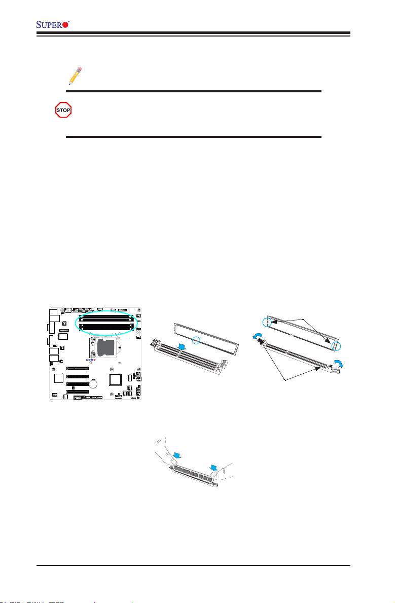
2-3 Installing DDR3 Memory ............................................................................... 2-10
DIMM Installation .......................................................................................... 2-10
Removing Memory Modules ......................................................................... 2-10
Memory Support .............................................................................................2-11
Memory Population Guidelines ......................................................................2-11
2-4 Motherboard Installation ................................................................................ 2-13
Tools Needed ................................................................................................ 2-13
Location of Mounting Holes .......................................................................... 2-13
Installing the Motherboard ............................................................................ 2-14
2-5 Connectors/IO Ports ...................................................................................... 2-15
Back I/O Panel .............................................................................................. 2-15
ATX PS/2 Keyboard/Mouse Ports ............................................................ 2-16
Universal Serial Bus (USB) ...................................................................... 2-17
Ethernet Ports .......................................................................................... 2-18
Serial Ports ............................................................................................... 2-19
Video Connector ....................................................................................... 2-20
Page 7

vii
Table of Contents
Front Control Panel ....................................................................................... 2-21
FrontControlPanelPinDenitions............................................................... 2-22
Power LED .............................................................................................. 2-22
HDD LED .................................................................................................. 2-22
NIC1/NIC2 (LAN1/LAN2) .......................................................................... 2-23
Overheat (OH)/Fan Fail/Front UID LED ................................................... 2-23
Reset Button ........................................................................................... 2-24
Power Button ........................................................................................... 2-24
2-6 Connecting Cables ........................................................................................ 2-25
ATX Main PWR & CPU PWR Connectors .............................................. 2-25
Fan Headers ............................................................................................. 2-26
Chassis Intrusion ..................................................................................... 2-26
Internal Buzzer ......................................................................................... 2-27
Speaker .................................................................................................... 2-27
Onboard Power LED ................................................................................ 2-28
Power Supply I
2
C Connector.................................................................... 2-28
T-SGPIO 0/1 Headers .............................................................................. 2-29
TPM Header ............................................................................................. 2-29
DOM PWR Connector .............................................................................. 2-30
Wake-On-LAN .......................................................................................... 2-30
2-7 Jumper Settings ............................................................................................ 2-31
Explanation of Jumpers ................................................................................ 2-31
LAN Port Enable/Disable ......................................................................... 2-31
CMOS Clear ............................................................................................. 2-32
PCI Slot SMB Enable ............................................................................... 2-32
VGA Enable .............................................................................................. 2-33
Watch Dog Enable ................................................................................... 2-33
USB Wake-Up ......................................................................................... 2-34
BMC Enable ............................................................................................. 2-34
ME Recovery ............................................................................................ 2-35
2-8 Onboard Indicators ........................................................................................ 2-36
LAN 1/LAN 2 LEDs .................................................................................. 2-36
IPMI Dedicated LAN LEDs ..................................................................... 2-36
IPMI Heartbeat LED ................................................................................. 2-37
Power Standby LED ................................................................................. 2-37
2-9 SATA Connections ......................................................................................... 2-38
SATA Connections .................................................................................... 2-38
Page 8

viii
X9SCM/X9SCM-F/X9SCL/X9SCL-F/X9SCL+-F User’s Manual
Chapter 3 Troubleshooting
3-1 Troubleshooting Procedures ........................................................................... 3-1
3-2 Technical Support Procedures ........................................................................ 3-3
3-3 Frequently Asked Questions ........................................................................... 3-4
3-4 Battery Removal and Installation .................................................................... 3-6
3-5 Returning Merchandise for Service................................................................. 3-7
Chapter 4 BIOS
4-1 Introduction ...................................................................................................... 4-1
4-2 Main Setup ...................................................................................................... 4-2
4-3 AdvancedSetupCongurations...................................................................... 4-4
4-4 Event Logs .................................................................................................... 4-15
4-5 IPMIConguration(X9SCM-F/X9SCL-F/X9SCL+-F) .................................... 4-16
4-6 Boot Settings ................................................................................................ 4-18
4-7 Security Settings ........................................................................................... 4-19
4-8 Exit Options ................................................................................................... 4-20
Appendix A BIOS Error Beep Codes
A-1 BIOS Error Beep Codes .................................................................................A-1
Appendix B Software Installation Instructions
B-1 Installing Drivers ..............................................................................................B-1
B-2 ConguringSuperDoctor
®
III ..........................................................................B-2
Appendix C UEFI BIOS Recovery Instructions
An Overview to the UEFI BIOS ..................................................................................... 1
How to Recover the UEFI BIOS Image (-the Main BIOS Block) .................................. 1
To Recover the Main BIOS Block Using a USB-Attached Device ................................ 1
Page 9

Chapter 1: Introduction
1-1
Chapter 1
Introduction
1-1 Overview
Checklist
Congratulations on purchasing your computer motherboard from an acknowledged
leader in the industry. Supermicro boards are designed with the utmost attention to
detail to provide you with the highest standards in quality and performance.
Please check that the following items have all been included with your motherboard.
If anything listed here is damaged or missing, contact your retailer.
The following items are included in the retail box:
•One (1) Supermicro Mainboard
•Six (6) SATA cables
•One (1) I/O shield
•One (1) Supermicro CD containing drivers and utilities
•One (1) User's Manual
Page 10
1-2
X9SCM/X9SCM-F/X9SCL/X9SCL-F/X9SCL+-F User’s Manual
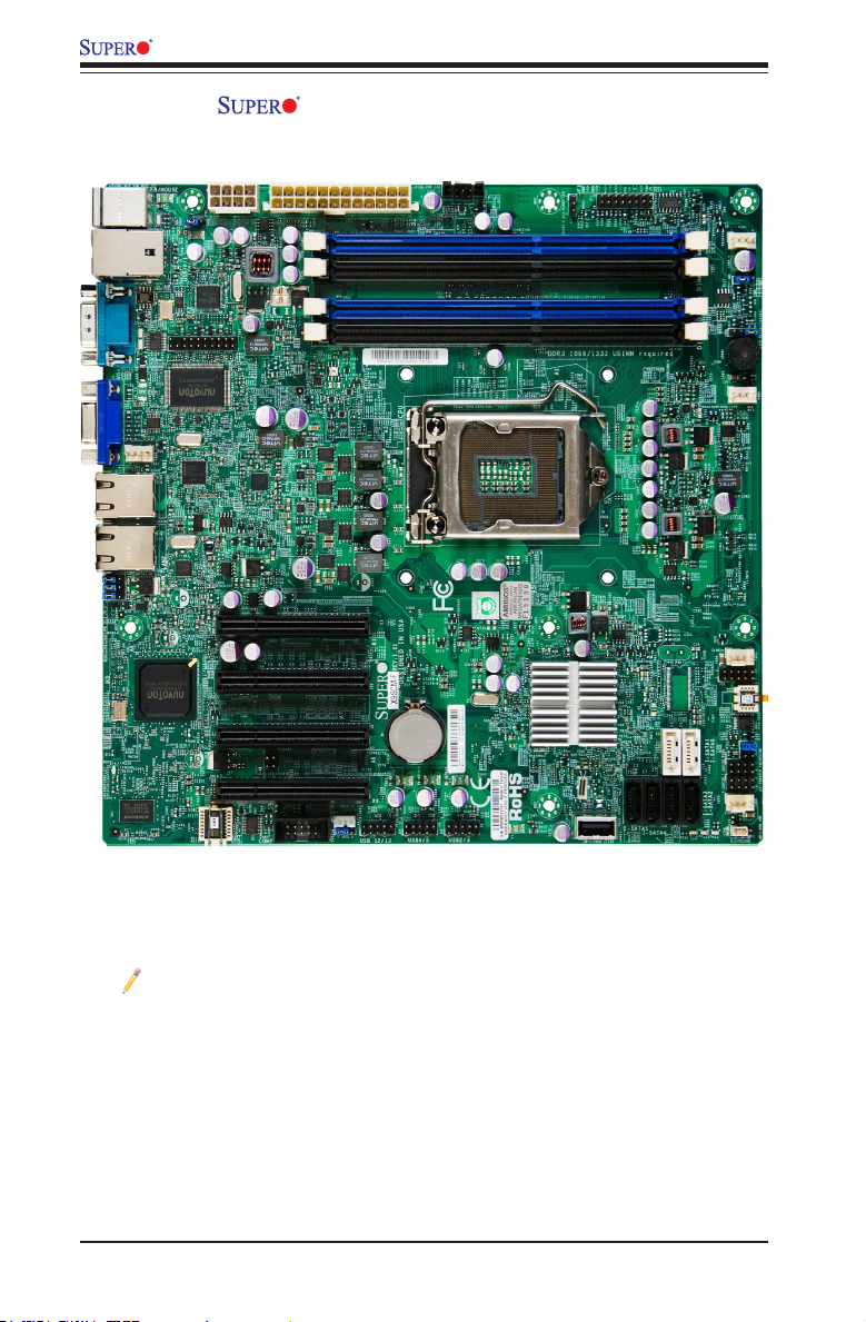
Motherboard Image (X9SCM/X9SCM-F)
Note: All graphics shown in this manual were based upon the latest PCB
Revision available at the time of publishing of the manual. The motherboard
you've received may or may not look exactly the same as the graphics
shown in this manual.
Page 11
Chapter 1: Introduction
1-3
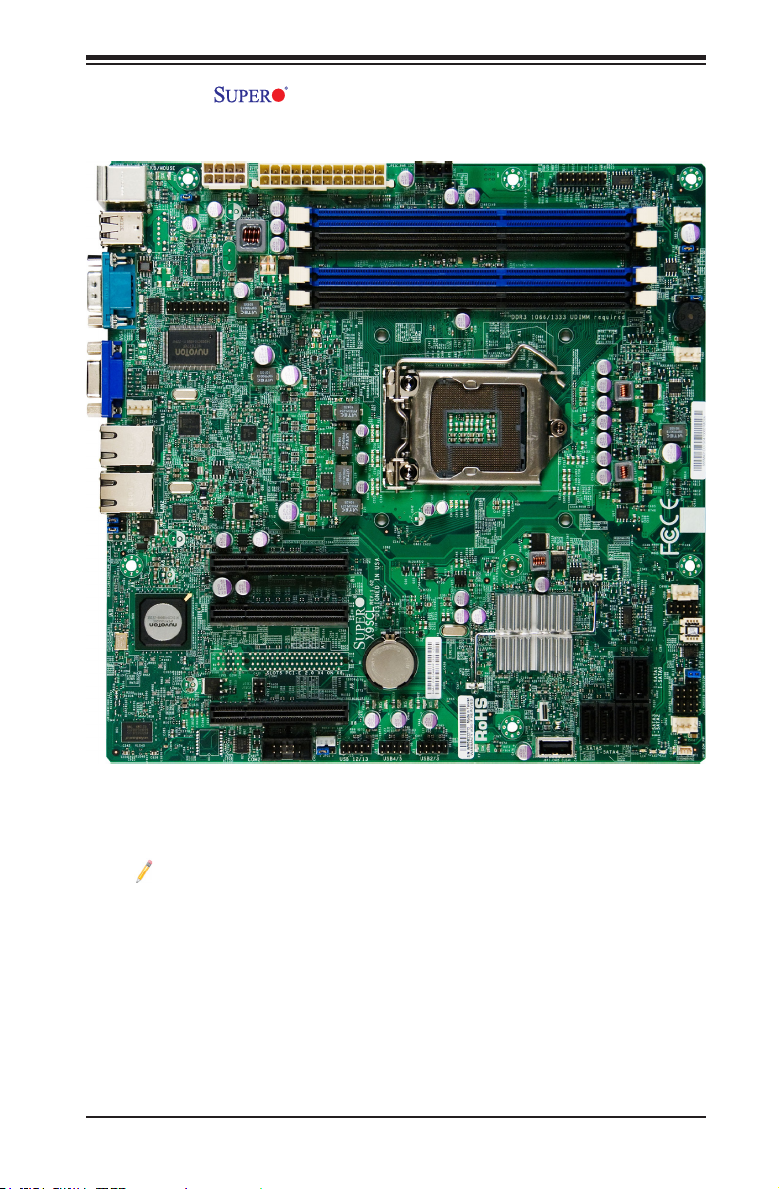
Motherboard Image (X9SCL/X9SCL-F)
Note: All graphics shown in this manual were based upon the latest PCB
Revision available at the time of publishing of the manual. The motherboard
you've received may or may not look exactly the same as the graphics
shown in this manual.
Page 12
1-4
X9SCM/X9SCM-F/X9SCL/X9SCL-F/X9SCL+-F User’s Manual
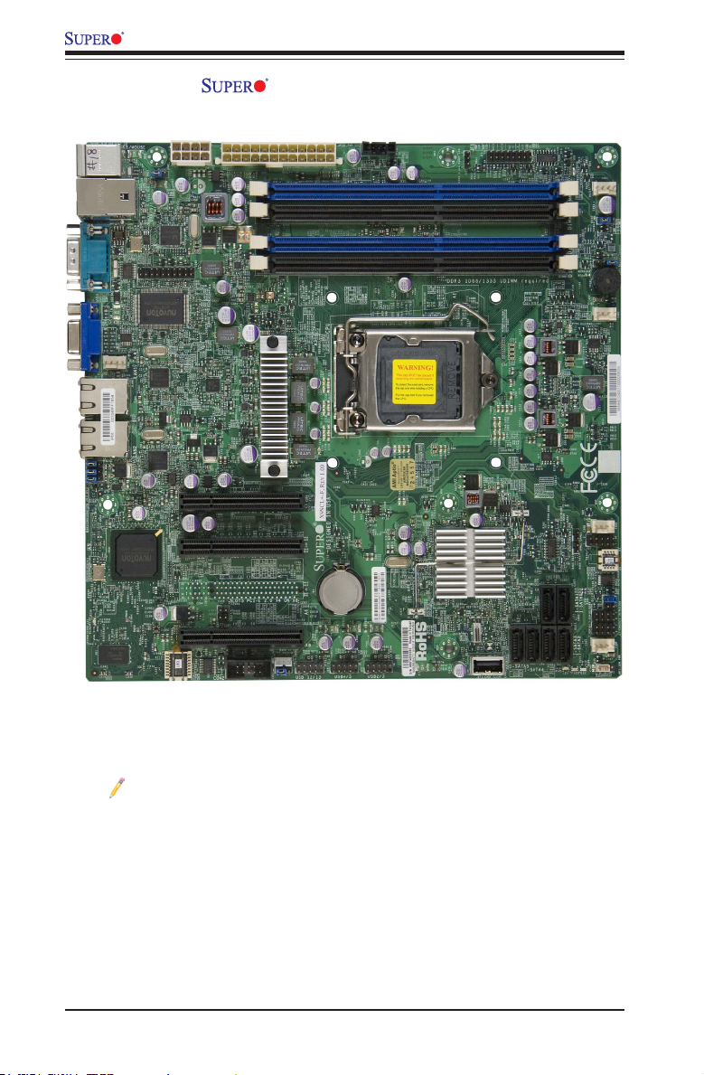
Motherboard Image (X9SCL+-F)
Note: All graphics shown in this manual were based upon the latest PCB
Revision available at the time of publishing of the manual. The motherboard
you've received may or may not look exactly the same as the graphics
shown in this manual.
Page 13
Chapter 1: Introduction
1-5
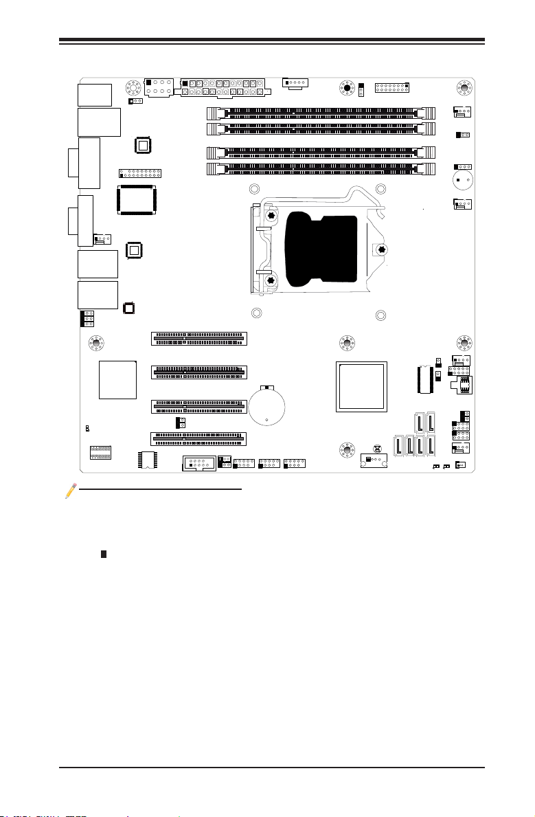
Motherboard Layout
Important Notes to the User
•See Chapter 2 for detailed information on jumpers, I/O ports and JF1 front
panel connections.
•" " indicates the location of "Pin 1".
•Jumpers not indicated are for testing only.
•SATA-III ports (6Gb/s) are available on the X9SCM(-F) only.
•For X9SCM(-F): Two SATA-III ports (I-SATA#0~1) and four SATA-II ports (3
Gb/s, I-SATA#2~5) are located on the board. For X9SCL(+)(-F): Six SATA-II
ports (I-SATA #0~5) are included on the motherboard.
•PCI-E Slot5 (PCI-E 2.0 x4 on x8 slot) is available on the X9SCM(-F) only.
J31
JTPM
J29
JL1
JI2C2
JI2C1
T-SGPIO1
JWF1
JPW2
JWOL
JSPK
JPI2C
JPW1
COM1
SPKR1
JBT1
LE2
JWD
JLED1
JPL2
JPG1
JPB
JPL1
JPUSB1
FAN1
FANA
FAN3
FAN2
USB4/5
USB 12/13
_LAN
IPMI
COM2
VGA
USB11
DIMM2B
DIMM2A
USB2/3
Slot6 PCI-E 3.0/2.0 x8
JF1
I-SATA2
Slot4 PCI-E 2.0 x4 on x8
KB/MOUSE
DIMM1B
DIMM1A
CPU
Slot7 PCI-E 3.0/2.0 x8
BIOS
B1
Battery
LAN
BMC
CTRL
S I/O
T-SGPIO2
FP CTRL
Cougar Point
Standard PCH
Memory Chip
Fan4
LAN
(*I-SATA 0/1: SATA3)
I-SATA4
I-SATA5
I-SATA3
I-SATA1
I-SATA0
Slot5 PCI-E 2.0 x4 on x8
USB/0/1
LAN1
LAN2
LE7
JPME1
JPME2
LE4
LAN
Page 14
1-6
X9SCM/X9SCM-F/X9SCL/X9SCL-F/X9SCL+-F User’s Manual
J31
JTPM
J29
JL1
JI2C2
JI2C1
T-SGPIO1
JWF1
JPW2
JWOL
JSPK
JPI2C
JPW1
COM1
SPKR1
JBT1
LE2
JWD
JLED1
JPL2
JPG1
JPB
JPL1
JPUSB1
FAN1
FANA
FAN3
FAN2
USB4/5
USB 12/13
_LAN
IPMI
COM2
VGA
USB11
DIMM2B
DIMM2A
USB2/3
Slot6 PCI-E 3.0/2.0 x8
JF1
I-SATA2
Slot4 PCI-E 2.0 x4 on x8
KB/MOUSE
DIMM1B
DIMM1A
CPU
Slot7 PCI-E 3.0/2.0 x8
BIOS
B1
Battery
LAN
BMC
CTRL
S I/O
T-SGPIO2
FP CTRL
Cougar Point
Standard PCH
Memory Chip
Fan4
LAN
(*I-SATA 0/1: SATA3)
I-SATA4
I-SATA5
I-SATA3
I-SATA1
I-SATA0
Slot5 PCI-E 2.0 x4 on x8
USB/0/1
LAN1
LAN2
LE7
JPME1
JPME2
LE4
LAN
1
4
1
1
X9SCM/X9SCM-F/X9SCL/X9SCL-F/X9SCL+-F Jumpers
Number Jumper Description Default
34 J29 SPI Programming (internal use) Closed (Normal)
22 JBT1 CMOS Clear (See Chpt. 2)
13 JI
2
C1/JI
2
C2 SMB to PCI Slots (See Chpt. 2)
12 JPB BMC Enable Pins 1-2 (Enabled)
17 JPG1 Onboard VGA Enable Pins 1-2 (Enabled)
10,11 JPL1/JPL2 LAN1/LAN2 Enable Pins 1-2 (Enabled)
48 JPUSB1 USB 0/1 Wake-Up Enable Pins 1-2 (Enabled)
41 JWD Watch_Dog Timer Enable Pins 1-2 (Reset)
51 JPME1 ME Recovery Open (Normal)
1
2
1
3
1
5
1
7
1
8
1
10
1
13
1
14
1
15
1
22
1
21
1
25
1
31
1
33
1
34
1
35
1
36
1
38
1
6
1
11
1
39
1
40
1
41
1
42
1
43
1
9
1
12
1
44
1
45
1
46
1
47
1
48
X9SCM/X9SCM-F/X9SCL/X9SCL-F/X9SCL+-F Quick Reference
1
16
1
17
1
18
1
19
1
20
1
23
1
24
1
26
1
27
1
32
1
37
1
30
1
29
1
50
1
51
1
49
1
52
Page 15
Chapter 1: Introduction
1-7
X9SCM/X9SCM-F/X9SCL/X9SCL-F/X9SCL+-F LED Indicators
Number LED Description Color/State Status
14 LE7 IPMI Heartbeat LED Green: Blinking IPMI Active
52 LE4 Power Standby Green: Solid on System is plugged in
X9SCM/X9SCM-F/X9SCL/X9SCL-F/X9SCL+-F Headers/Connectors
Number Connector Description
21 B1 Onboard Battery
4,16 COM1/COM2 COM1/2 Serial Connection Headers
35 BIOS SPI BIOS
42,38,37,7,30 Fans 1~4, Fan A System/CPU Fan Headers
36 J31 SPI Programming (internal use)
43 JF1 Front Panel Control Header
33 JL1 Chassis Intrusion Header
44 JLED1 Power LED Indicator Header
46 JPW1 24-pin ATX Main Power Connector (Required)
47 JPW2 +12V 8-pin CPU power Connector (Required)
1 KB/Mouse Keyboard/Mouse Connectors
8,9,3 LAN1/LAN2, IPMI_LAN Gigabit (RJ45) Ports (LAN1/2), IPMI_LAN (F-models)
50,49 I-SATA 0/1 Serial ATA Ports 0/1 (X9SCL: SATA-II Ports, X9SCM:
SATA-III Ports)
27,26,25,24 I-SATA 2~5 SATA-II Ports
45 JPI
2
C PWR supply (I
2
C) System Management Bus
40 JSPK Speaker Header (Pins 3/4: Internal, 1~4:External)
5 JTPM Trusted Platform Module (TPM) Header
29 JWF1 SATA DOM (Device_On_Module) Power Connector
15 JWOL Wake_On_LAN Header
39 SPKR1 Internal Speaker/Buzzer
31, 32 T-SGPIO-1/2 Serial_Link General Purpose IO 1/2 Headers (5V
Gen1/Gen 2)
2 USB0/1 Backpanel USB 0/1
20,19,18 USB2/3, USB4/5,
USB 12/13
Front Accessible USB Connections (via 3 Headers)
23 USB 11 Front Accessible Type A USB Connector
6 VGA Onboard Video Port
Page 16
1-8
X9SCM/X9SCM-F/X9SCL/X9SCL-F/X9SCL+-F User’s Manual
Motherboard Features
CPU Single Intel® Xeon E3-1200 & E3-1200 v2 series, 2nd
& 3rd generation Intel Core® i3, Pentium®, Celeron®
processor in an LGA 1155 socket.
Memory Four (4) SDRAM DIMM slots support up to 32 GB of
DDR3 Unbuffered, ECC 1600/1333/1066 MHz memory.
Note: For memory speed 1600 MHz support, an E3-
1200 v2 CPU is required.
Supports dual-channel memory bus
DIMM sizes
UDIMM 1 GB, 2 GB, 4GB and 8GB
Chipset Intel® C204 Express (X9SCM Series)
Intel® C202 Express (X9SCL Series)
Expansion Slots Two (2) PCI Express 2.0 x8 slots
Two (2) PCI Express x4 in x8 slots, One (1) on the
X9SCL/X9SCL-F/X9SCL+-F
Integrated Graphics Matrox® G200eW
Network Connections One (1) Intel 82574L Gigabit Ethernet controller for
LAN 1, and one (1) Intel 82579 PHY for LAN 2. Note:
The X9SCL+-F features two (2) Intel 82574L Gigabit
Ethernet controllers, one each for LAN 1 and LAN 2.
Two (2) RJ-45 Rear IO Panel Connectors with Link
and Activity LEDs
Single Realtek RTL8201N PHY to support IPMI 2.0
LAN (X9SCM-F/X9SCL-F/X9SCL+-F Only)
I/O Devices SATA Connections
(X9SCM/X9SCM-F)
•SATA-III Ports (6Gb/s) •Two (2) (I-SATA 0/1)
•SATA-II Ports (3Gb/s) •Four (4) (I-SATA 2~5)
(X9SCL/X9SCL-F/X9SCL+-F)
•SATA-II Ports •Six (6) (I-SATA 0~5)
RAID (Windows) RAID 0, 1, 5, 10
Onboard IPMI (X9SCM-F/X9SCL-F/X9SCL+-F Only)
IPMI 2.0 supported by the WPCM450 Server BMC
USB Devices
Two (2) USB ports on the rear IO panel (USB 0/1)
Six (6) USB header connectors for front access (USB
2/3, USB 4/5, USB 12/13)
One (1) Type A USB internal connector (USB 11)
Page 17
Chapter 1: Introduction
1-9
Keyboard/Mouse
PS/2 Keyboard/Mouse ports on the I/O backpanel
Serial (COM) Ports
Two (2) Fast UART 16550 connections: one 9-pin
RS-232 port (Backplane COM1 port) and one header
(FP COM2)
Super I/O
Winbond Super I/O NCP6776F
BIOS 64 MB SPI AMI BIOS
®
SM Flash BIOS
Play and Plug (PnP0, DMI 2.3, PCI 2.3, ACPI
1.0/2.0/3.0, USB Keyboard and SMBIOS 2.5
Power Conguration ACPI/ACPM Power Management
Main Switch Override Mechanism
Keyboard Wake-up from Soft-Off
Internal/External Modem Ring-On
Power-on mode for AC power recovery
PC Health Monitoring CPU Monitoring
Onboard voltage monitors for CPU core, +3.3V, +5V,
+/-12V, +3.3V Stdby, VBAT, Memory, VCORE for CPU
CPU 4-phase switching voltage regulator
CPU/System overheat LED and control
CPU Thermal Trip support
Thermal Monitor 2 (TM2) support
Fan Control
Fan status monitoring with rmware 4-pin (Pulse Width
Modulation) fan speed control
Low noise fan speed control
System Management PECI (Platform Environment Conguration Interface)
3.0 support
System resource alert via SuperDoctor® III
SuperDoctor® III, Watch Dog, NMI
Chassis Intrusion header and detection
CD Utilities BIOS ash upgrade utility
Drivers and software for Intel® Cougar Point chipset
utilities
Other ROHS 6/6 (Full Compliance, Lead Free)
Dimensions Micro ATX form factor (9.6" x 9.6") (243.84mm x
243.84mm)
Page 18

1-10
X9SCM/X9SCM-F/X9SCL/X9SCL-F/X9SCL+-F User’s Manual
Note: For IPMI Conguration Instructions, please refer to the Embedded
IPMI Conguration User's Guide available @ http://www.supermicro.com/
support/manuals/.
Page 19
Chapter 1: Introduction
1-11
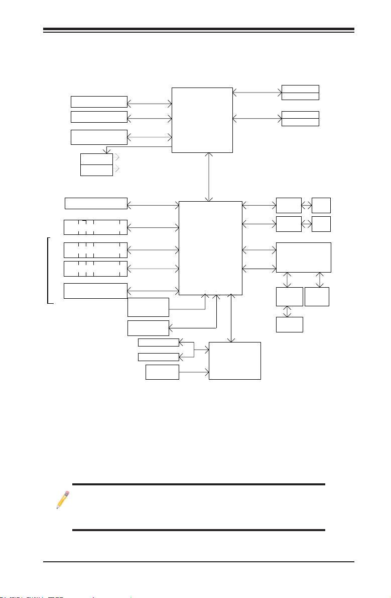
System Block Diagram
Note: This is a general block diagram and may not exactly represent
the features on your motherboard. See the Motherboard Features
pages for the actual specications of each motherboard.
Cougar Point
DDR3 (CHA)
LGA 1155 Socket
CPU
PCIe2.0_x8
VRM 12
SVID
LPC I/O
NCT6776F
PCIe x8 Slot
RJ45
RJ45
DDR3 (CHB)
DIMM1
DIMM2(Far)
DIMM1
DIMM2(Far)
4 UDIMM
MISC VRs
1333/1066MHz
1333/1066MHz
5.0Gb
x4 DMI II
5.0Gb
5.0Gbps
PCIe_x4
PCIe x8 Slot
6/4 SATA Ports
SATA-II
300MB/s
9 USB Ports
USB2.0
480Mbps
Flash
SPI 32Mb
SPI
PCIe_x1
2.5Gbps
GLAN1
82574L
(Reserved)
COM1,2
P/S2
LPC
HEALTH
INFO
LPC
TPM1.2 Header
LPC
PCIe_x1
2.5Gbps
GLAN2
82579*
RMII
VGA
Port
RTL8201
PHY
Hermon WPCM450
Winbond BMC
PCI32
RJ45
PCIe2.0_x8
PCIe x8 Slot
5.0Gb
PCIe2.0_x4
5.0Gb
PCIe x8 Slot
600MB/s
SATA-III
0/2 SATA Ports
PCH
(X9SCM seires only)
(X9SCL/X9SCM)
(*See Note below)
(*Note:
6 SATA-II ports for X9SCL,
4 SATA-II & 2 SATA-III ports
for X9SCM)
(Slot 5)
(Slot 7)
(Slot 6)
(Slot 4)
*82574L for the X9SCL+-F
X9SCM/X9SCM-F/X9SCL/X9SCL-F/X9SCL+-F Block Diagram
Page 20

1-12
X9SCM/X9SCM-F/X9SCL/X9SCL-F/X9SCL+-F User’s Manual
1-2 Chipset Overview
The X9SCM/X9SCM-F/X9SCL/X9SCL-F/X9SCL+-F supports a single Intel® Xeon
E3-1200 series, 2nd generation Intel Core® i3, Pentium®, Celeron® processor in
an LGA 1155 socket. Built upon the functionality and the capability of the Intel
C202/C204 chipset, the motherboard provides substantial enhancement to system
performance and storage capability for entry-level to mid-range servers in a sleek
package.
The high-speed Direct Media Interface (DMI) featured in the Intel C202/C204
chipset supports high-speed Direct Media Interface (DMI) for chip-to-chip true iso-
chronous communication, providing up to 10 Gb/s of sof tware-transparent data
transfer rate on each read/write direction. In addition, the X9SCM/X9SCM-F/
X9SCL/X9SCL-F/X9SCL+-F also features a TCO timer which allows the system
to recover from a software/hardware lock and perform tasks, including ECC Error
Reporting, Function Disable and Intruder Detect.
Intel C202/C204 Express Chipset Features
•Direct Media Interface (up 20 Gb/s transfer, Full Duplex)
•Intel® Intel Rapid Storage Technology
•Intel I/O Virtualization (VT-d) Support
•Intel Trusted Execution Technology Support
•PCI Express 2.0 Interface (up to 5.0 GT/s)
•SATA Controller
•6G/s on up to two ports
•3G/s on all ports
•Advanced Host Controller Interface (AHCI)
Page 21

Chapter 1: Introduction
1-13
1-3 Special Features
Recovery from AC Power Loss
Basic I/O System (BIOS) provides a setting for you to determine how the system
will respond when AC power is lost and then restored to the system. You can
choose for the system to remain powered off (in which case you must press the
power switch to turn it back on), or for it to automatically return to a power-on state.
See the Advanced BIOS Setup section to change this setting. The default setting
is Last State.
1-4 PC Health Monitoring
This section describes the PC health monitoring features of the board. All have
an onboard System Hardware Monitoring chip that supports PC health monitoring.
An onboard voltage monitor will scan these onboard voltages continuously: CPU
Vcore, NIC Vcore, BMC Vcore, AUX Vcore, Standby ME Vcore, 12V Scale, 1.5V,
3.3V Vcc(V), 3.3VSB, and Battery Voltage. Once a voltage becomes unstable, a
warning is given, or an error message is sent to the screen. The user can adjust
the voltage thresholds to dene the sensitivity of the voltage monitor.
Fan Status Monitor with Firmware Control
PC health monitoring in the BIOS can check the RPM status of the cooling fans. The
onboard CPU and chassis fans are controlled by Thermal Management via BIOS
(under the Hardware Monitoring section in the Advanced Setting).
Environmental Temperature Control
The thermal control sensor monitors the CPU temperature in real time and will turn
on the thermal control fan whenever the CPU temperature exceeds a user-dened
threshold. The overheat circuitry runs independently from the CPU. Once the ther-
mal sensor detects that the CPU temperature is too high, it will automatically turn
on the thermal fans to prevent the CPU from overheating. The onboard chassis
thermal circuitry can monitor the overall system temperature and alert the user when
the chassis temperature is too high.
Note: To avoid possible system overheating, please be sure to provide
adequate airow to your system.
System Resource Alert
This feature is available when the system is used with SuperDoctor® III in the
Page 22

1-14
X9SCM/X9SCM-F/X9SCL/X9SCL-F/X9SCL+-F User’s Manual
Windows OS environment or used with SuperDoctor II in Linux. SuperDoctor
is used to notify the user of certain system events. For example, you can also
congure SuperDoctor to provide you with warnings when the system temperature,
CPU temperatures, voltages and fan speeds go beyond predened thresholds.
1-5 ACPI Features
ACPI stands for Advanced Conguration and Power Interface. The ACPI specica-
tion denes a exible and abstract hardware interface that provides a standard
way to integrate power management features throughout a PC system, including
its hardware, operating system and application software. This enables the system
to automatically turn on and off peripherals such as CD-ROMs, network cards, hard
disk drives and printers.
In addition to enabling operating system-directed power management, ACPI also
provides a generic system event mechanism for Plug and Play, and an operating
system-independent interface for conguration control. ACPI leverages the Plug and
Play BIOS data structures, while providing a processor architecture-independent
implementation that is compatible with Windows XP, Windows Vista and Windows
2008 Operating Systems.
Slow Blinking LED for Suspend-State Indicator
When the CPU goes into a suspend state, the chassis power LED will start to blink
to indicate that the CPU is in suspend mode. When the user presses any key, the
CPU will "wake up", and the LED will automatically stop blinking and remain on.
1-6 Power Supply
As with all computer products, a stable power source is necessary for proper and
reliable operation. It is even more important for processors that have high CPU
clock rates.
This motherboard accommodates 24-pin ATX power supplies. Although most
power supplies generally meet the specications required by the CPU, some are
inadequate. In addition, the 12V 8-pin power connector located at JPW2 is also
required to ensure adequate power supply to the system. Also your power supply
must supply 1.5A for the Ethernet ports.
Warning: Please use a power supply that contains a 24-pin and an 8-pin or a 4-pin
power connector. Be sure to connect these connectors to the 24-pin (JPW1) and the
8-pin (JPW2) power connectors on the motherboard.
Note: The JPW2 power connector on the motherboard also supports
one 4-pin connector.
Page 23

Chapter 1: Introduction
1-15
It is strongly recommended that you use a high quality power supply that meets ATX
power supply Specication 2.02 or above. It must also be SSI compliant. (For more
information, please refer to the web site at http://www.ssiforum.org/). Additionally, in
areas where noisy power transmission is present, you may choose to install a line
lter to shield the computer from noise. It is recommended that you also install a
power surge protector to help avoid problems caused by power surges.
1-7 Super I/O
The Super I/O supports two high-speed, 16550 compatible serial communication
ports (UARTs). Each UART includes a 16-byte send/receive FIFO, a programmable
baud rate generator, complete modem control capability and a processor interrupt
system. Both UARTs provide legacy speed with baud rate of up to 115.2 Kbps
as well as an advanced speed with baud rates of 250 K, 500 K, or 1 Mb/s, which
support higher speed modems.
The Super I/O provides functions that comply with ACPI (Advanced Conguration
and Power Interface), which includes support of legacy and ACPI power manage-
ment through an SMI or SCI function pin. It also features auto power management
to reduce power consumption.
1-8 Overview of the Nuvoton WPCM450 Controller
The Nuvoton WPCM450R Controller is a Baseboard Management Controller (BMC)
that supports 2D/VGA-compatible Graphics cores, Virtual Media, and Keyboard/
Video/Mouse Redirection (KVMR) modules. With blade-oriented Super I/O capability
built in, the WPCM450R Controller is ideal for legacy-reduced server platforms.
The WPCM450R interfaces with a host system via PCI interface to communicate
with the Graphics core. It supports USB 2.0 and 1.1 for remote keyboard/mouse/
virtual media emulation. It also provides LPC interface to control Super IO func-
tions. The WPCM450R is connected to the network via an external Ethernet PHY
module.
The WPCM450R communicates with onboard components via six SMBus inter-
faces, fan control, and Platform Environment Control Interface (PECI) buses.
Note: For more information on IPMI conguration, please refer to the
Embedded IPMI User's Guide posted on our Website @ http://www.su-
permicro.com/support/manuals/.
Page 24

1-16
X9SCM/X9SCM-F/X9SCL/X9SCL-F/X9SCL+-F User’s Manual
Notes
Page 25

Chapter 2: Installation
2-1
Chapter 2
Installation
2-1 Static-Sensitive Devices
Electrostatic-Discharge (ESD) can damage electronic com ponents. To avoid dam-
aging your system board, it is important to handle it very carefully. The following
measures are generally sufcient to protect your equipment from ESD.
Precautions
• Use a grounded wrist strap designed to prevent static discharge.
• Touch a grounded metal object before removing the board from the antistatic
bag.
• Handle the board by its edges only; do not touch its components, peripheral
chips, memory modules or gold contacts.
• When handling chips or modules, avoid touching their pins.
• Put the motherboard and peripherals back into their antistatic bags when not in
use.
• For grounding purposes, make sure your computer chassis provides excellent
conductivity between the power supply, the case, the mounting fasteners and
the motherboard.
• Use only the correct type of onboard CMOS battery. Do not install the onboard
battery upside down to avoid possible explosion.
Unpacking
The motherboard is shipped in antistatic packaging to avoid static damage. When
unpacking the board, make sure that the person handling it is static protected.
Page 26
2-2
X9SCM/X9SCM-F/X9SCL/X9SCL-F/X9SCL+-F User’s Manual
2-2 Processor and Heatsink Installation
Warning: When handling the processor package, avoid placing direct pressure on the
label area of the fan.
Notes:
•Always connect the power cord last, and always remove it before adding,
removing or changing any hardware components. Make sure that you install
the processor into the CPU socket before you install the CPU heatsink.
•If you buy a CPU separately, make sure that you use an Intel-certied multi-
directional heatsink only.
•Make sure to install the system board into the chassis before you install
the CPU heatsink.
•When receiving a server board without a processor pre-installed, make sure
that the plastic CPU socket cap is in place and none of the socket pins are
bent; otherwise, contact your retailer immediately.
•Refer to the Supermicro website for updates on CPU support.
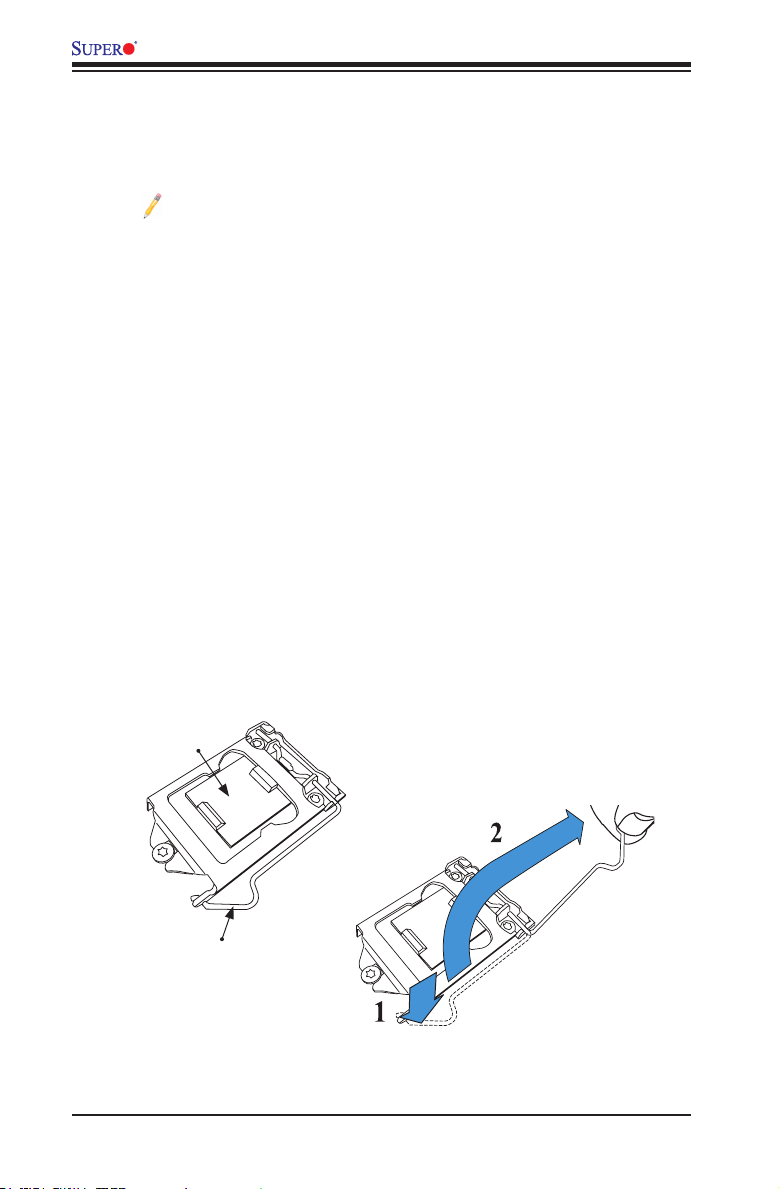
Load Lever
Installing the LGA1155 Processor
1. Press the load lever to release the load plate, which covers the CPU socket,
from its locking position.
Load Plate
Page 27
Chapter 2: Installation
2-3
2. Gently lift the load lever to open the load plate. Remove the plastic cap.
3. Use your thumb and your index nger to hold the CPU at the North center
edge and the South center edge of the CPU.
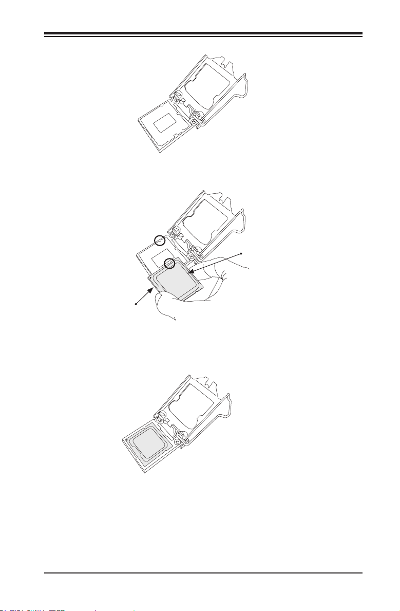
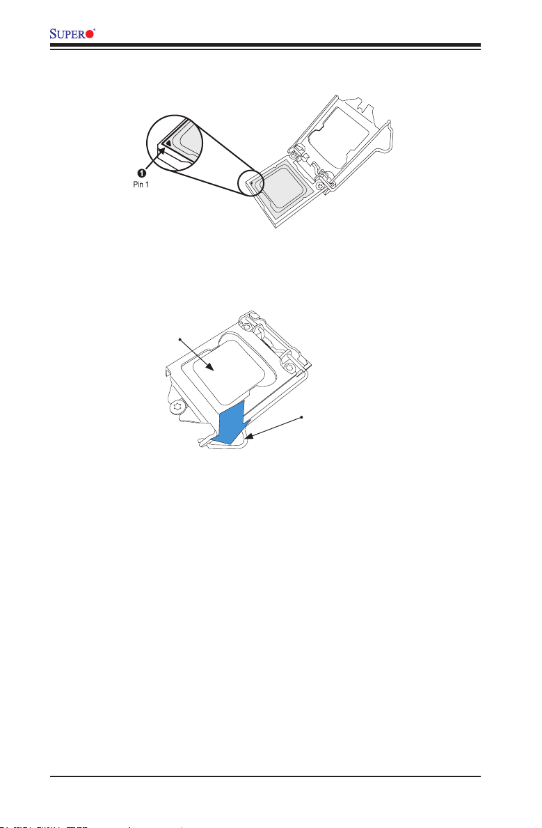
4. Align the CPU key that is the semi-circle cutouts against the socket keys.
Once it is aligned, carefully lower the CPU straight down into the socket. (Do
not drop the CPU on the socket. Do not move the CPU horizontally or verti-
cally.
South Center Edge
North Center Edge
Page 28
2-4
X9SCM/X9SCM-F/X9SCL/X9SCL-F/X9SCL+-F User’s Manual
Warning: You can only install the CPU inside the socket only in one direction. Make
sure that it is properly inserted into the CPU socket before closing the load plate. If it
doesn't close properly, do not force it as it may damage your CPU. Instead, open the
load plate again and double-check that the CPU is aligned properly.
CPU properly
installed
Load lever locked
into place
5. Do not rub the CPU against the surface or against any pins of the socket to
avoid damaging the CPU or the socket.)
6. With the CPU inside the socket, inspect the four corners of the CPU to make
sure that the CPU is properly installed.
7. Use your thumb to gently push the load lever down to the lever lock.
Page 29
Chapter 2: Installation
2-5
Mounting Holes
Motherboard
Screw#1
Screw#2
Heatsink Bracket
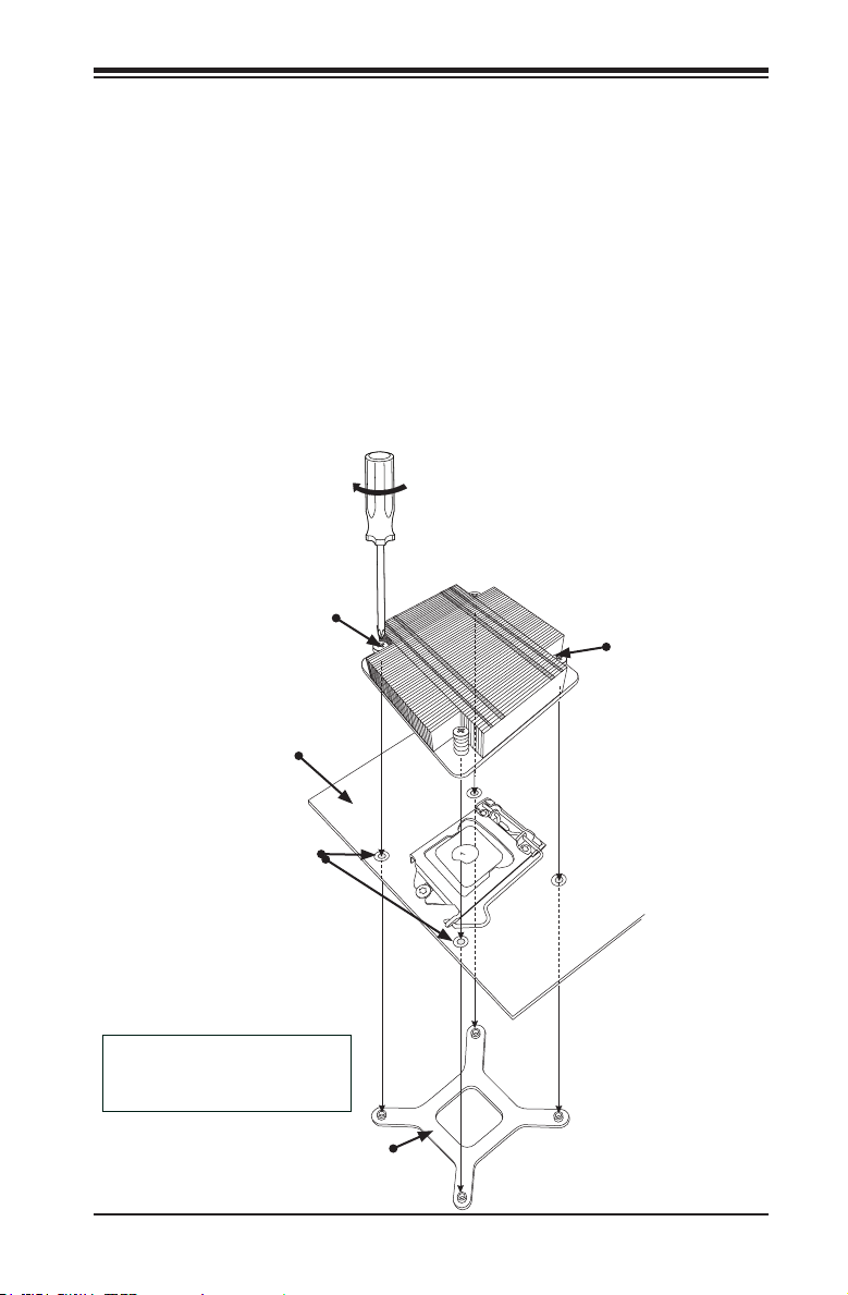
Installing a Passive CPU Heatsink
1. Do not apply any thermal grease to the heatsink or the CPU die -- the re-
quired amount has already been applied.
2. Place the heatsink on top of the CPU so that the four mounting holes are
aligned with those on the Motherboard's and the Heatsink Bracket under-
neath.
3. Screw in two diagonal screws (i.e., the #1 and the #2 screws) until just snug
(-do not over-tighten the screws to avoid possible damage to the CPU.)
4. Finish the installation by fully tightening all four screws.
Recommended Supermicro
heatsink:
SNK-P0046P heatsink with BKT-
0028L bottom bracket
Page 30
2-6
X9SCM/X9SCM-F/X9SCL/X9SCL-F/X9SCL+-F User’s Manual
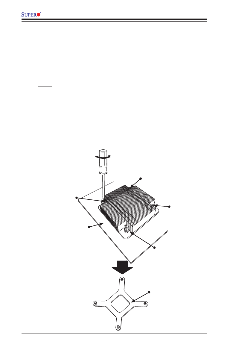
Removing the Heatsink
Warning: We do not recommend that the CPU or the heatsink be removed. However,
if you do need to uninstall the heatsink, please follow the instructions below to uninstall
the heatsink to prevent damage done to the CPU or the CPU socket.
1. Unscrew the heatsink screws from the motherboard in the sequence as
shown in the illustration below.
2. Gently wriggle the heatsink to loosen it from the CPU. (Do not use excessive
force when wriggling the heatsink!!)
3. Remove the heatsink, then remove the CPU from the CPU socket.
4. Clean the surface of the CPU and the heatsink, removing the used thermal
grease. Reapply the proper amount of thermal grease on the surface before
re-installing the CPU and the heatsink.
Loosen screws in
sequence as shown.
Screw#2
Motherboard
Remove the Heatsink
Bracket from underneath
the motherboard.
Screw#1
Screw#3
Screw#4
Page 31

Chapter 2: Installation
2-7
Thermal Grease
Heatsink
Fins
Recommended Supermicro
heatsink:
SNK-P0046A4 active heatsink
Installing an Active Fan
CPU Heatsink
1. Locate the CPU Fan power connec-
tor on the motherboard. (Refer to
the layout on the right for the CPU
Fan location.)
2. Position the heatsink so that the
heatsink fan wires are closest to the
CPU fan power connector and are
not interfered with other compo-
nents.
3. Inspect the CPU Fan wires to make
sure that the wires are routed
through the bottom of the heatsink.
4. Remove the thin layer of the protec-
tive lm from the copper core of the
heatsink.
Warning: CPU may overheat if the protec-
tive lm is not removed from the heatsink.
5. Apply the proper amount of thermal
grease on the CPU.
Note: If your heatsink came with
a thermal pad, please ignore
this step.
6. If necessary, rearrange the wires
to make sure that the wires are not
pinched between the heatsink and
the CPU. Also make sure to keep
clearance between the fan wires
and the ns of the heatsink.
7. Align the four heatsink fasteners
with the mounting holes on the
Page 32
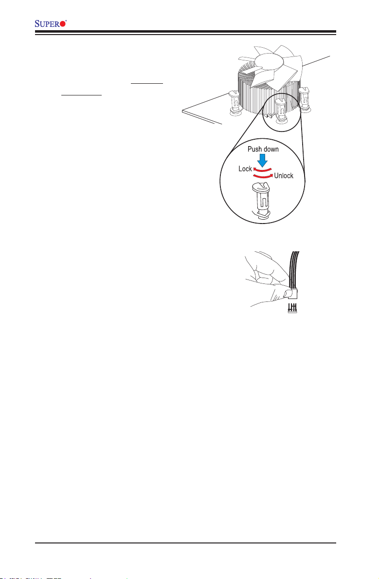
2-8
X9SCM/X9SCM-F/X9SCL/X9SCL-F/X9SCL+-F User’s Manual
motherboard. Gently push the
pairs of diagonal fasteners
(#1 & #2, and #3 & #4) into
the mounting holes until you
hear a click. Also, make sure
to orient each fastener so that
the narrow end of the groove
is pointing outward.
8. Repeat Step 7 to insert all
four heatsink fasteners into
the mounting holes.
9. Once all four fasteners are
securely inserted into the
mounting holes, and the heat-
sink is properly installed on
the motherboard, connect the
heatsink fan wires to the CPU
Fan connector.
Page 33
Chapter 2: Installation
2-9
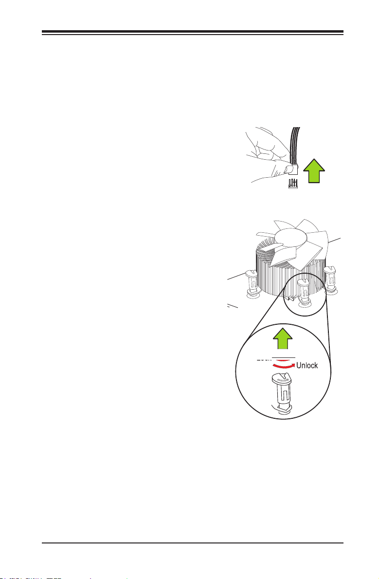
Removing the Heatsink
Warning: We do not recommend that the
CPU or the heatsink be removed. However, if
you do need to remove the heatsink, please
follow the instructions below to remove the
heatsink and to prevent damage done to the
CPU or other components.
Active Heatsink Removal
1. Unplug the power cord from the
power supply.
2. Disconnect the heatsink fan wires
from the CPU fan header.
3. Use your nger tips to gently press
on the fastener cap and turn it
counterclockwise to make a 1/4 (90
0
)
turn, and pull the fastener upward to
loosen it.
4. Repeat Step 3 to loosen all fasteners
from the mounting holes.
5. With all fasteners loosened, remove
the heatsink from the CPU.
Unplug the
PWR cord
Pull Up
Page 34
2-10
X9SCM/X9SCM-F/X9SCL/X9SCL-F/X9SCL+-F User’s Manual
X9SCM/X9SCL(-F) Rev.1.0
2-3 Installing DDR3 Memory
Note: Check the Supermicro website for recommended memory mod-
ules.
CAUTION
Exercise extreme care when installing or removing DIMM
modules to prevent any possible damage.
DIMM Installation
1. Insert the desired number of DIMMs into the memory slots, starting with
DIMM2A. (For best performance, please use the memory modules of the
same type and speed in the same bank.)
2. Push the release tabs outwards on both ends of the DIMM slot to unlock it.
3. Align the key of the DIMM module with the receptive point on the memory
slot.
4. Align the notches on both ends of the module against the receptive points on
the ends of the slot.
Release Tabs
Notches
5. Use two thumbs together to press the notches on both ends of the module
straight down into the slot until the module snaps into place.
Press both notches
straight down into
the memory slot.
6. Press the release tabs to the lock positions to secure the DIMM module into
the slot.
Removing Memory Modules
Reverse the steps above to remove the DIMM modules from the motherboard.
Page 35
Chapter 2: Installation
2-11
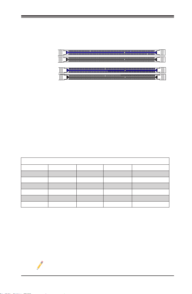
Memory Support
The X9SCM/X9SCL series supports up to 32GB of Unbuffered (UDIMM) DDR3
ECC 1600/1333/1066 MHz DIMMs in 4 memory slots.
DIMM1A
DIMM2A
(Blue Slot)
DIMM2B
(Blue Slot)
DIMM1B
Memory Population Guidelines
When installing memory modules, the DIMM slots should be populated in the following
order: DIMM2A, DIMM2B, DIMM1A and DIMM1B.
• Always use DDR3 DIMM modules of the same size, type and speed.
• Mixed DIMM speeds can be installed. However, all DIMMs will run at the speed
of the slowest DIMM.
• The motherboard will support one DIMM module or three DIMM modules installed,
but it is recommended that a balanced DIMM population (installed in pairs) are
followed for best performance.
Recommended Population (Balanced)
DIMM2A Slot DIMM2B Slot DIMM1A Slot DIMM1B Slot Total System Memory
2GB DIMM 2GB DIMM 4GB
2GB DIMM 2GB DIMM 2GB DIMM 2GB DIMM 8GB
4GB DIMM 4GB DIMM 8GB
4GB DIMM 4GB DIMM 4GB DIMM 4GB DIMM 16GB
8GB DIMM 8GB DIMM 16GB
8GB DIMM 8GB DIMM 8GB DIMM 8GB DIMM 32GB
Note: For memory speed 1600 MHz support, an E3-1200 v2 CPU is
required.
Page 36

2-12
X9SCM/X9SCM-F/X9SCL/X9SCL-F/X9SCL+-F User’s Manual
The table explains the different types of memory supported that can be accomodated
in each memory slot.
DDR3 Unbuffered ECC (UDIMM) Memory
DIMM Slots per
Channel
DIMMs Populat-
ed per Channel
DIMM Type POR Speeds Ranks per DIMM (any
combination)
2 1 Unbuffered
DDR3
1066, 1333 Single Rank, Dual Rank
2 2 Unbuffered
DDR3
1066, 1333 Single Rank, Dual Rank
Note: Due to memory allocation to system devices, the amount of memory that
remains available for operational use will be reduced when 4 GB of R AM is used.
The reduction in memory availability is disproportional.
For Microsoft Windows users: Microsoft implemented a design change in the Win-
dows XP with Service Pack 2 (SP2) and Windows Vista. This change is specic
to the behavior of Physical Address Extension (PAE) mode which improves driver
compatibility. For more information, please read the following article at Microsoft’s
Knowledge Base website at: http://support.microsoft.com/kb/888137.
Possible System Memory Allocation & Availability
System Device Size Physical Memory
Remaining (-Available)
(4 GB Total System
Memory)
Firmware Hub ash memory (System BIOS) 1 MB 3.99
Local APIC 4 KB 3.99
Area Reserved for the chipset 2 MB 3.99
I/O APIC (4 Kbytes) 4 KB 3.99
PCI Enumeration Area 1 256 MB 3.76
PCI Express (256 MB) 256 MB 3.51
PCI Enumeration Area 2 (if needed) -Aligned on 256-MB
boundary-
512 MB 3.01
VGA Memory 16 MB 2.85
TSEG 1 MB 2.84
Memory available to OS and other applications 2.84
Page 37
Chapter 2: Installation
2-13
X9SCM/X9SCL(-F) Rev.1.0
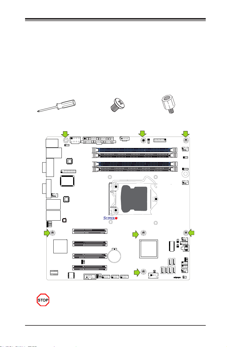
2-4 Motherboard Installation
All motherboards have standard mounting holes to t different types of chassis.
Make sure that the locations of all the mounting holes for both motherboard and
chassis match. Although a chassis may have both plastic and metal mounting fas-
teners, metal ones are highly recommended because they ground the motherboard
to the chassis. Make sure that the metal standoffs click in or are screwed in tightly.
Then use a screwdriver to secure the motherboard onto the motherboard tray.
Tools Needed
Philips Screwdriver
Standoffs
Philips Screwdriver
Location of Mounting Holes
Caution: 1) To prevent damage to the motherboard and its components,
please do not use a force greater than 8 lb/inch on each mounting screw
during motherboard installation. 2) Some components are very close to the
mounting holes. Please take precautionary measures to avoid damaging
these components when installing the motherboard to the chassis.
Page 38

2-14
X9SCM/X9SCM-F/X9SCL/X9SCL-F/X9SCL+-F User’s Manual
Installing the Motherboard
1. Install the I/O shield into the chassis.
2. Locate the mounting holes on the motherboard.
3. Locate the matching mounting holes on the chassis. Align the mounting holes
on the motherboard against the mounting holes on the chassis.
4. Install standoffs in the chassis as needed.
5. Install the motherboard into the chassis carefully to avoid damaging mother-
board components.
6. Using the Philips screwdriver, insert a Pan head #6 screw into a mounting
hole on the motherboard and its matching mounting hole on the chassis.
7. Repeat Step 5 to insert #6 screws into all mounting holes.
8. Make sure that the motherboard is securely placed in the chassis.
Note: Images displayed are for illustration only. Your chassis or compo-
nents might look different from those shown in this manual.
Page 39
Chapter 2: Installation
2-15
X9SCM/X9SCL(-F) Rev.1.0
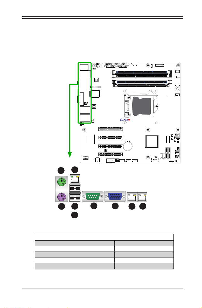
2-5 Connectors/IO Ports
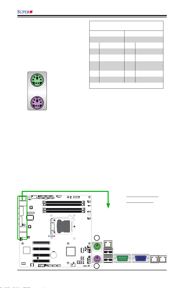
The I/O ports are color coded in conformance with the industry standards. See the
gure below for the colors and locations of the various I/O ports.
Back I/O Panel
1
Back I/O Panel
1. Keyboard (Purple) 6. COM 1
2. PS/2 Mouse (Green) 7. VGA
3. USB Port 0 8. LAN1
4. USB Port 1 9. LAN2
5. IPMI LAN (X9SCM-F/X9SCL-F/X9SCL+-F Only)
2
3
4
5
6
7
8
9
Page 40
2-16
X9SCM/X9SCM-F/X9SCL/X9SCL-F/X9SCL+-F User’s Manual
ATX PS/2 Keyboard/Mouse
Ports
The ATX PS/2 keyboard and
PS/2 mouse are located next to
the Back Panel USB Ports 0/1 on
the motherboard. See the table at
right for pin denitions.
PS/2 Keyboard/Mouse Pin
Denitions
PS2 Keyboard PS2 Mouse
Pin# Denition Pin# Denition
1 KB Data 1 Mouse Data
2 No Connection 2 No Connection
3 Ground 3 Ground
4 Mouse/KB VCC
(+5V)
4 Mouse/KB VCC
(+5V)
5 KB Clock 5 Mouse Clock
6 No Connection 6 No Connection
VCC: with 1.5A PTC (current limit)
1. Keyboard (Purple)
2. Mouse (Green)
Keyboard
Mouse
X9SCM/X9SCL(-F) Rev.1.0
1
2
Page 41
Chapter 2: Installation
2-17
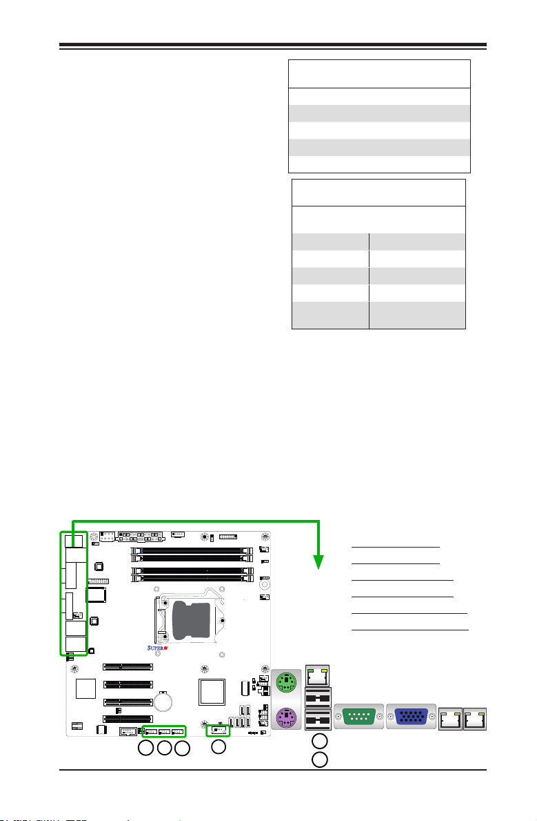
1. Backpanel USB 0
2. Backpanel USB 1
3. Front Panel USB 2/3
4. Front Panel USB 4/5
5. Front Panel USB 12/13
6. Internal 'Type A' USB 11
Universal Serial Bus (USB)
Two Universal Serial Bus ports (USB
0/1) are located on the I/O back panel.
In addition, six USB connections (USB
2/3, USB 4/5, USB 12/13) are used to
provide front chassis access. USB 11
is a Type A Connector. (USB Cables
are not included). See the tables on
the right for pin denitions.
Back Panel USB 0/1
Pin Denitions
Pin# Denition Pin# Denition
1 +5V 5 +5V
2 USB_PN0 6 USB_PN1
3 USB_PP0 7 USB_PP1
4 Ground 8 Ground
Front Panel USB 2/3, 4/5, 12/13
Pin Denitions
USB 2/4/12/11
Pin # Denition
USB 3/5/13
Pin # Denition
1 +5V 6 +5V
2 USB_PN2 7 USB_PN3
3 USB_PP2 8 USB_PP3
4 Ground 9 Ground
5 No Con-
nection
10 Key
4
3
5
X9SCM/X9SCL(-F) Rev.1.0
6
1
2
Page 42

2-18
X9SCM/X9SCM-F/X9SCL/X9SCL-F/X9SCL+-F User’s Manual
Ethernet Ports
Two Ethernet ports (LAN1/LAN2) are
located next to the VGA port on the
I/O Backpanel. In addition, an IPMI
Dedicated LAN is also located above
USB 0/1 ports on the X9SCM-F/
X9SCL-F/X9SCL+-F to provide a
dedicated network connection for
IPMI 2.0. These ports accept RJ45
type cables.
Notes:
1. The IPMI Dedicated LAN
is for the X9SCM-F/X9SCL-
F/X9SCL+-F only.
2. Please refer to the LED
Indicator Section for LAN
LED information.
1. LAN1
2. LAN2
3.IPMI Dedicated LAN (X9SCM-F/
X9SCL-F/X9SCL+-F only)
1
2
X9SCM/X9SCL(-F) Rev.1.0
3
LAN Ports
Pin Denition
Pin# Denition
1 TD0- 10 SGND
2 TD0+ 11 P3V3SB
3 TD1- 12 Act LED
4 TD1+ 13 Link 100 LED
(Green, +3V3SB)
5 TD2- 14 Link 1000 LED
(Yellow, +3V3SB)
6 TD2+ 15 Ground
7 TD3- 16 Ground
8 TD3+ 17 Ground
9 P2V5SB 88 Ground
(NC: No Connection)
Page 43

Chapter 2: Installation
2-19
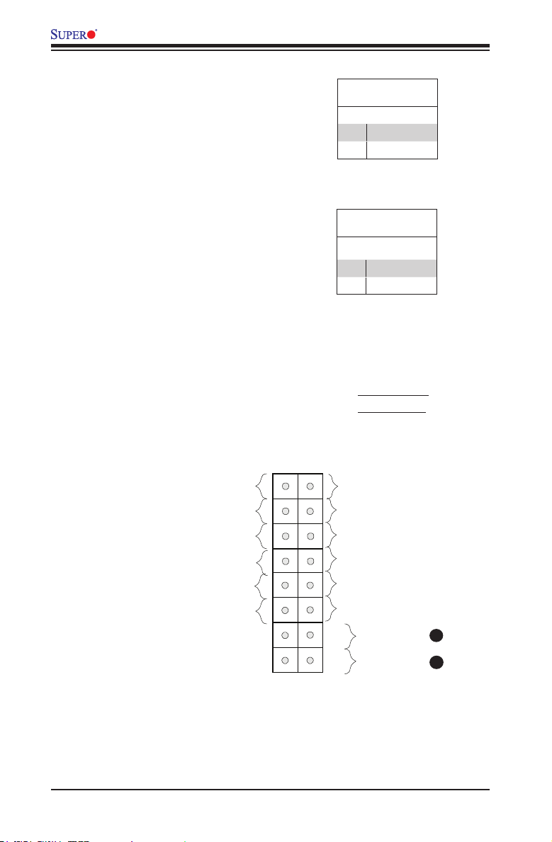
Serial Ports
A COM Port (COM1) is located on
the I/O bac kpan el, and anoth er Ser ial
Connection (COM2) is located below
PCI-E Slot4 to provide front access.
See the table on the right for pin
denitions.
Serial Port Pin Denitions
(COM1/COM2)
Pin # Denition Pin # Denition
1 DCD 6 DSR
2 RXD 7 RTS
3 TXD 8 CTS
4 DTR 9 RI
5 Ground 10 NC
1. COM1
2. COM2
X9SCM/X9SCL(-F) Rev.1.0
1
2
Page 44

2-20
X9SCM/X9SCM-F/X9SCL/X9SCL-F/X9SCL+-F User’s Manual
1. VGA
Video Connector
A Video (VGA) connector is located
next to the COM Port on the I/O
backpanel. This connector is used
to provide video and CRT display.
Refer to the board layout below for
the location.
VGA/CRT Pin
Denitions
Pin# Denition Pin# Denition
1 Red 10 Ground
2 Green 11 NC
3 Blue 12 MS1: SDA (DDC Data)
4 NC 13 HSYNC
5 Ground 14 VSYSNC
6 Ground 15 MS3: SCL (DDC CLK)
7 Ground 16 Case
8 Ground 17 Case
9 5V
NC= No Connection
1
X9SCM/X9SCL(-F) Rev.1.0
Page 45

Chapter 2: Installation
2-21
Front Control Panel
JF1 contains header pins for various buttons and indicators that are normally lo-
cated on a control panel at the front of the chassis. These connectors are designed
specically for use with Supermicro server chassis. See the gure below for the
descriptions of the various control panel buttons and LED indicators. Refer to the
following section for descriptions and pin denitions.
Pin 15Pin 16
Pin 1
Pin 2
X9SCM/X9SCL(-F) Rev.1.0
JF1 Header Pins
Power Button
OH/Fan Fail LED
1
NIC1 LED
Reset Button
2
HDD LED
Power LED
Reset
PWR
LED_Anode+
LED_Anode+
LED_Anode+
UID LED
Ground
Ground
Power Fail LED
NIC2 LED
LED_Anode+
LED_Anode+
Page 46

2-22
X9SCM/X9SCM-F/X9SCL/X9SCL-F/X9SCL+-F User’s Manual
Front Control Panel Pin Denitions
Power LED
The Power LED connection is located
on pins 15 and 16 of JF1. Refer to the
table on the right for pin denitions.
Power LED
Pin Denitions (JF1)
Pin# Denition
15 3.3V/vcc
16 Ground
A. PWR LED
B. HDD LED
HDD LED
The HDD LED connection is located
on pins 13 and 14 of JF1. Attach a
cable here to indicate the status of
HDD-related activities, including IDE,
SATA activities. See the table on the
right for pin denitions.
HDD LED
Pin Denitions (JF1)
Pin# Denition
13 3.3V/vcc
14 HD Active
Power Button
OH/Fan Fail LED
1
NIC1 LED
Reset Button
2
HDD LED
Power LED
Reset
PWR
LED_Anode+
LED_Anode+
LED_Anode+
UID LED
Ground
Ground
Power Fail LED
NIC2 LED
LED_Anode+
LED_Anode+
A
B
Page 47

Chapter 2: Installation
2-23
NIC1/NIC2 (LAN1/LAN2)
The NIC (Network Interface Controller)
LED connection for LAN port 1 is located
on pins 11 and 12 of JF1, and the LED
connection for LAN Port 2 is on Pins 9
and 10. NIC1 LED and NIC2 LED are
2-pin NIC LED headers. Attach NIC LED
cables to NIC1 and NIC2 LED indicators
to display network activities. Refer to the
table on the right for pin denitions.
LAN1/LAN2 LED
Pin Denitions (JF1)
Pin# Denition
9/11 Vcc
10/12 LAN Active
A. NIC1 LED
B. NIC2 LED
C. OH/Fan Fail/UID LED
Overheat (OH)/Fan Fail/Front UID LED
Connect an LED cable to the Front UID and
OH/Fan Fail connections on pins 7 and 8
of JF1 to display UID (Unit ID) signals or
to provide advanced warnings for chassis
overheat/fan failure. Refer to the table on
the right for pin de nitions.
OH/Fan Fail LED
Pin Denitions (JF1)
Pin# Denition
7 Vcc/Blue UID LED
8 OH/Fan Fail LED
OH/Fan Fail Indicator
Status
State Denition
Off Normal
On Overheat
Flash-
ing
Fan Fail
C
A
B
Power Button
OH/Fan Fail LED
1
NIC1 LED
Reset Button
2
HDD LED
Power LED
Reset
PWR
LED_Anode+
LED_Anode+
LED_Anode+
UID LED
Ground
Ground
Power Fail LED
NIC2 LED
LED_Anode+
LED_Anode+
Page 48
2-24
X9SCM/X9SCM-F/X9SCL/X9SCL-F/X9SCL+-F User’s Manual
Power Button
The Power Button connection is located
on pins1 and 2 of JF1. Momentarily con-
tacting both pins will power on/off the sys-
tem. This button can also be congured
to function as a suspend button (with a
setting in the BIOS - see Chapter 4). To
turn off the power in the suspend mode,
press the button for at least 4 seconds.
Refer to the table on the right for pin
denitions.
Power Button
Pin Denitions (JF1)
Pin# Denition
1 Signal
2 Ground
Reset Button
The Reset Button connection is located
on pins 3 and 4 of JF1. Attach it to a
hardware reset switch on the computer
case to reset the system. Refer to the
table on the right for pin denitions.
Reset Button
Pin Denitions (JF1)
Pin# Denition
3 Reset
4 Ground
A. Reset Button
B. PWR Button
A
B
Power Button
OH/Fan Fail LED
1
NIC1 LED
Reset Button
2
HDD LED
Power LED
Reset
PWR
LED_Anode+
LED_Anode+
LED_Anode+
UID LED
Ground
Ground
Power Fail LED
NIC2 LED
LED_Anode+
LED_Anode+
Page 49

Chapter 2: Installation
2-25
J31
JTPM
J29
JL1
JI2C2
JI2C1
T-SGPIO1
JWF1
JPW2
JWOL
JSPK
JPI2C
JPW1
COM1
SPKR1
JBT1
LE2
JWD
JLED1
JPL2
JPG1
JPB
JPL1
JPUSB1
FAN1
FANA
FAN3
FAN2
USB4/5
USB 12/13
_LAN
IPMI
COM2
VGA
USB11
DIMM2B
DIMM2A
USB2/3
Slot6 PCI-E 3.0/2.0 x8
JF1
I-SATA2
Slot4 PCI-E 2.0 x4 on x8
KB/MOUSE
DIMM1B
DIMM1A
CPU
Slot7 PCI-E 3.0/2.0 x8
BIOS
B1
Battery
LAN
BMC
CTRL
S I/O
T-SGPIO2
FP CTRL
Cougar Point
Standard PCH
Memory Chip
Fan4
LAN
(*I-SATA 0/1: SATA3)
I-SATA4
I-SATA5
I-SATA3
I-SATA1
I-SATA0
Slot5 PCI-E 2.0 x4 on x8
USB/0/1
LAN1
LAN2
LE7
JPME1
JPME2
LE4
LAN
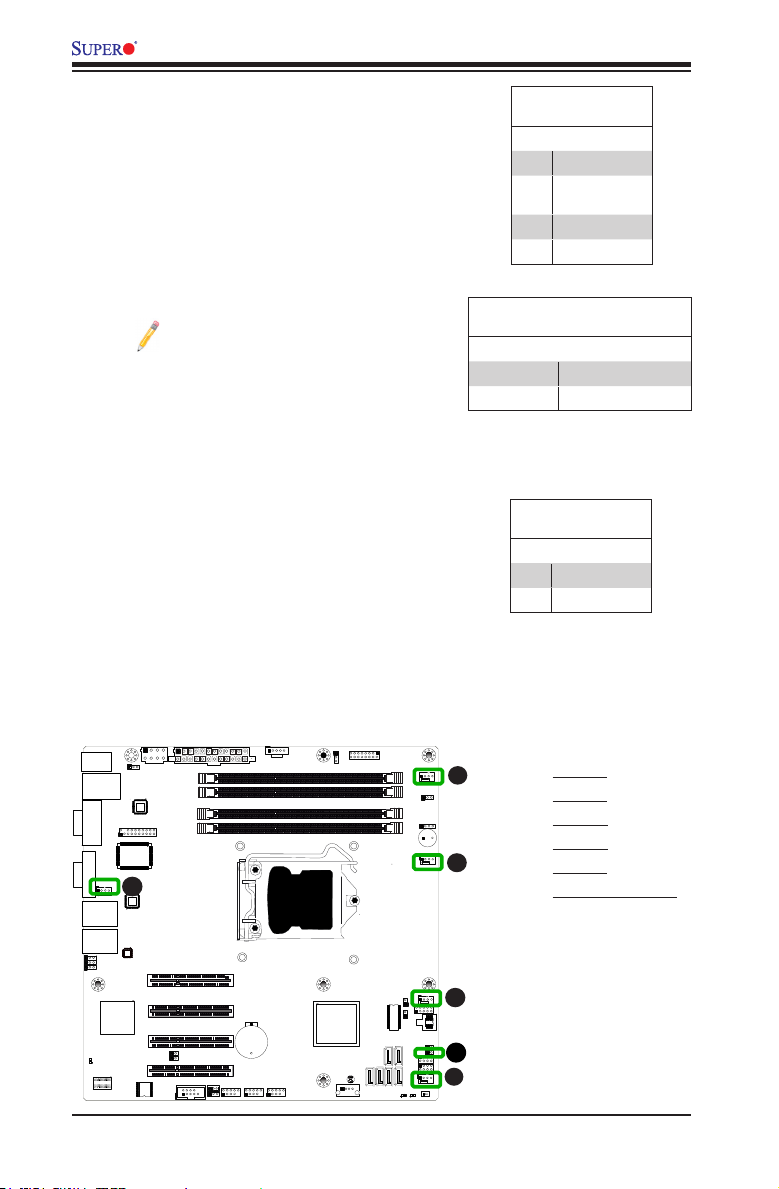
2-6 Connecting Cables
This section provides brief descriptions and pin-out denitions for onboard headers
and connectors. Be sure to use the correct cable for each header or connector. For
information on Backpanel USB and Front Panel USB ports, refer to Page 2-17. For
COM Port 1 and COM Port 2, please see Page 2-19.
A. 24-Pin ATX Main PWR
B. 8-Pin Processor PWR
A
B
ATX Power 24-pin Connector
Pin Denitions (JPW1)
Pin# Denition Pin # Denition
13 +3.3V 1 +3.3V
14 -12V 2 +3.3V
15 COM 3 COM
16 PS_ON 4 +5V
17 COM 5 COM
18 COM 6 +5V
19 COM 7 COM
20 Res (NC) 8 PWR_OK
21 +5V 9 5VSB
22 +5V 10 +12V
23 +5V 11 +12V
24 COM 12 +3.3V
(Required)
12V 8-pin Power Connec-
tor Pin Denitions
Pins Denition
1 through 4 Ground
5 through 8 +12V
ATX Main PWR & CPU PWR
Connectors
The 24-pin main power connector
(JPW1) is used to provide power to
the motherboard. The 8-pin connector
(JPW2) is also required for the proces-
sor. These power connectors meet the
SS I EPS 12V spe ci c at ion . See the ta ble
on the ri ght for pin de niti ons . Note: The
8-pin JPW2 will also support one 4-pin
power connector.
8-Pin/4-pin Processor PWR
A
B
24-Pin Main PWR
Page 50
2-26
X9SCM/X9SCM-F/X9SCL/X9SCL-F/X9SCL+-F User’s Manual
J31
JTPM
J29
JL1
JI2C2
JI2C1
T-SGPIO1
JWF1
JPW2
JWOL
JSPK
JPI2C
JPW1
COM1
SPKR1
JBT1
LE2
JWD
JLED1
JPL2
JPG1
JPB
JPL1
JPUSB1
FAN1
FANA
FAN3
FAN2
USB4/5
USB 12/13
_LAN
IPMI
COM2
VGA
USB11
DIMM2B
DIMM2A
USB2/3
Slot6 PCI-E 3.0/2.0 x8
JF1
I-SATA2
Slot4 PCI-E 2.0 x4 on x8
KB/MOUSE
DIMM1B
DIMM1A
CPU
Slot7 PCI-E 3.0/2.0 x8
BIOS
B1
Battery
LAN
BMC
CTRL
S I/O
T-SGPIO2
FP CTRL
Cougar Point
Standard PCH
Memory Chip
Fan4
LAN
(*I-SATA 0/1: SATA3)
I-SATA4
I-SATA5
I-SATA3
I-SATA1
I-SATA0
Slot5 PCI-E 2.0 x4 on x8
USB/0/1
LAN1
LAN2
LE7
JPME1
JPME2
LE4
LAN
Fan Header
Pin Denitions
Pin# Denition
1 Ground (Black)
2 2.5A/+12V
(Red)
3 Tachometer
4 PWM_Control
Fan Headers
The X9SCM/X9SCM-F/X9SCL/X9SCL-F/
X9SCL+-F has ve fan headers (Fan 1~Fan
4 and Fan A). These are 4-pin fan headers. A
fan speed control setting in the BIOS Hardware
Monitoring section allows the BIOS to auto-
matically set fan speeds based on the system
temperature. Refer to the table on the right for
pin denitions and fan designations.
Note: Please use 4-pin fans only.
Though 3-pin fans will still work on
this motherboard, they will only run at
full speed and cannot be automatically
controlled.
A
B
A. Fan 1
B. Fan 2
C. Fan 3
D. Fan 4
E. Fan A
F. Chassis Intrusion
C
D
E
F
Chassis Intrusion
A Chassis Intrusion header is located at JL1 on
the motherboard. Attach the appropriate cable
from the chassis to inform you of a chassis intru-
sion when the chassis is opened.
Chassis Intrusion
Pin Denitions (JL1)
Pin# Denition
1 Intrusion Input
2 Ground
Fan Header
Designations
Fan# Use with
Fan1-Fan4 CPU/Memory Zone
FanA I/O/Add-on Cards
 Loading...