

Page 1

iNTeL 1sT GeN. dCPMM MeMory
CoNfiGUraTioN
for
sUPerMiCro X11oPX/X11QPX/
X11dPX/X11sPX MoTherboards
User's GUide
Revision 1.00
Page 2

The information in this user’s guide has been carefully reviewed and is believed to be accurate. The manufacturer
!
assumes no responsibility for any inaccuracies that may be contained in this document, and makes no commitment
to update or to keep current the information in this manual, or to notify any person or organization of the updates.
Please Note: For the most up-to-date version of this manual, please see our website at www.supermicro.com.
Super Micro Computer, Inc. ("Supermicro") reserves the right to make changes to the product described in this manual
at any time and without notice. This product, including software and documentation, is the property of Supermicro and/
or its licensors, and is supplied only under a license. Any use or reproduction of this product is not allowed, except
as expressly permitted by the terms of said license.
IN NO EVENT WILL Super Micro Computer, Inc. BE LIABLE FOR DIRECT, INDIRECT, SPECIAL, INCIDENTAL,
SPECULATIVE OR CONSEQUENTIAL DAMAGES ARISING FROM THE USE OR INABILITY TO USE THIS PRODUCT
OR DOCUMENTATION, EVEN IF ADVISED OF THE POSSIBILITY OF SUCH DAMAGES. IN PARTICULAR, SUPER
MICRO COMPUTER, INC. SHALL NOT HAVE LIABILITY FOR ANY HARDWARE, SOFTWARE, OR DATA STORED
OR USED WITH THE PRODUCT, INCLUDING THE COSTS OF REPAIRING, REPLACING, INTEGRATING,
INSTALLING OR RECOVERING SUCH HARDWARE, SOFTWARE, OR DATA.
Any disputes arising between manufacturer and customer shall be governed by the laws of Santa Clara County in the
State of California, USA. The State of California, County of Santa Clara shall be the exclusive venue for the resolution
of any such disputes. Supermicro's total liability for all claims will not exceed the price paid for the hardware product.
FCC Statement: This equipment has been tested and found to comply with the limits for a Class A digital device
pursuant to Part 15 of the FCC Rules. These limits are designed to provide reasonable protection against harmful
interference when the equipment is operated in a commercial environment. This equipment generates, uses, and can
radiate radio frequency energy and, if not installed and used in accordance with the manufacturer’s instruction manual,
may cause harmful interference with radio communications. Operation of this equipment in a residential area is likely
to cause harmful interference, in which case you will be required to correct the interference at your own expense.
California Best Management Practices Regulations for Perchlorate Materials: This Perchlorate warning applies only
to products containing CR (Manganese Dioxide) Lithium coin cells. “Perchlorate Material-special handling may apply.
See www.dtsc.ca.gov/hazardouswaste/perchlorate”.
WARNING: This product can expose you to chemicals including
lead, known to the State of California to cause cancer and birth
defects or other reproductive harm. For more information, go
to www.P65Warnings.ca.gov.
The products sold by Supermicro are not intended for and will not be used in life support systems, medical equipment,
nuclear facilities or systems, aircraft, aircraft devices, aircraft/emergency communication devices or other critical
systems whose failure to perform be reasonably expected to result in signicant injury or loss of life or catastrophic
property damage. Accordingly, Supermicro disclaims any and all liability, and should buyer use or sell such products
for use in such ultra-hazardous applications, it does so entirely at its own risk. Furthermore, buyer agrees to fully
indemnify, defend and hold Supermicro harmless for and against any and all claims, demands, actions, litigation, and
proceedings of any kind arising out of or related to such ultra-hazardous use or sale.
Manual Revision 1.00
Release Date: December 6, 2019
Unless you request and receive written permission from Super Micro Computer, Inc., you may not copy any part of this
document. Information in this document is subject to change without notice. Other products and companies referred
to herein are trademarks or registered trademarks of their respective companies or mark holders.
Copyright © 2019 by Super Micro Computer, Inc.
All rights reserved.
Printed in the United States of America
Page 3
Preface
Preface
This user's guide is written for system integrators, IT technicians and knowledgeable end
users. It provides information for the installation and use of 1st Generation Intel® Optane™
DC Persistent Memory Modules (DCPMMs) in a system based on the Supermicro X11OPx/
X11QPx/X11DPx/X11SPx series motherboard.
About This User's Guide
This user's guide provides an introduction to Intel 1st Gen. DC Persistent Memory Modules
(DCPMMs). It also provides detailed instructions on how to install and congure 1st Gen.
DCPMMs on Supermicro X11OPx/X11QPx/X11DPx/X11SPx series motherboards.
User's Guide Organization
Chapter 1 describes the features, specications and performance of Intel 1st Gen. DCPMM
memory modules.
Chapter 2 provides detailed instructions on how to install DCPMM memory in a Supermicro
computer system based on the X11OPx/X11QPx/X11DPx/X11SPx series motherboard.
Chapter 3 provides DCPMM conguration instructions using ipmctl and ndtcl. Read this
chapter when you want to congure the DCPMM settings using the open source utilities
available on the market.
Chapter 4 provides detailed instructions on how to congure DCPMM settings using the
BIOS utility.
Conventions Used in the User's Guide
Special attention should be given to the following symbols to ensure proper installation and
to avoid damaging system components or causing bodily injury to yourself:
Important: Important information given to ensure proper system installation or to relay
safety precautions.
Note: Additional Information given to provide information for proper system setup.
Important Links
For your system to work properly, please follow the links below to download all necessary
drivers/utilities and the user’s guide for your system.
• Supermicro product manuals: http://www.supermicro.com/support/manuals/
• Product drivers and utilities: https://www.supermicro.com/wftp/driver
• Product safety info: http://www.supermicro.com/about/policies/safety_information.cfm
• If you have any questions, please contact our support team at: support@supermicro.com
3
Page 4

Super 1st Gen. DCPMM Memory for X11OPx/X11QPx/X11DPx/X11SPx Motherboards Guide
Contacting Supermicro
Headquarters
Address: Super Micro Computer, Inc.
980 Rock Ave.
San Jose, CA 95131 U.S.A.
Tel: +1 (408) 503-8000
Fax: +1 (408) 503-8008
Email: marketing@supermicro.com (General Information)
support@supermicro.com (Technical Support)
Website: www.supermicro.com
Europe
Address: Super Micro Computer B.V.
Het Sterrenbeeld 28, 5215 ML
's-Hertogenbosch, The Netherlands
Tel: +31 (0) 73-6400390
Fax: +31 (0) 73-6416525
Email: sales@supermicro.nl (General Information)
support@supermicro.nl (Technical Support)
rma@supermicro.nl (Customer Support)
Website: www.supermicro.nl
Asia-Pacic
Address: Super Micro Computer, Inc.
3F, No. 150, Jian 1st Rd.
Zhonghe Dist., New Taipei City 235
Taiwan (R.O.C)
Tel: +886-(2) 8226-3990
Fax: +886-(2) 8226-3992
Email: support@supermicro.com.tw
Website: www.supermicro.com.tw
4
Page 5

Preface
Table of Contents
Chapter 1 Introduction
1.1 Introduction to Intel 1st Gen. DCPMM Memory Modules ....................................................6
1.2 DCPMM Modes ....................................................................................................................7
1.3 Specications .......................................................................................................................7
Chapter 2 DCPMM Memory Installation
2.1 Static-Sensitive Devices .....................................................................................................10
2.2 Installing DCPMM Memory Modules .................................................................................. 11
Chapter 3 Conguring DCPMM Settings Using Open Source Utilities
3.1 DCPMM Conguration........................................................................................................30
3.2 Ipmctl Conguration ...........................................................................................................32
Chapter 4 Conguring DCPMM Settings Using BIOS
4.1 To Enter the BIOS Setup Utility..........................................................................................42
4.2 To Congure DCPMM Memory as App Direct Mode .........................................................45
4.3 To Congure DCPMM Memory as Memory Mode .............................................................51
4.4 To Congure DCPMM Memory as Mixed Memory Mode ..................................................53
5
Page 6

Super 1st Gen. DCPMM Memory for X11OPx/X11QPx/X11DPx/X11SPx Motherboards Guide
Chapter 1
Introduction
Congratulations on purchasing your motherboard or your system from an industry leader.
Supermicro products are designed to provide you with the highest standards in quality and
performance.
1.1 Introduction to Intel 1st Gen. DCPMM Memory Modules
Intel® 1st Gen. Optane™ DC Persistent Memory Module (DCPMM), the latest memory
innovation, provides a new data-centric architecture that offers increased storage capabilities
for higher performance computing platforms with exible conguration options at lower cost.
Utilizing the unique disruptive technology, DCPMM can operate as system memory, which
allows the DCPMM to have memory-like performance with the storage capacity of a solid state
drive. In addition, DCPMM can also function as storage, providing memory-like performance
with persistence and high-capacity while operating at much lower latency at an affordable cost.
DCPMM memory supports three modes: Memory Mode, App Direct Mode, and Mixed Mode.
Optimized for volatile use, Memory Mode provides a high-capacity main memory solution
with higher power efciency at lower operational cost. All installed DDR4 DIMMs are hidden
from the operating system and act as the caching layer for the portion of the DCPMMs.
Featuring byte-addressability and cache-coherence, App Direct Mode allows memory space
to be provisioned as persistent memory where software can "talk directly to" the persistent
memory in the "byte-addressable" manner without any modications needed. DCPMM also
offers Mixed Memory Mode, a combination of Memory Mode and App Direct Mode, which
will allow a portion of the DCPMM to be used for the Memory Mode operations, while the
remaining portion is used for the App Direct Mode operations. This is especially instrumental
for the applications that use system RAM for in-memory databases. With DCPMM memory
used in the system, there is no need for the system RAM to copy data from disk to memory,
and thus effectively eliminate in-memory database initialization delays at bootup, further
enhancing system performance.
6
Page 7

Chapter 1: Introduction
1.2 DCPMM Modes
This section provides additional details on DCPMM modes. Please refer to the information
below to congure your DCPMM memory settings.
Memory Mode (volatile memory)
In Memory Mode, the system treats DCPMM modules as system memory, and DCPMMs
will act as large-capacity DDR4 memory modules. The installed DDR4 DIMMs will become
a caching layer for the DCPMMs and will be hidden from the operating system.
App Direct Mode (non-volatile memory)
In App Direct Mode, DCPMM modules provide all persistent memory features to the
operating system and to the applications that support them. The DDR4 DIMMs will act as
system memory and DCPMMs will act as persistent storage.
Mixed Mode
DCPMMs can be congurated in Mixed Memory Mode with a portion of their capacity used
for Memory Mode operations, and the remaining capacity as persistent memory for App
Direct Mode operations. All DDR4 DIMMs discovered in the system are hidden from the
operating system and act as a caching layer for the DCPMMs Memory Mode portion.
Memory Ratio
In Memory Mode and Mixed Mode congurations, the required ratio of system memory to
DCPMMs is between 1:16 and 1:4 gigabytes. In order to achieve the best performance,
a ratio of 1:4 is recommended. In Mixed Mode, this ratio requirement applies to system
memory and only the volatile portion of the DCPMMs. The ratio requirement does not apply
to App Direct Mode.
1.3Specications
Operating Speed
1st Gen. DCPMMs operate at 2666 MHz DDR4 memory bus speed, and any installed 2933
MHz DDR4 memory will also operate at 2666 MHz.
Capacity
1st Gen. DCPMM modules are offered in capacities of 128GB, 256GB, and 512GB.
7
Page 8

Super 1st Gen. DCPMM Memory for X11OPx/X11QPx/X11DPx/X11SPx Motherboards Guide
AdditionalSpecications
When set to App-Direct Mode, DCPMM provides optional data security support, including
secure-erasing and data-encryption. DCPMM encrypts data using AES 256-bit encryption
and it supports the following memory functions:
ECC
ECC (Error-Correcting Code) memory, a type of computer data storage, can detect and
correct most-common internal data corruptions and errors. ECC memory is usually used in
computers that cannot tolerate data corruptions or memory errors such as computers used
for scientic or nancial purposes. Normally, ECC memory maintains a memory system
that is immune to single-bit errors so that the data that is read from each word is always
the same as the data that had been written to it. ECC memory will protect against any
additional memory failure caused by a ‘single-bit’ error in the same memory rank.
SDDC
SDDC (Single Device Data Correction) checks and corrects single-bit or multiple-bit (4-bit
max.) memory corruptions and errors that affect an entire single x4 DRAM device. SDDC
Plus One is the enhanced feature to SDDC. Using this enhanced feature will spare the
faulty DRAM device out after an SDDC event has occurred. After the event, ECC mode will
be activated to further protect the system against any additional memory failure caused by
a ‘single-bit’ error in the same memory rank.
DDDC
DDDC (Double Device Data Correction) provides memory-error checking and correction and
it also prevents the system from issuing a performance penalty before a device fails. Please
note that virtual lockstep mode might be affected until a faulty DRAM module is spared.
Patrol scrubbing
Patrol Scrubbing is a process that allows the CPU to correct correctable memory errors
detected on a memory module and send the correction to the requestor (the original source).
When Patrol Scrubbing is activated, the IO hub will read and write back one cache line
every 16K cycles if there is no delay caused by internal processing. By using this method,
roughly 64 GB of memory behind the IO hub will be scrubbed every day.
Demand scrubbing
Demand Scrubbing is a process that allows the CPU to correct correctable memory errors
found on a memory module. When the CPU or I/O issues a demand-read command, and the
read data from memory turns out to be a correctable error, the error is corrected and sent
to the requestor (the original source). In the meantime, system memory is updated as well.
8
Page 9

Operating System Support
1st Gen. DCPMM modules support the following operation systems:
• Microsoft Windows Server 2019
• Red Hat Enterprise Linux 7.6
• SUSE Linux Enterprise Server 12.4
• SUSE Linux Enterprise Server 15
• VMware vSphere Hypervisor (ESXi) 6.7 U1
• Ubuntu LTS 18.04
Processor Platform Support
Chapter 1: Introduction
1st Gen. DCPMM modules are supported by the following processors:
• 2nd Gen Intel® Xeon Scalable-SP (82xx/62xx/52xx/4215 series) processors
Platform Support
• 1st Gen. DCPMM memory supports Supermicro X11OPx, X11QPx, X11DPx and X11SPx*
series of motherboards. (*See the note below.)
Note: For the X11SPx motherboards, only X11SPL-F (rev. 1.03) and X11SPM-F/TF/
TPF (all revisions) have been validated for DCPMM memory support.
9
Page 10

Super 1st Gen. DCPMM Memory for X11OPx/X11QPx/X11DPx/X11SPx Motherboards Guide
Chapter 2
DCPMM Memory Installation
2.1 Static-Sensitive Devices
Electrostatic Discharge (ESD) can damage electronic com ponents. To avoid damaging your
motherboard, it is important to handle it very carefully. The following measures are generally
sufcient to protect your equipment from ESD.
Precautions
• Use a grounded wrist strap designed to prevent static discharge.
• Touch a grounded metal object before removing the motherboard from the antistatic bag.
• Handle the motherboard by its edges only; do not touch its components, peripheral chips,
memory modules or gold contacts.
• When handling chips or modules, avoid touching their pins.
• Put the motherboard and peripherals back into their antistatic bags when not in use.
• For grounding purposes, make sure that your computer chassis provides excellent conduc-
tivity between the power supply, the case, the mounting fasteners and the motherboard.
• Use only the correct type of onboard CMOS battery. Do not install the onboard battery
upside down to avoid possible explosion.
Unpacking
Supermicro's motherboards are shipped in antistatic packaging to avoid static damage. When
unpacking a motherboard , make sure that the person handling it is static protected.
10
Page 11

Chapter 2: DCPMM Memory Installation
2.2 Installing DCPMM Memory Modules
Important: Exercise extreme care when installing or removing DIMM modules to pre-
vent any possible damage.
Memory Population Requirements
For proper memory installation, please pay close attention to the following instructions:
1. Intel 1st Generation DCPMM is supported by Supermicro X11OPx, X11QPx, X11DPx,
X11SPx series motherboards.
2. Memory speeds are dependent upon the processors used in your system.
3. All DCPMMs installed on your motherboard must be of the same size, and the DDR4
DIMMs that are installed in conjunction with DCPMMs must be of the same size and the
same type as well.
4. When installing a memory module, be sure to install the DIMM module in the rst
channel slot (i.e. DIMMA1), and then, in the second channel slot (i.e. DIMMA2).
5. Please use balanced conguration to achieve maximum performance. Supermicro
does not recommend unbalanced memory conguration since it will reduce memory
performance.
6. Mixing different DIMM types or using 1Rx8 DIMMs in conjunction with DCPMMs is not
supported.
7. A total of six DCPMMs can be supported per processor (one in each memory channel),
and a minimum of two DDR4 DIMMs are required per processor (one per memory
controller).
8. For Memory Mode, a minimum of two DCPMMs are required per processor (one per
memory controller). For App Direct Mode, a minimum of one DCPMM is required per
processor (any processor).
9. Check the Supermicro website for recommended memory modules.
11
Page 12

Super 1st Gen. DCPMM Memory for X11OPx/X11QPx/X11DPx/X11SPx Motherboards Guide
Maximum Memory Capacity Supported on a Platform
The maximum memory capacity that is supported on a platform is dependent on the sufx of
the Second Generation Xeon Scalable Processor used in your system:
• Processors with an L sufx (i.e. 8280L): 4.5 TB maximum per processor
• Processors with an M sufx (i.e. 8280M): 2 TB maximum per processor
• Processors with no sufx (i.e. 8280): 1 TB per processor
RestrictionsonMemoryCongurationSettings
When conguring memory mirroring and memory sparing settings, please note the following
restrictions:
1. Only the DRAM DIMM installed in the system will be mirrored; DCPMMs do not support
memory mirroring.
2. Memory mirroring is only supported when DCPMMs are congured in App-Direct Mode.
3. Memory sparing is not supported when DCPMMs are installed in the system.
12
Page 13
Chapter 2: DCPMM Memory Installation
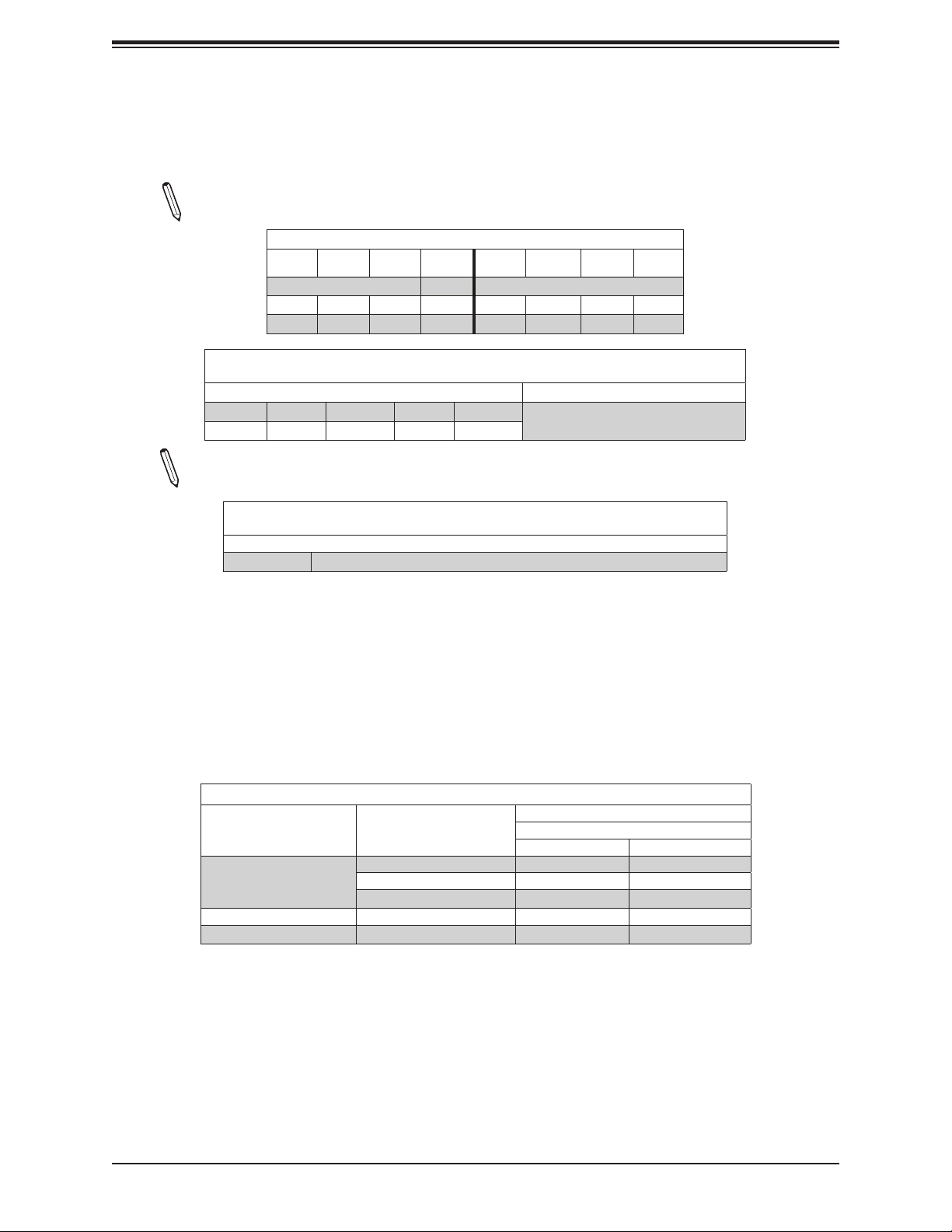
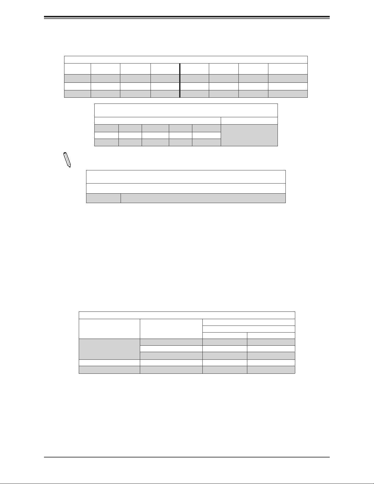
DCPMM Population Tables
DCPMM Population Table for the X11UP Motherboards (w/6 DIMM slots)
Note: The following tables are supported supported by the X11SPM-F/TF/TPF only.
Symmetric Population within CPU Socket
Modes DIMMC1 DIMMB1 DIMMA1 DIMMD1 DIMME1 DIMMF1
AD DCPMM DRAM1 DRAM1 DRAM1 DRAM1 DCPMM 1-1-1
MM DCPMM DRAM1 DRAM1 DRAM1 DRAM1 DCPMM 1-1-1
AD + MM DCPMM DRAM3 DRAM3 DRAM3 DRAM3 DCPMM 1-1-1
Channel
Cong.
(for the two tables above)
DDR4 Type Capacity
DRAM1 RDIMM 3DS RDIMM LRDIMM 3DS LRDIMM
DRAM3 RDIMM 3DS RDIMM LRDIMM -
Legend
Refer to Validation Matrix (DDR4 DIMMs validated
with DCPMM) below.
Note: DDR4 single rank x8 is not available for DCPMM Memory Mode or App-Direct
Mode.
(forthersttwotables above)
DCPMM Any Capacity (Uniformly for all channels for a given conguration)
Legend
Capacity
• For each individual population, rearrangements between channels are allowed as long as the resulting population is
compliant with the Supermicro X11OPx/X11QPx/X11DPx/X11SPx memory population rules for the 2nd Gen Intel Xeon
Scalable-SP (82xx/62xx/52xx/4215 series) processors.
• For each individual population, please use the same DDR4 DIMM in all slots.
• For each individual population, sockets are normally symmetric with exceptions for 1 DCPMM per socket and 1 DCPMM
per node case. Currently, DCPMM modules operate at 2666 MHz.
• No mixing of DCPMM and NVMDIMMs within the same platform is allowed.
• This DCPMM population guide targets a balanced DCPMM-to-DRAM-cache ratio in MM and MM + AD modes.
Validation Matrix (DDR4 DIMMs Validated w/DCPMM)
DIMM Type
RDIMM
LRDIMM 4Rx4 N/A 64GB
LRDIMM 3DS 8Rx4 (4H) N/A 128GB
Ranks Per DIMM
& Data Width
(Stack)
1Rx4 8GB 16GB
2Rx8 8GB 16GB
2Rx4 16GB 32GB
DIMM Capacity (GB)
DRAM Density
4Gb 8Gb
13
Page 14
Super 1st Gen. DCPMM Memory for X11OPx/X11QPx/X11DPx/X11SPx Motherboards Guide
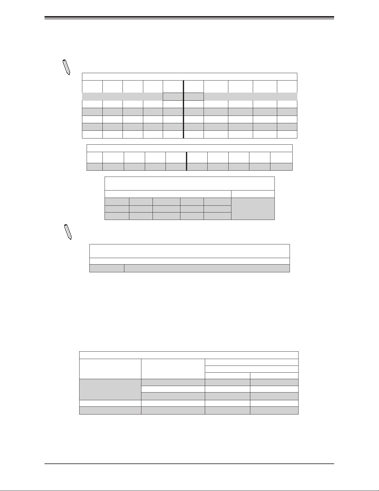
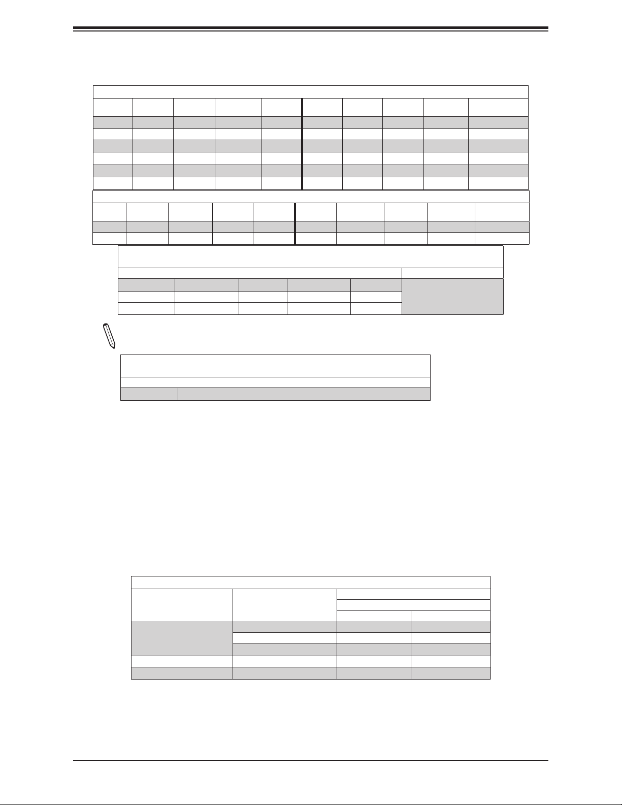
DCPMM Population Table for the X11UP Motherboards (w/8 DIMM slots)
Note: The following tables are supported by the X11SPL-F only.
Symmetric Population within CPU Socket
Modes DIMMC1 DIMMB1 DIMMA1 DIMMA2 DIMMD2 DIMMD1 DIMME1 DIMMF1
AD DRAM1 DRAM1 DRAM1 DCPMM DCPMM DRAM1 DRAM1 DRAM1 2-1-1
MM DRAM2 DRAM2 DRAM2 DCPMM DCPMM DRAM2 DRAM2 DRAM2 2-1-1
AD + MM DRAM3 DRAM3 DRAM3 DCPMM DCPMM DRAM3 DRAM3 DRAM3 2-1-1
AD DCPMM DRAM1 DRAM1 DRAM1 DRAM1 DCPMM 1-1-1
MM DCPMM DRAM1 DRAM1 DRAM1 DRAM1 DCPMM 1-1-1
AD + MM DCPMM DRAM3 DRAM3 DRAM3 DRAM3 DCPMM 1-1-1
Asymmetric Population within CPU Socket
Modes DIMMC1 DIMMB1 DIMMA1 DIMMA2 DIMMD2 DIMMD1 DIMME1 DIMMF1
AD DRAM1 DRAM1 DRAM1 DCPMM DRAM1 DRAM1 DRAM1 2-1-1
Channel
Cong.
Channel
Cong.
(for the two tables above)
Legend
DDR4 Type Capacity
DRAM1 RDIMM 3DS RDIMM LRDIMM 3DS LRDIMM
DRAM2 RDIMM - -
DRAM3 RDIMM 3DS RDIMM LRDIMM -
Refer to Validation
Matrix (DDR4 DIMMs
validated with DCPMM)
below.
Note: DDR4 single rank x8 is not available for DCPMM Memory Mode or App-Direct
Mode.
(forthersttwotables above)
DCPMM Any Capacity (Uniformly for all channels for a given conguration)
Legend
Capacity
• For each individual population, rearrangements between channels are allowed as long as the resulting population is
compliant with the Supermicro X11OPx/X11QPx/X11DPx/X11SPx memory population rules for the 2nd Gen Intel Xeon
Scalable-SP (82xx/62xx/52xx/4215 series) processors.
• For each individual population, please use the same DDR4 DIMM in all slots.
• For each individual population, sockets are normally symmetric with exceptions for 1 DCPMM per socket and 1 DCPMM
per node case. Currently, DCPMM modules operate at 2666 MHz.
• No mixing of DCPMM and NVMDIMMs within the same platform is allowed.
• This DCPMM population guide targets a balanced DCPMM-to-DRAM-cache ratio in MM and MM + AD modes.
Validation Matrix (DDR4 DIMMs Validated w/DCPMM)
DIMM Type
RDIMM
LRDIMM 4Rx4 N/A 64GB
LRDIMM 3DS 8Rx4 (4H) N/A 128GB
Ranks Per DIMM
& Data Width
(Stack)
1Rx4 8GB 16GB
2Rx8 8GB 16GB
2Rx4 16GB 32GB
DIMM Capacity (GB)
DRAM Density
4Gb 8Gb
14
Page 15
Chapter 2: DCPMM Memory Installation
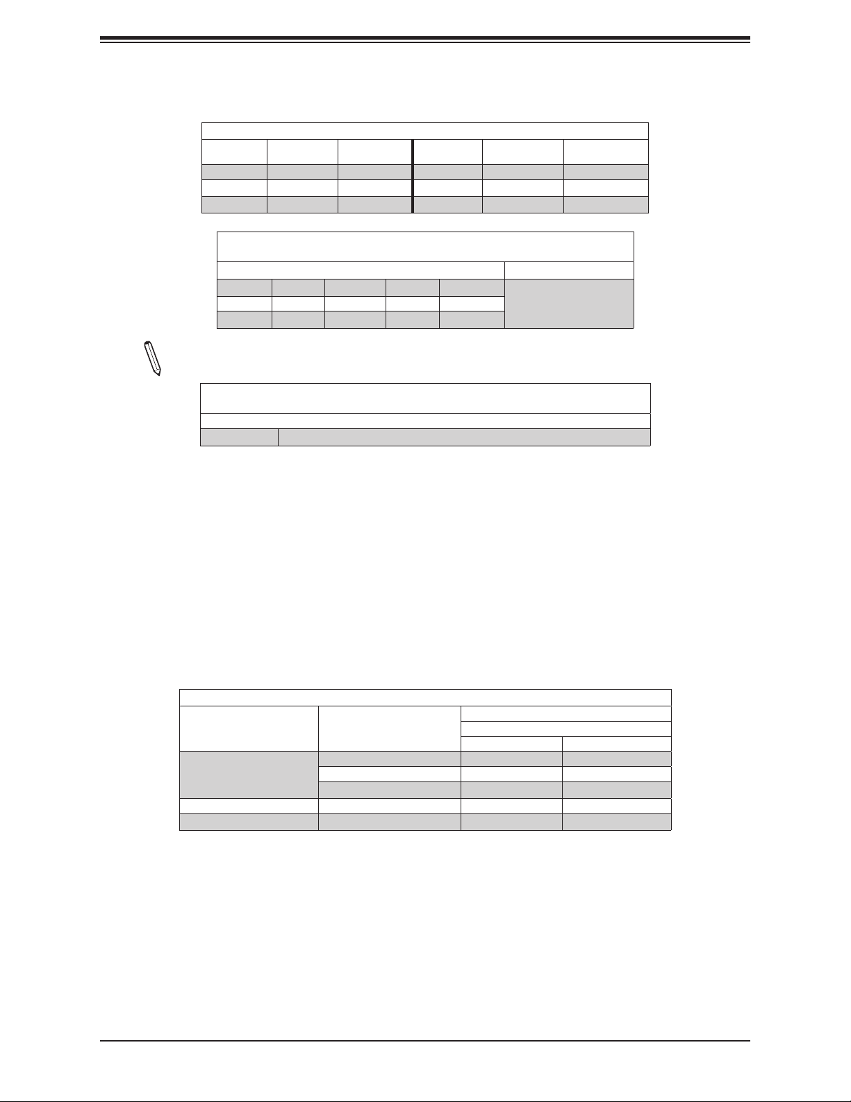
DCPMM Population Table for the X11DP Motherboards (w/8 DIMM Slots)
Symmetric Population within 1 CPU socket
Modes
AD DCPMM DRAM1 DRAM1 DCPMM 1-1
MM DCPMM DRAM1 DRAM1 DCPMM 1-1
AD + MM DCPMM DRAM3 DRAM3 DCPMM 1-1
DRAM1 RDIMM 3DS RDIMM LRDIMM 3DS LRDIMM
DRAM2 RDIMM - -
DRAM3 RDIMM 3DS RDIMM LRDIMM -
P1-
DIMME1
Note: DDR4 single rank x8 is not available for DCPMM Memory Mode or App-Direct
Mode.
P1-
DIMMD1
P1-
DIMMA1
P1-
DIMMB1
ChannelCong.
Legend
(for the table above)
DDR4 Type Capacity
Refer to Validation Matrix
(DDR4 DIMMs validated with
DCPMM) below.
(forthersttableabove)
Legend
Capacity
DCPMM Any Capacity (Uniformly for all channels for a given conguration)
• Mode denitions: AD=App Direct Mode, MM=Memory Mode, AD+MM=Mixed Mode
• For MM, general DDR4+DCPMM ratio is between 1:4 and 1:16. Excessive capacity for DCPMM can be used for AD.
• For each individual population, rearrangements between channels are allowed as long as the resulting population is
compliant with the Supermicro X11OPx/X11QPx/X11DPx/X11SPx memory population rules for the 2nd Gen Intel Xeon
Scalable-SP (82xx/62xx/52xx/4215 series) processors.
• For each individual population, please use the same DDR4 DIMM in all slots.
• For each individual population, sockets are normally symmetric with exceptions for 1 DCPMM per socket and 1 DCPMM
per node case. Currently, DCPMM modules operate at 2666 MHz.
• No mixing of DCPMM and NVMDIMMs within the same platform is allowed.
• This DCPMM population guide targets a balanced DCPMM-to-DRAM-cache ratio in MM and MM + AD modes.
Validation Matrix (DDR4 DIMMs Validated w/DCPMM)
DIMM Type
RDIMM
LRDIMM 4Rx4 N/A 64GB
LRDIMM 3DS 8Rx4 (4H) N/A 128GB
Ranks Per DIMM
& Data Width
(Stack)
1Rx4 8GB 16GB
2Rx8 8GB 16GB
2Rx4 16GB 32GB
DIMM Capacity (GB)
DRAM Density
4Gb 8Gb
15
Page 16
Super 1st Gen. DCPMM Memory for X11OPx/X11QPx/X11DPx/X11SPx Motherboards Guide
DCPMM Population Table for the X11DP Motherboards (w/12 DIMM Slots)
Symmetric Population within 1 CPU Socket
Modes
AD DCPMM DRAM1 DRAM1 DRAM1 DRAM1 DCPMM 1-1-1
MM DCPMM DRAM1 DRAM1 DRAM1 DRAM1 DCPMM 1-1-1
AD + MM DCPMM DRAM3 DRAM3 DRAM3 DRAM3 DCPMM 1-1-1
P1-
DIMMF1
DRAM1 RDIMM 3DS RDIMM LRDIMM 3DS LRDIMM
DRAM2 RDIMM - -
DRAM3 RDIMM 3DS RDIMM LRDIMM -
Note: DDR4 single rank x8 is not available for DCPMM Memory Mode or App-Direct
Mode.
P1-
DIMME1
P1-
DIMMD1
P1-
DIMMA1
P1-
DIMMB1
P1-
DIMMC1
Legend
(for the table above)
DDR4 Type Capacity
Refer to Validation Matrix
(DDR4 DIMMs validated with
DCPMM) below.
ChannelCong.
(forthersttableabove)
Legend
Capacity
DCPMM Any Capacity (Uniformly for all channels for a given conguration)
• * 2nd socket has no DCPMM DIMM
• Mode denitions: AD=App Direct Mode, MM=Memory Mode, AD+MM=Mixed Mode
• For MM, general DDR4+DCPMM ratio is between 1:4 and 1:16. Excessive capacity for DCPMM can be used for AD.
• For each individual population, rearrangements between channels are allowed as long as the resulting population is
compliant with the Supermicro X11OPx/X11QPx/X11DPx/X11SPx memory population rules for the 2nd Gen Intel Xeon
Scalable-SP (82xx/62xx/52xx/4215 series) processors.
• For each individual population, please use the same DDR4 DIMM in all slots.
• For each individual population, sockets are normally symmetric with exceptions for 1 DCPMM per socket and 1 DCPMM
per node case. Currently, DCPMM modules operate at 2666 MHz.
• No mixing of DCPMM and NVMDIMMs within the same platform is allowed.
• This DCPMM population guide targets a balanced DCPMM-to-DRAM-cache ratio in MM and MM + AD modes.
Validation Matrix (DDR4 DIMMs Validated w/DCPMM)
DIMM Type
RDIMM
LRDIMM 4Rx4 N/A 64GB
LRDIMM 3DS 8Rx4 (4H) N/A 128GB
Ranks Per DIMM
& Data Width
(Stack)
1Rx4 8GB 16GB
2Rx8 8GB 16GB
2Rx4 16GB 32GB
DIMM Capacity (GB)
DRAM Density
4Gb 8Gb
16
Page 17
Chapter 2: DCPMM Memory Installation
DCPMM Population Table for the X11DP Motherboards (w/16 DIMM Slots)
Symmetric Population within 1 CPU Socket
Modes
AD DRAM1 DRAM1 DRAM1 DCPMM DCPMM DRAM1 DRAM1 DRAM1 2-1-1
MM DRAM2 DRAM2 DRAM2 DCPMM DCPMM DRAM2 DRAM2 DRAM2 2-1-1
AD + MM DRAM3 DRAM3 DRAM3 DCPMM DCPMM DRAM3 DRAM3 DRAM3 2-1-1
AD DCPMM DRAM1 DRAM1 - - DRAM1 DRAM1 DCPMM 1-1-1
MM DCPMM DRAM1 DRAM1 - - DRAM1 DRAM1 DCPMM 1-1-1
AD + MM DCPMM DRAM3 DRAM3 - - DRAM3 DRAM3 DCPMM 1-1-1
Modes
AD DRAM1 DRAM1 DRAM1 - DCPMM DRAM1 DRAM1 DRAM1 2-1-1
AD* DRAM1 DRAM1 DRAM1 - DCPMM DRAM1 DRAM1 DRAM1 2-1-1
P1-
DIMMF1
P1-
DIMMF1
DRAM1 RDIMM 3DS RDIMM LRDIMM 3DS LRDIMM
DRAM2 RDIMM - - -
DRAM3 RDIMM 3DS RDIMM LRDIMM -
P1-
DIMME1
P1-
DIMME1
P1-
DIMMD1
P1-
DIMMD2
P1-
DIMMA2
P1-
DIMMA1
P1-
DIMMB1
Asymmetric Population within 1 CPU Socket
P1-
DIMMD1
P1-
DIMMD2
P1-
DIMMA2
P1-
DIMMA1
P1-
DIMMB1
Legend
(for the two tables above)
DDR4 Type Capacity
Refer to Validation Matrix (DDR4
P1-
DIMMC1
DIMMC1
DIMMs validated with DCPMM)
below.
P1-
ChannelCong.
ChannelCong.
Note: DDR4 single rank x8 is not available for DCPMM Memory Mode or App-Direct
Mode.
(forthersttwotables above)
DCPMM Any Capacity (Uniformly for all channels for a given conguration)
Legend
Capacity
• * 2nd socket has no DCPMM DIMM
• Mode denitions: AD=App Direct Mode, MM=Memory Mode, AD+MM=Mixed Mode
• For MM, general DDR4+DCPMM ratio is between 1:4 and 1:16. Excessive capacity for DCPMM can be used for AD.
• For each individual population, rearrangements between channels are allowed as long as the resulting population is
compliant with the Supermicro X11OPx/X11QPx/X11DPx/X11SPx memory population rules for the 2nd Gen Intel Xeon
Scalable-SP (82xx/62xx/52xx/4215 series) processors.
• For each individual population, please use the same DDR4 DIMM in all slots.
• For each individual population, sockets are normally symmetric with exceptions for 1 DCPMM per socket and 1 DCPMM
per node case. Currently, DCPMM modules operate at 2666 MHz.
• No mixing of DCPMM and NVMDIMMs within the same platform is allowed.
• This DCPMM population guide targets a balanced DCPMM-to-DRAM-cache ratio in MM and MM + AD modes.
Validation Matrix (DDR4 DIMMs Validated w/DCPMM)
DIMM Type
RDIMM
LRDIMM 4Rx4 N/A 64GB
LRDIMM 3DS 8Rx4 (4H) N/A 128GB
Ranks Per DIMM
& Data Width
(Stack)
1Rx4 8GB 16GB
2Rx8 8GB 16GB
2Rx4 16GB 32GB
DIMM Capacity (GB)
DRAM Density
4Gb 8Gb
17
Page 18

Super 1st Gen. DCPMM Memory for X11OPx/X11QPx/X11DPx/X11SPx Motherboards Guide
DCPMM Population Table for the X11DP Motherboards (w/24 DIMM Slots)
Symmetric Population within 1 CPU Socket
Modes
AD DRAM1 DCPMM DRAM1 DCPMM DRAM1 DCPMM DCPMM DRAM1 DCPMM DRAM1 DCPMM DRAM1 2-2-2
MM DRAM1 DCPMM DRAM1 DCPMM DRAM1 DCPMM DCPMM DRAM1 DCPMM DRAM1 DCPMM DRAM1 2-2-2
AD + MM DRAM3 DCPMM DRAM3 DCPMM DRAM3 DCPMM DCPMM DRAM3 DCPMM DRAM3 DCPMM DRAM3 2-2-2
AD DRAM1 - DRAM1 - DRAM1 DCPMM DCPMM DRAM1 - DRAM1 - DRAM1 2-1-1
MM DRAM2 - DRAM2 - DRAM2 DCPMM DCPMM DRAM2 - DRAM2 - DRAM2 2-1-1
AD + MM DRAM3 - DRAM3 - DRAM3 DCPMM DCPMM DRAM3 - DRAM3 - DRAM3 2-1-1
AD DRAM1 - DRAM1 DCPMM DRAM1 DCPMM DCPMM DRAM1 DCPMM DRAM1 - DRAM1 2-2-1
MM DRAM1 - DRAM1 DCPMM DRAM1 DCPMM DCPMM DRAM1 DCPMM DRAM1 - DRAM1 2-2-1
AD + MM DRAM3 - DRAM3 DCPMM DRAM3 DCPMM DCPMM DRAM3 DCPMM DRAM3 - DRAM3 2-2-1
AD DCPMM - DRAM1 - DRAM1 - - DRAM1 - DRAM1 - DCPMM 1-1-1
MM DCPMM - DRAM1 - DRAM1 - - DRAM1 - DRAM1 - DCPMM 1-1-1
AD + MM DCPMM - DRAM3 - DRAM3 - - DRAM3 - DRAM3 - DCPMM 1-1-1
AD DCPMM - DRAM1 DRAM1 DRAM1 DRAM1 DRAM1 DRAM1 DRAM1 DRAM1 - DCPMM 2-2-1
Modes
AD DRAM1 - DRAM1 - DRAM1 - DCPMM DRAM1 - DRAM1 - DRAM1 2/1-1-1
AD* DRAM1 - DRAM1 - DRAM1 - DCPMM DRAM1 - DRAM1 - DRAM1 2/1-1-1
P1-
DIMMF1
P1-
DIMMF1
P1-
DIMMF2
P1-
DIMMF2
P1-
DIMME1
P1-
DIMME1
P1-
DIMME2
P1-
DIMMD1
P1-
DIMMD2
P1-
DIMMA2
DIMMA1
Asymmetric Population within 1 CPU Socket
P1-
DIMME2
P1-
DIMMD1
P1-
DIMMD2
P1-
DIMMA2
P1-
DIMMA1
P1-
P1-
DIMMB2
P1-
DIMMB2
P1-
DIMMB1
P1-
DIMMB1
P1-
DIMMC2
P1-
DIMMC2
P1-
DIMMC1
P1-
DIMMC1
Channel
Cong.
Channel
Cong.
Legend (for the two tables above)
DDR4 Type Capacity
DRAM1 RDIMM 3DS RDIMM LRDIMM 3DS LRDIMM
DRAM2 RDIMM - -
DRAM3 RDIMM 3DS RDIMM LRDIMM -
Refer to Validation Matrix
(DDR4 DIMMs validated with
DCPMM) below.
Note: DDR4 single rank x8 is not available for DCPMM Memory Mode or App-Direct
Mode.
Legend(forthersttwo tablesabove)
Capacity
DCPMM Any Capacity (Uniformly for all channels for a given conguration)
• * 2nd socket has no DCPMM DIMM
• Mode denitions: AD=App Direct Mode, MM=Memory Mode, AD+MM=Mixed Mode
• For MM, general DDR4+DCPMM ratio is between 1:4 and 1:16. Excessive capacity for DCPMM can be used for AD.
• For each individual population, rearrangements between channels are allowed as long as the resulting population is
compliant with the Supermicro X11OPx/X11QPx/X11DPx/X11SPx memory population rules for the 2nd Gen Intel Xeon
Scalable-SP (82xx/62xx/52xx/4215 series) processors.
• For each individual population, please use the same DDR4 DIMM in all slots.
• For each individual population, sockets are normally symmetric with exceptions for 1 DCPMM per socket and 1 DCPMM
per node case. Currently, DCPMM modules operate at 2666 MHz.
• No mixing of DCPMM and NVMDIMMs within the same platform is allowed.
• This DCPMM population guide targets a balanced DCPMM-to-DRAM-cache ratio in MM and MM + AD modes.
Validation Matrix (DDR4 DIMMs Validated w/DCPMM)
DIMM Type
RDIMM
LRDIMM 4Rx4 N/A 64GB
LRDIMM 3DS 8Rx4 (4H) N/A 128GB
Ranks Per DIMM
& Data Width
(Stack)
1Rx4 8GB 16GB
2Rx8 8GB 16GB
2Rx4 16GB 32GB
DIMM Capacity (GB)
DRAM Density
4Gb 8Gb
18
Page 19

Chapter 2: DCPMM Memory Installation
DCPMM Population Table for the X11QP Motherboards (w/48 DIMM Slots)
Symmetric Population
2-2-2 (ForChannelConguration:2-2-2)
Modes
CPU1
AD DRAM1 DCPMM DRAM1 DCPMM DRAM1 DCPMM DCPMM DRAM1 DCPMM DRAM1 DCPMM DRAM1
MM DRAM1 DCPMM DRAM1 DCPMM DRAM1 DCPMM DCPMM DRAM1 DCPMM DRAM1 DCPMM DRAM1
AD + MM DRAM3 DCPMM DRAM3 DCPMM DRAM3 DCPMM DCPMM DRAM3 DCPMM DRAM3 DCPMM DRAM3
CPU2
AD DRAM1 DCPMM DRAM1 DCPMM DRAM1 DCPMM DCPMM DRAM1 DCPMM DRAM1 DCPMM DRAM1
MM DRAM1 DCPMM DRAM1 DCPMM DRAM1 DCPMM DCPMM DRAM1 DCPMM DRAM1 DCPMM DRAM1
AD + MM DRAM3 DCPMM DRAM3 DCPMM DRAM3 DCPMM DCPMM DRAM3 DCPMM DRAM3 DCPMM DRAM3
CPU3
AD DRAM1 DCPMM DRAM1 DCPMM DRAM1 DCPMM DCPMM DRAM1 DCPMM DRAM1 DCPMM DRAM1
MM DRAM1 DCPMM DRAM1 DCPMM DRAM1 DCPMM DCPMM DRAM1 DCPMM DRAM1 DCPMM DRAM1
AD + MM DRAM3 DCPMM DRAM3 DCPMM DRAM3 DCPMM DCPMM DRAM3 DCPMM DRAM3 DCPMM DRAM3
CPU4
AD DRAM1 DCPMM DRAM1 DCPMM DRAM1 DCPMM DCPMM DRAM1 DCPMM DRAM1 DCPMM DRAM1
MM DRAM1 DCPMM DRAM1 DCPMM DRAM1 DCPMM DCPMM DRAM1 DCPMM DRAM1 DCPMM DRAM1
AD + MM DRAM3 DCPMM DRAM3 DCPMM DRAM3 DCPMM DCPMM DRAM3 DCPMM DRAM3 DCPMM DRAM3
P1-
DIMMF1
P2-
DIMMF1
P3-
DIMMF1
P4-
DIMMF1
P1-
DIMMF2
P2-
DIMMF2
P3-
DIMMF2
P4-
DIMMF2
P1-
DIMME1
P2-
DIMME1
P3-
DIMME1
P4-
DIMME1
P1-
DIMME2
P2-
DIMME2
P3-
DIMME2
P4-
DIMME2
P1-
DIMMD1
P2-
DIMMD1
P3-
DIMMD1
P4-
DIMMD1
P1-
DIMMD2
P2-
DIMMD2
P3-
DIMMD2
P4-
DIMMD2
P1-
DIMMA2
P2-
DIMMA2
P3-
DIMMA2
P4-
DIMMA2
P1-
DIMMA1
P2-
DIMMA1
P3-
DIMMA1
P4-
DIMMA1
P1-
DIMMB2
P2-
DIMMB2
P3-
DIMMB2
P4-
DIMMB2
P1-
DIMMB1
P2-
DIMMB1
P3-
DIMMB1
P4-
DIMMB1
P1-
DIMMC2
P2-
DIMMC2
P3-
DIMMC2
P4-
DIMMC2
P1-
DIMMC1
P2-
DIMMC1
P3-
DIMMC1
P4-
DIMMC1
Note: To be continued on the next page.
19
Page 20

Super 1st Gen. DCPMM Memory for X11OPx/X11QPx/X11DPx/X11SPx Motherboards Guide
DCPMM Population Table for the X11QP Motherboards (w/48 DIMM Slots)
Symmetric Population
2-1-1 (ForChannelConguration:2-1-1)
Modes
CPU1
AD DRAM1 - DRAM1 - DRAM1 DCPMM DCPMM DRAM1 - DRAM1 - DRAM1
MM DRAM2 - DRAM2 - DRAM2 DCPMM DCPMM DRAM2 - DRAM2 - DRAM2
AD + MM DRAM3 - DRAM3 - DRAM3 DCPMM DCPMM DRAM3 - DRAM3 - DRAM3
CPU2
AD DRAM1 - DRAM1 - DRAM1 DCPMM DCPMM DRAM1 - DRAM1 - DRAM1
MM DRAM2 - DRAM2 - DRAM2 DCPMM DCPMM DRAM2 - DRAM2 - DRAM2
AD + MM DRAM3 - DRAM3 - DRAM3 DCPMM DCPMM DRAM3 - DRAM3 - DRAM3
CPU3
AD DRAM1 - DRAM1 - DRAM1 DCPMM DCPMM DRAM1 - DRAM1 - DRAM1
MM DRAM2 - DRAM2 - DRAM2 DCPMM DCPMM DRAM2 - DRAM2 - DRAM2
AD + MM DRAM3 - DRAM3 - DRAM3 DCPMM DCPMM DRAM3 - DRAM3 - DRAM3
CPU4
AD DRAM1 - DRAM1 - DRAM1 DCPMM DCPMM DRAM1 - DRAM1 - DRAM1
MM DRAM2 - DRAM2 - DRAM2 DCPMM DCPMM DRAM2 - DRAM2 - DRAM2
AD + MM DRAM3 - DRAM3 - DRAM3 DCPMM DCPMM DRAM3 - DRAM3 - DRAM3
P1-
DIMMF1
P2-
DIMMF1
P3-
DIMMF1
P4-
DIMMF1
P1-
DIMMF2
P2-
DIMMF2
P3-
DIMMF2
P4-
DIMMF2
P1-
DIMME1
P2-
DIMME1
P3-
DIMME1
P4-
DIMME1
P1-
DIMME2
P2-
DIMME2
P3-
DIMME2
P4-
DIMME2
P1-
DIMMD1
P2-
DIMMD1
P3-
DIMMD1
P4-
DIMMD1
P1-
DIMMD2
P2-
DIMMD2
P3-
DIMMD2
P4-
DIMMD2
P1-
DIMMA2
P2-
DIMMA2
P3-
DIMMA2
P4-
DIMMA2
P1-
DIMMA1
P2-
DIMMA1
P3-
DIMMA1
P4-
DIMMA1
P1-
DIMMB2
P2-
DIMMB2
P3-
DIMMB2
P4-
DIMMB2
P1-
DIMMB1
P2-
DIMMB1
P3-
DIMMB1
P4-
DIMMB1
P1-
DIMMC2
P2-
DIMMC2
P3-
DIMMC2
P4-
DIMMC2
P1-
DIMMC1
P2-
DIMMC1
P3-
DIMMC1
P4-
DIMMC1
Symmetric Population
2-2-1 (ForChannelConguration:2-2-1)
Modes
CPU1
AD DRAM1 - DRAM1 DCPMM DRAM1 DCPMM DCPMM DRAM1 DCPMM DRAM1 - DRAM1
MM DRAM1 - DRAM1 DCPMM DRAM1 DCPMM DCPMM DRAM1 DCPMM DRAM1 - DRAM1
AD + MM DRAM3 - DRAM3 DCPMM DRAM3 DCPMM DCPMM DRAM3 DCPMM DRAM3 - DRAM3
AD DCPMM - DRAM1 DRAM1 DRAM1 DRAM1 DRAM1 DRAM1 DRAM1 DRAM1 - DCPMM 2-2-1
CPU2
AD DRAM1 - DRAM1 DCPMM DRAM1 DCPMM DCPMM DRAM1 DCPMM DRAM1 - DRAM1
MM DRAM1 - DRAM1 DCPMM DRAM1 DCPMM DCPMM DRAM1 DCPMM DRAM1 - DRAM1
AD + MM DRAM3 - DRAM3 DCPMM DRAM3 DCPMM DCPMM DRAM3 DCPMM DRAM3 - DRAM3
AD DCPMM - DRAM1 DRAM1 DRAM1 DRAM1 DRAM1 DRAM1 DRAM1 DRAM1 - DCPMM 2-2-1
CPU3
AD DRAM1 - DRAM1 DCPMM DRAM1 DCPMM DCPMM DRAM1 DCPMM DRAM1 - DRAM1
MM DRAM1 - DRAM1 DCPMM DRAM1 DCPMM DCPMM DRAM1 DCPMM DRAM1 - DRAM1
AD + MM DRAM3 - DRAM3 DCPMM DRAM3 DCPMM DCPMM DRAM3 DCPMM DRAM3 - DRAM3
AD DCPMM - DRAM1 DRAM1 DRAM1 DRAM1 DRAM1 DRAM1 DRAM1 DRAM1 - DCPMM 2-2-1
CPU4
AD DRAM1 - DRAM1 DCPMM DRAM1 DCPMM DCPMM DRAM1 DCPMM DRAM1 - DRAM1
MM DRAM1 - DRAM1 DCPMM DRAM1 DCPMM DCPMM DRAM1 DCPMM DRAM1 - DRAM1
AD + MM DRAM3 - DRAM3 DCPMM DRAM3 DCPMM DCPMM DRAM3 DCPMM DRAM3 - DRAM3
AD DCPMM - DRAM1 DRAM1 DRAM1 DRAM1 DRAM1 DRAM1 DRAM1 DRAM1 - DCPMM 2-2-1
P1-
DIMMF1
P2-
DIMMF1
P3-
DIMMF1
P4-
DIMMF1
P1-
DIMMF2
P2-
DIMMF2
P3-
DIMMF2
P4-
DIMMF2
P1-
DIMME1
P2-
DIMME1
P3-
DIMME1
P4-
DIMME1
P1-
DIMME2
P2-
DIMME2
P3-
DIMME2
P4-
DIMME2
P1-
DIMMD1
P2-
DIMMD1
P3-
DIMMD1
P4-
DIMMD1
P1-
DIMMD2
P2-
DIMMD2
P3-
DIMMD2
P4-
DIMMD2
P1-
DIMMA2
P2-
DIMMA2
P3-
DIMMA2
P4-
DIMMA2
P1-
DIMMA1
P2-
DIMMA1
P3-
DIMMA1
P4-
DIMMA1
P1-
DIMMB2
P2-
DIMMB2
P3-
DIMMB2
P4-
DIMMB2
P1-
DIMMB1
P2-
DIMMB1
P3-
DIMMB1
P4-
DIMMB1
P1-
DIMMC2
P2-
DIMMC2
P3-
DIMMC2
P4-
DIMMC2
P1-
DIMMC1
P2-
DIMMC1
P3-
DIMMC1
P4-
DIMMC1
Note: To be continued on the next page.
20
Page 21

Chapter 2: DCPMM Memory Installation
DCPMM Population Table for the X11QP Motherboards (w/48 DIMM Slots)
Symmetric Population
1-1-1 (ForChannelConguration:1-1-1)
Modes
CPU1
AD DCPMM - DRAM1 - DRAM1 - - DRAM1 - DRAM1 - DCPMM
MM DCPMM - DRAM1 - DRAM1 - - DRAM1 - DRAM1 - DCPMM
AD + MM DCPMM - DRAM3 - DRAM3 - - DRAM3 - DRAM3 - DCPMM
CPU2
AD DCPMM - DRAM1 - DRAM1 - - DRAM1 - DRAM1 - DCPMM
MM DCPMM - DRAM1 - DRAM1 - - DRAM1 - DRAM1 - DCPMM
AD + MM DCPMM - DRAM3 - DRAM3 - - DRAM3 - DRAM3 - DCPMM
CPU3
AD DCPMM - DRAM1 - DRAM1 - - DRAM1 - DRAM1 - DCPMM
MM DCPMM - DRAM1 - DRAM1 - - DRAM1 - DRAM1 - DCPMM
AD + MM DCPMM - DRAM3 - DRAM3 - - DRAM3 - DRAM3 - DCPMM
CPU4
AD DCPMM - DRAM1 - DRAM1 - - DRAM1 - DRAM1 - DCPMM
MM DCPMM - DRAM1 - DRAM1 - - DRAM1 - DRAM1 - DCPMM
AD + MM DCPMM - DRAM3 - DRAM3 - - DRAM3 - DRAM3 - DCPMM
2/1-1-1 (ForChannelConguration:2/1-1-1)
Modes
CPU1
AD DRAM1 - DRAM1 - DRAM1 - DCPMM DRAM1 - DRAM1 - DRAM1
CPU2
AD DRAM1 - DRAM1 - DRAM1 - DCPMM DRAM1 - DRAM1 - DRAM1
CPU3
AD DRAM1 - DRAM1 - DRAM1 - DCPMM DRAM1 - DRAM1 - DRAM1
CPU4
AD DRAM1 - DRAM1 - DRAM1 - DCPMM DRAM1 - DRAM1 - DRAM1
P1-
DIMMF1
P2-
DIMMF1
P3-
DIMMF1
P4-
DIMMF1
P1-
DIMMF1
P2-
DIMMF1
P3-
DIMMF1
P4-
DIMMF1
P1-
DIMMF2
P2-
DIMMF2
P3-
DIMMF2
P4-
DIMMF2
P1-
DIMME1
P2-
DIMME1
P3-
DIMME1
P4-
DIMME1
P1-
DIMME2
P2-
DIMME2
P3-
DIMME2
P4-
DIMME2
P1-
DIMMD1
P2-
DIMMD1
P3-
DIMMD1
P4-
DIMMD1
P1-
DIMMD2
P2-
DIMMD2
P3-
DIMMD2
P4-
DIMMD2
Asymmetric Population
P1-
DIMMF2
P2-
DIMMF2
P3-
DIMMF2
P4-
DIMMF2
P1-
DIMME1
P2-
DIMME1
P3-
DIMME1
P4-
DIMME1
P1-
DIMME2
P2-
DIMME2
P3-
DIMME2
P4-
DIMME2
P1-
DIMMD1
P2-
DIMMD1
P3-
DIMMD1
P4-
DIMMD1
P1-
DIMMD2
P2-
DIMMD2
P3-
DIMMD2
P4-
DIMMD2
Legend(forthevetables above)
DDR4 Type Capacity
DRAM1 RDIMM 3DS RDIMM LRDIMM 3DS LRDIMM
DRAM2 RDIMM - -
DRAM3 RDIMM 3DS RDIMM LRDIMM -
P1-
DIMMA2
P2-
DIMMA2
P3-
DIMMA2
P4-
DIMMA2
P1-
DIMMA2
P2-
DIMMA2
P3-
DIMMA2
P4-
DIMMA2
P1-
DIMMA1
P2-
DIMMA1
P3-
DIMMA1
P4-
DIMMA1
P1-
DIMMA1
P2-
DIMMA1
P3-
DIMMA1
P4-
DIMMA1
P1-
DIMMB2
P2-
DIMMB2
P3-
DIMMB2
P4-
DIMMB2
P1-
DIMMB2
P2-
DIMMB2
P3-
DIMMB2
P4-
DIMMB2
Refer to Validation Matrix
(DDR4 DIMMs validated with
DCPMM) on the next page.
P1-
DIMMB1
P2-
DIMMB1
P3-
DIMMB1
P4-
DIMMB1
P1-
DIMMB1
P2-
DIMMB1
P3-
DIMMB1
P4-
DIMMB1
P1-
DIMMC2
P2-
DIMMC2
P3-
DIMMC2
P4-
DIMMC2
P1-
DIMMC2
P2-
DIMMC2
P3-
DIMMC2
P4-
DIMMC2
P1-
DIMMC1
P2-
DIMMC1
P3-
DIMMC1
P4-
DIMMC1
P1-
DIMMC1
P2-
DIMMC1
P3-
DIMMC1
P4-
DIMMC1
Note: DDR4 single rank x8 is not available for DCPMM Memory Mode or App-Direct
Mode.
Note: To be continued on the next page.
21
Page 22

Super 1st Gen. DCPMM Memory for X11OPx/X11QPx/X11DPx/X11SPx Motherboards Guide
DCPMM Population Table for the X11QP Motherboards (w/48 Slots)
Legend(fortherstve tablesabove)
Capacity
DCPMM Any Capacity (Uniformly for all channels for a given conguration)
• Mode denitions: AD=App Direct Mode, MM=Memory Mode, AD+MM=Mixed Mode
• For MM, general DDR4+DCPMM ratio is between 1:4 and 1:16. Excessive capacity for DCPMM can be used for AD.
For each individual population, rearrangements between channels are allowed as long as the resulting population is
compliant with the Supermicro X11OPx/X11QPx/X11DPx/X11SPx memory population rules for the 2nd Gen Intel Xeon
Scalable-SP (82xx/62xx/52xx/4215 series) processors.
• For each individual population, please use the same DDR4 DIMM in all slots.
• For each individual population, sockets are normally symmetric with exceptions for 1 DCPMM per socket and 1 DCPMM
per node case. No mixing of DCPMM and NVMDIMMs within the same platform is allowed.
• This DCPMM population guide targets a balanced DCPMM-to-DRAM-cache ratio in MM and MM + AD modes.
Validation Matrix (DDR4 DIMMs Validated w/DCPMM)
DIMM Type
RDIMM
LRDIMM 4Rx4 N/A 64GB
LRDIMM 3DS 8Rx4 (4H) N/A 128GB
Ranks Per DIMM
& Data Width
(Stack)
1Rx4 8GB 16GB
2Rx8 8GB 16GB
2Rx4 16GB 32GB
DIMM Capacity (GB)
DRAM Density
4Gb 8Gb
22
Page 23

Chapter 2: DCPMM Memory Installation
DCPMM Population Table for the X11OP Motherboards (w/96 DIMM Slots)
Symmetric Population
2-2-2 (ForChannelConguration:2-2-2)
Modes
CPU1
AD DRAM1 DCPMM DRAM1 DCPMM DRAM1 DCPMM DCPMM DRAM1 DCPMM DRAM1 DCPMM DRAM1
MM DRAM1 DCPMM DRAM1 DCPMM DRAM1 DCPMM DCPMM DRAM1 DCPMM DRAM1 DCPMM DRAM1
AD + MM DRAM3 DCPMM DRAM3 DCPMM DRAM3 DCPMM DCPMM DRAM3 DCPMM DRAM3 DCPMM DRAM3
CPU2
AD DRAM1 DCPMM DRAM1 DCPMM DRAM1 DCPMM DCPMM DRAM1 DCPMM DRAM1 DCPMM DRAM1
MM DRAM1 DCPMM DRAM1 DCPMM DRAM1 DCPMM DCPMM DRAM1 DCPMM DRAM1 DCPMM DRAM1
AD + MM DRAM3 DCPMM DRAM3 DCPMM DRAM3 DCPMM DCPMM DRAM3 DCPMM DRAM3 DCPMM DRAM3
CPU3
AD DRAM1 DCPMM DRAM1 DCPMM DRAM1 DCPMM DCPMM DRAM1 DCPMM DRAM1 DCPMM DRAM1
MM DRAM1 DCPMM DRAM1 DCPMM DRAM1 DCPMM DCPMM DRAM1 DCPMM DRAM1 DCPMM DRAM1
AD + MM DRAM3 DCPMM DRAM3 DCPMM DRAM3 DCPMM DCPMM DRAM3 DCPMM DRAM3 DCPMM DRAM3
CPU4
AD DRAM1 DCPMM DRAM1 DCPMM DRAM1 DCPMM DCPMM DRAM1 DCPMM DRAM1 DCPMM DRAM1
MM DRAM1 DCPMM DRAM1 DCPMM DRAM1 DCPMM DCPMM DRAM1 DCPMM DRAM1 DCPMM DRAM1
AD + MM DRAM3 DCPMM DRAM3 DCPMM DRAM3 DCPMM DCPMM DRAM3 DCPMM DRAM3 DCPMM DRAM3
CPU5
AD DRAM1 DCPMM DRAM1 DCPMM DRAM1 DCPMM DCPMM DRAM1 DCPMM DRAM1 DCPMM DRAM1
MM DRAM1 DCPMM DRAM1 DCPMM DRAM1 DCPMM DCPMM DRAM1 DCPMM DRAM1 DCPMM DRAM1
AD + MM DRAM3 DCPMM DRAM3 DCPMM DRAM3 DCPMM DCPMM DRAM3 DCPMM DRAM3 DCPMM DRAM3
CPU6
AD DRAM1 DCPMM DRAM1 DCPMM DRAM1 DCPMM DCPMM DRAM1 DCPMM DRAM1 DCPMM DRAM1
MM DRAM1 DCPMM DRAM1 DCPMM DRAM1 DCPMM DCPMM DRAM1 DCPMM DRAM1 DCPMM DRAM1
AD + MM DRAM3 DCPMM DRAM3 DCPMM DRAM3 DCPMM DCPMM DRAM3 DCPMM DRAM3 DCPMM DRAM3
CPU7
AD DRAM1 DCPMM DRAM1 DCPMM DRAM1 DCPMM DCPMM DRAM1 DCPMM DRAM1 DCPMM DRAM1
MM DRAM1 DCPMM DRAM1 DCPMM DRAM1 DCPMM DCPMM DRAM1 DCPMM DRAM1 DCPMM DRAM1
AD + MM DRAM3 DCPMM DRAM3 DCPMM DRAM3 DCPMM DCPMM DRAM3 DCPMM DRAM3 DCPMM DRAM3
CPU8
AD DRAM1 DCPMM DRAM1 DCPMM DRAM1 DCPMM DCPMM DRAM1 DCPMM DRAM1 DCPMM DRAM1
MM DRAM1 DCPMM DRAM1 DCPMM DRAM1 DCPMM DCPMM DRAM1 DCPMM DRAM1 DCPMM DRAM1
AD + MM DRAM3 DCPMM DRAM3 DCPMM DRAM3 DCPMM DCPMM DRAM3 DCPMM DRAM3 DCPMM DRAM3
P1-
DIMMF1
P2-
DIMMF1
P3-
DIMMF1
P4-
DIMMF1
P5-
DIMMF1
P6-
DIMMF1
P7-
DIMMF1
P8-
DIMMF1
P1-
DIMMF2
P2-
DIMMF2
P3-
DIMMF2
P4-
DIMMF2
P5-
DIMMF2
P6-
DIMMF2
P7-
DIMMF2
P8-
DIMMF2
P1-
DIMME1
P2-
DIMME1
P3-
DIMME1
P4-
DIMME1
P5-
DIMME1
P6-
DIMME1
P7-
DIMME1
P8-
DIMME1
P1-
DIMME2
P2-
DIMME2
P3-
DIMME2
P4-
DIMME2
P5-
DIMME2
P6-
DIMME2
P7-
DIMME2
P8-
DIMME2
P1-
DIMMD1
P2-
DIMMD1
P3-
DIMMD1
P4-
DIMMD1
P5-
DIMMD1
P6-
DIMMD1
P7-
DIMMD1
P8-
DIMMD1
P1-
DIMMD2
P2-
DIMMD2
P3-
DIMMD2
P4-
DIMMD2
P5-
DIMMD2
P6-
DIMMD2
P7-
DIMMD2
P8-
DIMMD2
P1-
DIMMA2
P2-
DIMMA2
P3-
DIMMA2
P4-
DIMMA2
P5-
DIMMA2
P6-
DIMMA2
P7-
DIMMA2
P8-
DIMMA2
P1-
DIMMA1
P2-
DIMMA1
P3-
DIMMA1
P4-
DIMMA1
P5-
IMMA1
P6-
DIMMA1
P7-
DIMMA1
P8-
DIMMA1
P1-
DIMMB2
P2-
DIMMB2
P3-
DIMMB2
P4-
DIMMB2
P5-
DIMMB2
P6-
DIMMB2
P7-
DIMMB2
P8-
DIMMB2
P1-
DIMMB1
P2-
DIMMB1
P3-
DIMMB1
P4-
DIMMB1
P5-
DIMMB1
P6-
DIMMB1
P7-
DIMMB1
P8-
DIMMB1
P1-
DIMMC2
P2-
DIMMC2
P3-
DIMMC2
P4-
DIMMC2
P5-
DIMMC2
P6-
DIMMC2
P7-
DIMMC2
P8-
DIMMC2
P1-
DIMMC1
P2-
DIMMC1
P3-
DIMMC1
P4-
DIMMC1
P5-
DIMMC1
P6-
DIMMC1
P7-
DIMMC1
P8-
DIMMC1
Note: To be continued on the next page.
23
Page 24

Super 1st Gen. DCPMM Memory for X11OPx/X11QPx/X11DPx/X11SPx Motherboards Guide
DCPMM Population Table for the X11OP Motherboards (w/96 DIMM Slots)
Symmetric Population
2-1-1 (ForChannelConguration:2-1-1)
Modes
CPU1
AD DRAM1 - DRAM1 - DRAM1 DCPMM DCPMM DRAM1 - DRAM1 - DRAM1
MM DRAM2 - DRAM2 - DRAM2 DCPMM DCPMM DRAM2 - DRAM2 - DRAM2
AD + MM DRAM3 - DRAM3 - DRAM3 DCPMM DCPMM DRAM3 - DRAM3 - DRAM3
CPU2
AD DRAM1 - DRAM1 - DRAM1 DCPMM DCPMM DRAM1 - DRAM1 - DRAM1
MM DRAM2 - DRAM2 - DRAM2 DCPMM DCPMM DRAM2 - DRAM2 - DRAM2
AD + MM DRAM3 - DRAM3 - DRAM3 DCPMM DCPMM DRAM3 - DRAM3 - DRAM3
CPU3
AD DRAM1 - DRAM1 - DRAM1 DCPMM DCPMM DRAM1 - DRAM1 - DRAM1
MM DRAM2 - DRAM2 - DRAM2 DCPMM DCPMM DRAM2 - DRAM2 - DRAM2
AD + MM DRAM3 - DRAM3 - DRAM3 DCPMM DCPMM DRAM3 - DRAM3 - DRAM3
CPU4
AD DRAM1 - DRAM1 - DRAM1 DCPMM DCPMM DRAM1 - DRAM1 - DRAM1
MM DRAM2 - DRAM2 - DRAM2 DCPMM DCPMM DRAM2 - DRAM2 - DRAM2
AD + MM DRAM3 - DRAM3 - DRAM3 DCPMM DCPMM DRAM3 - DRAM3 - DRAM3
CPU5
AD DRAM1 - DRAM1 - DRAM1 DCPMM DCPMM DRAM1 - DRAM1 - DRAM1
MM DRAM2 - DRAM2 - DRAM2 DCPMM DCPMM DRAM2 - DRAM2 - DRAM2
AD + MM DRAM3 - DRAM3 - DRAM3 DCPMM DCPMM DRAM3 - DRAM3 - DRAM3
CPU6
AD DRAM1 - DRAM1 - DRAM1 DCPMM DCPMM DRAM1 - DRAM1 - DRAM1
MM DRAM2 - DRAM2 - DRAM2 DCPMM DCPMM DRAM2 - DRAM2 - DRAM2
AD + MM DRAM3 - DRAM3 - DRAM3 DCPMM DCPMM DRAM3 - DRAM3 - DRAM3
CPU7
AD DRAM1 - DRAM1 - DRAM1 DCPMM DCPMM DRAM1 - DRAM1 - DRAM1
MM DRAM2 - DRAM2 - DRAM2 DCPMM DCPMM DRAM2 - DRAM2 - DRAM2
AD + MM DRAM3 - DRAM3 - DRAM3 DCPMM DCPMM DRAM3 - DRAM3 - DRAM3
CPU8
AD DRAM1 - DRAM1 - DRAM1 DCPMM DCPMM DRAM1 - DRAM1 - DRAM1
MM DRAM2 - DRAM2 - DRAM2 DCPMM DCPMM DRAM2 - DRAM2 - DRAM2
AD + MM DRAM3 - DRAM3 - DRAM3 DCPMM DCPMM DRAM3 - DRAM3 - DRAM3
P1-
DIMMF1
P2-
DIMMF1
P3-
DIMMF1
P4-
DIMMF1
P5-
DIMMF1
P6-
DIMMF1
P7-
DIMMF1
P8-
DIMMF1
P1-
DIMMF2
P2-
DIMMF2
P3-
DIMMF2
P4-
DIMMF2
P5-
DIMMF2
P6-
DIMMF2
P7-
DIMMF2
P8-
DIMMF2
P1-
DIMME1
P2-
DIMME1
P3-
DIMME1
P4-
DIMME1
P5-
DIMME1
P6-
DIMME1
P7-
DIMME1
P8-
DIMME1
P1-
DIMME2
P2-
DIMME2
P3-
DIMME2
P4-
DIMME2
P5-
DIMME2
P6-
DIMME2
P7-
DIMME2
P8-
DIMME2
P1-DIM-
MD1
P2-
DIMMD1
P3-
DIMMD1
P4-
DIMMD1
P5-
DIMMD1
P6-
DIMMD1
P7-
DIMMD1
P8-
DIMMD1
P1-
DIMMD2
P2-
DIMMD2
P3-
DIMMD2
P4-
DIMMD2
P5-
DIMMD2
P6-
DIMMD2
P7-
DIMMD2
P8-
DIMMD2
P1-
DIMMA2
P2-
DIMMA2
P3-
DIMMA2
P4-
DIMMA2
P5-
DIMMA2
P6-
DIMMA2
P7-
DIMMA2
P8-
DIMMA2
P1-
DIMMA1
P2-
DIMMA1
P3-
DIMMA1
P4-
DIMMA1
P5-
DIMMA1
P6-
DIMMA1
P7-
DIMMA1
P8-
DIMMA1
P1-
DIMMB2
P2-
DIMMB2
P3-
DIMMB2
P4-
DIMMB2
P5-
DIMMB2
P6-
DIMMB2
P7-
DIMMB2
P8-
DIMMB2
P1-
DIMMB1
P2-
DIMMB1
P3-
DIMMB1
P4-
DIMMB1
P5-
DIMMB1
P6-
DIMMB1
P7-
DIMMB1
P8-
DIMMB1
P1-
DIMMC2
P2-
DIMMC2
P3-
DIMMC2
P4-
DIMMC2
P5-
DIMMC2
P6-
DIMMC2
P7-
DIMMC2
P8-
DIMMC2
P1-
DIMMC1
P2-
DIMMC1
P3-
DIMMC1
P4-
DIMMC1
P5-
DIMMC1
P6-
DIMMC1
P7-
DIMMC1
P8-
DIMMC1
Note: To be continued on the next page.
24
Page 25

Chapter 2: DCPMM Memory Installation
DCPMM Population Table for the X11OP Motherboards (w/96 DIMM Slots)
Symmetric Population
2-2-1 (ForChannelConguration:2-2-1)
Modes
CPU1
AD DRAM1 - DRAM1 DCPMM DRAM1 DCPMM DCPMM DRAM1 DCPMM DRAM1 - DRAM1
MM DRAM1 - DRAM1 DCPMM DRAM1 DCPMM DCPMM DRAM1 DCPMM DRAM1 - DRAM1
AD + MM DRAM3 - DRAM3 DCPMM DRAM3 DCPMM DCPMM DRAM3 DCPMM DRAM3 - DRAM3
AD DCPMM - DRAM1 DRAM1 DRAM1 DRAM1 DRAM1 DRAM1 DRAM1 DRAM1 - DCPMM 2-2-1
CPU2
AD DRAM1 - DRAM1 DCPMM DRAM1 DCPMM DCPMM DRAM1 DCPMM DRAM1 - DRAM1
MM DRAM1 - DRAM1 DCPMM DRAM1 DCPMM DCPMM DRAM1 DCPMM DRAM1 - DRAM1
AD + MM DRAM3 - DRAM3 DCPMM DRAM3 DCPMM DCPMM DRAM3 DCPMM DRAM3 - DRAM3
AD DCPMM - DRAM1 DRAM1 DRAM1 DRAM1 DRAM1 DRAM1 DRAM1 DRAM1 - DCPMM 2-2-1
CPU3
AD DRAM1 - DRAM1 DCPMM DRAM1 DCPMM DCPMM DRAM1 DCPMM DRAM1 - DRAM1
MM DRAM1 - DRAM1 DCPMM DRAM1 DCPMM DCPMM DRAM1 DCPMM DRAM1 - DRAM1
AD + MM DRAM3 - DRAM3 DCPMM DRAM3 DCPMM DCPMM DRAM3 DCPMM DRAM3 - DRAM3
AD DCPMM - DRAM1 DRAM1 DRAM1 DRAM1 DRAM1 DRAM1 DRAM1 DRAM1 - DCPMM 2-2-1
CPU4
AD DRAM1 - DRAM1 DCPMM DRAM1 DCPMM DCPMM DRAM1 DCPMM DRAM1 - DRAM1
MM DRAM1 - DRAM1 DCPMM DRAM1 DCPMM DCPMM DRAM1 DCPMM DRAM1 - DRAM1
AD + MM DRAM3 - DRAM3 DCPMM DRAM3 DCPMM DCPMM DRAM3 DCPMM DRAM3 - DRAM3
AD DCPMM - DRAM1 DRAM1 DRAM1 DRAM1 DRAM1 DRAM1 DRAM1 DRAM1 - DCPMM 2-2-1
CPU5
AD DRAM1 - DRAM1 DCPMM DRAM1 DCPMM DCPMM DRAM1 DCPMM DRAM1 - DRAM1
MM DRAM1 - DRAM1 DCPMM DRAM1 DCPMM DCPMM DRAM1 DCPMM DRAM1 - DRAM1
AD + MM DRAM3 - DRAM3 DCPMM DRAM3 DCPMM DCPMM DRAM3 DCPMM DRAM3 - DRAM3
AD DCPMM - DRAM1 DRAM1 DRAM1 DRAM1 DRAM1 DRAM1 DRAM1 DRAM1 - DCPMM 2-2-1
CPU6
AD DRAM1 - DRAM1 DCPMM DRAM1 DCPMM DCPMM DRAM1 DCPMM DRAM1 - DRAM1
MM DRAM1 - DRAM1 DCPMM DRAM1 DCPMM DCPMM DRAM1 DCPMM DRAM1 - DRAM1
AD + MM DRAM3 - DRAM3 DCPMM DRAM3 DCPMM DCPMM DRAM3 DCPMM DRAM3 - DRAM3
AD DCPMM - DRAM1 DRAM1 DRAM1 DRAM1 DRAM1 DRAM1 DRAM1 DRAM1 - DCPMM 2-2-1
CPU7
AD DRAM1 - DRAM1 DCPMM DRAM1 DCPMM DCPMM DRAM1 DCPMM DRAM1 - DRAM1
MM DRAM1 - DRAM1 DCPMM DRAM1 DCPMM DCPMM DRAM1 DCPMM DRAM1 - DRAM1
AD + MM DRAM3 - DRAM3 DCPMM DRAM3 DCPMM DCPMM DRAM3 DCPMM DRAM3 - DRAM3
AD DCPMM - DRAM1 DRAM1 DRAM1 DRAM1 DRAM1 DRAM1 DRAM1 DRAM1 - DCPMM 2-2-1
CPU8
AD DRAM1 - DRAM1 DCPMM DRAM1 DCPMM DCPMM DRAM1 DCPMM DRAM1 - DRAM1
MM DRAM1 - DRAM1 DCPMM DRAM1 DCPMM DCPMM DRAM1 DCPMM DRAM1 - DRAM1
AD + MM DRAM3 - DRAM3 DCPMM DRAM3 DCPMM DCPMM DRAM3 DCPMM DRAM3 - DRAM3
AD DCPMM - DRAM1 DRAM1 DRAM1 DRAM1 DRAM1 DRAM1 DRAM1 DRAM1 - DCPMM 2-2-1
P1-
DIMMF1
P2-
DIMMF1
P3-
DIMMF1
P4-
DIMMF1
P5-
DIMMF1
P6-
DIMMF1
P7-
DIMMF1
P8-
DIMMF1
P1-
DIMMF2
P2-
DIMMF2
P3-
DIMMF2
P4-
DIMMF2
P5-
DIMMF2
P6-
DIMMF2
P7-
DIMMF2
P8-
DIMMF2
P1-
DIMME1
P2-
DIMME1
P3-
DIMME1
P4-
DIMME1
P5-
DIMME1
P6-
DIMME1
P7-
DIMME1
P8-
DIMME1
P1-
DIMME2
P2-
DIMME2
P3-
DIMME2
P4-
DIMME2
P5-
DIMME2
P6-
DIMME2
P7-
DIMME2
P8-
DIMME2
P1-
DIMMD1
P2-
DIMMD1
P3-
DIMMD1
P4-
DIMMD1
P5-
DIMMD1
P6-
DIMMD1
P7-
DIMMD1
P8-
DIMMD1
P1-
DIMMD2
P2-
DIMMD2
P3-
DIMMD2
P4-
DIMMD2
P5-
DIMMD2
P6-
DIMMD2
P7-
DIMMD2
P8-
DIMMD2
P1-
DIMMA2
P2-
DIMMA2
P3-
DIMMA2
P4-
DIMMA2
P5-
DIMMA2
P6-
DIMMA2
P7-
DIMMA2
P8-
DIMMA2
P1-
DIMMA1
P2-
DIMMA1
P3-
DIMMA1
P4-
DIMMA1
P5-
DIMMA1
P6-
DIMMA1
P7-
DIMMA1
P8-
DIMMA1
P1-
DIMMB2
P2-
DIMMB2
P3-
DIMMB2
P4-
DIMMB2
P5-
DIMMB2
P6-
DIMMB2
P7-
DIMMB2
P8-
DIMMB2
P1-
DIMMB1
P2-
DIMMB1
P3-
DIMMB1
P4-
DIMMB1
P5-
DIMMB1
P6-
DIMMB1
P7-
DIMMB1
P8-
DIMMB1
P1-
DIMMC2
P2-
DIMMC2
P3-
DIMMC2
P4-
DIMMC2
P5-
DIMMC2
P6-
DIMMC2
P7-
DIMMC2
P8-
DIMMC2
P1-
DIMMC1
P2-
DIMMC1
P3-
DIMMC1
P4-
DIMMC1
P5-
DIMMC1
P6-
DIMMC1
P7-
DIMMC1
P8-
DIMMC1
Note: To be continued on the next page.
25
Page 26

Super 1st Gen. DCPMM Memory for X11OPx/X11QPx/X11DPx/X11SPx Motherboards Guide
DCPMM Population Table for the X11OP Motherboards (w/96 DIMM Slots)
Symmetric Population
1-1-1 (ForChannelConguration:1-1-1)
Modes
CPU1
AD DCPMM - DRAM1 - DRAM1 - - DRAM1 - DRAM1 - DCPMM
MM DCPMM - DRAM1 - DRAM1 - - DRAM1 - DRAM1 - DCPMM
AD + MM DCPMM - DRAM3 - DRAM3 - - DRAM3 - DRAM3 - DCPMM
CPU2
AD DCPMM - DRAM1 - DRAM1 - - DRAM1 - DRAM1 - DCPMM
MM DCPMM - DRAM1 - DRAM1 - - DRAM1 - DRAM1 - DCPMM
AD + MM DCPMM - DRAM3 - DRAM3 - - DRAM3 - DRAM3 - DCPMM
CPU3
AD DCPMM - DRAM1 - DRAM1 - - DRAM1 - DRAM1 - DCPMM
MM DCPMM - DRAM1 - DRAM1 - - DRAM1 - DRAM1 - DCPMM
AD + MM DCPMM - DRAM3 - DRAM3 - - DRAM3 - DRAM3 - DCPMM
CPU4
AD DCPMM - DRAM1 - DRAM1 - - DRAM1 - DRAM1 - DCPMM
MM DCPMM - DRAM1 - DRAM1 - - DRAM1 - DRAM1 - DCPMM
AD + MM DCPMM - DRAM3 - DRAM3 - - DRAM3 - DRAM3 - DCPMM
CPU5
AD DCPMM - DRAM1 - DRAM1 - - DRAM1 - DRAM1 - DCPMM
MM DCPMM - DRAM1 - DRAM1 - - DRAM1 - DRAM1 - DCPMM
AD + MM DCPMM - DRAM3 - DRAM3 - - DRAM3 - DRAM3 - DCPMM
CPU6
AD DCPMM - DRAM1 - DRAM1 - - DRAM1 - DRAM1 - DCPMM
MM DCPMM - DRAM1 - DRAM1 - - DRAM1 - DRAM1 - DCPMM
AD + MM DCPMM - DRAM3 - DRAM3 - - DRAM3 - DRAM3 - DCPMM
CPU7
AD DCPMM - DRAM1 - DRAM1 - - DRAM1 - DRAM1 - DCPMM
MM DCPMM - DRAM1 - DRAM1 - - DRAM1 - DRAM1 - DCPMM
AD + MM DCPMM - DRAM3 - DRAM3 - - DRAM3 - DRAM3 - DCPMM
CPU8
AD DCPMM - DRAM1 - DRAM1 - - DRAM1 - DRAM1 - DCPMM
MM DCPMM - DRAM1 - DRAM1 - - DRAM1 - DRAM1 - DCPMM
AD + MM DCPMM - DRAM3 - DRAM3 - - DRAM3 - DRAM3 - DCPMM
P1-
DIMMF1
P2-
DIMMF1
P3-
DIMMF1
P4-
DIMMF1
P5-
DIMMF1
P6-
DIMMF1
P7-
DIMMF1
P8-
DIMMF1
P1-
DIMMF2
P2-
DIMMF2
P3-
DIMMF2
P4-
DIMMF2
P5-
DIMMF2
P6-
DIMMF2
P7-
DIMMF2
P8-
DIMMF2
P1-
DIMME1
P2-
DIMME1
P3-
DIMME1
P4-
DIMME1
P5-
DIMME1
P6-
DIMME1
P7-
DIMME1
P8-
DIMME1
P1-
DIMME2
P2-
DIMME2
P3-
DIMME2
P4-
DIMME2
P5-
DIMME2
P6-
DIMME2
P7-
DIMME2
P8-
DIMME2
P1-
DIMMD1
P2-
DIMMD1
P3-
DIMMD1
P4-
DIMMD1
P5-
DIMMD1
P6-
DIMMD1
P7-
DIMMD1
P8-
DIMMD1
P1-
DIMMD2
P2-
DIMMD2
P3-
DIMMD2
P4-
DIMMD2
P5-
DIMMD2
P6-
DIMMD2
P7-
DIMMD2
P8-
DIMMD2
P1-
DIMMA2
P2-
DIMMA2
P3-
DIMMA2
P4-
DIMMA2
P5-
DIMMA2
P6-
DIMMA2
P7-
DIMMA2
P8-
DIMMA2
P1-
DIMMA1
P2-
DIMMA1
P3-
DIMMA1
P4-
DIMMA1
P5-
DIMMA1
P6-
DIMMA1
P7-
DIMMA1
P8-
DIMMA1
P1-
DIMMB2
P2-
DIMMB2
P3-
DIMMB2
P4-
DIMMB2
P5-
DIMMB2
P6-
DIMMB2
P7-
DIMMB2
P8-
DIMMB2
P1-
DIMMB1
P2-
DIMMB1
P3-
DIMMB1
P4-
DIMMB1
P5-
DIMMB1
P6-
DIMMB1
P7-
DIMMB1
P8-
DIMMB1
P1-
DIMMC2
P2-
DIMMC2
P3-
DIMMC2
P4-
DIMMC2
P5-
DIMMC2
P6-
DIMMC2
P7-
DIMMC2
P8-
DIMMC2
P1-
DIMMC1
P2-
DIMMC1
P3-
DIMMC1
P4-
DIMMC1
P5-
DIMMC1
P6-
DIMMC1
P7-
DIMMC1
P8-
DIMMC1
Note: To be continued on the next page.
26
Page 27

Chapter 2: DCPMM Memory Installation
Asymmetric Population
2/1-1-1 (ForChannelConguration:2/1-1-1)
Modes
CPU1
CPU2
CPU3
CPU4
CPU5
CPU6
CPU7
CPU8
P1-
DIMMF1
AD DRAM1 - DRAM1 - DRAM1 - DCPMM DRAM1 - DRAM1 - DRAM1
P2-
DIMMF1
AD DRAM1 - DRAM1 - DRAM1 - DCPMM DRAM1 - DRAM1 - DRAM1
P3-
DIMMF1
AD DRAM1 - DRAM1 - DRAM1 - DCPMM DRAM1 - DRAM1 - DRAM1
P4-
DIMMF1
AD DRAM1 - DRAM1 - DRAM1 - DCPMM DRAM1 - DRAM1 - DRAM1
P5-
DIMMF1
AD DRAM1 - DRAM1 - DRAM1 - DCPMM DRAM1 - DRAM1 - DRAM1
P6-
DIMMF1
AD DRAM1 - DRAM1 - DRAM1 - DCPMM DRAM1 - DRAM1 - DRAM1
P7-
DIMMF1
AD DRAM1 - DRAM1 - DRAM1 - DCPMM DRAM1 - DRAM1 - DRAM1
P8-
DIMMF1
AD DRAM1 - DRAM1 - DRAM1 - DCPMM DRAM1 - DRAM1 - DRAM1
P1-
DIMMF2
P2-
DIMMF2
P3-
DIMMF2
P4-
DIMMF2
P5-
DIMMF2
P6-
DIMMF2
P7-
DIMMF2
P8-
DIMMF2
P1-
DIMME1
P2-
DIMME1
P3-
DIMME1
P4-
DIMME1
P5-
DIMME1
P6-
DIMME1
P7-
DIMME1
P8-
DIMME1
P1-
DIMME2
P2-
DIMME2
P3-
DIMME2
P4-
DIMME2
P5-
DIMME2
P6-
DIMME2
P7-
DIMME2
P8-
DIMME2
P1-
DIMMD1
P2-
DIMMD1
P3-
DIMMD1
P4-
DIMMD1
P5-
DIMMD1
P6-
DIMMD1
P7-
DIMMD1
P8-
DIMMD1
P1-
DIMMD2
P2-
DIMMD2
P3-
DIMMD2
P4-
DIMMD2
P5-
DIMMD2
P6-
DIMMD2
P7-
DIMMD2
P8-
DIMMD2
P1-
DIMMA2
P2-
DIMMA2
P3-
DIMMA2
P4-
DIMMA2
P5-
DIMMA2
P6-
DIMMA2
P7-
DIMMA2
P8-
DIMMA2
P1-
DIMMA1
P2-
DIMMA1
P3-
DIMMA1
P4-
DIMMA1
P5-
DIMMA1
P6-
DIMMA1
P7-
DIMMA1
P8-
DIMMA1
P1-
DIMMB2
P2-
DIMMB2
P3-
DIMMB2
P4-
DIMMB2
P5-
DIMMB2
P6-
DIMMB2
P7-
DIMMB2
P8-
DIMMB2
P1-
DIMMB1
P2-
DIMMB1
P3-
DIMMB1
P4-
DIMMB1
P5-
DIMMB1
P6-
DIMMB1
P7-
DIMMB1
P8-
DIMMB1
P1-
DIMMC2
P2-
DIMMC2
P3-
DIMMC2
P4-
DIMMC2
P5-
DIMMC2
P6-
DIMMC2
P7-
DIMMC2
P8-
DIMMC2
DIMMC1
DIMMC1
DIMMC1
DIMMC1
DIMMC1
DIMMC1
DIMMC1
DIMMC1
P1-
P2-
P3-
P4-
P5-
P6-
P7-
P8-
Note: To be continued on the next page.
27
Page 28

Super 1st Gen. DCPMM Memory for X11OPx/X11QPx/X11DPx/X11SPx Motherboards Guide
DCPMM Population Table for the X11OP Motherboards (w/96 DIMM Slots)
Legend(forthevetables above)
DDR4 Type Capacity
DRAM1 RDIMM 3DS RDIMM LRDIMM 3DS LRDIMM
DRAM2 RDIMM - -
DRAM3 RDIMM 3DS RDIMM LRDIMM -
Refer to Validation Matrix
(DDR4 DIMMs validated with
DCPMM) below.
Note: DDR4 single rank x8 is not available for DCPMM Memory Mode or App-Direct
Mode.
Legend(fortherstve tablesabove)
Capacity
DCPMM Any Capacity (Uniformly for all channels for a given conguration)
• Mode denitions: AD=App Direct Mode, MM=Memory Mode, AD+MM=Mixed Mode
• For MM, general DDR4+DCPMM ratio is between 1:4 and 1:16. Excessive capacity for DCPMM can be used for AD.
• For each individual population, rearrangements between channels are allowed as long as the resulting population is
compliant with the Supermicro X11OPx/X11QPx/X11DPx/X11SPx memory population rules for the 2nd Gen Intel Xeon
Scalable-SP (82xx/62xx/52xx/4215 series) processors.
• For each individual population, please use the same DDR4 DIMM in all slots.
• For each individual population, sockets are normally symmetric with exceptions for 1 DCPMM per socket and 1 DCPMM
per node case.
• No mixing of DCPMM and NVMDIMMs within the same platform is allowed.
• This DCPMM population guide targets a balanced DCPMM-to-DRAM-cache ratio in MM and MM + AD modes.
Validation Matrix (DDR4 DIMMs Validated w/DCPMM)
DIMM Type
RDIMM
LRDIMM 4Rx4 N/A 64GB
LRDIMM 3DS 8Rx4 (4H) N/A 128GB
Ranks Per DIMM
& Data Width
(Stack)
1Rx4 8GB 16GB
2Rx8 8GB 16GB
2Rx4 16GB 32GB
DIMM Capacity (GB)
DRAM Density
4Gb 8Gb
28
Page 29

Chapter 2: DCPMM Memory Installation
DIMM Module Installation
1. Insert the desired number of DIMMs into the memory slots based on the recommended
DIMM population tables on the previous page.
2. Push the release tabs outwards on both ends of the DIMM slot to unlock it.
3. Align the key of the DIMM module with the receptive point on the memory slot.
Key
Key (Receptive Point)
4. Align the notches on both ends of the module against the receptive points on the ends
of the slot.
Notches
Release Tabs
5. Press both ends of the module straight down into the slot until the module snaps into
place.
Push both ends straight down into the memory slot.
6. Press the release tabs to the lock positions to secure the DIMM module into the slot.
Note: All graphics included in this user's guide are for illustration only. Your system
components may or may look exactly the same as the graphics shown in this user's
guide.
DIMM Removal
Press both release tabs on the ends of the DIMM module to unlock it. Once the DIMM module
is loosened, remove it from the memory slot.
Warning! Please do not use excessive force when pressing the release tabs on the ends of the DIMM
socket to avoid causing any damage to the DIMM module or the DIMM socket. Please handle DIMM
modules with care. Carefully follow all the instructions given on Page 1 of this chapter to avoid ESDrelated damages done to your memory modules or components.
29
Page 30

Super 1st Gen. DCPMM Memory for X11OPx/X11QPx/X11DPx/X11SPx Motherboards Guide
Chapter 3
ConguringDCPMMSettingsUsingOpen
Source Utilities
3.1DCPMMConguration
Introduction to ipmctl and ndtcl
ipmctl is an open source utility used to congure and manage Intel Optane DC memory
modules for memory performance enhancement. This utility, created and maintained by
Intel, is available for download from GitHub. It supports the following features:
• Discovery
• Conguration
• Firmware management
• Security functionality management
• Health monitoring
• Performance tracking
• Debug and troubleshooting
Introduction to ndtcl
Ndctl is an open source utility used for managing the Linux LIBNVDIMM kernel subsystem.
It is designed to work with various non-volatile memory devices (NVDIMMs) from different
vendors. Ndctl supports the following features:
• Provisioning Namespaces
• Enumerating Devices
• Enabling and Disabling DCPMM, Regions and Namespaces
• Managing DCPMM Labels
30
Page 31

Chapter 3: Conguring DCPMM Settings Using Open Source Utilities
Some Important Concepts for Persistent Memory Provisioning
Region
A region is a group of one or more DCPMMs. A DCPMM region can be created in either
a non-interleaved or n-way interleaved format. In a interleaved region, all DCPMMs are
seen as one single monolithic space, which is similar in concept to RAID-0 in storage. In
a non-interleaved region, each DCPMM is seen as a separate space, which is similar in
concept to JBOD in storage.
DCPMM Region
DCPMM regions can only be created or modied by using ipmctl. DCPMMs support the
following three types of regions:
• PMEM: Persistent memory devices allow for byte-addressable access.
• BLK: Block devices allow sector atomicity similar to traditional storage devices.
• NVDIMM: NVDIMM modules simultaneously support PMEM and BLK mode access.
Namespace
Namespace denes a contiguously addressed range of non-volatile memory, which is
similar in concept to a hard disk partition, SCSI Logical Unit (LUN), or an NVM Express
namespace. It is a persistent memory storage unit that cannot be used for input/output.
Namespaces will appear as a device in ndctl (/dev). Creating namespaces can be achieved
by using ndctl (Non-volatile Device Control) in a Linux system.
DCPMM Namespace
DCPMMs can appear as one of the two types of namespaces depending on the operating
system and UEFI BIOS settings.
• Direct Access (DAX)
DAX, which functions as a byte-addressable storage, requires an API (Application
programming interface) to access. In order to utilize the DCPMM features, applications
must be DCPMM-aware and use the published APIs.
• Block Storage:
Block Storage is persistent memory that is seen as a block storage device by applications.
In order to utilize the DCPMM features, the operating system needs to be DCPMM-aware.
31
Page 32

Super 1st Gen. DCPMM Memory for X11OPx/X11QPx/X11DPx/X11SPx Motherboards Guide
3.2IpmctlConguration
The full list of commands can be seen by running ipmctl help from the command line.
Show Topology
Use the ipmctl sudo show- topology command to display the DCPMMs and DDR DIMMs
discovered in the system by enumerating the SMBIOS Type 17 tables.
A.1. Show Topology (CentOS)
A.2. Show Topology (Windows)
32
Page 33

Chapter 3: Conguring DCPMM Settings Using Open Source Utilities
Show DIMM Information
Use the ipmctl show -dimm command to display the persistent memory modules discovered
in the system and the communication status between applications and memory modules.
This command also displays DIMM IDs, capacities, health state, and rmware version.
B.1. Show DIMM Information (CentOS)
B.2. Show DIMM Information (Windows)
Show Provisioned Capacity
Use the ipmctl show -memoryresources command to display the provisioned capacity
under different DCPMM mode congurations. If memory capacity is displayed as 0 GiB, it
indicates the current mode is set to App Direct; otherwise, it is set to Memory Mode.
C.1. Show Provisioned Capacity (CentOS)
C.2. Show Provisioned Capacity (Windows)
33
Page 34

Super 1st Gen. DCPMM Memory for X11OPx/X11QPx/X11DPx/X11SPx Motherboards Guide
Provisioning
During provisioning process, a goal is specied and congured into Memory Mode, App
Direct Mode, or both(Mixed Mode). This goal will be applied after the system has been reset.
MemoryModeConguration
Use the ipmctl create -goal MemoryMode=n command to provision any percentage of
DCPMM capacity on all sockets, where n represents the percentage number of capacity
to be provisioned in Memory Mode. A reboot is required to process new memory allocation
goals.
D.1.MemoryModeConguration(CentOS)
D.2.MemoryModeConguration(Windows)
34
Page 35

Chapter 3: Conguring DCPMM Settings Using Open Source Utilities
AppDirectModeConguration
In App Direct Mode, DCPMMs can be provisioned with either interleaved or non-interleaved
enabled. In interleaved congurations, all DCPMMs are seen as one monolithic space,
which is similar in concept to RAID-0 in traditional storage. In non-interleaved congurations,
each DCPMM is seen as a separate space, which is similar in concept to JBOD in traditional
storage. DCPMM interleaving increases the throughput of reads and writes to persistent
memory.
Use the ipmctl create -goal PersistentMemoryType=AppDirect, or the default ipmctl
create -goal command to set a goal that creates an interleaved region across all the
DCPMMs discovered in the system. The two commands are equivalent in this action.
To create a goal that creates non-interleaved regions, use the ipmctl create -goal
PersistentMemoryType=AppDirectNotInterleaved command (Please specify the
PersistentMemoryType to be AppDirectNotInterleaved).
E.1.AppDirectModeConguration(CentOS)
E.2.AppDirectModeConguration(Windows)
35
Page 36

Super 1st Gen. DCPMM Memory for X11OPx/X11QPx/X11DPx/X11SPx Motherboards Guide
MixedModeConguration
DCPMMs can be congured into Mixed Mode with part of the capacity assigned to Memory
Mode and the remaining capacity to App Direct Mode as an interleaved region. When part
or all of the capacity is set to Memory Mode, the DDR4 DRAM capacity is hidden from the
applications and acts as a caching layer for DCPMMs.
Use the ipmctl create -goal MemoryMode=n command to set a goal that provisions any
percentage of DCPMM capacity on all sockets, where n represents the number percentage
(ie. 0~100) of capacity to be provisioned in Memory Mode.
F.1.MixedModeConguration(CentOS)
F.2.MixedModeConguration(Windows)
36
Page 37

Chapter 3: Conguring DCPMM Settings Using Open Source Utilities
CreateaGoalfromaCongurationFile
Use the ipmctl load -source<le>-goalcommand to load goals and special congurations
from a conguration le. Use the ipmctl dump -destination <le> -system -cong
command to save the current conguration to a le.
G.1.CreateaGoalfromaCongurationFile(CentOS)
G.2.CreateaGoalfromaCongurationFile(Windows)
H.1.SavecurrentGoalCongurationtoaFile(CentOS)
H.2.SavecurrentGoalCongurationtoaFile(Windows)
Show Current Goal
Use the ipmctl show -goal command to display the goal that is currently in place.
Delete Goal
A goal will not be executed until after a system reboot. Use the ipmctl delete -goal
command to clear the goal that is currently in place.
37
Page 38

Super 1st Gen. DCPMM Memory for X11OPx/X11QPx/X11DPx/X11SPx Motherboards Guide
I.1. Show Current Goal (CentOS)
I.2. Show Current Goal (Windows)
J.1. Delete Goal (CentOS)
J.2. Delete Goal (Windows)
ConrmModeChange
Use the ipmctl show -memoryresources command to conrm if the mode has been
changed successfully after a system reboot. If the mode is changed from Memory Mode
to App Direct Mode, a single region per socket will be created upon system reboot. No
regions will be created when the mode is changed from App Direct Mode to Memory Mode.
Use the show -region command to display the regions that were created.
38
Page 39

Chapter 3: Conguring DCPMM Settings Using Open Source Utilities
K.1.ConrmModeChange(CentOS)
K.2.ConrmModeChange(Windows)
L.1. Display Region (CentOS)
L.2. Display Region (Windows)
39
Page 40

Super 1st Gen. DCPMM Memory for X11OPx/X11QPx/X11DPx/X11SPx Motherboards Guide
Create Namespaces with ndctl
Follow the instructions below to properly create namespaces using the ndctl commands:
• ndctl create-namespace [--mode | fsdax, sector]
• Example: ndctl create-namespace --mode fsdax
• Repeat the same step to create a namespace for each region
M.1. Create Namespaces with ndctl
Check if Namespace is Successfully Created
To check if the namespace is successfully created, please use the ndctl command below:
• Is -| /dev/ | grep pmem
M.2. Check if Namespace Successfully Created
List Active Namespaces
Use the ndctl list -N command to display the active namespaces list.
DeleteConguration
Deleting the current conguration can be done in two steps. First, namespaces need to
be disabled and destroyed. After successfully destroying namespaces, disable the active
regions to delete the conguration.
Disable Namespace
Use the ndctl disable-namespace X command to disable the namespace of the user’s
choice. X represents the namespace on the active namespaces list.
Note: It is imperative to stop applications and unmount used namespaces before
disabling the namespace.
40
Page 41

Chapter 3: Conguring DCPMM Settings Using Open Source Utilities
Destroy Namespace
Use the ndctl destroy-namespace X command to destroy the namespace of the user’s
choice. X represents the namespace on the active namespaces list.
List Active Regions
Use ndctl list -R to display the active regions list.
Delete Region
Use the ndctl disable-region X command to delete the region of the user’s choice. X
represents the region on the active regions list.
N.1. List Active Namespaces (CentOS)
O.1. Disable Namepace namespac0.0 (CentOS)
O.2. Destroy Namepace namespac0.0 (CentOS)
41
Page 42

Super 1st Gen. DCPMM Memory for X11OPx/X11QPx/X11DPx/X11SPx Motherboards Guide
Chapter 4
ConguringDCPMMSettingsUsingBIOS
This chapter describes how to congure DCPMM setting using the BIOS Setup utility.
4.1 To Enter the BIOS Setup Utility
To enter the BIOS setup utility, please follow the instructions below.
• Press the <del> key continuously during system boot to enter the BIOS setup utility
• After the system enters the BIOS setup utility, use the arrow keys to select the Advanced
tab on the top of the menu bar and press <Enter> to select it.
• Use the down-arrow key to select Intel(R)Optane(TM)DCPersistentMemoryCongu-
ration and press <Enter>, the following screen will display:
A.1.IntelDCPMMCongurationSettings
42
Page 43

Chapter 4: Conguring DCPMM Settings Using BIOS
• Use the down arrow key to select Region and hit <Enter>. The following screen will
display:
A.2.DCPMMCongurationMainScreen
• Scroll down to select Creategoalcongin the screen as shown below:
A.3. DCPMM Region ID
43
Page 44

Super 1st Gen. DCPMM Memory for X11OPx/X11QPx/X11DPx/X11SPx Motherboards Guide
• When the screen above displays, select Creategoalcongand press <Enter>.
A.4.CreateGoalCong.Entry
• The screen on the top of the next page will display which allow you to congure DCPMM
memory as App Direct Mode, Memory Mode, and Mixed Memory Mode using the BIOS
utility.
44
Page 45

Chapter 4: Conguring DCPMM Settings Using BIOS
4.2ToCongureDCPMMMemoryasAppDirectMode
Please complete all steps listed in Section 4.1 (pages 26-29). When the screen shown on the
previous page displays, select Creategoalcong and press <Enter>, the following screen
will display.
B.1.CreateGoalCongMainMenu
Setting All DCPMM Memory Modules to App Direct Mode
Please complete the procedures below to properly congure DCPMM memory as App Direct
Mode.
• Select Platform as the default setting for the the item: Creategoalcong for. This will
set all DCPMM memory modules to App Direct Mode.
• Set the values of "Reserved [%]" and "Memory Mode [%]" to 0.
• Change Persistent memory type to App Direct as needed.
• Scroll down to the screen and select "Creategoalcong" and press <Enter>.
• Select Save from the Save & Exit menu, and press <Enter> to save the changes.
• Reboot the system, and enter the BIOS utility again to continue with DCPMM conguration.
Note: Be sure to reboot your system for the changes you've made to to take effect.
45
Page 46

Super 1st Gen. DCPMM Memory for X11OPx/X11QPx/X11DPx/X11SPx Motherboards Guide
B.2.CreateGoalCong-RegionID
Note: If you have properly congured the DCPMM settings, your BIOS screen will
display as shown on the next page.
46
Page 47

Chapter 4: Conguring DCPMM Settings Using BIOS
To Create a Namespace for a Region
This section provides the instructions on how to create a namespace for a DCPMM memory
region. To create a namespace, please follow the steps below.
• Follow the instructions given in Section 1 to enter the BIOS utility. Select Advanced on
the top of the menu bar and press <Enter>. The following screen will display:
B.3.IntelDCPMMCongurationSettings
• Use the down-arrow key to select Intel(R) Optane(TM) DC Persistent Memory
Conguration and press <Enter>. The following screen will display:
47
Page 48

Super 1st Gen. DCPMM Memory for X11OPx/X11QPx/X11DPx/X11SPx Motherboards Guide
B.4.NamespaceCongurationSettings
• When the screen above displays, scroll down to" "Namespaces" to select it and press
<Enter>, the following screen will display for you to create a namespace:
B.5. Create Namespaces Entry
• Select Create Namespaces and press <Enter> to create a namespace for the region.
The screen shown on the next page will display:
48
Page 49

Chapter 4: Conguring DCPMM Settings Using BIOS
B.6. Create a Namespace
• Select Name and press <Enter>.
• Enter a name in the popup window.
• Select Create Namespace and press <Enter> to create a namespace for a region as
shown below.
B.7. Enter a Name Field
49
Page 50

Super 1st Gen. DCPMM Memory for X11OPx/X11QPx/X11DPx/X11SPx Motherboards Guide
• Be sure to conrm that the namespace was successfully created.
• If the namespace was properly created, the health status of the memory region will be
displayed as shown below.
B.8. App Direct Health Status
50
Page 51

Chapter 4: Conguring DCPMM Settings Using BIOS
4.3ToCongureDCPMMMemoryasMemoryMode
To congure DCPMM memory as Memory Mode, please follow the steps listed below.
• Follow the instructions given in Section 1 to enter the BIOS utility. Select Advanced to
enter the Advanced menu.
• Select Intel(R) Optane DC Persistent Memory and press <Enter>.
• Select Region to congure Region settings and create Region IDs
• Select a Region ID and press <Enter>. The following screen will display:
C.1.CreateGoalCongEntry
• When the screen as shown above displays, select Creategoalcongand press <Enter>,
the following screen will display.
51
Page 52

Super 1st Gen. DCPMM Memory for X11OPx/X11QPx/X11DPx/X11SPx Motherboards Guide
C.2.CreateGoalCongMainMenu
• When the screen shown as above displays, select Creategoalcongand press <Enter>,
the following screen will display.
C.3. Create Memory Mode
• To congure DCPMM as Memory Mode, select Memory Mode [%] and enter 100 as the
default. Save the setting and reboot the system for the changes you've made to take effect.
Note: To congure DCPMM as Memory Mode, Memory Mode [%] needs to be set to
100.
52
Page 53

Chapter 4: Conguring DCPMM Settings Using BIOS
4.4ToCongureDCPMMMemoryasMixedMemoryMode
To congure DCPMM memory as Mixed Memory Mode, please follow the instructions to
congure DCPMM as Memory Mode as listed in Section 4.3 (pages 36-37).
• After you've set DCPMM memory to Memory Mode as shown on the previous page, change
the Memory Mode [%] to a value between 1 to 99. as shown the screen below.
Note: To congure DCPMM as Mixed Memory Mode, Memory Mode [%] needs to be
set to a value between 1-99.
D.1. Create Mixed Memory Mode
• The rest of the memory allocation will be congured as App Direct memory. Save the
changes you've made and reboot the system for the changes to take effect.
53
Page 54

Super 1st Gen. DCPMM Memory for X11OPx/X11QPx/X11DPx/X11SPx Motherboards Guide
• After the system reboots, enter the BIOS utility to conrm that a Mixed Memory region was
successfully created as shown in the screen below.
D.2.CurrentConguration
54
Page 55

Chapter 4: Conguring DCPMM Settings Using BIOS
To Create a Namespace for a Mixed Memory Region
This section provides the instructions on how to create a namespace for a Mixed Memory
region.
• Refer to the instructions given in the section-"To Create a Namespace for a Region (pages
32-35) to create a name space for a Mixed Memory.
D.3. Create a Mixed Memory Region NameSpace
• After you've created a namespace for a Mixed Memory region, conrm that the namespace
was successfully created.
• Save the changes you've made before existing from the BIOS utility. (Please note that you
will need reboot the system for the changes to take effect.)
55
 Loading...