SUMMIT SMD1108F Datasheet

SUMMIT
MICROELECTRONICS, Inc.
SMD1108
8-Channel Auto-MonitorTM ADC
In System Programmable Analog (ISPA
FEATURES
!!
! Programmable 8 Channel 10-Bit A to D con-
!!
verter
""
" Programmable Sequencing of Analog
""
Switches in Auto-Monitor Mode
""
" Resolution of 10 bits
""
""
" Differential Non-Linearity of ±1LSB
""
""
" Top 4 Channels Programmable, Nonvolatile
""
Upper/Lower IRQ Limits
""
" Bottom 4 Channels Tied to Matching Pro-
""
grammable, Nonvolatile Comparators
""
" 4 Companion Over-current Comparators
""
!!
! Internal Temperature Sensor
!!
Preliminary
TM
) Device
!!
!
Programmable LED Driver Outputs
!!
!!
!
Programmable, Nonvolatile Combinatorial Reset
!!
logic
!!
!
Nonvolatile Status Capture Register
!!
!!
! Two Programmable, Nonvolatile Watchdog
!!
Timers
!!
! 1K-Bit Nonvolatile Memory
!!
!!
! Industry Standard 2-Wire Interface
!!
""
" Nonvolatile Configuration Registers
""
""
" ADC Conversion Results
""
""
" Memory Array
""
""
" Mechanism for System Level Presence Detect
""
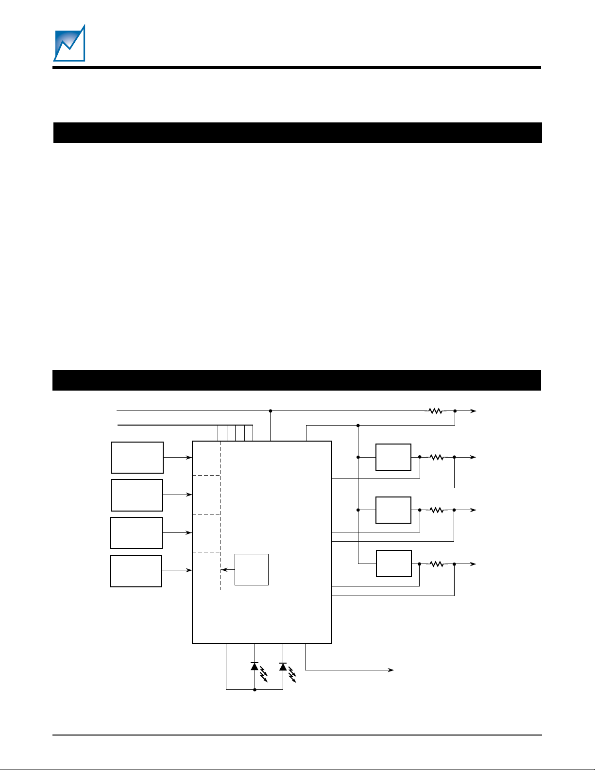
SIMPLIFIED APPLICATION DRAWING
5V
2
I
C
EXT. TEMP .
SENSOR
CURRENT
SENSOR
CH0
CH1
SMD1108
AIRFLOW
SENSOR
ENVIRON-
MENTAL
MONITOR
CH2
CH3
Internal
Temp.
Sensor
AUXVCC
SMBALERT
/CH4
CC0
V
RDY#
V
V
V
CC1
CC2
CC3
OC0
/CH5
OC1
/CH6
OC2
/CH7
OC3
RST#
OC0OC0OC0OC0
LDO
LDO
LDO
5V
3.3V
2.5V
1.8V
RESET#
2052 SAD
©SUMMIT MICROELECTRONICS, Inc., 2001 • 300 Orchard City Dr., Suite 131 • Campbell, CA 95008 • Phone 408-378-6461 • FAX 408-378-6586 • www.summitmicro.com
Characteristics subject to change without notice
2052 2.0 10/05/01
1

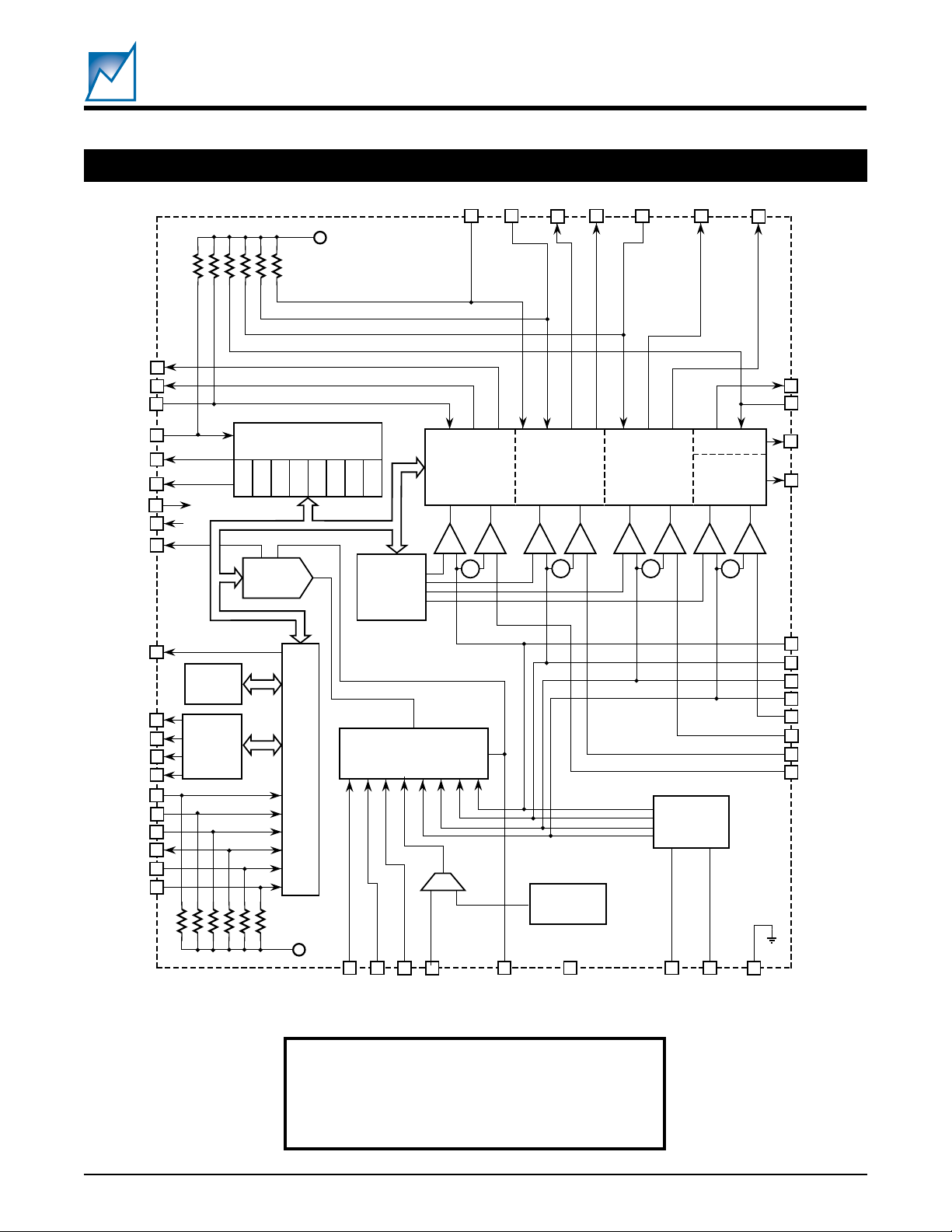
FUNCTIONAL BLOCK DIAGRAM
SMD1108
Preliminary
DLYD_RST#
RST#
MR#
AUTOMON
LIM_IRQ#
SMB
ALERT
V
REFIN
V
REFOUT
RDY#
AUXV
GPO-0
GPO-1
GPO-2
GPO-3
A0
A1
A2
SDA
SCL
CE#
OV_IRQ#
12
13
V
CC
All Resistors
are 100k
Ω
WD_EN# LDO#
WLDI
WDO#
48
3
1
2
IRQ_RST#
7
OC_IRQ#
14
15
5
9
11
4
Programmable Combi-
natorial Logic
Hi
Hi
Lo
0
0
Hi
Lo
1
2
1
Lo
Nonvolatile
Programmable
Hi
Lo
3
3
2
Combinatorial
Reset Logic
Reset Timer
Nonvolatile
Programmable
Watchdog
Timer
Logic
Programmable
Combinatorial
Interrupt
Logic
Nonvolatile
Status
Register
23
HEALTHY#
UV_OVRD
16
24
FAULT#
10
FAULT_IRQ#
29
20
6
10-Bit
ADC
42
CC
Memory
Array
28
27
26
25
43
44
Four
General
Purpose
Outputs
Serial Interface
Reference
Select
& Trim
Logic
Programmable
NV-OU
Octal Analog
Switch
–
+
50
mV
45
NV-OU
–
+
–
+
50
mV
NV-OU
–
+
–
+
+
50
mV
Control &
Distribution
NV-OU
–
Power
–
–
+
+
50
mV
41
V
/CH4
CC0
40
V
/CH5
CC1
39
V
/CH6
CC2
38
/CH7
V
CC3
34
OC3
35
OC2
36
OC1
37
OC0
46
47
22
All Resistors
are 100k
Ω
Temperature
Sensor
V
CC
33
CH0
32
CH1
31
CH2
30
CH3
19
AGND
21
Reserved
17
PGND
18
DGND
8
GND
2052 BD 1.1
RECOMMENDED OPERATING CONDITIONS
Temperature –40ºC to 85ºC.
Voltage 2.7V to 5.5V
2
2052 2.0 10/05/01
SUMMIT MICROELECTRONICS, Inc.

INTRODUCTION
SMD1108
Preliminary
The SMD1108 is a versatile, programmable 8-channel,
10-bit Data Acquisition System that is designed to operate
autonomously, relieving the system host and logic board
of the environmental monitoring tasks.
PIN CONFIGURATION
48-Pin TQFP
WLDI
SCL
SDAA2A1A0AUXV
Programming of configuration, control and calibration
values by the user can be simplified with the interface
adapter and Windows GUI software obtainable from
Summit Microelectronics.
CC
/CH4
/CH5
/CH6
/CH7
CC0
CC1
CC2
V
CC3
V
V
V
OC0
LDO#
WDO#
WD_EN#
SMB
ALERT
MR#
RDY#
IRQ_RST#
GND
AUTOMON
FAULT_IRQ#
LIM_IRQ#
OC_IRQ#
4847464544434241403938
1
2
3
4
5
6
7
8
9
10
11
12
1314151617181920212223
RST#
PGND
DGND
AGND
OV_IRQ#
UV_OVRD
V
DLYD_RST#
CE#
REFOUT
Reserved
37
OC1
36
OC2
35
34
OC3
CH0
33
CH1
32
CH2
31
CH3
30
V
29
GPO-0
28
GPO-1
27
GPO-2
26
GPO-3
25
24
FAUALT#
2052 PCon 1.0
HEALTHY#
REFIN
SUMMIT MICROELECTRONICS, Inc.
2052 2.0 10/05/01
3

ABSOLUTE MAXIMUM RATINGS
SMD1108
Preliminary
Temperature Under Bias ...................... –55°C to 125°C
Storage Temperature ........................... –65°C to 150°C
Lead Solder Temperature (10s) ......................... 300 °C
Output Short Circuit Current ........................ # 100mA
Terminal Voltage with Respect to GND (AGND,
DGND & PGND tied):
Digital Inputs:IRQ_RST#, WD_EN#, MR#, WLDI, SCL,
Digital Outputs: ................. LDO#, WDO#, SMB
HEALTHY#, FAULT_IRQ#, LIM_IRQ#,
OC_IRQ#, RST#, OV_IRQ#, DLYD_RST#,
FAULT#, RDY#, GPO-0, GPO-1, GPO-2, and
GPO-3 ............................................. –2V to 7V
Analog Inputs: V
V
CC3
CC0
/CH7, CH0, CH1, CH2, CH3, OC1, OC2,
OC3, AUXVCC, and V
CE#, A0, A1, A2, and AUTOMON .... –2V to 7V
#
Output shorted for no more than one second, no more
than one output shorted at a time.
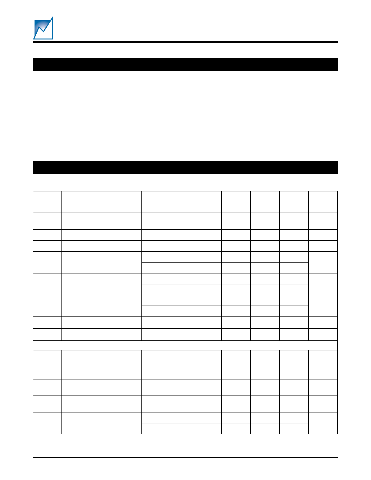
DC OPERATING CHARACTERISTICS
(Over Recommended Operating Conditions; Voltages are relative to GND)
lobmySretemaraPsnoitidnoC )1etoN( .niM.pyT.xaMstinU
I
CC
I
BS
I
IL
I
OL
V
1LO
V
2LO
V
HO
V
LI
V
HI
tuOtnerrucegakaeltupV
stupnIgolanA
V
V
V
V
I
Note 1: Unless otherwise specified VCC is the highest of the four V
V
NIFER
1NI
2NI
3NI
ORV
FER
hguorhtVCC3HC/3
V
TUOFER
tnerruCylppuSnepostuptuollA13Am
tnerruCybdnatS
tnerrucegakaeltupnIV
egatlovwoltuptuO
egatlovwoltuptuO
egatlovhgihtuptuO
NI
TUO
I
LO
I
LO
V
CC
V
CC
V
CC
V
CC
VotV0=
CC
VotV0=
CC
Am5=4.0
Am1=4.0
I,V5=
LO
I,V5.4<
LO
I,V5=
LO
I,V5.4<
LO
,eldiCDA,nepostuptuollA
ssecorpniyromemon
Am1.2=4.0
Am1=2.0
Am004–= 4.2
Am001–=V
CC
egatlovwoltupnI1.0– 3.0 × V
egatlovhgihtupnI2V
egatlovtupni15V
VnoegatlovtupnI
7hguorht
3COhguorht
tnerruc
0HC/0
CC
4slennahcnoegatlovtupnI
0COnoegatlovtupnI
V
TUOFER
V
TUOFER
V5.2=1
V840.2=1
/CHX inputs.
CCX
05.5V
02× V
0V
/CH4, V
2.0–
ALERT
/CH5, V
CC1
IN .............. –2V to 7V
REF
CC2
/CH6,
1.01Am
2Aµ
01Aµ
CC
1+V
CC
NIFER
CC
2052 Elect Table 1.0
#,
V
V
V
V
V
V
Am
4
2052 2.0 10/05/01
SUMMIT MICROELECTRONICS, Inc.

PIN DESCRIPTIONS
V
/CH4 – V
CC0
These 4 inputs are used as the voltage monitor inputs and
the voltage supply for the SMD1108. Internally they are
diode ORed and the input with the highest voltage potential will be the default supply voltage. For proper device
operation at least one of the inputs must be at 2.7V or
higher. V
CC0
programmable comparators. The under-voltage and
over-voltage threshold voltage of each comparator is
programmable.
V
(29)
REFIN
A reference voltage for the ADC. The user can select
either the VREFIN as the ADC reference or use the default
internal reference voltage.
V
REFOUT
(20)
The internally generated reference voltage. It is programmable and can supply either 2.048V or 2.500V.
AGND, DGND, PGND, GND (19, 18, 17, 8)
These are the analog, digital, package, and common
ground inputs, respectively. They should all be tied to the
same ground plane.
/CH7 (38, 39, 40, 41)
CC3
/CH4 to V
/CH7 are also inputs to four
CC3
SMD1108
Preliminary
SDA (46)
Serial data input/output pin. It should be tied to V
through a 10kΩ pull-up resistor.
SCL (47)
Serial clock input pin. It should be tied to VCC through a
10kΩ pull-up resistor.
CH0 to CH3 (33, 32, 31, 30)
The analog channel inputs. These inputs are monitored
solely through the use of the ADC.
OC0 to OC3 (37, 36, 35, 34)
Over-current sense inputs. They are paired with VCC0/
CH4 to VCC3/CH7, respectively, and have a fixed 50mV
offset with respect to their corresponding channel input.
MR# (5)
An active low manual reset input. When MR# is driven low
the reset output will immediately be driven low. MR# is not
maskable and will always generate a reset sequence. The
duration of the RST# pulse will be equal to the length of the
MR# input pulse plus the programmed reset time-out
period value.
CC
AUXVCC (42)
AUXVCC should be isolated from the system power
supplies and tied to ground through capacitor C
normal device operation C
will be charged by the
B/U
. During
B/U
system supplies through the SMD1108. If system power
is lost the charge on C
will be used to store the status
B/U
of the monitor inputs. A 10µF tantalum capacitor should
be used for C
B/U
.
In the system environment AUXVcc could also be connected to the front of the card (along with SDA and SCL
and GND) so that power could be applied to the SMD1108
to read the contents of the NV status registers.
A0, A1 and A2 (43, 44, 45)
Address inputs. When addressing the SMD1108 either as
a memory or an analog channel (or configuration register)
the address inputs distinguish which one of eight possible
devices sharing the common bus is being addressed.
CE# (22)
A control mechanism for the 2-wire interface. The true
state polarity is programmable. When driven true the
interface is active and communications channels are
open. When it is driven false all communications via the
bus are disabled.
WD_EN# (3)
The enable input for both the Watchdog and the Longdog.
It must be driven low to enable the operation of their
timers. This can provide a convenient mechanism during
“debug of code” or during a “power-on configuration”
sequence.
WLDI (48)
The Watchdog timer interrupt input. A low to high
transition on WDI will reset the Watchdog and Longdog
timers. If the timer is not reset within the programmed
period of time the SMD1108 will activate the WDO# output
first and then the LDO# output.
RST# (15)
An active low open drain output. It will be driven low by
the combination of VCC0/CH4 to VCC3/CH7 being at
levels below their programmed settings and/or MR# being
driven low. RST# will stay low for the duration of the fault
condition or the MR# low input and remain low for the
duration of t
after the removal of the fault condition
PURST
or MR# returning high.
SUMMIT MICROELECTRONICS, Inc.
2052 2.0 10/05/01
5

SMD1108
Preliminary
DLYD_RESET# (14)
An active low open drain output. During normal system
operation it will be driven low by the combination of VCC0/
CH4 to VCC3/CH7 being at levels below their programmed settings. During the power-on sequence it will
be delayed to allow the system to power-up in a controlled
sequenced order. See Table 19 for the delay values.
SMB
ALERT
# (4)
An active low open drain output. It will be driven low
whenever one or more of the four auto-monitor inputs
exceeds its limits. Once the SMB
# output is driven
ALERT
low the SMD1108 will respond to the industry standard
SMB protocol and identify itself as the generator of the
alert.
LIM_IRQ# (11)
An active low open drain output that is programmable to be
driven low whenever any one of the selected auto-monitor
inputs exceeds the programmed high or low value.
FAULT# (24)
An open drain output that can be programmed to drive the
output low whenever a selected source is out of limits
(FAULT#). Conversely it can be programmed to drive the
output low (FAULT) whenever the selected sources are
within limits.
HEALTHY# (23)
An open drain output that can be programmed to drive the
output low whenever a selected source is out of limits
(HEALTHY). Conversely it can be programmed to drive
the output low whenever the selected sources are within
limits (HEALTHY#).
WDO# (2)
Watchdog Timer Output is an active low open drain output
that can be wire-ORed with any number of open drain
outputs. Whenever the programmed time-out period of
the Watchdog timer is exceeded this output will be driven
low.
RDY# (6)
An active low status output indicating the ADC has no
conversion ongoing and the SMD1108 can be accessed
via the serial interface without risk of disturbing a conversion.
GPO-0 to GPO-3 (28, 27, 26, 25)
General purpose outputs that can be accessed via the
two-wire serial interface. The register controlling these
outputs is located in the GFS register section. The GPx
outputs are open drain and will be active when a “1” is
written to the corresponding bit position in GFS Register
0x98. The SMD1108 will power-up with the GPx bits
cleared; therefore, the outputs will not be actively driven.
AUTOMON (9)
This input must be high to enable the Auto Monitor
function.
OV_IRQ# (13)
This is an active low open drain output that is driven low
when the selected over-voltage conditions are true.
OC_IRQ# (12)
This is an active low open drain output that is driven low
when the selected over-current conditions are true.
IRQ_RST# (7)
The IRQ# outputs are latched. Strobing this signal low will
reset the IRQ# outputs. They can also be cleared by
accessing Register 99 (see Table 29).
UV_OVRD (16)
Forcing this input high will disable Under-Voltage reset
conditions.
FAULT_IRQ# (10)
This is an active low open drain output that is driven low
when the selected fault conditions are true.
LDO# (1)
Longdog Timer Output is an active low open drain output
that can be wire-ORed with any number of open drain
outputs. Whenever the programmed time-out period of
the Longdog timer is exceeded this output will be driven
low.
6
2052 2.0 10/05/01
SUMMIT MICROELECTRONICS, Inc.

DEVICE OPERATION
SMD1108
Preliminary
THE ADC AND THE ANALOG SWITCH
10-bit ADC
The 10-bit ADC is a self-clocking SAR implementation. In
the manual mode of conversion the sample and hold
operation will begin after the SMD1108 has received the
request for conversion and the channel address. See
Table 1.
8 Analog Channels
The eight analog channels can be separated into two
function blocks: the bottom four channels (V
V
/CH7) are primarily supply voltage monitors; the top
CC3
CC0
/CH4 to
four channels (CH0 to CH3) are primarily environmental
monitors. All eight channels can be switched to the 10-bit
ADC and have their inputs converted on-command. CH0
to CH3 may be placed in the Auto-Monitor mode.
V
/CH4 to V
CC0
/CH7 provide four inputs to the analog
CC3
switch that controls the analog inputs to the ADC converter. Although these channels cannot be placed in the
Auto-Monitor mode, the host can request a direct conversion.
Because these channels are designed to operate as
supply voltage monitors they are each tied into a programmable comparator. The comparator threshold voltage is
programmable and the polarity of the threshold is programmable. This allows very precise monitoring of underor over-voltage conditions. Paired with each of these
.Cº52@oitaresioNotlangiS.nomBd07
DHT.nimBd08–
cinomrahkaeP
redrodn2.nimBd08–
noitaludomretni
noitrotsid
redrodr3.nimBd08–
52@emitnoisrevnoC º .C.monsµ08
ycaruccACD
noituloseRstib01
gnissimonhcihwrofnoitulosermuminiM
deetnaraugerasedoc
stib01
ycaruccaevitaleRBSL½±
LNDBSL1±
rorreelacsllufevitisoPBSL2±
V
rorretesfforalopnU
V
V5=
CC
CC
CC
V6.3otV7.2=
V7.2otV8.1=
BSL2±V
2052 Table01
Table 1. Typical ADC Performance
channels is an over-current input (OC0 to OC3) that is
offset from its partner comparator by 50mV.
TIMER FUNCTIONS
WATCHDOG and LONGDOG
The SMD1108 has two programmable Watchdog timers
each with its own output (WDO# and LDO#) and a common reset input (WLDI). Both are independently programmable and both can be placed in an idle mode. See
Register 8C.
RST#
This reset output is intended to be used to drive the
backend logic. It is an active low open drain output that is
driven low whenever V
CC0
, V
CC1
, V
CC2
or V
is below its
CC3
programmed threshold and/or MR# is being driven low. It
will stay low for the duration of the fault condition or the
MR# low input and remain low for the duration of t
PURST
(the programmed reset pulse width) after removal of the
fault condition or MR# returning high. It will also be driven
low whenever an over-current condition is detected. See
Register 8C.
DLYD_RST#
This output is activated by the same set of conditions as
RST#. However, during a power-up operation it will not be
immediately asserted. As soon as power to one of the
V
/CH4 to V
CC0
/CH7 inputs is detected a time-out
CC3
sequence will be started. The time-out period is programmable and should be equal to or greater than the worst
case power-on skew between all the supplies being monitored. If all of the supplies have not reached their threshold
before the time-out period, DLYD_RST# will be asserted.
DLYD_RST# can then be used to disable a voltage
sequencer such as the SMH4803A or SMH4804. See
Register 8D.
OUTPUTS
FAULT and HEALTHY
Two programmable outputs (active high or active low) that
will respond to programmed source activators. See Registers 8F and 90 through 95.
IRQs
The interrupt outputs are active low open drain outputs
that are driven low whenever one of the corresponding
monitor inputs senses an excursion beyond its programmed value. See Registers 88, 89, and 98 through 9F.
SUMMIT MICROELECTRONICS, Inc.
2052 2.0 10/05/01
7

SMD1108
Preliminary
SERIAL INTERFACE
The SMD1108 has an industry standard 2-wire serial
interface. It supports four (4) device-type addresses:
1010 for reading and writing the memory array; 1001 for
reading and writing the nonvolatile limit registers and
t
t
SCL
t
SDA In
SDA Out
R
SU:SDA
t
F
t
HD:SDA
t
AA
HIGH
t
HD:DAT
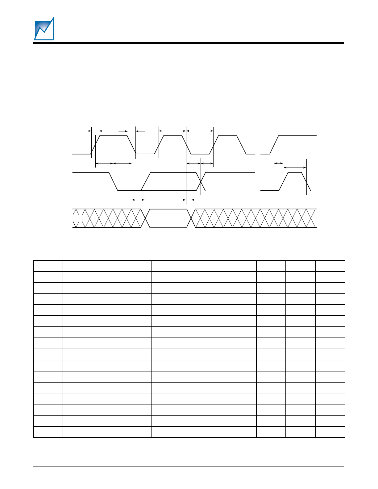
Figure 1. Memory Timing
initiating ADC conversions; 1011 for access to the configuration registers, and 0001 that is used for responses to the
SMB
ALERT
protocol
In order to facilitate host system presence detection
techniques the SMD1108 provides A0, A1 and A2 address
inputs.
t
LOW
t
SU:DAT
t
DH
t
SU:STO
t
BUF
2052 Fig01 1.0
lobmySretemaraPsnoitidnoC.niM.xaMstinU
f
LCS
t
WOL
t
HGIH
t
FUB
t
ATS:US
t
ATS:DH
t
OTS:US
t
AA
t
HD
t
R
t
F
t
TAD:US
t
TAD:DH
ycneuqerfkcolcLCS 0001zHk
doirepwolkcolC 7.4sµ
doirephgihkcolC 0.4sµ
)1(emiteerfsuBnoissimsnartwenerofeB7.4sµ
emitputesnoitidnoctratS 7.4sµ
emitdlohnoitidnoctratS 0.4sµ
emitputesnoitidnocpotS 7.4sµ
tuptuodilavotegdekcolC)nelcyc(ADSdilavotwolLCS3.05.3sµ
)1(emitdlohtuOataDegnahcADSot)1+nelcyc(wolLCS3.0sµ
)1(emitesirADSdnaLCS 0001sn
)1(emitllafADSdnaLCS 003sn
)1(emitputesnIataD 052sn
)1(emitdlohnIataD 0sn
IT)1(ADSdnaLCSretlifesioNnoisserppusesioN001sn
t
RW
Note (1) These values are guaranteed by design.
emitelcycetirW 5sm
2052 Table02 1.0
Table 2. Memory Timing
8
2052 2.0 10/05/01
SUMMIT MICROELECTRONICS, Inc.

MEMORY AND REGISTER OPERATION
SMD1108
Preliminary
The SMD1108 incorporates a memory that is configured
as a 128 x 8 array. Concatenated with the memory array
are the sixteen registers that hold the upper and lower
limits for ADC comparison tables. Additional registers
provide space for configuration usage. Another space is
provided for individual channel conversion initiations and
reading the conversion data.
All Read and Write operations to memory are handled via
an industry standard two-wire interface. The bus was
designed for two-way, two-line serial communication
between different integrated circuits. The two lines are a
serial data line (SDA), and a serial clock line (SCL). The
SDA line must be connected to a positive supply by a pullup resistor, located somewhere on the bus
Input Data Protocol
The protocol defines any device that sends data onto the
bus as a transmitter and any device that receives data as
a receiver. The device controlling data transmission is
called the Master and the controlled device is called the
Slave. In all cases the SMD1108 will be a Slave device
since it never initiates any data transfers.
One data bit is transferred during each clock pulse. The
data on the SDA line must remain stable during clock high
time, because changes on the data line while SCL is high
will be interpreted as a Start or a Stop condition.
START and STOP Conditions
When both the data and clock lines are high the bus is said
to be not busy. A high-to-low transition on the data line,
while the clock is high, is defined as the Start condition.
A low-to-high transition on the data line, while the clock
is high, is defined as the Stop condition.
Acknowledge (ACK)
Acknowledge is a software convention used to indicate
successful data transfers. The transmitting device, either
the Master or the Slave, will release the bus after
transmitting eight bits. During the ninth clock cycle the
receiver will pull the SDA line low to Acknowledge that it
received the eight bits of data.
The SMD1108 will respond with an Acknowledge after
recognition of a Start condition and its Slave address byte.
If both the device and a Write operation are selected, the
SMD1108 will respond with an Acknowledge after the
receipt of each subsequent 8-Bit word. In the Read mode
the SMD1108 transmits eight bits of data, then releases
the SDA line, and monitors the line for an Acknowledge
signal. If an Acknowledge is detected, and no STOP
condition is generated by the master, the SMD1108 will
continue to transmit data. If the Master leaves the SDA
line high (NACK) the SMD1108 will terminate further data
transmissions and await a Stop condition before returning
to the standby power mode.
Device Addressing
Following a start condition the Master must output the
address of the Slave it is accessing. The most significant
four bits of the Slave address are the device type identifier
(DTI). For the SMD1108 the default memory DTI is
1010
. The next three bits in the serial data stream are
BIN
the device’s bus address. The bus address is assigned by
biasing the A0, A1 and A2 pins into any one of eight unique
addresses. The last bit of the data stream defines the
operation to be performed: when set to 1 a Read operation
is selected; when set to 0 a Write operation is selected.
MEMORY WRITE OPERATIONS
The SMD1108 allows two types of Write operations: byte
Write and page Write. A byte Write operation writes a
single byte during the nonvolatile write period (tWR). The
page write operation allows up to 16 bytes in the same
page to be written during tWR.
Byte Write
After the Slave address is sent (to identify the Slave
device, and a Read or Write operation), a second byte is
transmitted which contains the 8-Bit address of any one
of the 128 words in the array. Upon receipt of the word
address the SMD1108 responds with an Acknowledge.
After receiving the next byte of data it again responds with
an Acknowledge. The Master then terminates the transfer
by generating a Stop condition, at which time the
SMD1108 begins an internal write cycle. While the
internal write cycle is in progress the SMD1108 inputs are
disabled, and the device will not respond to any requests
from the master.
Page Write
The SMD1108 is capable of a 16-byte page Write operation. It is initiated in the same manner as the byte Write
operation, but instead of terminating the Write cycle after
the first data word, the Master can transmit up to 15 more
bytes of data. After the receipt of each byte the SMD1108
will respond with an Acknowledge.
SUMMIT MICROELECTRONICS, Inc.
2052 2.0 10/05/01
9
 Loading...