


Studer is a registered trade mark of Studer Professional Audio GmbH, Regensdorf
Prepared and edited by Copyright by Studer Professional Audio GmbH
Studer Professional Audio GmbH Printed in Switzerland
Technical Documentation Order no. 10.27.5180-1 (0608)
Althardstrasse 30
CH-8105 Regensdorf – Switzerland
http://www.studer.ch
Subject to change
I
A Safety Information
A1 First Aid
In Case of Electric Shock: Separate the person as quickly as possible from the electric power source:
• By switching the equipment off,
• By unplugging or disconnecting the mains cable, or
• By pushing the person away from the power source, using dry insulating
material (such as wood or plastic).
• After having suffered an electric shock, always consult a doctor.
Warning! Do not touch the person or his clothing before the power is turned off,
otherwise you stand the risk of suffering an electric shock as well!
If the Person is Unconscious: • Lay the person down
• Turn him to one side
• Check the pulse
• Reanimate the person if respiration is poor
• Call for a doctor immed iately.
Safety Information
To reduce the risk of electric shock, do not remove covers. No user-serviceable parts inside. Refer servicing to qualified service personnel (i.e.,
persons having appropriate technical training and experience necessary
to be aware of hazards to which they are exposed in performing a repair
action, and of measures to minimize the danger of themselves).
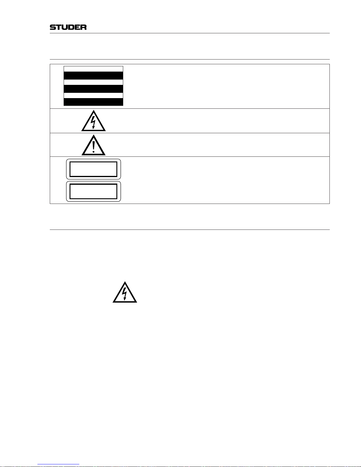
This symbol alerts the user to the presence of un-insulated dangerous volt-
age within the equipment that may be of sufficient magnitude to constitute
a risk of electric shock to a person.
This symbol alerts the user to important instructions for operating and
maintenance in this documentation.
Assemblies or sub-assemblies of this product can contain opto-electronic devices. As long as these devices comply with Class I of laser or
LED products according to EN 60825-1:1994, they will not be expressly
marked on the product. If a special design should be covered by a higher
class of this standard, the device concerned will be marked directly on the
assembly or sub-assembly in accordance with the above standard.
CAUTION
RISK OF ELECTRIC SHOCK
DO NOT OPEN
ACHTUNG
GEFAHR: ELEKTRISCHER SCHLAG
NICHT ÖFFNEN
ATTENTION
RISQUE DE CHOC ELECTRIQUE
NE PAS OUVRIR
CLASS 1
LASER PRODUCT
CLASS 1
LED PRODUCT

II
B General Installation Instructions
Please consider besides these general instructions also any product-specific
instructions in the “Installation” chapter of this manual.
B1 Unpacking
Check the equipment for any transport damage. If the unit is mechanically
damaged, if liquids have been spilled or if objects have fallen into the unit,
it must not be connected to the AC power outlet, or it must be immediately
disconnected by unplugging the power cable. Repair must only be performed
by trained personnel in accordance with the applicable regulations.
B2 Installation Site
Install the unit in a place where the following conditions are met:
• The temperature and the relative humidity of the environment must be
within the specified limits during operation of the unit. Relevant values
are the ones at the air inlets of the unit (refer to Appendix 1).
• Condensation must be avoided. If the unit is installed in a location with
large variation of ambient temperature (e.g. in an OB-van), appropriate
precautions must be taken before and after operation (refer to Appendix
1).
• Unobstructed air flow is essential for proper operation. Air vents of the
unit are a functional part of the design and must not be blocked in any
way during operation (e.g. by objects placed upon them, placement of the
unit on a soft surface, or installation of the unit within a rack or piece of
furniture).
• The unit must not be heated up by external sources of heat radiation (sunlight, spotlights).
B3 Earthing and Power Supply
Earthing of units with mains supply (class I equipment) is performed via
the protective earth (PE) conductor integrated in the mains cable. Units with
battery operation (< 60 V, class III equipment) must be earthed separately.
Earthing the unit is one of the measures for protection against electrical shock
hazard (dangerous body currents). Hazardous voltage may not only be caused
by a defective power supply insulation, but may also be introduced by the
connected audio or control cables.
If the unit is installed with one or several external connections, its earthing
must be provided during operation as well as while the unit is not operated.
If the earthing connection can be interrupted, for example, by unplugging
the mains plug of an external power supply unit, an additional, permanent
earthing connection must be installed using the provided earth terminal.
Avoid ground loops (hum loops) by keeping the loop surface as small as
possible (by consequently guiding the earth conductors in a narrow , parallel
way), and reduce the noise current flowing through the loop by inserting an
additional impedance (common-mode choke).
Installation
III
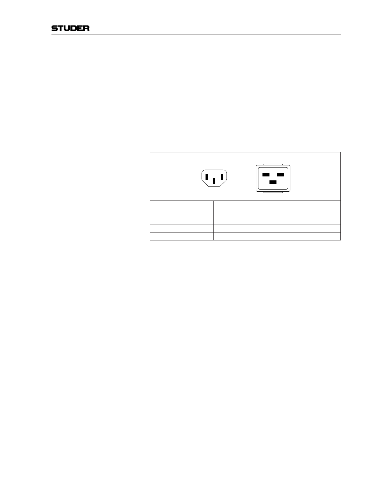
Class I Equipment (Mains Operation)
Should the equipment be delivered without a matching mains cable, the
latter has to be prepared by a trained person using the attached female plug
(IEC 320 / C13 or IEC 320 / C19) with respect to the applicable regulations
in your country.
Before connecting the equipment to the AC power outlet, check that the local
line voltage matches the equipment rating (voltage, frequency) within the
ad missible tolerance. The equipment fuses must be rated in accordance with
the specifications on the equipment.
Equipment supplied with a 3-pole appliance inlet (protection conforming to
class I equip ment) must be connect ed to a 3-pole AC power outlet in such a
way that the equipment ca binet is connected to the protective earth.
For information on mains cable strain relief, please refer to Appendix 2.
Female Plugs (IEC320), Front-Side View:
European Standard
(CENELEC)
North American Standard
(NAS)
Brown
L (Live)
Black
Blue
N (Neutral)
White
Green/Yellow
PE (Protective Earth)
Green (or Green/Yellow)
Class III Equipment (Battery Operation up to 60 VDC)
Equipment of this protection class must be earthed using the provided earth
terminal if one or more external signals are connected to the unit (see explanation at the beginning of this paragraph).
B4 Electromagnetic Compatibility (EMC)
The unit conforms to the protection requirements relevant to electromagnetic
phenomena that are listed in guidelines 89/336/EC and FCC, part 15.
• The electromagnetic interference generated by the unit is limited in such
a way that other equipment and systems can be operated normally.
• The unit is adequately protected against electromagnetic interference so
that it can operate properly.
The unit has been tested and conforms to the EMC standards of the speci-
fied electromagnetic environment, as listed in the following declaration.
The limits of these standards ensure protection of the environment and corresponding noise immunity of the equipment with appropriate probability.
However, a professional installation and integration within the system are
imperative prerequisites for operation without EMC problems.
For this purpose, the following measures must be followed:
• Install the equipment in accordance with the operating instructions. Use
the supplied accessories.
• In the system and in the vicinity where the equipment is installed, use only
components (systems, equipment) that also fulfill the EMC standards for
the given environment.
Installation / EMC
PE
LN
IEC 320 / C19IEC 320 / C13
PE
LN

IV
• Use a system grounding concept that satisfies the safety requirements
(class I equipment must be connected with a protective ground conductor) and that also takes into consideration the EMC require ments. When
deciding between radial, surface, or combined grounding, the advantages
and disadvantages should be carefully evaluated in each case.
• Use shielded cables where shielding is specified. The connection of the
shield to the corresponding connector terminal or housing should have a
large surface and be corrosion-proof. Please note that a cable shield connected only single-ended can act as a transmitting or receiving antenna
within the corresponding frequency range.
• Avoid ground loops or reduce their adverse effects by keeping the loop sur face as small as possible, and reduce the noise current flowing through the
loop by inserting an additional impedance (e.g. common-mode choke).
• Reduce electrostatic discharge (ESD) of persons by installing an appropriate floor covering (e.g. a carpet with permanent electrostatic filaments) and
by keeping the relative humidity above 30%. Further measures (e.g. conducting floor) are usually unnecessary and only effective if used together
with corresponding personal equipment.
• When using equipment with touch-sensitive operator controls, please take
care that the surrounding building structure allows for sufficient capacitive
coupling of the operator. This coupling can be improved by an additional,
conducting surface in the operator’s area, connected to the equipment
housing (e.g. metal foil underneath the floor covering, carpet with conductive backing).
C Maintenance
All air vents and openings for operating elements (faders, rotary knobs) must
be checked on a regular basis, and cleaned in case of dust accumulation. For
cleaning, a soft paint-brush or a vacuum cleaner is recommended.
Cleaning the surfaces of the unit is performed with a soft, dry cloth or a soft
brush.
Persistent contamination can be treated with a cloth that is slightly humidified
with a mild cleaning solution, such as dishwashing detergent.
For cleaning display windows, commercially available computer/TV screen
cleaners are suited. Use only a slightly damp (never wet) cloth.
Never use any solvents for cleaning the exterior of the unit! Liquids must
never be sprayed or poured on directly!
For equipment-specific maintenance information please refer to the corre-
sponding chapter in the operating and service manuals.
EMC / Maintenance

V
D Electrostatic Discharge during Maintenance and Repair
Caution: Observe the precautions for handling devices sensitive to electrostatic dis-
charge!
Many semiconductor components are sensitive to electrostatic discharge
(ESD). The lifespan of assemblies contain ing such components can be drastically reduced by improper handling during maintenance and repair. Please
observe the following rules when handling ESD sensitive components:
• ESD sensitive components should only be stored and transported in the
packing material specifically provided for this purpose.
• When performing a repair by replacing complete assemblies, the r emoved
assembly must be sent back to the supplier in the same packing material
in which the replacement assembly was shipped. If this should not be the
case, any claim for a possible refund will be null and void.
• Unpacked ESD sensitive components should only be handled in ESD protected areas (EPA, e.g. area for field service, repair or service bench) and
only be touched when wearing a wristlet connected to the ground potential
of the service bench by a series resistor. The equipment to be repaired or
serviced as well as all tools and electrically semi-conducting work, storage,
and floor mats should also be connected to this ground potential.
• The terminals of ESD sensitive components must not come in uncontrolled
contact with electro statically chargeable or metallic surfaces (voltage
puncture, discharge shock hazard).
• To prevent the components from undefined transient stress and possible
damage due to inadmissible voltages or compensation currents, electrical
connections should only be established or separated when the equipment
is switched off and after any capacitor charges have decayed.
E Repair
By removing housing parts or shields, energized parts may be exposed. For
this reason the following precautions must be observed:
• Maintenance may only be performed by trained personnel in accordance
with the applicable regulations.
• The equipment must be switched off and disconnected from the AC power
outlet before any housing parts are removed.
• Even if the equipment is disconnected from the power outlet, parts with
hazardous charges (e.g. capacitors, picture tubes) must not be touched until
they have been properly discharged. Do not touch hot components (power
semi con ductors, heat sinks, etc.) before they have cooled off.
• If a unit remains opened while being switched on, no un-insulated circuit com pon ents and metallic semiconductor housings must be touched,
neither with bare hands nor with un- insulated tools.
Certain components pose additional hazards:
• Explosion hazard from lithium batteries, electrolytic capacitors and power
semiconductors (Observe the component’s polarity. Do not short battery
terminals. Replace batteries only by the same type).
• Implosion hazard from evacuated display units.
• Radiation hazard from laser units (non-ionizing), CRTs (ionizing).
• Caustic effect of display units (LCD) and components containing liquid
electrolyte.
Such components should only be handled by trained personnel who ar e prop-
erly protected (e.g. protection glasses, gloves).
ESD / Repair
VI
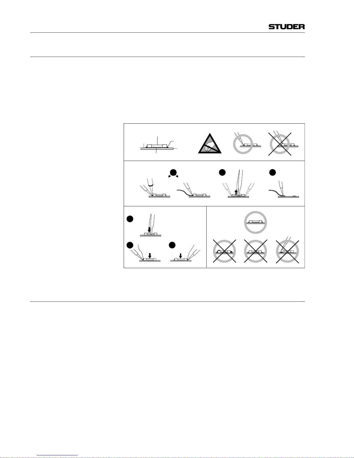
E1 SMD Components
Studer has no commercially available SMD components in stock for ser-
vice purposes. For repair, the corresponding devices have to be purchased
locally . The specifications of special components can be found in the service
manual.
SMD components should only be replaced by skilled specialists using appro-
priate tools. No warranty claims will be accepted for circuit boards that have
been damaged. Proper and improper SMD soldering joints are illustrated
below.
F Disposal
Packing Materials The packing materials have been selected with environmental and disposal
issues in mind. All packing material can be recycled. Recycling packing saves
raw materials and reduces the volume of waste.
If you need to dispose of the transport packing materials, please try to use
recyclable means.
Used Equipment Used equipment contains valuable raw materials as well as materials that
must be disposed of professionally . Please return your used equipment via an
authorized specialist dealer or via the public waste disposal system, ensuring
any material that can be recycled is.
Please take care that your used equipment cannot be abused. To avoid abuse,
delete sensitive data from any data storage media. After having disconnected
your used equipment from the mains supply, make sure that the mains connector and the mains cable are made useless.
Repair / Disposal
Dismounting
Mounting Examples
Solder
SMD
Component
Copper
Track
Adhesive
Soldering Iron
Desoldering
Iron
Desolder
Wick
Heat and Remove Cleaning
Solder
Ø 0.5...0.8 mm
Heating Time < 3 s per Side
Soldering
Iron
Desolder
Wick
PCB
3
2
1
3
2
1

VII
G Declarations of Conformity
G1 Class A Equipment - FCC Notice
This equipment has been tested and found to comply with the limits for a
Class A digital device, pursuant to Part 15 of the FCC Rules. These limits
are designed to provide a reasonable protection against harmful interference when the equipment is operated in a commercial environment. This
equipment generates, uses, and can radiate radio frequency energy and, if
not installed and used in accordance with the instruction manual, may cause
harmful interference to radio com munications. Operation of this equipment
in a residential area is likely to cause harmful interference, in which case the
user will be required to correct the interference at his own expense.
Caution: Any changes or modifications not expressly approved by the manufacturer
could void the user’ s authority to operate the equipment. Also r efer to relevant
information in this manual.
G2 CE Declaration of Conformity
We,
Studer Professional Audio GmbH,
CH-8105 Regensdorf,
declare under our sole responsibility that the product
Studer OnAir 2500, Digital Broadcast Mixing Console
(starting with serial no. 1001),
to which this declaration relates, according to following regulations of EU
directives and amendments
• Low Voltage (LVD):
73/23/EEC + 93/68/EEC
• Electro magnetic Compatibility (EMC):
89/336/EEC + 92/31/EEC + 93/68/EEC
is in conformity with the following standards or normative documents:
• Safety:
EN 60950:2001 (Class I equipment)
• Safety of laser products:
EN 60825-1:1994 + A11 + A2, EN 60825-2:2000
• EMC:
EN 55103-1/-2:1996, electromagnetic environments E2 and E4.
Regensdorf, May 21, 2008
B. Hochstrasser, President M. Lienert, Manager R&D
Conformity

VIII
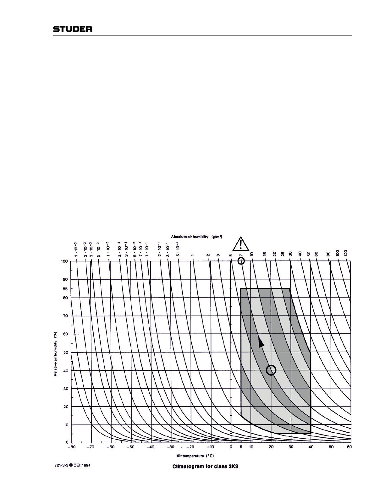
Appendix 1: Air Temperature and Humidity
General
Normal operation of the unit or system is warranted under the ambient condi-
tions defined by EN 60721-3-3, set IE32, value 3K3.
This standard consists of an extensive catalogue of parameters, the most
important of which are: Ambient temperature*, relative humidity 5...85%
(i.e., no formation of condensation or ice); absolute humidity 1...25 g/m³;
rate of temperature change < 0.5 °C/min. These parameters are dealt with in
the following paragraphs.
* Please Note: The ambient temperature range is restricted to +5...+35 °C, as opposed to the
standard mentioned above.
Under these conditions the unit or system starts and works without any prob-
lem. Beyond these specifications, possible problems are described below.
Ambient Temperature
Units and systems by Studer are generally designed for an ambient tempera-
ture range (i.e. temperature of the incoming air) of +5 °C to +40 °C. When
rack mounting the units, the intended air flow and herewith adequate cooling
must be provided. The following facts must be considered:
• The admissible ambient temperature range for operation of the semiconductor components is 0 °C to +70 °C (commercial temperature range for
operation).
• The air flow through the installation must provide that the outgoing air is
always cooler than 70 °C.
• Average heat increase of the cooling air shall be about 20 K, allowing for
an additional maximum 10 K increase at the hot components.
• In order to dissipate 1 kW with this admissible average heat increase, an
air flow of 2.65 m³/min is required.
Example: A rack dissipating P = 800 W requires an air flow of 0.8 * 2.65 m³/min which
corresponds to 2.12 m³/min.
• If the cooling function of the installation must be monitored (e.g. for fan
failure or illumination with spot lamps), the outgoing air temperature must
be measured directly above the modules at several places within the rack.
The trigger temperature of the sensors should be 65 °C to 70 °C.
Frost and Dew
The unsealed system parts (connector areas and semiconductor pins) allow
for a minute formation of ice or frost. However, formation of dew visible to
the naked eye will already lead to malfunctions. In practice, reliable operation can be expected in a temperature range above –15 °C, if the following
general rule is considered for putting the cold system into operation:
If the air within the system is cooled down, the relative humidity rises. If it
reaches 100%, condensation will arise, usually in the boundary layer between
the air and a cooler surface, together with formation of ice or dew at sensitive areas of the system (contacts, IC pins, etc.). Once internal condensation
occurs, trouble-free operation cannot be guaranteed, independent of temperature.
Before putting into operation, the system must be checked for internal for-
mation of condensation or ice. Only with a minute formation of ice, direct
Appendix
IX
evaporation (sublimation) may be expected; otherwise the system must be
heated and dried while switched off.
A system without visible internal formation of ice or condensation should be
heated up with its own heat dissipation, as homogeneously (and subsequently
as slow) as possible; the ambient temperature should then always be lower
than the one of the outgoing air.
If it is absolutely necessary to operate the cold system immediately within
warm ambient air, this air must be dehydrated. In such a case, the absolute
humidity must be so low that the relative humidity, related to the coldest
system surface, always remains below 100%.
Ensure that the enclosed air is as dry as possible when powering off (i.e. before
switching off in winter, aerate the room with cold, dry air , and remove humid
objects such as clothes from the room).
These relationships are visible from the following climatogram. For a con-
trolled procedure, thermometer and hygrometer as well as a thermometer
within the system will be required.
Example 1: An OB-van having an internal temperature of 20 °C and a relative humidity of
40% is switched off in the evening. If the temperature falls below +5 °C, the
relative humidity will rise to 100% (7 g/m³); dew or ice will be forming.
Example 2: An OB-van is heated up in the morning with air of 20 °C and a relative
humidity of 40%. On all parts being cooler than +5 °C, dew or ice will be
forming.
Appendix
X
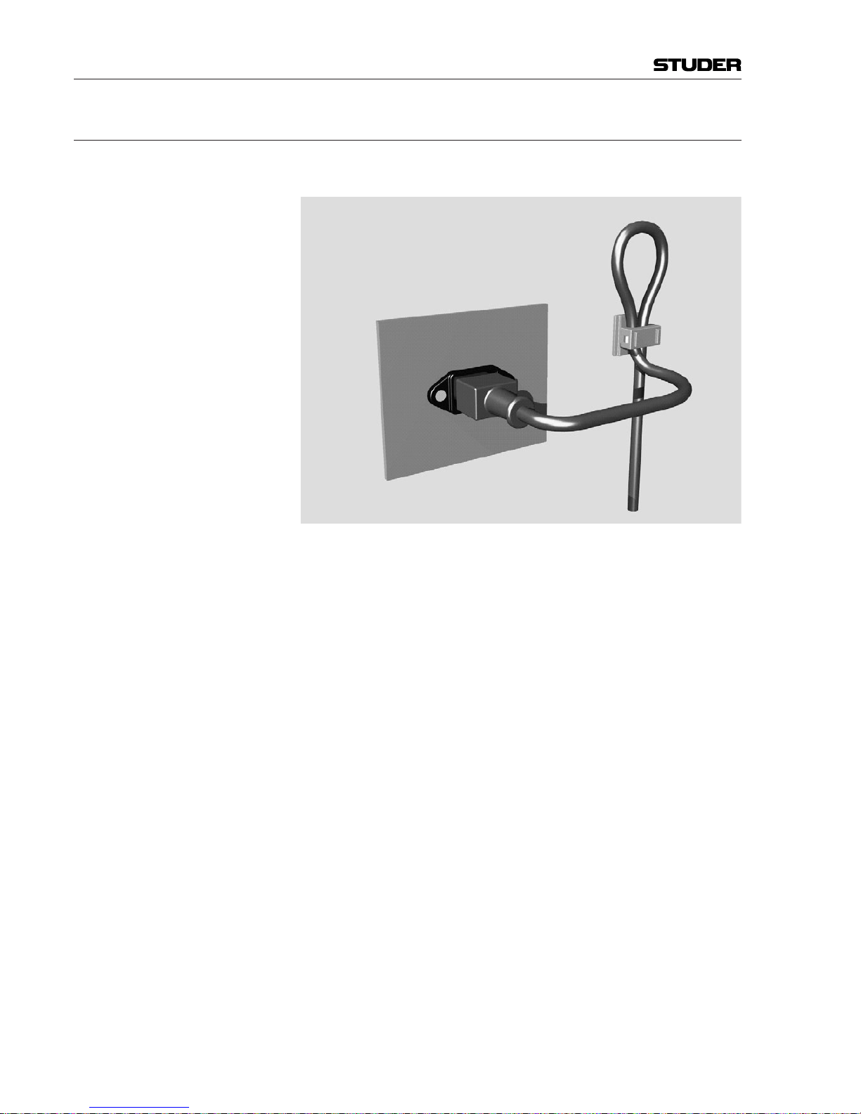
Appendix 2: Mains Connector Strain Relief
For anchoring connectors without a mechanical lock (e.g. IEC mains connec-
tors), we recommend the following arrangement:
Procedure: The cable clamp shipped with your unit is auto-adhesive. For mounting please
follow the rules below:
• The surface to be adhered to must be clean, dry , and free from grease, oil,
or other contaminants. Recommended application temperature range is
+20 °C to +40 °C.
• Remove the plastic protective backing from the rear side of the clamp
and apply it firmly to the surface at the desired position. Allow as much
time as possible for curing. The bond continues to develop for as long as
24 hours.
• For improved stability, the clamp should be fixed with a screw. For this
purpose, a self-tapping screw and an M4 bolt and nut are included.
• Place the cable into the clamp as shown in the illustration above and firmly
press down the internal top cover until the cable is fixed.
Appendix

XI
Appendix 3: Software License
Use of the software is subject to the Studer Professional Audio Software
License Agreement set forth below. Using the software indicates your acceptance of this license agreement. If you do not accept these license terms, you
are not authorized to use this software.
Under the condition and within the scope of the following Terms and Con-
ditions, Studer Professional Audio GmbH (hereinafter “Studer”) grants the
right to use programs developed by Studer as well as those of third parties
which have been installed by Studer on or within its products. References
to the license programs shall be references to the newest release of a license
program installed at the Customer’s site.
Programs Covered by the Agreement
License Programs of Studer The following Terms and Conditions grant the right to use all programs of
Studer that are part of the System and/or its options at the time of its delivery
to the Customer, as well as the installation software on the original data disk
and the accompanying documentation (“License Material”). In this Agreement the word “Programs” shall have the meaning of programs and data
written in machine code.
Using the software indicates your acceptance of this license agreement. If
you do not accept these license terms, you are not authorized to use this software.
Programs of Third Parties Programs of third parties are all programs which constitute part of the System
and/or its options at the time of delivery to the Customer but have not been
developed by Studer. The following conditions are applicable to programs of
third parties:
• The right to use third parties’ programs is governed by the License Agreement attached hereto (if applicable), which is an integral part of this Agreement. The Customer shall sign any and all License Agreements for all
further programs of third parties installed on the system. The Customer
shall be deemed to have received all License Agreements upon delivery
of the system and/or its options.
• Studer shall accept no responsibility or liability for, and gives no warranties (express or implied) as to the programs of third parties. The Customer
waives any and all claims versus Studer for any consequential damages,
which might occur due to defects of these programs.
Right of Use
Principle Studer grants the Customer the non-exclusive right to use the License Ma-
terial in one copy on the system and/or its options as laid down by the Sales
Agreement concluded between the parties and all Terms and Conditions
which shall be deemed to form and be read and construed as part of the
Sales Agreement. This right is assignable according to the “Assignability”
paragraph hereinafter.
Appendix

XII
Customized Configurations The Customer is not entitled to alter or develop further the License Material
except within the expressly permitted configuration possibilities given by the
software installed on the system or elsewhere. All altered programs, including but not limited to the products altered within the permitted configuration
possibilities, are covered by this License Agreement.
Reverse Engineering Reverse engineering is only permitted with the express consent of Studer.
The consent of Studer can be obtained but is not limited to the case in which
the interface software can not be provided by Studer. In any case Studer has
to be informed immediately upon complete or partial reverse engineering.
Copying the License Material The Customer is entitled to make one copy of all or parts of the License
Material as is necessary for the use according to this Agreement, namely for
backup purposes. The Customer shall apply the copyright of Studer found on
the License Material onto all copies made by him. Records shall be kept by
the Customer regarding the amount of copies made and their place of keeping.
The responsibility for the original program and all copies made lies with the
Customer. Studer is entitled to check these records on first request. Copies
not needed anymore have to be destroyed immediately.
Disclosure of License Material The License Material is a business secret of Studer. The Customer shall not
hand out or in any way give access to parts of or the complete License Material
to third parties nor to publish any part of the License Material without prior
written consent of Studer. The Customer shall protect the License Material
and any copies made according to the paragraph above by appropriate defense
measures against unauthorized access. This obligation of non-disclosure is a
perpetual obligation.
Third parties are entitled to have access to the License Material if they use the
License Material at the Customer’s site in compliance with this Agreement.
Under no circumstance are third parties entitled to have access to the instal-
lation software on the original data media. The Customer shall safeguard the
original data media accordingly.
Assignability The rights granted to the Customer according to this License Agreement shall
only be assignable to a third party together with the transfer of the system
and/or its options and after the prior written consent of Studer.
Rights to License Material
With the exception of the right of use granted by this License Agreement all
proprietary rights to the License Material, especially the ownership and the
intellectual property rights (such as but not limited to patents and copyright)
remain with Studer even if alterations, customized changes or amendments
have been made to the License Material.
Studer’s proprietary rights are acknowledged by the Customer. The Customer
shall undertake no infringements and make no claims of any patent, registered
design, copyright, trade mark or trade name, or other intellectual property
right.
Warranty, Disclaimer, and Liability
For all issues not covered herewithin, refer to the “General Terms and Condi-
tions of Sales and Delivery” being part of the sales contract.
Appendix
WIRING – IMPORTANT
The OnAir 2500 ST MON and LAN wiring must comply with the
following requirements:
Cable Type: Cat 5e, with shielded connectors on both ends.
Cable Dimensions:
Max. Length for
Monitoring/TB Module
Min.
AWG
Minimum
Sectional Area
100 m 24 0.21 mm
2
60 m 26 0.13 mm
2
Details: Cat(egory) 5e Cable is an enhanced version of Cat 5 that adds specifi cations for far-end cross-
talk. It replaced the specifi cation for Cat 5 with the 2001 introduction of the
TIA/EIA-568-B standard. Cat 5e cable performance characteristics and test
methods are defi ned in TIA/EIA-568-B.2-2001.
ST MON (RS422) Cables (both ends w. shielded connectors) from the ST MON socket to a monitoring/
TB module:
ST MON socket
Wire Color
Monitoring/TB Module
Signal Pin Pin Signal
+24 V *
1
2
wht/org
org
1
2
+24 V *
RX+ 3 wht/grn 3 TX+
TX+ 4 blu 4 RX+
TX– 5 wht/blu 5 RX–
RX– 6 grn 6 TX–
Gnd *
7
8
wht/brn
brn
7
8
Gnd *
* Caution: Connectors are identical on the ST MON and the LAN cables. Make sure not
to mix them up since the ST MON socket carries DC supply voltage!
LAN (Ethernet) Cables (both ends w. shielded connectors) for connection of the console to e.g. a
router or an existing OnAir 3000 network. Since modern hubs and switches
have auto polarity selection, straight-through cables may be used in any
case.
Signal Pin
Wire Color
Pin Signal
TX+ 1 wht/org 1 TX+
TX– 2 org 2 TX–
RX+ 3 wht/grn 3 RX+
4 blu 4
5 wht/blu 5
RX– 6 grn 6 RX–
7 wht/brn 7
8 brn 8
Top (tab
down):
18
18
Front:
Top (tab
down):
18
18
Front:
Date printed: 09.06.08
SW V3.0
OnAir 2500 Digital Mixing Console
Important

Date printed: 09.06.08
SW V3.0
OnAir 2500 Digital Mixing Console
Important

1

2
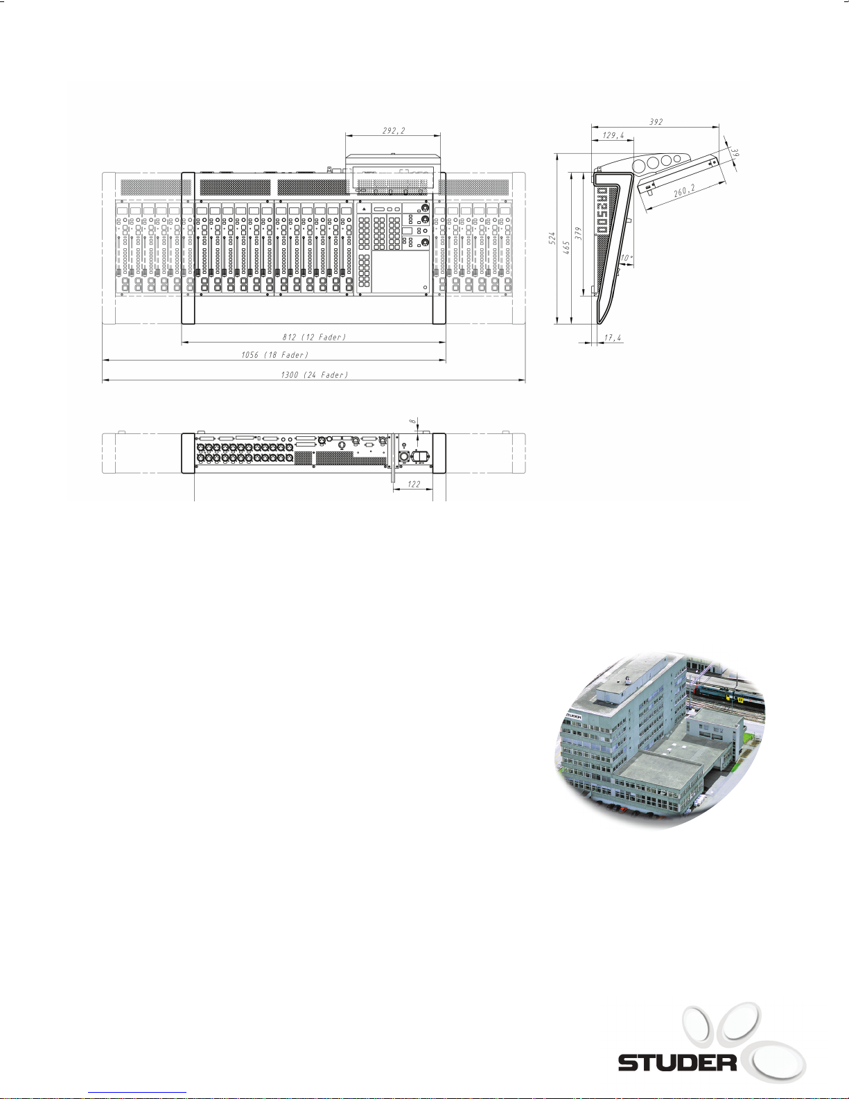
All-in-one Design
The Studer OnAir 2500 ensures a
new standard in ease-of-use for Radio
or TV Broadcast. Designed as
an integrated system – control
surface, I/O breakout, DSP and
controller boards, as well as power
supply, share the same chassis - it
addresses the medium segment of the
live broadcast market including both
private and public network stations.
Its self-contained architecture without
an external core reduces wiring
complexity and setup time to a
minimum. This makes the OnAir 2500
the OnAir 3000. Full compatibility
with other systems of the OnAir
family and a short learning curve
for operators with OnAir 3000
experience are only two of many
advantages.
the ideal audio mixing console for OB
applications, where robustness and
reliability are a must.
Studer’s OnAir 2500 user-interface
builds upon the highly acclaimed
operational concept of the OnAir
2000 and OnAir 3000. Having been
introduced to the market with the
very successful OnAir 2000, Studer’s
patented “Touch’n’Action” philosophy
is incorporated into the OnAir 2500.
The OnAir 2500 even runs the
same mature software platform as
3
OnAir 2500 Key Features:
• 12, 18 or 24 fader layout with
motorised or non-motorised
100mm faders
• Touch sensitive, central 12”
coloured screen with 4 encoders
for parameter adjustment
• OLED (Organic LED) in fader
and central module for clear
readability
• Ergonomic, easy to learn
Touch’n’Action user interface
• Complete integration with Radio
Automation Systems
• Integrated monitoring system
• 8 stereo N-1 busses
• Built-in full channel processesing
with 4-band parametric EQ

4
Ready For Broadcast – Whenever
And Wherever You Want
Like all other products in Studer’s
OnAir portfolio, the OnAir 2500
provides you and your operators with
a wide and well-balanced broadcast
feature set. Typical functions for
your every day work, like muting the
monitor speaker signal while
microphones are open, are already
integrated and need not be
configured, saving time and money.
Nonetheless, nearly all functions can
be easily activated, deactivated or
customised using the configuration
user interface on the main screen.
The ergonomic design and the
simple usability of the OnAir
2500 means that it’s ideally suited to
stressful live on-air operation. Being
under continuous time pressure, the
DJ can change from live presentation
to off air recording, from
pre-conferencing to OB connections.
operation have highest priority. The
OnAir 2500 is entirely geared to
let your talents do their job: making
radio.
The OnAir 2500 supports your daily
work even more. In most
installations, the console will be
operated in a multiuser environment.
Therefore, you can create
user accounts defined with individual
access restrictions on specified
console functions. This applies as
well for the system snapshots, which
are stored internally and contain
custom sets of signal parameters,
crosspoint settings and channel
assignment. According to the
configured rights, users may have
access to only a limited number of
snapshots. Independently, it is possible
to store snapshots externally on a
USB memory stick, connected to a
socket on the main screen.
With the OnAir 2500, Studer has
defined a new standard in ease-of use
for radio broadcast. Like no other
console, the OnAir 2500 with its
compact architecture is the ideal
solution for your mobile applications,
especially because it does not need
any external DSP core. Every signal
you need is connected directly to the
rear panel. No wasted time setting up
links to cores and networks, the
intuitive architecture ensures you’re
on-air fast!
This is where simple and intuitive

5
Studer’s OnAir 2500 is designed as an
integrated system – control surface,
I/O breakout, DSP and controller
boards, as well as power supply,
share the same chassis. Modules of
6 faders build the basis for the three
available consoles sizes with 12, 18 or
24 faders. A central module in every
console layout provides the operators
with a monitoring section, on air
indication, a talkback section and a
built-in talkback microphone.
further reinforces the mobile
capability.
Pushbuttons throughout the entire
console are made of silent rubber
pads, guaranteeing noiseless operation
and perfect tactile feedback.
Despite its compactness, the OnAir
2500 can be easily extended. When
installed in a control room and
connected to a voice booth, a
talkback and monitoring module
(1.943.444 or 1.943.447) can be
attached to enable communication
between engineer and journalist, or
even from the voice booth to any
other destination, e.g. the N-X
returns. Additonally, this extension
includes an independent studio
monitoring module with separate
The talkback and monitoring module
is connected directly to the OnAir
2500 via ADAT (audio) and CAT5
(control). The respective interfaces on
the rear panel are already
preconfigured for this purpose.
To allow fail-safe operation in case of
mains power loss, Studer offers an
external power supply for the OnAir
2500, in a smart 1RU 19” chassis. This
used as secondary feed providing
This all-in-one design is characterised
by a very small footprint. The
smallest version of the OnAir 2500
with 12 faders requires only 80x50
cm and the total weight of 17kgs
volume control for studio speakers
and headphones.
24V DC to the console.

6
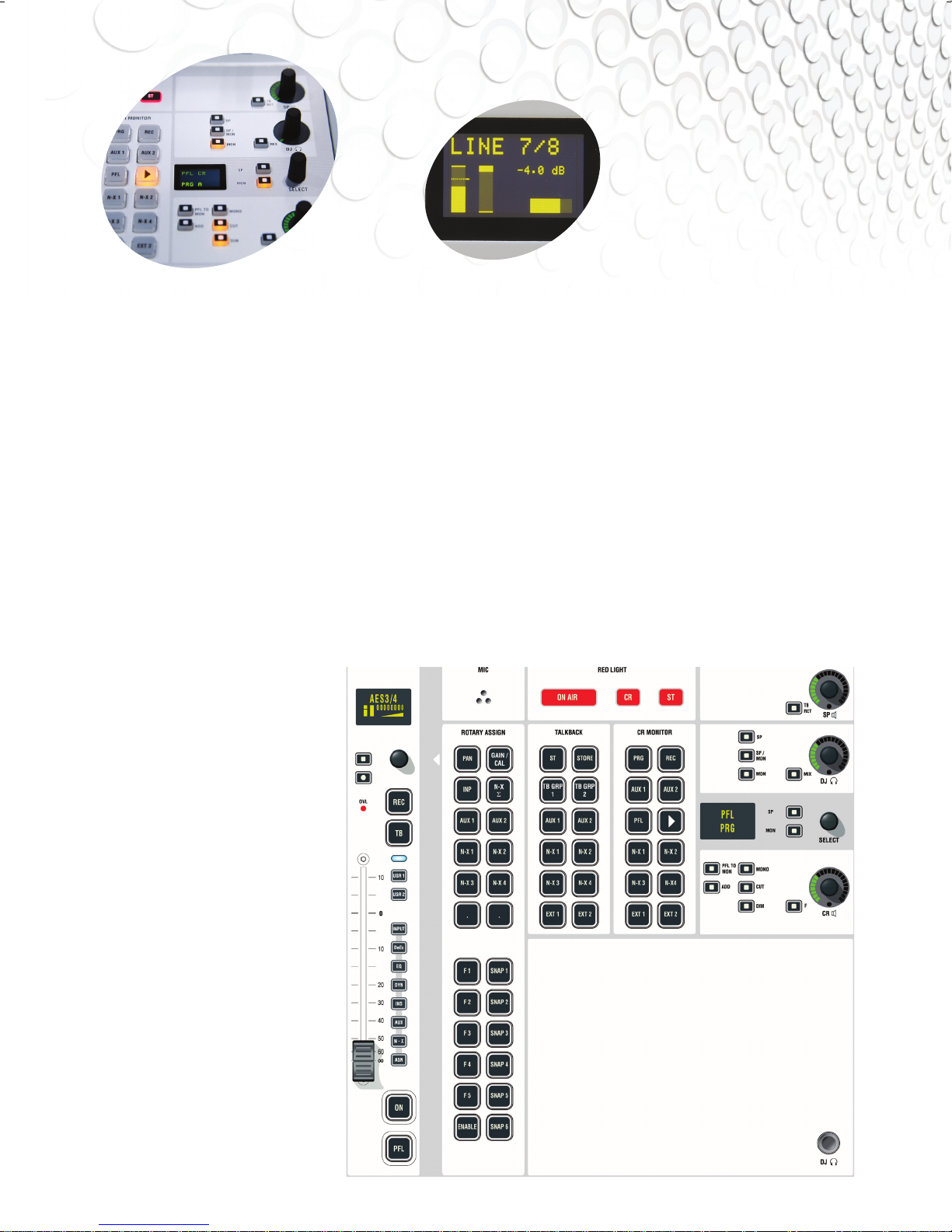
Quick And Intuitive Operation
Like the OnAir 3000, the operation
of the desk is based on Studer’s well
proven and worldwide accepted
“Touch’n’Action” user interface
concept. Within minutes, your talent
is able to operate the console. If your
staff is already experienced with the
OnAir 3000, getting familiar with the
OnAir 2500 is simple. This is ensured
by the clear layout of the user
interface.
Within each single fader strip, an
OLED (Organic LED) ensures
clearest readability of the indicated
information. The display shows the
name of the assigned channel as well
as input level and gain reduction
meters. The level meter can be
alternatively switched to pre or
postfader signal indication or to the
corresponding N-X send level. The
lower right area of the display is
preserved for information about
the function assigned to the rotary
encoder below the display. During
operation, users can choose if the
rotary accesses the channels Gain
setting or the Aux 1 parameters or
any other of the assignable functions.
For immediate visual feedback, the
selected function is always indicated
by an individual graphic icon,
which is supported by text based
parameter indication, whenever the
encoder knob is touched. Two small
pushbuttons allow direct access to
switching parameters, like On/Off or
Pre/Post.
Each faderstrip includes an overload
indication LED which ashes
whenever the channel signal overloads
the input stage. Two large Pushbuttons
with replaceable labels on top of each
fader are precongured as ‘REC’ and
‘TB’. REC routes the channels signal
to the Record Bus, TB allows talkback
into the channel related return line
(available with N-X channel sources).
Below these buttons, a blue LED
indicates an open channel (faderstart
is active). The LED is followed by two
small pushbuttons, which can be
customised. Users can configure the
buttons, for example with a ‘Tally’
function.
On the right hand side of each fader,
a set of eight small pushbuttons with
fixed labels allows direct access to
fader related function pages shown
in the main screen. By pressing the
button at any time, the operator gets
immediate access to the channel
Input page, the DeEsser, EQ,
Dynamics pages, the Insert page or
the Aux, N-X, Bus Assign pages.
A simple touch on the
respective symbol of a channel
function, e.g. equalizer, dynamics,
AUX send, immediately opens the
corresponding page on the main
screen, allowing for quick and easy
adjustment. This can be done either
7
and Ext 1 and 2. The standard
configuration of the console dims the
main speakers whenever a talkback
button is pressed. The internal
microphone represents the default
source for the talkback.
The CR monitoring section provides
the user with a set of sources, which
can be monitored on the control
room speakers or the DJ headphone.
By default, all summing signals, like
Program bus, Record bus, Aux 1 or
2, are directly accessible while other
sources can be selected from a list
using the rotary encoder by the
OLED display. Pressing PFL in a
by the four rotary encoders below
the main screen or directly by
touching a selection list within the
main screen display. To prevent
accidential activation, pushbuttons
and other control elements can be
blocked according to user login rights.
At the bottom of each fader strip, two
large counter-sunk pushbuttons with
replaceable labels are preconfigured
as ‘ON’ and ‘PFL’. While PFL switches
the channels signal to the PFL bus,
ON activates the channel.
The large pushbuttons labelled REC,
TB, ON and PFL can be individually
customised on request. The central
module provides the user with 4
sets of 12 pushbuttons, a monitoring
control section, and an ‘On Air’ and
‘Mic On’ indication for the control
room and the connected studio.
Additionally, this module has an
integrated talkback microphone
and a socket for the DJ headphone
jack.
With the upper left array of 12
pushbuttons, the operator can assign
a function to the fader rotary. In the
standard console layout, the
preconfigured functions to be set are
Pan/Balance, Gain/Calibration,
Input Selection, N-X Send sum, Aux
1, Aux 2 and N-X 1..4 contribution.
In the talkback section, 12
pushbuttons allow communication
with the destination studio, talkback
group 1 and 2, Aux 1 and 2, N-X 1..4
fader strip activates the PFL listening
on the integrated speaker. Volume
for PFL speaker, control room
monitors and DJ headphone can be
controlled by rotary encoders with
value indication.
In the lower left part of the central
module, the fourth 12 pushbutton
array provides a set of user definable
functions. By default, SNAP 1..6 can
be assigned to internal snapshots for
immediate recall of console setups.
All large buttons are equipped with
replaceable key labels. On
request, labels and assigned
functionality can be customised.
8
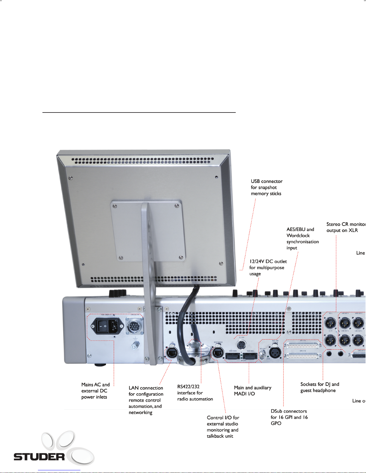
Connectivity
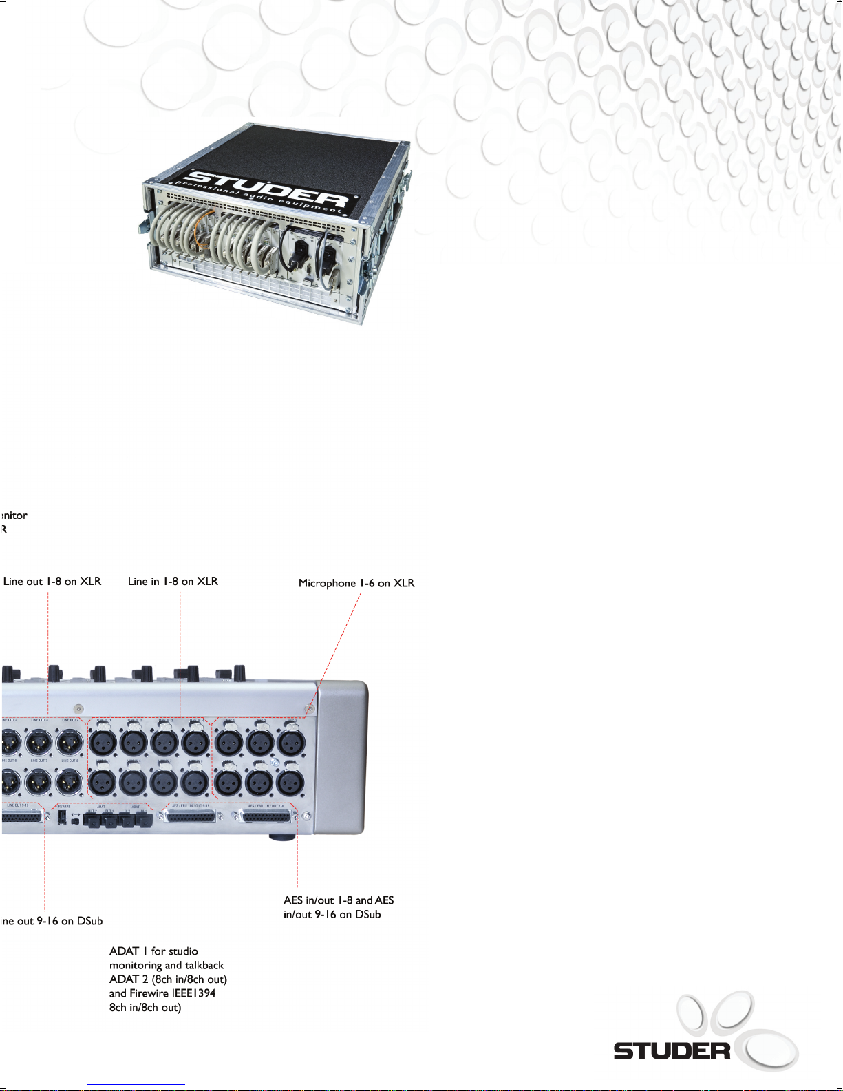
9
Input and output modules
The following D21m input and output cards
are available:
• Microphone / line card, 4
Channels
With analogue insert extension
connector
• Analogue Insert card
Provides 4 balanced insert send and
return paths
• Line In card, 8 channels
24 bit Delta-Sigma A/D converter
card
• Line Out card, 8 channels 24 bit
Delta- Sigma D/A converter card
• AES/EBU card, 8 channels AES/ EBU
in, 8 channels AES/EBU out
Available either with i/p SRC, with i/p
and o/p SRC, or without SRC
• ADAT card, 2 x 8 channels i/p and 2
x 8 channel o/p
With optical interfaces
• TDIF card
Provides 2 TDIF interfaces
• MADI card
Provides optical 64 ch MADI interface
• GPIO card
16 opto-coupler general purpose inputs
16 open collector general purpose
outputs, also available with relays.
The D21m system automatically detects
newly inserted cards in real time and sends
the appropriate information to the main
controller in the OnAir 2500. Additionally,
in the case of a card failure an error
message is transmitted and displayed on
the GUI.
The
OnAir 2500
provides you with an attractive
set of local inputs and outputs in multiple
formats. By connecting a Studer D21m I/O
Breakout box via MADI, the number and
format of the available I/Os can be extended.
10
Radio Integration
With the OnAir 2500, networking
and integration is easy.
Optional support of I/O Sharing
allows Studer’s sophisticated
technology to share signals with other
Studer devices regardless of model. In
a networked installation with multiple
OnAir 2500 and OnAir 3000, Route
6000 and Vista systems, operators
can use I/Os from these systems
and have full access to all parameters
of shared I/Os.
The OnAir 2500 allows integration
with radio automation systems.
Remote control in both directions
from the console to the automation
system and vice versa, is possible via
Monitora option. A single playout
session can be established via serial
interface, while multiple sessions are
possible via TCP/IP. In combination
with the audio connection over
IEEE1394 Firewire with 8ch I/O this
means an effective reduction of
wiring complexity and allows the user
to be on-air ready, fast.
Router control via ProBel is
optionally available. The console is
able to send crosspoint commands to
a Router using the comfortable main
screen as a controller, but it is also
possible to activate output patches in
the router. Patches are sets of
predefined crosspoints, which can be
activated by pressing a single button
on the console surface.
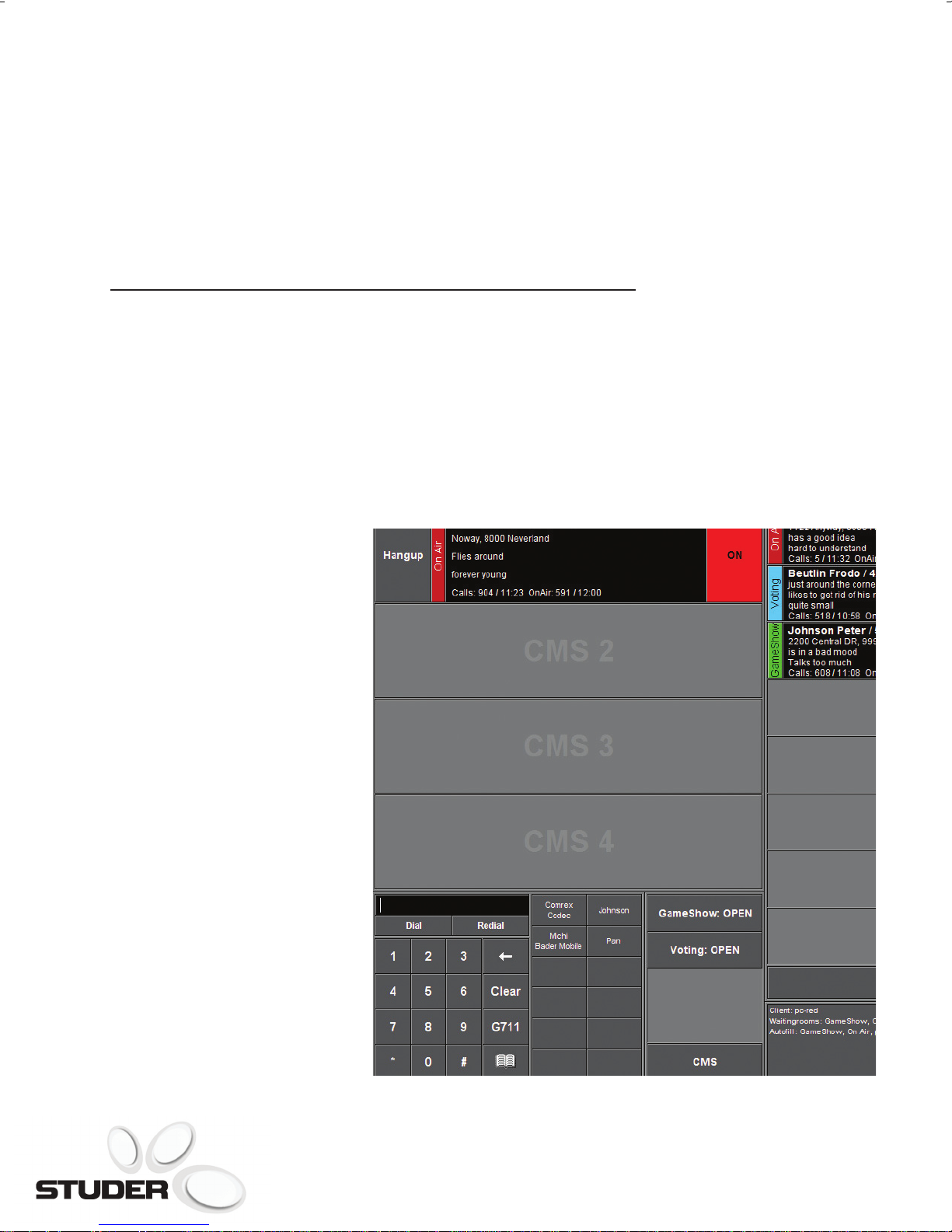
The OnAir 2500 can also be
integrated with Studer’s Call
Management System, CMS. This
system replaces the usual telephone
in a studio by software clients,
allowing sophisticated management
of incoming calls in a networked
environment. The CMS is able to
automatically route incoming callers
to pre-configured fader channels,
allowing caller names to be shown
dynamically as fader channel labels.
Finally, the optional SNMP
functionality enables the system to
send information into the network to
monitor the system’s health. Nearly
any parameter can be selected for
surveillance.

11
OnAir 2500 Main Features:
• Ergonomic, easy to learn “Touch’n’Action” user interface
• Complete system overview and fast parameter access via
fader screens
• 2 master buses PRG A, REC
• 8 weighted stereo mix-minus buses congurable as AUX
sends
• 2 AUX stereo buses
• 8 assignable inserts (stereo) plus analogue mic inserts
• Different audio I/O modules as option by D21m series
extension
• Congurable control signals (GPIOs)
• All buttons freely assignable
• Snapshots, user management, user logins
• Graphical user interface with colour TFT touch screen
• Interface to radio automation system(s)
• Remotely controllable via remote GUI or Probel
protocol
• Redundant power supplies
• Input and output router with graphical display
• Fixed Frame version for easy and fast installation
• Completely adaptable to customer needs
• I/O sharing of audio sources
Inputs
- 6x Mic XLR
- 4x Stereo line XLR
- 8x Stereo AES/EBU with Input SRC on D-Type
- ADAT1 (HCS 200/230μ) (for studio monitoring with 1.943.444 or
1.943.447)
- ADAT2 (POF 980/1000 μ Fiber Wire) or Firewire IEEE-1394
- 1x MADI with 56 IN optical. AUX connector for redundant wiring
- 1x TB mic on desk
Outputs
- 4x Stereo Line XLR
- 4x Stereo Line D-type
- 1x Stereo CR Loudspeaker
- 8x Stereo AES/EBU D-Type
- 1x DJ Headphone (2 connectors)
- 1x GUEST Headphone
- 1x PFL speaker on desk
- 1x ADAT1 (for Studio monitoring)
- 1x ADAT2 or Firewire (IEEE-1394)
- 1x MADI with 40 OUT, AUX connector for redundant wiring
• Each Channel with:
• 4 band parametric EQ
• Limiter, Compressor, Expander, Gate
• De-Esser
• Mic Inputs with High Pass Filter
• One PFL circuit
• Integrated PFL speaker in chassis
• External PFL function (e.g. for playout system)
• Audition bus
• CR monitoring with quick listening function on all inputs
and outputs
• One independent studio monitoring/talkback circuit
• Integrated talkback microphone

12
Technical Specifications
General
Level specs, digital, in dBFS: dB, referenced to full modulation (dBFS, dB Full
Scale)
Level specs, analogue, in dBu: 0 dB Ø 0.775 Vrms
Sampling rate: 48 kHz ±50 ppm (internally synchronized)
Headroom adjustable: 0 to 20 dB
Default setting: 9 dB
Output Level: 15 dBu @ 0 dBFS
All input faders set to their 0 dB position. External analogue sources:
source impedance < 200 Ω. Frequency range: 20 Hz to 20 kHz, if not
stated otherwise.
Microphone inputs
Input sensitivity: –60 dBu…26 dBu for 0 dBFS
Gain setting: in steps of 1dB
Frequency response: 30 Hz…20 kHz, –0.3 dB
High pass lter (12 dB/Octave): 75 Hz
Input impedance: 1.8 kOhm
Insert level (for 0 dBFS) +15 dBu
Dynamic range: 107 dB
THD+N (30 Hz … 20 kHz, –30 dBFS): –100 dBFS
THD+N (1 kHz, –1 dBFS): –95 dBFS
Equivalent input noise (200 Ω Ri, max gain): –124 dBu
Crosstalk, 1 kHz: –100 dB
Phantom power, switchable: 48 V
Line level inputs
Level (for full scale) 15 or 24 dBu xed (jumper), or 7...26 dBu adjustable
Input impedance min. 10 kΩ
Frequency response 20 Hz...20 kHz –0.2 dB
THD & N (35 Hz … 20 kHz, –30 dBFS), input level xed max. –108 dBFS
THD & N (1 kHz, –1 dBFS), input level xed max. –97 dBFS
Crosstalk 1 kHz max. –110 dB
Digital inputs/outputs
Input/Output impedance 110 Ω
Output level (into 110 Ω) 5V
Input Sampling rate with SRC 32 … 108 kHz
Analogue outputs
Level (for full scale) 15 or 24 dBu xed (jumper), or 7 … 26 dBu adjustable
Output Impedance 50 Ω
min. Load at +24 dBu 600 Ω
Frequency response 20 Hz … 20 kHz –0.2 dB
THD & N (20 Hz … 20 kHz, –30 dBFS), input level xed max. –104 dBFS
THD & N (1 kHz, –1 dBFS), input level xed max. –93 dBFS
Crosstalk 1 kHz max. –110 dBFS
Equalizer
4 Band, each band sweepable 20 Hz…20 kHz: ±18 dB
Q-factor 0.27 … 8.7
Dynamics
Dynamic level 0 dB … +24 dB
Dynamics ON/OFF
Limiter
Threshold -39 … + 9dB
Attack time 0.2 msec … 1 msec
Release time 10 msec … 10 sec
Compressor
Threshold -87 … +9 dB
Ratio 20:1 … 1:1
Attack time 0.2 msec … 20 msec
Release time 10 msec … 10 sec
Expander
Threshold -87 … +9 dB
Ratio 20:1 … 1:1
Attack time 0.2 msec … 1 msec
Release time 10 msec … 10 sec
Noise Gate
Threshold -87 … +9 dB
Attenuation -48 dB … 0 dB
Attack time 0.2 msec … 1 msec
Release time 10 msec … 10 sec
De-esser
Frequency range 4 kHz … 14 kHz
Q-factor 0.27 … 8.7
Threshold -87 dB … + 8 dB Auto Mode
Ratio 20:1 … 1:1
Power supply
Mains voltage: 100 to 240 V, 50/60 Hz (auto-ranging)
Power consumption Desk: typ. System 100 W
Weight
OnAir 2500 12 fader 17 kg
Note:
We reserve the right to change specifications as technological progress
may warrant. Data subject to change without notice
13
OnAir 2500 Fixed Frame
Service and Support
Studer has produced and delivered far more than a thousand time-tested and
proven digital OnAir mixing consoles throughout the world, many of which are
in use 24 hours a day, seven days a week. Due to the modular design and the
self-configuring software, individual hardware items can be easily and quickly
exchanged at the customer’s site. We at Studer know that reliability is vital to
our customers. Therefore Studer offers world wide service and support for
its products. Studer also offers operator training and service on-site or in the
factory. Please consult your local Studer representative.


INPUTS INPUT CHANNELS
STEREO INPUT
CHANNEL 1 to n
n = 12/18/24
AES
1/2
3/4
5/6
7/8
9/10
11/12
13/14
15/16
SFC
SFC
SFC
SFC
SFC
SFC
SFC
SFC
D
D
D
D
D
D
D
D
D
D
D
D
D
D
D
D
A
D
MIC
A
D
A
D
A
D
1
2
3
4
A
D
A
D
A
D
5
6
CR
ST
A
D
LINE
A
D
A
D
A
D
3
4
1
2
5
6
7
8
ADAT 2 / IEEE1394
ADAT
1394
D
D
8
d
D
D
8
d
ADAT 1
D
D
8
from
ST
MADI
D
D
56
56
d
d
Alt
GPIN
GPIO
(Optional, in D21m Frame)
16
GPOUT
16
GPIN
GPIO
16
GPOUT
16
#
CR SP SOURCE
CR MON SOURCE
CR MON ADD SOURCE
STUDIO SOURCE
EXT PFL 1
TB from EXT 1...4
TB from CR
TB from STUDIO
TB from EXTERN
EXT PFL 2
CUE
INS RET
CH INP
TEST GEN.
SINE WAVE
WHITE NOISE
PINK NOISE
PHASE
STEREO
CAL
DE-ESSER
INS
PP
PROCESSING
EQ
4-band
DYNAMICS
INS
AP
FADER BALANCE
CHANNEL
ON/OFF
AF
PF
CH METERGR METEROVL
DYNDe-S
PP
AP
4
4
CH
active
AF
PF
PF
AF
CUE
PFL
AF
PF
PF
AF
4
4
TB
TB to CR
TB to CR HP
TB to STUDIO
TB to STUDIO HP
TB to Extern
TB to Ext. 1...4
TB to Int.
1
12
12
AP
PP
CHANNEL OUT
PGM
AUDITION
AUX 1
AUX 2
PFL
REC
N–X 1
N–X
N–X 8
REC PF
INS SEND
+
+
+
+
+
+
+
+
+
+
+
+
CR TB RET
TB to STUDIO TB to STUDIO
TB to
STUDIO HP TB to STUDIO HP
TB to Ext. 1...4
TB to Extern
SLATE/TALK
STUDIO SRC
STUDIO SRC
MASTER / SEND AND MONITORING OUTPUTSS
AUDITION
AUX 1
REC
AUX 2
PFL
PGM
Master AUX Listen
N–X 1
N–X 8
N–X
CUE
N–X
N–X
CUE
CR SRC
CR SP SRC
CR SP SRC
TB to CR HP
CR ADD SRC
TB
TB
PFL
PFL
PFL
PFL
PFL
PFL
REC MASTER
PGM MASTER
AUX 1
AUX 2
SN–X 1
SN–X 8
FADER
FADER
FADER
FADER
FADER
FADER
ON
ON
ON
ON
TB
DIM
TB
DIM
TB
DIM
TB
DIM
TB
DIM
TB
DIM
TALK
TALK
TALK
SLATE
TALK
SLATE
M/S
M/S
INS LIM M/S
INS LIM M/S
M/S
M/S
1/2
3/4
5/6
7/8
9/10
11/12
13/14
15/16
D
D
D
D
D
D
D
D
D
D
D
D
D
D
D
D
AES
D
A
D
A
D
A
D
A
ADAT 2 / IEEE1394
D
D
d
8
D
D
d
8
ADAT 1
D
D
d
8
GUI Meter
MADI
D
D
40
d
4
d
40
Alt
Control
L (M)
R (M)
M
L (M)
R (M)
M
L (M)
R (M)
M
L (M)
R (M)
M
L (M)
R (M)
M
L (M)
R (M)
M
INS SEND
CHANNEL OUT
DIR OUT PP
DIR OUT AP
DJ HP
CR MON SP
GUEST HP
SP
TB to Ext. 1...4
TB to Extern
CR SP
PFL CR
GUEST HP
HP
Audition
#
TB
DIM
CUT
PFL CR
HP Src
CUT
Mono
DIM
TALK
TB
DIM
TB
DIM
CUT
STUDIO
DIM
TALK
TB
DIM
TB
DIM
DIM CUT
Mono
Mono
Mono
TALK
TALK
CR ADD MODE
NONE
SPLIT
MIX
CONTROL ROOM
SP
CR MON
CR/SP
Mono
MON to Left
Mono
with PFL SP
DJ HP MODE
TB
TB
TALK
3
4
2
1
5
6
7
8
D
A
D
A
D
A
D
A
11
12
10
9
13
14
15
16
D
A
D
A
D
A
D
A
DJ HP
CR SP
GUEST HP
SP
SP
HP
GUEST HP
ADAT
1394
LINE
0.9 1.031.05.07/HUR
OnAir 2500
Regensdorf
Switzerland
AUDIO BLOCK
DIAGRAM
SW V3.0
28.04.08/HUR
Configuration C3


Part No. Qt y. Type/Val. DescriptionPos.Idx. Part No. Qt y. Type/Val. DescriptionPos.Idx.
OnAir 2500
Page: 1 of 4
Fader Front PCB 1.943.611.21 ( 0)
C 1 59.60.3337 100n CER 50V, 10%, X7R, 080501 pce
C 2 59.60.3906 47u CER 6.3V, 121001 pce
C 3 not used 10u CER 25V, 121001 pce
C 4 59.60.3337 100n CER 50V, 10%, X7R, 080501 pce
C 5 59.60.3906 47u CER 6.3V, 121001 pce
C 6 59.60.3337 100n CER 50V, 10%, X7R, 080501 pce
C 7 59.60.3906 47u CER 6.3V, 121001 pce
C 8 59.60.3337 100n CER 50V, 10%, X7R, 080501 pce
C 9 59.60.3337 100n CER 50V, 10%, X7R, 080501 pce
C 10 59.60.3337 100n CER 50V, 10%, X7R, 080501 pce
C 11 59.60.3337 100n CER 50V, 10%, X7R, 080501 pce
C 12 59.60.2249 100p CER 50V, 5%, C0G, 060301 pce
C 13 59.60.3337 100n CER 50V, 10%, X7R, 080501 pce
C 14 59.60.3317 2n2 CER 50V, 10%, X7R, 080501 pce
C 15 59.60.3337 100n CER 50V, 10%, X7R, 080501 pce
C 16 59.60.2249 100p CER 50V, 5%, C0G, 060301 pce
C 17 59.60.3317 2n2 CER 50V, 10%, X7R, 080501 pce
C 18 59.60.3337 100n CER 50V, 10%, X7R, 080501 pce
C 19 59.60.3337 100n CER 50V, 10%, X7R, 080501 pce
C 20 59.60.3904 10u CER 6.3V, 080501 pce
C 21 59.60.3337 100n CER 50V, 10%, X7R, 080501 pce
C 22 59.60.3337 100n CER 50V, 10%, X7R, 080501 pce
C 23 59.60.3904 10u CER 6.3V, 080501 pce
C 24 59.60.3337 100n CER 50V, 10%, X7R, 080501 pce
C 25 59.60.3337 100n CER 50V, 10%, X7R, 080501 pce
C 26 59.60.3337 100n CER 50V, 10%, X7R, 080501 pce
C 27 59.60.3904 10u CER 6.3V, 080501 pce
C 28 59.60.3337 100n CER 50V, 10%, X7R, 080501 pce
C 29 59.60.3337 100n CER 50V, 10%, X7R, 080501 pce
C 30 59.60.3904 10u CER 6.3V, 080501 pce
C 31 59.60.3337 100n CER 50V, 10%, X7R, 080501 pce
C 32 59.60.3337 100n CER 50V, 10%, X7R, 080501 pce
C 33 59.60.3904 10u CER 6.3V, 080501 pce
C 34 59.60.3337 100n CER 50V, 10%, X7R, 080501 pce
C 35 59.60.3337 100n CER 50V, 10%, X7R, 080501 pce
C 36 59.60.3904 10u CER 6.3V, 080501 pce
C 37 59.60.3337 100n CER 50V, 10%, X7R, 080501 pce
C 38 59.60.3337 100n CER 50V, 10%, X7R, 080501 pce
C 39 59.60.3337 100n CER 50V, 10%, X7R, 080501 pce
C 40 59.60.3337 100n CER 50V, 10%, X7R, 080501 pce
C 41 59.60.3337 100n CER 50V, 10%, X7R, 080501 pce
C 42 59.60.3337 100n CER 50V, 10%, X7R, 080501 pce
C 43 59.60.3337 100n CER 50V, 10%, X7R, 080501 pce
C 44 59.60.3337 100n CER 50V, 10%, X7R, 080501 pce
C 45 59.60.3337 100n CER 50V, 10%, X7R, 080501 pce
C 46 59.60.3337 100n CER 50V, 10%, X7R, 080501 pce
C 47 59.60.3337 100n CER 50V, 10%, X7R, 080501 pce
C 48 59.60.3337 100n CER 50V, 10%, X7R, 080501 pce
C 49 59.60.3337 100n CER 50V, 10%, X7R, 080501 pce
C 50 59.60.2221 6p8 CER 50V, 5%, C0G, 060301 pce
C 51 59.60.2221 6p8 CER 50V, 5%, C0G, 0603
01 pce
C 52 59.60.2221 6p8 CER 50V, 5%, C0G, 060301 pce
C 53 59.60.2221 6p8 CER 50V, 5%, C0G, 060301 pce
C 54 59.60.3337 100n CER 50V, 10%, X7R, 080501 pce
C 55 59.60.2237 33p CER 50V, 5%, C0G, 060301 pce
C 56 59.60.3321 4n7 CER 50V, 10%, X7R, 080501 pce
C 57 59.60.3321 4n7 CER 50V, 10%, X7R, 080501 pce
C 58 59.60.3321 4n7 CER 50V, 10%, X7R, 080501 pce
C 59 59.60.3321 4n7 CER 50V, 10%, X7R, 080501 pce
C 60 59.60.2237 33p CER 50V, 5%, C0G, 060301 pce
C 61 59.60.3321 4n7 CER 50V, 10%, X7R, 080501 pce
C 62 59.60.3321 4n7 CER 50V, 10%, X7R, 080501 pce
C 63 59.60.3321 4n7 CER 50V, 10%, X7R, 080501 pce
C 64 59.60.3321 4n7 CER 50V, 10%, X7R, 080501 pce
C 65 59.60.3321 4n7 CER 50V, 10%, X7R, 080501 pce
C 66 59.60.3321 4n7 CER 50V, 10%, X7R, 080501 pce
C 67 59.60.3321 4n7 CER 50V, 10%, X7R, 080501 pce
C 68 59.60.3321 4n7 CER 50V, 10%, X7R, 080501 pce
C 69 59.60.3337 100n CER 50V, 10%, X7R, 080501 pce
C 70 59.60.3337 100n CER 50V, 10%, X7R, 080501 pce
C 71 59.60.3337 100n CER 50V, 10%, X7R, 080501 pce
C 72 59.60.3337 100n CER 50V, 10%, X7R, 080501 pce
C 73 59.60.3337 100n CER 50V, 10%, X7R, 080501 pce
C 74 59.60.3337 100n CER 50V, 10%, X7R, 080501 pce
C 75 59.60.3337 100n CER 50V, 10%, X7R, 080501 pce
C 76 59.60.3337 100n CER 50V, 10%, X7R, 080501 pce
C 77 59.60.3337 100n CER 50V, 10%, X7R, 080501 pce
C 78 59.60.3337 100n CER 50V, 10%, X7R, 080501 pce
C 79 59.60.3337 100n CER 50V, 10%, X7R, 080501 pce
C 80 59.60.3337 100n CER 50V, 10%, X7R, 080501 pce
C 81 59.60.3337 100n CER 50V, 10%, X7R, 080501 pce
C 82 59.60.3337 100n CER 50V, 10%, X7R, 080501 pce
C 83 59.60.3337 100n CER 50V, 10%, X7R, 080501 pce
C 84 59.60.3337 100n CER 50V, 10%, X7R, 080501 pce
C 85 59.60.3337 100n CER 50V, 10%, X7R, 080501 pce
C 86 59.60.3337 100n CER 50V, 10%, X7R, 080501 pce
C 87 59.60.3337 100n CER 50V, 10%, X7R, 080501 pce
C 88 59.60.3337 100n CER 50V, 10%, X7R, 080501 pce
C 89 59.60.3337 100n CER 50V, 10%, X7R, 080501 pce
C 90 59.60.3337 100n CER 50V, 10%, X7R, 080501 pce
C 91 59.60.3337 100n CER 50V, 10%, X7R, 080501 pce
C 92 59.60.3337 100n CER 50V, 10%, X7R, 080501 pce
C 93 59.60.3337 100n CER 50V, 10%, X7R, 080501 pce
C 94 59.60.3337 100n CER 50V, 10%, X7R, 080501 pce
C 95 59.60.3337 100n CER 50V, 10%, X7R, 080501 pce
C 96 59.60.3337 100n CER 50V, 10%, X7R, 080501 pce
C 97 59.60.3906 47u CER 6.3V, 121001 pce
C 98 59.60.3906 47u CER 6.3V, 121001 pce
D 1 50.60.8001 4448 200mA 75V 4ns SOD 8001 pce
D 2 50.60.8001 4448 200mA 75V 4ns SOD 8001 pce
D 3 50.60.8901 BAV99 250mA 70V dual SOT 2301 pce
D 4 50.60.8901 BAV99 250mA 70V dual SOT 2301 pce
D 5 50.60.8901 BAV99 250mA 70V dual SOT 2301 pce
D 6 50.60.8901 BAV99 250mA 70V dual SOT 2301 pce
D 7 50.60.8901 BAV99 250mA 70V dual SOT 2301 pce
D 8 50.60.8901 BAV99 250mA 70V dual SOT 2301 pce
D 9 50.60.8001 4448 200mA 75V 4ns SOD 8001 pce
D 10 50.60.8001 4448 200mA 75V 4ns SOD 8001 pce
D 11 50.60.8001 4448 200mA 75V 4ns SOD 8001 pce
D 12 50.60.8001 4448 200mA 75V 4ns SOD 8001 pce
D 13 50.60.8001 4448 200mA 75V 4ns SOD 8001 pce
D 14 50.60.8001 4448 200mA 75V 4ns SOD 8001 pce
D 15 50.60.8001 4448 200mA 75V 4ns SOD 8001 pce
D 16 50.60.8001 4448 200mA 75V 4ns SOD 8001 pce
D 17 50.60.8001 4448 200mA 75V 4ns SOD 8001 pce
D 18 50.60.8001 4448 200mA 75V 4ns SOD 8001 pce
D 19 50.60.8001 4448 200mA 75V 4ns SOD 8001 pce
D 20 50.60.8001 4448 200mA 75V 4ns SOD 8001 pce
D 21 50.60.8001 4448 200mA 75V 4ns SOD 8001 pce
D 22 50.60.8001 4448 200mA 75V 4ns SOD 8001 pce
D 23 50.60.8001 4448 200mA 75V 4ns SOD 8001 pce
D 24 50.60.8001 4448 200mA 75V 4ns SOD 8001 pce
D 25 50.60.8001 4448 200mA 75V 4ns SOD 8001 pce
D 26 50.60.8001 4448 200mA 75V 4ns SOD 8001 pce
D 27 50.60.8001 4448 200mA 75V 4ns SOD 8001 pce
D 28 50.60.8001 4448 200mA 75V 4ns SOD 8001 pce
D 29 50.60.8001 4448 200mA 75V 4ns SOD 8001 pce
D 30 50.60.8001 4448 200mA 75V 4ns SOD 8001 pce
D 31 50.60.8001 4448 200mA 75V 4ns SOD 8001 pce
D 32 50.60.8001 4448 200mA 75V 4ns SOD 8001 pce
D 33 50.60.8001 4448 200mA 75V 4ns SOD 8001 pce
D 34 50.60.8001 4448 200mA 75V 4ns SOD 8001 pce
D 35 50.60.8001 4448 200mA 75V 4ns SOD 8001 pce
D 36 50.60.8001 4448 200mA 75V 4ns SOD 8001 pce
D 37 50.60.8001 4448 200mA 75V 4ns SOD 8001 pce
D 38 50.60.8001 4448 200mA 75V 4ns SOD 8001 pce
D 39 50.60.8001 4448 200mA 75V 4ns SOD 8001 pce
D 40 50.60.8001 4448 200mA 75V 4ns SOD 8001 pce
D 41 50.60.8001 4448 200mA 75V 4ns SOD 8001 pce
D 42 50.60.8001 4448 200mA 75V 4ns SOD 8001 pce
D 43 50.60.8001 4448 200mA 75V 4ns SOD 8001 pce
D 44 50.60.8001 4448 200mA 75V 4ns SOD 8001 pce
D 45 50.60.8001 4448 200mA 75V 4ns SOD 8001 pce
D 46 50.60.8001 4448 200mA 75V 4ns SOD 8001 pce
D 47 50.60.8001 4448 200mA 75V 4ns SOD 8001 pce
D 48 50.60.8001 4448 200mA 75V 4ns SOD 8001 pce
D 49 50.60.8001 4448 200mA 75V 4ns SOD 8001 pce
D 50 50.60.8001 4448 200mA 75V 4ns SOD 8001 pce
D 51 50.60.8001 4448 200mA 75V 4ns SOD 8001 pce
D 52 50.60.8001 4448 200mA 75V 4ns SOD 8001 pce
D 53 50.60.8001 4448 200mA 75V 4ns SOD 8001 pce
D 54 50.60.8001 4448 200mA 75V 4ns SOD 80
01 pce
D 55 50.60.8001 4448 200mA 75V 4ns SOD 8001 pce
D 56 50.60.8001 4448 200mA 75V 4ns SOD 8001 pce
D 57 50.60.8001 4448 200mA 75V 4ns SOD 8001 pce
D 58 50.60.8001 4448 200mA 75V 4ns SOD 8001 pce
D 59 50.60.8001 4448 200mA 75V 4ns SOD 8001 pce
D 60 50.60.8001 4448 200mA 75V 4ns SOD 8001 pce
D 61 50.60.8001 4448 200mA 75V 4ns SOD 8001 pce
D 62 50.60.8001 4448 200mA 75V 4ns SOD 8001 pce
D 63 50.60.8001 4448 200mA 75V 4ns SOD 8001 pce
D 64 50.60.8001 4448 200mA 75V 4ns SOD 8001 pce
D 65 50.60.8001 4448 200mA 75V 4ns SOD 8001 pce
D 66 50.60.8001 4448 200mA 75V 4ns SOD 8001 pce
D 67 50.60.8001 4448 200mA 75V 4ns SOD 8001 pce
D 68 50.60.8001 4448 200mA 75V 4ns SOD 8001 pce
D 69 50.60.8001 4448 200mA 75V 4ns SOD 8001 pce
D 70 50.60.8001 4448 200mA 75V 4ns SOD 8001 pce
D 71 50.60.8001 4448 200mA 75V 4ns SOD 8001 pce
D 72 50.60.8001 4448 200mA 75V 4ns SOD 8001 pce
D 73 50.60.8001 4448 200mA 75V 4ns SOD 8001 pce
D 74 50.60.8001 4448 200mA 75V 4ns SOD 8001 pce
D 75 50.60.8001 4448 200mA 75V 4ns SOD 8001 pce
D 76 50.60.8001 4448 200mA 75V 4ns SOD 8001 pce
D 77 50.60.8001 4448 200mA 75V 4ns SOD 8001 pce
D 78 50.60.8001 4448 200mA 75V 4ns SOD 8001 pce
D 79 50.60.8001 4448 200mA 75V 4ns SOD 8001 pce
D 80 50.60.8001 4448 200mA 75V 4ns SOD 8001 pce
D 81 50.60.8001 4448 200mA 75V 4ns SOD 8001 pce
D 82 50.60.8001 4448 200mA 75V 4ns SOD 8001 pce
D 83 50.60.8001 4448 200mA 75V 4ns SOD 8001 pce
D 84 50.60.8001 4448 200mA 75V 4ns SOD 8001 pce
D 85 50.60.8001 4448 200mA 75V 4ns SOD 8001 pce
D 86 50.60.8001 4448 200mA 75V 4ns SOD 8001 pce
D 87 50.60.8001 4448 200mA 75V 4ns SOD 8001 pce
D 88 50.60.8001 4448 200mA 75V 4ns SOD 8001 pce
D 89 50.60.8001 4448 200mA 75V 4ns SOD 8001 pce
D 90 50.60.8001 4448 200mA 75V 4ns SOD 8001 pce
D 91 50.60.8001 4448 200mA 75V 4ns SOD 8001 pce
D 92 50.60.8001 4448 200mA 75V 4ns SOD 8001 pce
D 93 50.60.8001 4448 200mA 75V 4ns SOD 8001 pce
D 94 50.60.8001 4448 200mA 75V 4ns SOD 8001 pce
D 95 50.60.8001 4448 200mA 75V 4ns SOD 8001 pce
D 96 50.60.8001 4448 200mA 75V 4ns SOD 8001 pce
D 97 50.60.8001 4448 200mA 75V 4ns SOD 8001 pce
D 98 50.60.8001 4448 200mA 75V 4ns SOD 8001 pce
D 99 50.60.8001 4448 200mA 75V 4ns SOD 8001 pce
D 100 50.60.8001 4448 200mA 75V 4ns SOD 8001 pce
D 101 50.60.8001 4448 200mA 75V 4ns SOD 8001 pce
D 102 50.60.8001 4448 200mA 75V 4ns SOD 8001 pce
D 103 50.60.8001 4448 200mA 75V 4ns SOD 8001 pce
D 104 50.60.8001 4448 200mA 75V 4ns SOD 8001 pce
D 105 50.60.8001 4448 200mA 75V 4ns SOD 8001 pce
D 106 50.60.8001 4448 200mA 75V 4ns SOD 8001 pce
D 107 50.60.8001 4448 200mA 75V 4ns SOD 8001 pce
Date printed: 06.06.2008

Part No. Qt y. Type/Val. DescriptionPos.Idx. Part No. Qt y. Type/Val. DescriptionPos.Idx.
OnAir 2500
Page: 2 of 4
Fader Front PCB 1.943.611.21 ( 0)
D 108 50.60.8001 4448 200mA 75V 4ns SOD 8001 pce
D 109 50.60.8001 4448 200mA 75V 4ns SOD 8001 pce
D 110 50.60.8001 4448 200mA 75V 4ns SOD 8001 pce
DL 1 50.60.9402 yel SMD LED yellow01 pce
DL 2 50.60.9402 yel SMD LED yellow01 pce
DL 3 50.60.9402 yel SMD LED yellow01 pce
DL 4 50.60.9402 yel SMD LED yellow01 pce
DL 5 50.60.9402 yel SMD LED yellow01 pce
DL 6 50.60.9402 yel SMD LED yellow01 pce
DL 7 50.60.9402 yel SMD LED yellow01 pce
DL 8 50.60.9402 yel SMD LED yellow01 pce
DL 9 50.60.9402 yel SMD LED yellow01 pce
DL 10 50.60.9402 yel SMD LED yellow01 pce
DL 11 50.60.9402 yel SMD LED yellow01 pce
DL 12 50.60.9402 yel SMD LED yellow01 pce
DL 13 50.60.9402 yel SMD LED yellow01 pce
DL 14 50.60.9401 red SMD LED superred01 pce
DL 15 50.60.9402 yel SMD LED yellow01 pce
DL 16 50.60.9401 red SMD LED superred01 pce
DL 17 50.60.9402 yel SMD LED yellow01 pce
DL 18 50.60.9401 red SMD LED superred01 pce
DL 19 50.60.9402 yel SMD LED yellow01 pce
DL 20 50.60.9401 red SMD LED superred01 pce
DL 21 50.60.9402 yel SMD LED yellow01 pce
DL 22 50.60.9401 red SMD LED superred01 pce
DL 23 50.60.9402 yel SMD LED yellow01 pce
DL 24 50.60.9401 red SMD LED superred01 pce
DL 25 50.60.9401 red SMD LED superred01 pce
DL 26 50.60.9401 red SMD LED superred01 pce
DL 27 50.60.9401 red SMD LED superred01 pce
DL 28 50.60.9401 red SMD LED superred01 pce
DL 29 50.60.9401 red SMD LED superred01 pce
DL 30 50.60.9401 red SMD LED superred01 pce
DL 31 50.60.9402 yel SMD LED yellow01 pce
DL 32 50.60.9401 red SMD LED superred01 pce
DL 33 50.60.9402 yel SMD LED yellow01 pce
DL 34 50.60.9401 red SMD LED superred01 pce
DL 35 50.60.9402 yel SMD LED yellow01 pce
DL 36 50.60.9401 red SMD LED superred01 pce
DL 37 50.60.9402 yel SMD LED yellow01 pce
DL 38 50.60.9401 red SMD LED superred01 pce
DL 39 50.60.9402 yel SMD LED yellow01 pce
DL 40 50.60.9401 red SMD LED superred01 pce
DL 41 50.60.9402 yel SMD LED yellow01 pce
DL 42 50.60.9401 red SMD LED superred01 pce
DL 43 50.60.9418 blu SMD LED 1.25*2.001 pce
DL 44 50.60.9418 blu SMD LED 1.25*2.001 pce
DL 45 50.60.9418 blu SMD LED 1.25*2.001 pce
DL 46 50.60.9418 blu SMD LED 1.25*2.001 pce
DL 47 50.60.9418 blu SMD LED 1.25*2.001 pce
DL 48 50.60.9418 blu SMD LED 1.25*2.0
01 pce
DL 49 50.60.9402 yel SMD LED yellow01 pce
DL 50 50.60.9402 yel SMD LED yellow01 pce
DL 51 50.60.9402 yel SMD LED yellow01 pce
DL 52 50.60.9402 yel SMD LED yellow01 pce
DL 53 50.60.9402 yel SMD LED yellow01 pce
DL 54 50.60.9402 yel SMD LED yellow01 pce
DL 55 50.60.9402 yel SMD LED yellow01 pce
DL 56 50.60.9402 yel SMD LED yellow01 pce
DL 57 50.60.9402 yel SMD LED yellow01 pce
DL 58 50.60.9402 yel SMD LED yellow01 pce
DL 59 50.60.9402 yel SMD LED yellow01 pce
DL 60 50.60.9402 yel SMD LED yellow01 pce
DL 61 50.60.9402 yel SMD LED yellow01 pce
DL 62 50.60.9402 yel SMD LED yellow01 pce
DL 63 50.60.9402 yel SMD LED yellow01 pce
DL 64 50.60.9402 yel SMD LED yellow01 pce
DL 65 50.60.9402 yel SMD LED yellow01 pce
DL 66 50.60.9402 yel SMD LED yellow01 pce
DL 67 50.60.9402 yel SMD LED yellow01 pce
DL 68 50.60.9402 yel SMD LED yellow01 pce
DL 69 50.60.9402 yel SMD LED yellow01 pce
DL 70 50.60.9402 yel SMD LED yellow01 pce
DL 71 50.60.9402 yel SMD LED yellow01 pce
DL 72 50.60.9402 yel SMD LED yellow01 pce
DL 73 50.60.9402 yel SMD LED yellow01 pce
DL 74 50.60.9402 yel SMD LED yellow01 pce
DL 75 50.60.9402 yel SMD LED yellow01 pce
DL 76 50.60.9402 yel SMD LED yellow01 pce
DL 77 50.60.9402 yel SMD LED yellow01 pce
DL 78 50.60.9402 yel SMD LED yellow01 pce
DL 79 50.60.9402 yel SMD LED yellow01 pce
DL 80 50.60.9402 yel SMD LED yellow01 pce
DL 81 50.60.9402 yel SMD LED yellow01 pce
DL 82 50.60.9402 yel SMD LED yellow01 pce
DL 83 50.60.9402 yel SMD LED yellow01 pce
DL 84 50.60.9402 yel SMD LED yellow01 pce
DL 85 50.60.9402 yel SMD LED yellow01 pce
DL 86 50.60.9402 yel SMD LED yellow01 pce
DL 87 50.60.9402 yel SMD LED yellow01 pce
DL 88 50.60.9402 yel SMD LED yellow01 pce
DL 89 50.60.9402 yel SMD LED yellow01 pce
DL 90 50.60.9402 yel SMD LED yellow01 pce
DL 91 50.60.9402 yel SMD LED yellow01 pce
DL 92 50.60.9402 yel SMD LED yellow01 pce
DL 93 50.60.9402 yel SMD LED yellow01 pce
DL 94 50.60.9402 yel SMD LED yellow01 pce
DL 95 50.60.9402 yel SMD LED yellow01 pce
DL 96 50.60.9402 yel SMD LED yellow01 pce
DL 97 50.60.9402 yel SMD LED yellow01 pce
DL 98 50.60.9402 yel SMD LED yellow01 pce
DL 99 50.60.9402 yel SMD LED yellow01 pce
DL 100 50.60.9402 yel SMD LED yellow01 pce
DL 101 50.60.9402 yel SMD LED yellow01 pce
DL 102 50.60.9402 yel SMD LED yellow01 pce
DL 103 50.60.9402 yel SMD LED yellow01 pce
DL 104 50.60.9402 yel SMD LED yellow01 pce
DL 105 50.60.9402 yel SMD LED yellow01 pce
DL 106 50.60.9402 yel SMD LED yellow01 pce
DL 107 50.60.9402 yel SMD LED yellow01 pce
DL 108 50.60.9402 yel SMD LED yellow01 pce
DL 109 50.60.9402 yel SMD LED yellow01 pce
DL 110 50.60.9401 red SMD LED superred01 pce
DL 111 50.60.9402 yel SMD LED yellow01 pce
DL 112 50.60.9401 red SMD LED superred01 pce
DL 113 50.60.9402 yel SMD LED yellow01 pce
DL 114 50.60.9401 red SMD LED superred01 pce
DL 115 50.60.9402 yel SMD LED yellow01 pce
DL 116 50.60.9401 red SMD LED superred01 pce
DL 117 50.60.9402 yel SMD LED yellow01 pce
DL 118 50.60.9401 red SMD LED superred01 pce
DL 119 50.60.9402 yel SMD LED yellow01 pce
DL 120 50.60.9401 red SMD LED superred01 pce
DL 121 50.60.9402 yel SMD LED yellow01 pce
DL 122 50.60.9401 red SMD LED superred01 pce
DL 123 50.60.9402 yel SMD LED yellow01 pce
DL 124 50.60.9401 red SMD LED superred01 pce
DL 125 50.60.9402 yel SMD LED yellow01 pce
DL 126 50.60.9401 red SMD LED superred01 pce
DL 127 50.60.9402 yel SMD LED yellow01 pce
DL 128 50.60.9401 red SMD LED superred01 pce
DL 129 50.60.9402 yel SMD LED yellow01 pce
DL 130 50.60.9401 red SMD LED superred01 pce
DL 131 50.60.9402 yel SMD LED yellow01 pce
DL 132 50.60.9401 red SMD LED superred01 pce
IC 1 1.943.860.20 EPM240 SW611 Rotec8 (50.63.4218)01 pce
IC 2 50.65.0138 74LVC138 3 to 8 line decoder01 pce
IC 3 50.61.0201 TL062 Dual FET Op-Amp01 pce
IC 4 50.65.0244 74LVC244 Octal buffer/line driver 3.3V01 pce
IC 5 50.65.0244 74LVC244 Octal buffer/line driver 3.3V01 pce
IC 6 50.62.1595 74HC595 8bit shift/output register01 pce
IC 7 50.61.9001 LM393 Dual voltage comp. SO 801 pce
IC 8 50.62.1951 74HC4051 8ch analog mux/demux01 pce
IC 9 50.62.1014 74HC 14 Hex Schmitt trigger inverter01 pce
IC 10 50.62.1165 74HC165 8bit shift register01 pce
IC 11 50.62.1165 74HC165 8bit shift register01 pce
IC 12 50.62.1014 74HC 14 Hex Schmitt trigger inverter01 pce
IC 13 50.62.1904 74HCU04 Hex inverter unbuffered01 pce
IC 14 50.62.1595 74HC595 8bit shift/output register01 pce
IC 15 50.62.1595 74HC595 8bit shift/output register
01 pce
IC 16 50.62.1595 74HC595 8bit shift/output register01 pce
IC 17 50.62.1595 74HC595 8bit shift/output register01 pce
IC 18 50.62.1595 74HC595 8bit shift/output register01 pce
IC 19 50.62.1595 74HC595 8bit shift/output register01 pce
IC 20 50.62.1595 74HC595 8bit shift/output register01 pce
IC 21 50.62.1595 74HC595 8bit shift/output register01 pce
IC 22 50.62.1595 74HC595 8bit shift/output register01 pce
IC 23 50.62.1595 74HC595 8bit shift/output register01 pce
IC 24 50.62.1595 74HC595 8bit shift/output register01 pce
IC 25 50.62.1595 74HC595 8bit shift/output register01 pce
IC 26 50.62.1595 74HC595 8bit shift/output register01 pce
IC 27 50.62.1595 74HC595 8bit shift/output register01 pce
IC 28 50.62.1595 74HC595 8bit shift/output register01 pce
IC 29 50.62.1595 74HC595 8bit shift/output register01 pce
IC 30 50.62.1595 74HC595 8bit shift/output register01 pce
MP 1 1.943.611.12 FADERFRONT PCB01 pce
MP 2 1.943.611.10 NR. ETIKETTE 5x2001 pce
MP 3 43.01.0108 Label ESE-Warnschild01 pce
MP 4 1.943.611.01 RUBBER KEY SET01 pce
MP 5 1.943.611.05 OLED SOCKET06 pcs
MP 6 1.943.611.08 OLED 128x64 Dots 1"06 pcs
P 1 54.14.5634 14p PCB-Buchse gerade SMD01 pce
P 2 54.14.5634 14p PCB-Buchse gerade SMD01 pce
P 3 54.14.5630 10p PCB-Buchse gerade SMD01 pce
P 4 54.14.5634 14p PCB-Buchse gerade SMD01 pce
P 5 54.60.0372 26p FFC Connector 0.5mm01 pce
P 6 54.60.0372 26p FFC Connector 0.5mm01 pce
P 7 54.60.0372 26p FFC Connector 0.5mm01 pce
P 8 54.60.0372 26p FFC Connector 0.5mm01 pce
P 9 54.60.0372 26p FFC Connector 0.5mm01 pce
P 10 54.60.0372 26p FFC Connector 0.5mm01 pce
P 11 not us ed 2p Stecker gerade PCB01 pce
P 12 not us ed 2p Stecker gerade PCB01 pce
P 13 not us ed 2p Stecker gerade PCB01 pce
P 14 not us ed 2p Stecker gerade PCB01 pce
P 15 not us ed 2p Stecker gerade PCB01 pce
P 16 not us ed 2p Stecker gerade PCB01 pce
Q 1 50.60.0001 BC847B NPN 45V 100mA SOT 2301 pce
R 1 57.61.1472 4k7 MF, 1%, Chip 0603, E1201 pce
R 2 57.61.1102 1k0 MF, 1%, Chip 0603, E1201 pce
R 3 57.61.1102 1k0 MF, 1%, Chip 0603, E1201 pce
R 4 57.61.1102 1k0 MF, 1%, Chip 0603, E12
01 pce
R 5 57.61.1102 1k0 MF, 1%, Chip 0603, E1201 pce
R 6 57.61.1102 1k0 MF, 1%, Chip 0603, E1201 pce
R 7 57.61.1472 4k7 MF, 1%, Chip 0603, E1201 pce
R 8 57.61.1152 1k5 MF, 1%, Chip 0603, E1201 pce
R 9 57.61.1330 33R MF, 1%, Chip 0603, E1201 pce
R 10 57.61.1332 3k3 MF, 1%, Chip 0603, E1201 pce
R 11 57.61.1152 1k5 MF, 1%, Chip 0603, E1201 pce
R 12 57.61.1330 33R MF, 1%, Chip 0603, E1201 pce
R 13 57.61.1330 33R MF, 1%, Chip 0603, E1201 pce
R 14 57.61.1330 33R MF, 1%, Chip 0603, E1201 pce
R 15 57.61.1102 1k0 MF, 1%, Chip 0603, E1201 pce
R 16 57.61.1330 33R MF, 1%, Chip 0603, E1201 pce
R 17 57.61.1330 33R MF, 1%, Chip 0603, E1201 pce
R 18 57.61.1105 1M0 MF, 1%, Chip 0603, E1201 pce
Date printed: 06.06.2008

Part No. Qt y. Type/Val. DescriptionPos.Idx. Part No. Qt y. Type/Val. DescriptionPos.Idx.
OnAir 2500
Page: 3 of 4
Fader Front PCB 1.943.611.21 ( 0)
R 19 57.61.1330 33R MF, 1%, Chip 0603, E1201 pce
R 20 57.61.1105 1M0 MF, 1%, Chip 0603, E1201 pce
R 21 57.61.1105 1M0 MF, 1%, Chip 0603, E1201 pce
R 22 57.61.1684 680k MF, 1%, Chip 0603, E1201 pce
R 23 57.61.1105 1M0 MF, 1%, Chip 0603, E1201 pce
R 24 57.61.1105 1M0 MF, 1%, Chip 0603, E1201 pce
R 25 57.61.1330 33R MF, 1%, Chip 0603, E1201 pce
R 26 57.61.1330 33R MF, 1%, Chip 0603, E1201 pce
R 27 57.61.1105 1M0 MF, 1%, Chip 0603, E1201 pce
R 28 57.61.1330 33R MF, 1%, Chip 0603, E1201 pce
R 29 57.61.1330 33R MF, 1%, Chip 0603, E1201 pce
R 30 57.61.1102 1k0 MF, 1%, Chip 0603, E1201 pce
R 31 57.61.1563 56k MF, 1%, Chip 0603, E1201 pce
R 32 57.61.1330 33R MF, 1%, Chip 0603, E1201 pce
R 33 57.61.1330 33R MF, 1%, Chip 0603, E1201 pce
R 34 57.61.1104 100k MF, 1%, Chip 0603, E1201 pce
R 35 57.61.1223 22k MF, 1%, Chip 0603, E1201 pce
R 36 57.61.1564 560k MF, 1%, Chip 0603, E1201 pce
R 37 57.61.1123 12k MF, 1%, Chip 0603, E1201 pce
R 38 57.61.1330 33R MF, 1%, Chip 0603, E1201 pce
R 39 57.61.1103 10k MF, 1%, Chip 0603, E1201 pce
R 40 57.61.1330 33R MF, 1%, Chip 0603, E1201 pce
R 41 57.61.1105 1M0 MF, 1%, Chip 0603, E1201 pce
R 42 57.61.1103 10k MF, 1%, Chip 0603, E1201 pce
R 43 57.61.1103 10k MF, 1%, Chip 0603, E1201 pce
R 44 57.61.1330 33R MF, 1%, Chip 0603, E1201 pce
R 45 57.61.1330 33R MF, 1%, Chip 0603, E1201 pce
R 46 57.61.1103 10k MF, 1%, Chip 0603, E1201 pce
R 47 57.61.1472 4k7 MF, 1%, Chip 0603, E1201 pce
R 48 57.61.1104 100k MF, 1%, Chip 0603, E1201 pce
R 49 57.61.1102 1k0 MF, 1%, Chip 0603, E1201 pce
R 50 57.61.1103 10k MF, 1%, Chip 0603, E1201 pce
R 51 57.61.1103 10k MF, 1%, Chip 0603, E1201 pce
R 52 57.61.1103 10k MF, 1%, Chip 0603, E1201 pce
R 53 57.61.1153 15k MF, 1%, Chip 0603, E1201 pce
R 54 57.61.1153 15k MF, 1%, Chip 0603, E1201 pce
R 55 57.61.1105 1M0 MF, 1%, Chip 0603, E1201 pce
R 56 57.61.1105 1M0 MF, 1%, Chip 0603, E1201 pce
R 57 57.61.1103 10k MF, 1%, Chip 0603, E1201 pce
R 58 57.61.1103 10k MF, 1%, Chip 0603, E1201 pce
R 59 57.61.1103 10k MF, 1%, Chip 0603, E1201 pce
R 60 57.61.1103 10k MF, 1%, Chip 0603, E1201 pce
R 61 57.61.1103 10k MF, 1%, Chip 0603, E1201 pce
R 62 57.61.1103 10k MF, 1%, Chip 0603, E1201 pce
R 63 57.61.1103 10k MF, 1%, Chip 0603, E1201 pce
R 64 57.61.1103 10k MF, 1%, Chip 0603, E1201 pce
R 65 57.61.1103 10k MF, 1%, Chip 0603, E1201 pce
R 66 57.61.1102 1k0 MF, 1%, Chip 0603, E1201 pce
R 67 57.61.1102 1k0 MF, 1%, Chip 0603, E1201 pce
R 68 57.61.1102 1k0 MF, 1%, Chip 0603, E1201 pce
R 69 57.61.1102 1k0 MF, 1%, Chip 0603, E12
01 pce
R 70 57.61.1102 1k0 MF, 1%, Chip 0603, E1201 pce
R 71 57.61.1102 1k0 MF, 1%, Chip 0603, E1201 pce
R 72 57.61.1151 150R MF, 1%, Chip 0603, E1201 pce
R 73 57.61.1151 150R MF, 1%, Chip 0603, E1201 pce
R 74 57.61.1151 150R MF, 1%, Chip 0603, E1201 pce
R 75 57.61.1151 150R MF, 1%, Chip 0603, E1201 pce
R 76 57.61.1151 150R MF, 1%, Chip 0603, E1201 pce
R 77 57.61.1151 150R MF, 1%, Chip 0603, E1201 pce
R 78 57.61.1104 100k MF, 1%, Chip 0603, E1201 pce
R 79 57.61.1472 4k7 MF, 1%, Chip 0603, E1201 pce
R 80 57.61.1472 4k7 MF, 1%, Chip 0603, E1201 pce
R 81 57.61.1104 100k MF, 1%, Chip 0603, E1201 pce
R 82 57.61.1101 100R MF, 1%, Chip 0603, E1201 pce
R 83 57.61.1104 100k MF, 1%, Chip 0603, E1201 pce
R 84 57.61.1472 4k7 MF, 1%, Chip 0603, E1201 pce
R 85 57.61.1472 4k7 MF, 1%, Chip 0603, E1201 pce
R 86 57.61.1104 100k MF, 1%, Chip 0603, E1201 pce
R 87 57.61.1104 100k MF, 1%, Chip 0603, E1201 pce
R 88 57.61.1472 4k7 MF, 1%, Chip 0603, E1201 pce
R 89 57.61.1472 4k7 MF, 1%, Chip 0603, E1201 pce
R 90 57.61.1104 100k MF, 1%, Chip 0603, E1201 pce
R 91 57.61.1104 100k MF, 1%, Chip 0603, E1201 pce
R 92 57.61.1472 4k7 MF, 1%, Chip 0603, E1201 pce
R 93 57.61.1472 4k7 MF, 1%, Chip 0603, E1201 pce
R 94 57.61.1104 100k MF, 1%, Chip 0603, E1201 pce
R 95 57.61.1104 100k MF, 1%, Chip 0603, E1201 pce
R 96 57.61.1472 4k7 MF, 1%, Chip 0603, E1201 pce
R 97 57.61.1472 4k7 MF, 1%, Chip 0603, E1201 pce
R 98 57.61.1104 100k MF, 1%, Chip 0603, E1201 pce
R 99 57.61.1104 100k MF, 1%, Chip 0603, E1201 pce
R 100 57.61.1472 4k7 MF, 1%, Chip 0603, E1201 pce
R 101 57.61.1472 4k7 MF, 1%, Chip 0603, E1201 pce
R 102 57.61.1104 100k MF, 1%, Chip 0603, E1201 pce
R 103 57.61.1105 1M0 MF, 1%, Chip 0603, E1201 pce
R 104 57.61.1151 150R MF, 1%, Chip 0603, E1201 pce
R 105 57.61.1151 150R MF, 1%, Chip 0603, E1201 pce
R 106 57.61.1151 150R MF, 1%, Chip 0603, E1201 pce
R 107 57.61.1151 150R MF, 1%, Chip 0603, E1201 pce
R 108 57.61.1151 150R MF, 1%, Chip 0603, E1201 pce
R 109 57.61.1151 150R MF, 1%, Chip 0603, E1201 pce
R 110 57.61.1151 150R MF, 1%, Chip 0603, E1201 pce
R 111 57.61.1151 150R MF, 1%, Chip 0603, E1201 pce
R 112 57.61.1151 150R MF, 1%, Chip 0603, E1201 pce
R 113 57.61.1151 150R MF, 1%, Chip 0603, E1201 pce
R 114 57.61.1121 120R MF, 1%, Chip 0603, E1201 pce
R 115 57.61.1151 150R MF, 1%, Chip 0603, E1201 pce
R 116 57.61.1121 120R MF, 1%, Chip 0603, E1201 pce
R 117 57.61.1151 150R MF, 1%, Chip 0603, E1201 pce
R 118 57.61.1121 120R MF, 1%, Chip 0603, E1201 pce
R 119 57.61.1151 150R MF, 1%, Chip 0603, E1201 pce
R 120 57.61.1121 120R MF, 1%, Chip 0603, E1201 pce
R 121 57.61.1151 150R MF, 1%, Chip 0603, E1201 pce
R 122 57.61.1121 120R MF, 1%, Chip 0603, E1201 pce
R 123 57.61.1151 150R MF, 1%, Chip 0603, E1201 pce
R 124 57.61.1121 120R MF, 1%, Chip 0603, E1201 pce
R 125 57.61.1151 150R MF, 1%, Chip 0603, E1201 pce
R 126 57.61.1151 150R MF, 1%, Chip 0603, E1201 pce
R 127 57.61.1151 150R MF, 1%, Chip 0603, E1201 pce
R 128 57.61.1151 150R MF, 1%, Chip 0603, E1201 pce
R 129 57.61.1121 120R MF, 1%, Chip 0603, E1201 pce
R 130 57.61.1151 150R MF, 1%, Chip 0603, E1201 pce
R 131 57.61.1121 120R MF, 1%, Chip 0603, E1201 pce
R 132 57.61.1151 150R MF, 1%, Chip 0603, E1201 pce
R 133 57.61.1121 120R MF, 1%, Chip 0603, E1201 pce
R 134 57.61.1151 150R MF, 1%, Chip 0603, E1201 pce
R 135 57.61.1121 120R MF, 1%, Chip 0603, E1201 pce
R 136 57.61.1151 150R MF, 1%, Chip 0603, E1201 pce
R 137 57.61.1121 120R MF, 1%, Chip 0603, E1201 pce
R 138 57.61.1151 150R MF, 1%, Chip 0603, E1201 pce
R 139 57.61.1121 120R MF, 1%, Chip 0603, E1201 pce
R 140 57.61.1101 100R MF, 1%, Chip 0603, E1201 pce
R 141 57.61.1101 100R MF, 1%, Chip 0603, E1201 pce
R 142 57.61.1101 100R MF, 1%, Chip 0603, E1201 pce
R 143 57.61.1101 100R MF, 1%, Chip 0603, E1201 pce
R 144 57.61.1101 100R MF, 1%, Chip 0603, E1201 pce
R 145 57.61.1101 100R MF, 1%, Chip 0603, E1201 pce
R 146 57.61.1151 150R MF, 1%, Chip 0603, E1201 pce
R 147 57.61.1151 150R MF, 1%, Chip 0603, E1201 pce
R 148 57.61.1151 150R MF, 1%, Chip 0603, E1201 pce
R 149 57.61.1151 150R MF, 1%, Chip 0603, E1201 pce
R 150 57.61.1151 150R MF, 1%, Chip 0603, E1201 pce
R 151 57.61.1151 150R MF, 1%, Chip 0603, E1201 pce
R 152 57.61.1151 150R MF, 1%, Chip 0603, E1201 pce
R 153 57.61.1151 150R MF, 1%, Chip 0603, E1201 pce
R 154 57.61.1151 150R MF, 1%, Chip 0603, E1201 pce
R 155 57.61.1151 150R MF, 1%, Chip 0603, E1201 pce
R 156 57.61.1151 150R MF, 1%, Chip 0603, E1201 pce
R 157 57.61.1151 150R MF, 1%, Chip 0603, E1201 pce
R 158 57.61.1151 150R MF, 1%, Chip 0603, E1201 pce
R 159 57.61.1151 150R MF, 1%, Chip 0603, E1201 pce
R 160 57.61.1151 150R MF, 1%, Chip 0603, E1201 pce
R 161 57.61.1151 150R MF, 1%, Chip 0603, E1201 pce
R 162 57.61.1151 150R MF, 1%, Chip 0603, E1201 pce
R 163 57.61.1151 150R MF, 1%, Chip 0603, E1201 pce
R 164 57.61.1151 150R MF, 1%, Chip 0603, E1201 pce
R 165 57.61.1151 150R MF, 1%, Chip 0603, E1201 pce
R 166 57.61.1151 150R MF, 1%, Chip 0603, E1201 pce
R 167 57.61.1151 150R MF, 1%, Chip 0603, E1201 pce
R 168 57.61.1151 150R MF, 1%, Chip 0603, E1201 pce
R 169 57.61.1151 150R MF, 1%, Chip 0603, E1201 pce
R 170 57.61.1151 150R MF, 1%, Chip 0603, E12
01 pce
R 171 57.61.1151 150R MF, 1%, Chip 0603, E1201 pce
R 172 57.61.1151 150R MF, 1%, Chip 0603, E1201 pce
R 173 57.61.1151 150R MF, 1%, Chip 0603, E1201 pce
R 174 57.61.1151 150R MF, 1%, Chip 0603, E1201 pce
R 175 57.61.1151 150R MF, 1%, Chip 0603, E1201 pce
R 176 57.61.1151 150R MF, 1%, Chip 0603, E1201 pce
R 177 57.61.1151 150R MF, 1%, Chip 0603, E1201 pce
R 178 57.61.1151 150R MF, 1%, Chip 0603, E1201 pce
R 179 57.61.1151 150R MF, 1%, Chip 0603, E1201 pce
R 180 57.61.1151 150R MF, 1%, Chip 0603, E1201 pce
R 181 57.61.1151 150R MF, 1%, Chip 0603, E1201 pce
R 182 57.61.1151 150R MF, 1%, Chip 0603, E1201 pce
R 183 57.61.1151 150R MF, 1%, Chip 0603, E1201 pce
R 184 57.61.1151 150R MF, 1%, Chip 0603, E1201 pce
R 185 57.61.1151 150R MF, 1%, Chip 0603, E1201 pce
R 186 57.61.1151 150R MF, 1%, Chip 0603, E1201 pce
R 187 57.61.1151 150R MF, 1%, Chip 0603, E1201 pce
R 188 57.61.1151 150R MF, 1%, Chip 0603, E1201 pce
R 189 57.61.1151 150R MF, 1%, Chip 0603, E1201 pce
R 190 57.61.1151 150R MF, 1%, Chip 0603, E1201 pce
R 191 57.61.1151 150R MF, 1%, Chip 0603, E1201 pce
R 192 57.61.1151 150R MF, 1%, Chip 0603, E1201 pce
R 193 57.61.1151 150R MF, 1%, Chip 0603, E1201 pce
R 194 57.61.1151 150R MF, 1%, Chip 0603, E1201 pce
R 195 57.61.1151 150R MF, 1%, Chip 0603, E1201 pce
R 196 57.61.1151 150R MF, 1%, Chip 0603, E1201 pce
R 197 57.61.1151 150R MF, 1%, Chip 0603, E1201 pce
R 198 57.61.1151 150R MF, 1%, Chip 0603, E1201 pce
R 199 57.61.1151 150R MF, 1%, Chip 0603, E1201 pce
R 200 57.61.1151 150R MF, 1%, Chip 0603, E1201 pce
R 201 57.61.1151 150R MF, 1%, Chip 0603, E1201 pce
R 202 57.61.1151 150R MF, 1%, Chip 0603, E1201 pce
R 203 57.61.1151 150R MF, 1%, Chip 0603, E1201 pce
R 204 57.61.1151 150R MF, 1%, Chip 0603, E1201 pce
R 205 57.61.1151 150R MF, 1%, Chip 0603, E1201 pce
R 206 57.61.1151 150R MF, 1%, Chip 0603, E1201 pce
R 207 57.61.1121 120R MF, 1%, Chip 0603, E1201 pce
R 208 57.61.1151 150R MF, 1%, Chip 0603, E1201 pce
R 209 57.61.1121 120R MF, 1%, Chip 0603, E1201 pce
R 210 57.61.1151 150R MF, 1%, Chip 0603, E1201 pce
R 211 57.61.1121 120R MF, 1%, Chip 0603, E1201 pce
R 212 57.61.1151 150R MF, 1%, Chip 0603, E1201 pce
R 213 57.61.1121 120R MF, 1%, Chip 0603, E1201 pce
R 214 57.61.1151 150R MF, 1%, Chip 0603, E1201 pce
R 215 57.61.1121 120R MF, 1%, Chip 0603, E1201 pce
R 216 57.61.1151 150R MF, 1%, Chip 0603, E1201 pce
R 217 57.61.1121 120R MF, 1%, Chip 0603, E1201 pce
R 218 57.61.1151 150R MF, 1%, Chip 0603, E1201 pce
R 219 57.61.1121 120R MF, 1%, Chip 0603, E1201 pce
R 220 57.61.1151 150R MF, 1%, Chip 0603, E1201 pce
R 221 57.61.1121 120R MF, 1%, Chip 0603, E1201 pce
R 222 57.61.1151 150R MF, 1%, Chip 0603, E1201 pce
R 223 57.61.1121 120R MF, 1%, Chip 0603, E1201 pce
R 224 57.61.1151 150R MF, 1%, Chip 0603, E1201 pce
Date printed: 06.06.2008

Part No. Qt y. Type/Val. DescriptionPos.Idx. Part No. Qt y. Type/Val. DescriptionPos.Idx.
OnAir 2500
Page: 4 of 4
Fader Front PCB 1.943.611.21 ( 0)
R 225 57.61.1121 120R MF, 1%, Chip 0603, E1201 pce
R 226 57.61.1151 150R MF, 1%, Chip 0603, E1201 pce
R 227 57.61.1121 120R MF, 1%, Chip 0603, E1201 pce
R 228 57.61.1151 150R MF, 1%, Chip 0603, E1201 pce
R 229 57.61.1121 120R MF, 1%, Chip 0603, E1201 pce
S 7 55.12.1304 N=18 Encoder01 pce
S 8 55.12.1304 N=18 Encoder01 pce
S 9 55.12.1304 N=18 Encoder01 pce
S 10 55.12.1304 N=18 Encoder01 pce
S 11 55.12.1304 N=18 Encoder01 pce
S 12 55.12.1304 N=18 Encoder01 pce
Y 1 89.60.1011 6.000MHz SMD Quartz01 pce
End of List
[21] 14.03.2008 ZT release
Date printed: 06.06.2008


Part No. Qt y. Type/Val. DescriptionPos.Idx. Part No. Qt y. Type/Val. DescriptionPos.Idx.
OnAir 2500
Page: 1 of 4
Fader Control PCB 1.943.612.22 ( 0)
C 1 59.60.3337 100n CER 50V, 10%, X7R, 080501 pce
C 2 59.60.3906 47u CER 6.3V, 121001 pce
C 3 59.60.3337 100n CER 50V, 10%, X7R, 080501 pce
C 4 59.60.3904 10u CER 6.3V, 080501 pce
C 5 59.60.3337 100n CER 50V, 10%, X7R, 080501 pce
C 6 59.60.3906 47u CER 6.3V, 121001 pce
C 7 59.60.3906 47u CER 6.3V, 121001 pce
C 8 59.68.0067 22u EL 16V, 5.0*5.701 pce
C 9 59.60.3906 47u CER 6.3V, 121001 pce
C 10 59.60.3337 100n CER 50V, 10%, X7R, 080501 pce
C 11 59.60.3337 100n CER 50V, 10%, X7R, 080501 pce
C 12 59.60.3906 47u CER 6.3V, 121001 pce
C 13 59.60.3337 100n CER 50V, 10%, X7R, 080501 pce
C 14 59.60.3337 100n CER 50V, 10%, X7R, 080501 pce
C 15 59.60.3337 100n CER 50V, 10%, X7R, 080501 pce
C 16 59.60.3337 100n CER 50V, 10%, X7R, 080501 pce
C 17 59.60.3904 10u CER 6.3V, 080501 pce
C 18 59.60.3903 1u0 CER 6.3V, 060301 pce
C 19 59.60.3337 100n CER 50V, 10%, X7R, 080501 pce
C 20 59.60.2373 1n0 CER 50V, 5%, C0G, 080501 pce
C 21 59.60.3337 100n CER 50V, 10%, X7R, 080501 pce
C 22 not used 10u CER 25V, 121001 pce
C 23 59.60.3337 100n CER 50V, 10%, X7R, 080501 pce
C 24 59.60.3903 1u0 CER 6.3V, 060301 pce
C 25 59.60.3903 1u0 CER 6.3V, 060301 pce
C 26 59.60.3903 1u0 CER 6.3V, 060301 pce
C 27 59.60.2349 100p CER 50V, 5%, C0G, 080501 pce
C 28 59.60.3337 100n CER 50V, 10%, X7R, 080501 pce
C 29 59.60.3905 10u CER 25V, 121001 pce
C 30 59.60.3903 1u0 CER 6.3V, 060301 pce
C 31 59.60.3903 1u0 CER 6.3V, 060301 pce
C 32 59.60.3904 10u CER 6.3V, 080501 pce
C 33 59.60.3905 10u CER 25V, 121001 pce
C 34 59.60.3902 100n CER 6.3V, 040201 pce
C 35 59.60.3337 100n CER 50V, 10%, X7R, 080501 pce
C 36 59.60.3903 1u0 CER 6.3V, 060301 pce
C 37 59.60.3903 1u0 CER 6.3V, 060301 pce
C 38 59.60.3333 47n CER 50V, 10%, X7R, 080501 pce
C 39 59.60.3337 100n CER 50V, 10%, X7R, 080501 pce
C 40 59.60.3333 47n CER 50V, 10%, X7R, 080501 pce
C 41 59.60.3337 100n CER 50V, 10%, X7R, 080501 pce
C 42 59.60.2363 390p CER 50V, 5%, C0G, 080501 pce
C 43 59.60.3902 100n CER 6.3V, 040201 pce
C 44 59.60.3333 47n CER 50V, 10%, X7R, 080501 pce
C 45 59.60.3337 100n CER 50V, 10%, X7R, 080501 pce
C 46 59.60.3337 100n CER 50V, 10%, X7R, 080501 pce
C 47 59.60.3337 100n CER 50V, 10%, X7R, 080501 pce
C 48 59.60.3904 10u CER 6.3V, 080501 pce
C 49 59.60.3904 10u CER 6.3V, 080501 pce
C 50 59.60.3337 100n CER 50V, 10%, X7R, 080501 pce
C 51 59.60.3905 10u CER 25V, 1210
01 pce
C 52 59.60.3325 10n CER 50V, 10%, X7R, 080501 pce
C 53 59.60.3902 100n CER 6.3V, 040201 pce
C 54 59.60.3902 100n CER 6.3V, 040201 pce
C 55 59.60.2249 100p CER 50V, 5%, C0G, 060301 pce
C 56 59.60.3902 100n CER 6.3V, 040201 pce
C 57 59.60.3321 4n7 CER 50V, 10%, X7R, 080501 pce
C 58 59.60.3337 100n CER 50V, 10%, X7R, 080501 pce
C 59 59.60.3905 10u CER 25V, 121001 pce
C 60 59.60.3337 100n CER 50V, 10%, X7R, 080501 pce
C 61 59.60.3902 100n CER 6.3V, 040201 pce
C 62 59.60.3321 4n7 CER 50V, 10%, X7R, 080501 pce
C 63 59.60.3337 100n CER 50V, 10%, X7R, 080501 pce
C 64 59.60.3333 47n CER 50V, 10%, X7R, 080501 pce
C 65 59.60.3321 4n7 CER 50V, 10%, X7R, 080501 pce
C 66 59.60.3337 100n CER 50V, 10%, X7R, 080501 pce
C 67 59.60.3333 47n CER 50V, 10%, X7R, 080501 pce
C 68 59.60.3337 100n CER 50V, 10%, X7R, 080501 pce
C 69 59.60.3333 47n CER 50V, 10%, X7R, 080501 pce
C 70 59.60.3321 4n7 CER 50V, 10%, X7R, 080501 pce
C 71 59.60.3337 100n CER 50V, 10%, X7R, 080501 pce
C 72 59.60.3337 100n CER 50V, 10%, X7R, 080501 pce
C 73 59.60.3337 100n CER 50V, 10%, X7R, 080501 pce
C 74 59.60.3902 100n CER 6.3V, 040201 pce
C 75 59.60.3321 4n7 CER 50V, 10%, X7R, 080501 pce
C 76 59.60.3337 100n CER 50V, 10%, X7R, 080501 pce
C 77 59.60.3333 47n CER 50V, 10%, X7R, 080501 pce
C 78 59.60.3337 100n CER 50V, 10%, X7R, 080501 pce
C 79 59.60.3333 47n CER 50V, 10%, X7R, 080501 pce
C 80 59.60.3337 100n CER 50V, 10%, X7R, 080501 pce
C 81 59.60.3337 100n CER 50V, 10%, X7R, 080501 pce
C 82 59.60.3317 2n2 CER 50V, 10%, X7R, 080501 pce
C 83 59.60.3337 100n CER 50V, 10%, X7R, 080501 pce
C 84 59.60.3317 2n2 CER 50V, 10%, X7R, 080501 pce
C 85 59.60.3317 2n2 CER 50V, 10%, X7R, 080501 pce
C 86 59.60.3905 10u CER 25V, 121001 pce
C 87 59.60.3317 2n2 CER 50V, 10%, X7R, 080501 pce
C 88 59.60.3337 100n CER 50V, 10%, X7R, 080501 pce
C 89 59.60.3317 2n2 CER 50V, 10%, X7R, 080501 pce
C 90 59.60.3321 4n7 CER 50V, 10%, X7R, 080501 pce
C 91 59.60.3904 10u CER 6.3V, 080501 pce
C 92 59.60.3337 100n CER 50V, 10%, X7R, 080501 pce
C 93 59.60.3317 2n2 CER 50V, 10%, X7R, 080501 pce
C 94 59.60.3337 100n CER 50V, 10%, X7R, 080501 pce
C 95 59.60.3329 22n CER 50V, 10%, X7R, 080501 pce
C 96 59.60.3333 47n CER 50V, 10%, X7R, 080501 pce
C 97 59.60.3337 100n CER 50V, 10%, X7R, 080501 pce
C 98 59.60.3329 22n CER 50V, 10%, X7R, 080501 pce
C 99 59.60.3329 22n CER 50V, 10%, X7R, 080501 pce
C 100 59.60.3333 47n CER 50V, 10%, X7R, 080501 pce
C 101 59.60.3902 100n CER 6.3V, 040201 pce
C 102 59.60.3902 100n CER 6.3V, 040201 pce
C 103 59.60.3905 10u CER 25V, 121001 pce
C 104 59.60.2257 220p CER 50V, 5%, C0G, 060301 pce
C 105 59.60.3329 22n CER 50V, 10%, X7R, 080501 pce
C 106 59.60.3333 47n CER 50V, 10%, X7R, 080501 pce
C 107 59.60.3337 100n CER 50V, 10%, X7R, 080501 pce
C 108 59.60.3329 22n CER 50V, 10%, X7R, 080501 pce
C 109 59.60.3329 22n CER 50V, 10%, X7R, 080501 pce
C 110 59.60.3333 47n CER 50V, 10%, X7R, 080501 pce
C 111 59.60.3337 100n CER 50V, 10%, X7R, 080501 pce
C 112 59.60.2233 22p CER 50V, 5%, C0G, 060301 pce
C 113 59.60.2233 22p CER 50V, 5%, C0G, 060301 pce
C 114 59.60.2361 330p CER 50V, 5%, C0G, 080501 pce
C 115 59.60.3337 100n CER 50V, 10%, X7R, 080501 pce
C 116 59.60.2361 330p CER 50V, 5%, C0G, 080501 pce
C 117 59.60.3337 100n CER 50V, 10%, X7R, 080501 pce
C 118 59.60.2361 330p CER 50V, 5%, C0G, 080501 pce
C 119 59.60.3337 100n CER 50V, 10%, X7R, 080501 pce
C 120 59.60.3906 47u CER 6.3V, 121001 pce
C 121 59.60.3337 100n CER 50V, 10%, X7R, 080501 pce
C 122 59.60.3337 100n CER 50V, 10%, X7R, 080501 pce
C 123 59.60.3337 100n CER 50V, 10%, X7R, 080501 pce
C 124 59.60.2361 330p CER 50V, 5%, C0G, 080501 pce
C 125 59.60.3337 100n CER 50V, 10%, X7R, 080501 pce
C 126 59.60.2361 330p CER 50V, 5%, C0G, 080501 pce
C 127 59.60.3337 100n CER 50V, 10%, X7R, 080501 pce
C 128 59.60.2361 330p CER 50V, 5%, C0G, 080501 pce
C 129 59.60.3337 100n CER 50V, 10%, X7R, 080501 pce
C 130 59.60.3337 100n CER 50V, 10%, X7R, 080501 pce
C 131 59.60.3337 100n CER 50V, 10%, X7R, 080501 pce
C 132 59.60.3337 100n CER 50V, 10%, X7R, 080501 pce
C 133 59.60.3906 47u CER 6.3V, 121001 pce
C 134 59.60.3904 10u CER 6.3V, 080501 pce
C 135 59.60.3904 10u CER 6.3V, 080501 pce
C 136 59.60.3337 100n CER 50V, 10%, X7R, 080501 pce
C 137 59.60.3337 100n CER 50V, 10%, X7R, 080501 pce
C 138 59.60.3337 100n CER 50V, 10%, X7R, 080501 pce
C 139 59.68.0317 220u EL 35V, 10 *10.7 lowESR01 pce
C 140 59.60.3337 100n CER 50V, 10%, X7R, 080501 pce
C 141 59.60.3905 10u CER 25V, 121001 pce
C 142 59.60.3905 10u CER 25V, 121001 pce
C 143 not used 10u CER 25V, 121001 pce
C 144 59.60.3325 10n CER 50V, 10%, X7R, 080501 pce
C 145 59.60.3337 100n CER 50V, 10%, X7R, 080501 pce
C 146 59.68.0275 470u EL 16V, 10 *10.7 lowESR01 pce
C 147 59.68.0275 470u EL 16V, 10 *10.7 lowESR01 pce
C 148 59.68.0317 220u EL 35V, 10 *10.7 lowESR01 pce
C 149 59.60.3905 10u CER 25V, 121001 pce
C 150 59.60.3337 100n CER 50V, 10%, X7R, 080501 pce
C 151 59.60.3337 100n CER 50V, 10%, X7R, 080501 pce
C 152 59.60.3337 100n CER 50V, 10%, X7R, 0805
01 pce
C 153 59.60.3337 100n CER 50V, 10%, X7R, 080501 pce
C 154 59.60.3337 100n CER 50V, 10%, X7R, 080501 pce
C 155 59.60.3337 100n CER 50V, 10%, X7R, 080501 pce
C 156 59.60.3337 100n CER 50V, 10%, X7R, 080501 pce
C 157 59.68.0109 10u EL 35V, 5.0*5.701 pce
C 158 59.60.3337 100n CER 50V, 10%, X7R, 080501 pce
C 159 59.60.2373 1n0 CER 50V, 5%, C0G, 080501 pce
C 160 59.60.3337 100n CER 50V, 10%, X7R, 080501 pce
C 161 59.60.2373 1n0 CER 50V, 5%, C0G, 080501 pce
C 162 59.60.2373 1n0 CER 50V, 5%, C0G, 080501 pce
C 163 59.60.3337 100n CER 50V, 10%, X7R, 080501 pce
C 164 59.60.3337 100n CER 50V, 10%, X7R, 080501 pce
C 165 59.60.3325 10n CER 50V, 10%, X7R, 080501 pce
C 166 59.60.3325 10n CER 50V, 10%, X7R, 080501 pce
C 167 59.60.2373 1n0 CER 50V, 5%, C0G, 080501 pce
C 168 59.60.3325 10n CER 50V, 10%, X7R, 080501 pce
C 169 59.60.2373 1n0 CER 50V, 5%, C0G, 080501 pce
C 170 59.60.2373 1n0 CER 50V, 5%, C0G, 080501 pce
C 171 59.60.2249 100p CER 50V, 5%, C0G, 060301 pce
C 172 59.60.2249 100p CER 50V, 5%, C0G, 060301 pce
C 173 59.60.3325 10n CER 50V, 10%, X7R, 080501 pce
C 174 59.60.2249 100p CER 50V, 5%, C0G, 060301 pce
C 175 59.60.3325 10n CER 50V, 10%, X7R, 080501 pce
C 176 59.60.3325 10n CER 50V, 10%, X7R, 080501 pce
C 177 59.60.2249 100p CER 50V, 5%, C0G, 060301 pce
C 178 59.60.2249 100p CER 50V, 5%, C0G, 060301 pce
C 179 59.60.2249 100p CER 50V, 5%, C0G, 060301 pce
C 180 59.60.3337 100n CER 50V, 10%, X7R, 080501 pce
C 181 59.60.3337 100n CER 50V, 10%, X7R, 080501 pce
C 182 59.60.3337 100n CER 50V, 10%, X7R, 080501 pce
C 183 59.60.3337 100n CER 50V, 10%, X7R, 080501 pce
C 184 59.60.3337 100n CER 50V, 10%, X7R, 080501 pce
C 185 59.60.3337 100n CER 50V, 10%, X7R, 080501 pce
C 186 59.60.3337 100n CER 50V, 10%, X7R, 080501 pce
C 187 59.60.3333 47n CER 50V, 10%, X7R, 080501 pce
C 188 59.60.3333 47n CER 50V, 10%, X7R, 080501 pce
C 189 59.60.3333 47n CER 50V, 10%, X7R, 080501 pce
C 190 59.68.0109 10u EL 35V, 5.0*5.701 pce
C 191 59.60.3333 47n CER 50V, 10%, X7R, 080501 pce
C 192 59.60.3337 100n CER 50V, 10%, X7R, 080501 pce
C 193 59.60.3333 47n CER 50V, 10%, X7R, 080501 pce
C 194 59.60.3337 100n CER 50V, 10%, X7R, 080501 pce
C 195 59.60.3337 100n CER 50V, 10%, X7R, 080501 pce
C 196 59.60.3333 47n CER 50V, 10%, X7R, 080501 pce
C 197 59.60.3337 100n CER 50V, 10%, X7R, 080501 pce
C 198 59.60.3337 100n CER 50V, 10%, X7R, 080501 pce
C 199 59.60.3337 100n CER 50V, 10%, X7R, 080501 pce
C 200 59.60.3337 100n CER 50V, 10%, X7R, 080501 pce
C 201 59.60.3337 100n CER 50V, 10%, X7R, 080501 pce
C 202 59.60.3337 100n CER 50V, 10%, X7R, 080501 pce
C 203 59.60.3337 100n CER 50V, 10%, X7R, 080501 pce
C 204 59.60.3337 100n CER 50V, 10%, X7R, 080501 pce
C 205 59.60.3337 100n CER 50V, 10%, X7R, 080501 pce
Date printed: 06.06.2008

Part No. Qt y. Type/Val. DescriptionPos.Idx. Part No. Qt y. Type/Val. DescriptionPos.Idx.
OnAir 2500
Page: 2 of 4
Fader Control PCB 1.943.612.22 ( 0)
C 206 59.60.3337 100n CER 50V, 10%, X7R, 080501 pce
C 207 59.60.3337 100n CER 50V, 10%, X7R, 080501 pce
C 208 59.60.3337 100n CER 50V, 10%, X7R, 080501 pce
C 209 59.60.3337 100n CER 50V, 10%, X7R, 080501 pce
C 210 59.60.3325 10n CER 50V, 10%, X7R, 080501 pce
C 211 59.60.3325 10n CER 50V, 10%, X7R, 080501 pce
D 1 50.60.8001 4448 200mA 75V 4ns SOD 8001 pce
D 2 50.60.8001 4448 200mA 75V 4ns SOD 8001 pce
D 3 50.60.8001 4448 200mA 75V 4ns SOD 8001 pce
D 4 50.60.8101 BAS85 200mA 30V Schottky SOD 8001 pce
D 5 50.60.8001 4448 200mA 75V 4ns SOD 8001 pce
D 6 50.60.8101 BAS85 200mA 30V Schottky SOD 8001 pce
D 7 50.60.8101 BAS85 200mA 30V Schottky SOD 8001 pce
D 8 50.60.8103 SS14 1A 40V Schottky01 pce
D 9 50.60.8102 SS34 3A 40V Schottky01 pce
D 10 50.60.8102 SS34 3A 40V Schottky01 pce
D 11 50.60.8001 4448 200mA 75V 4ns SOD 8001 pce
D 12 50.60.8003 S1B 1000mA 100V DO 214AC01 pce
D 13 50.60.8003 S1B 1000mA 100V DO 214AC01 pce
D 14 50.60.8001 4448 200mA 75V 4ns SOD 8001 pce
D 15 50.60.8901 BAV99 250mA 70V dual SOT 2301 pce
D 16 50.60.8001 4448 200mA 75V 4ns SOD 8001 pce
D 17 50.60.8901 BAV99 250mA 70V dual SOT 2301 pce
D 18 50.60.8901 BAV99 250mA 70V dual SOT 2301 pce
D 19 50.60.8901 BAV99 250mA 70V dual SOT 2301 pce
D 20 50.60.8901 BAV99 250mA 70V dual SOT 2301 pce
D 21 50.60.8001 4448 200mA 75V 4ns SOD 8001 pce
D 22 50.60.8901 BAV99 250mA 70V dual SOT 2301 pce
D 23 50.60.8001 4448 200mA 75V 4ns SOD 8001 pce
D 24 50.60.8001 4448 200mA 75V 4ns SOD 8001 pce
D 25 50.60.8001 4448 200mA 75V 4ns SOD 8001 pce
D 26 50.60.8001 4448 200mA 75V 4ns SOD 8001 pce
D 27 50.60.8001 4448 200mA 75V 4ns SOD 8001 pce
D 28 50.60.8001 4448 200mA 75V 4ns SOD 8001 pce
D 29 50.60.8001 4448 200mA 75V 4ns SOD 8001 pce
D 30 50.60.8001 4448 200mA 75V 4ns SOD 8001 pce
D 31 50.60.8001 4448 200mA 75V 4ns SOD 8001 pce
D 32 50.60.8001 4448 200mA 75V 4ns SOD 8001 pce
D 33 50.60.8001 4448 200mA 75V 4ns SOD 8001 pce
D 34 50.60.8001 4448 200mA 75V 4ns SOD 8001 pce
D 35 50.60.8001 4448 200mA 75V 4ns SOD 8001 pce
DL 1 50.60.9402 yel SMD LED yellow01 pce
DL 2 50.60.9402 yel SMD LED yellow01 pce
DV 1 50.60.9019 12V 5%, 0.2W, SOT 2301 pce
DV 2 50.60.9019 12V 5%, 0.2W, SOT 2301 pce
DV 3 50.60.9013 6V8 5%, 0.2W, SOT 2301 pce
DV 4 50.60.9013 6V8 5%, 0.2W, SOT 2301 pce
DV 5 50.60.9013 6V8 5%, 0.2W, SOT 23
01 pce
DV 6 50.60.9013 6V8 5%, 0.2W, SOT 2301 pce
DV 7 50.60.9013 6V8 5%, 0.2W, SOT 2301 pce
DV 8 50.60.9013 6V8 5%, 0.2W, SOT 2301 pce
DV 9 50.60.9007 3V9 5%, 0.2W, SOT 2301 pce
DV 10 50.60.9007 3V9 5%, 0.2W, SOT 2301 pce
DV 11 50.60.9007 3V9 5%, 0.2W, SOT 2301 pce
DV 12 50.60.9007 3V9 5%, 0.2W, SOT 2301 pce
DV 13 50.60.9007 3V9 5%, 0.2W, SOT 2301 pce
DV 14 50.60.9007 3V9 5%, 0.2W, SOT 2301 pce
DV 15 50.60.9007 3V9 5%, 0.2W, SOT 2301 pce
DV 16 50.60.9007 3V9 5%, 0.2W, SOT 2301 pce
DV 17 50.60.9007 3V9 5%, 0.2W, SOT 2301 pce
DV 18 50.60.9007 3V9 5%, 0.2W, SOT 2301 pce
DV 19 50.60.9007 3V9 5%, 0.2W, SOT 2301 pce
DV 20 50.60.9007 3V9 5%, 0.2W, SOT 2301 pce
IC 1 50.62.0463 DS34C86 4*RS 422 Line Receiver01 pce
IC 2 50.62.0464 DS34C87 4*RS 422 Line Driver01 pce
IC 3 50.61.0201 TL062 Dual FET Op-Amp01 pce
IC 4 50.61.0201 TL062 Dual FET Op-Amp01 pce
IC 5 50.61.0201 TL062 Dual FET Op-Amp01 pce
IC 6 50.62.1595 74HC595 8bit shift/output register01 pce
IC 7 50.65.0138 74LVC138 3 to 8 line decoder01 pce
IC 8 50.62.1151 74HC151 8 channel multiplexer01 pce
IC 9 50.62.1165 74HC165 8bit shift regis ter01 pce
IC 10 50.61.8201 DG408 8Ch analog Mux SO 1601 pce
IC 11 50.62.1014 74HC 14 Hex Schmitt trigger inv erter01 pce
IC 12 50.61.0201 TL062 Dual FET Op-Amp01 pce
IC 13 50.61.0201 TL062 Dual FET Op-Amp01 pce
IC 14 50.61.8009 TLV5606 D/A Converter 10bit01 pce
IC 15 not used LM1117 Lin Reg 800mA adj01 pce
IC 16 50.61.8109 TLC 2543 A/D Converter 12bit SO 2001 pce
IC 17 50.61.0201 TL062 Dual FET Op-Amp01 pce
IC 18 50.61.0201 TL062 Dual FET Op-Amp01 pce
IC 19 50.61.2004 TPS 5103 Sync step down converter01 pce
IC 20 50.61.0201 TL062 Dual FET Op-Amp01 pce
IC 21 50.61.0201 TL062 Dual FET Op-Amp01 pce
IC 22 1.943.862.20 LPC2378BD SW612/13 Fader (50.63.0153)01 pce
IC 23 50.61.0201 TL062 Dual FET Op-Amp01 pce
IC 24 50.61.0201 TL062 Dual FET Op-Amp01 pce
IC 25 50.61.0201 TL062 Dual FET Op-Amp01 pce
IC 26 50.61.0201 TL062 Dual FET Op-Amp01 pce
IC 27 50.61.0201 TL062 Dual FET Op-Amp01 pce
IC 28 50.61.0201 TL062 Dual FET Op-Amp01 pce
IC 29 50.61.2007 M AX1951 Step down switching regulator01 pce
IC 30 50.61.0201 TL062 Dual FET Op-Amp01 pce
IC 31 50.61.0201 TL062 Dual FET Op-Amp01 pce
IC 32 50.61.0201 TL062 Dual FET Op-Amp01 pce
IC 33 50.61.0201 TL062 Dual FET Op-Amp01 pce
IC 34 50.61.0201 TL062 Dual FET Op-Amp01 pce
IC 35 50.61.0201 TL062 Dual FET Op-Amp01 pce
IC 36 50.61.2005 LM2673ADJ Step down converter01 pce
IC 37 50.61.2003 LM1117 Lin Reg 800mA adj01 pce
IC 38 50.61.9001 LM393 Dual voltage comp. SO 801 pce
IC 39 50.61.9001 LM393 Dual voltage comp. SO 801 pce
IC 40 50.61.9001 LM393 Dual voltage comp. SO 801 pce
IC 41 50.61.9001 LM393 Dual voltage comp. SO 801 pce
IC 42 50.61.9001 LM393 Dual voltage comp. SO 801 pce
IC 43 50.61.9001 LM393 Dual voltage comp. SO 801 pce
IC 44 50.61.9001 LM393 Dual voltage comp. SO 801 pce
IC 45 50.63.2002 M AX6358 Dual volt. uP supervisor01 pce
L 1 62.60.0145 2u2 SMD 2.6A 252501 pce
L 2 62.60.0518 47uH SMD 2.5A01 pce
L 3 62.60.0518 47uH SMD 2.5A01 pce
MP 1 1.943.612.12 FADER CONTROL PCB01 pce
MP 2 1.943.612.10 NR. ETIKETTE 5x2001 pce
MP 3 43.01.0108 Label ESE-Warnschild01 pce
P 1 54.14.5634 14p PCB-Buchse gerade SMD01 pce
P 2 54.14.5634 14p PCB-Buchse gerade SMD01 pce
P 3 54.14.5626 6p PCB-Buchse gerade SMD01 pce
P 4 54.14.5634 14p PCB-Buchse gerade SMD01 pce
P 5 54.14.5630 10p PCB-Buchse gerade SMD01 pce
P 6 54.60.0407 7p SMD Stecker male01 pce
P 7 54.60.0407 7p SMD Stecker male01 pce
P 8 54.60.0407 7p SMD Stecker male01 pce
P 9 54.60.0407 7p SMD Stecker male01 pce
P 10 54.60.0407 7p SMD Stecker male01 pce
P 11 54.60.0407 7p SMD Stecker male01 pce
P 12 54.20.1001 8p RJ 45 Modular Jack side entry01 pce
Q 1 50.60.0100 BCX68-25 NPN 45V 1.0A SOT 8901 pce
Q 2 50.60.0001 BC847B NPN 45V 100mA SOT 2301 pce
Q 3 50.60.1101 FMMT717 PNP 12V 1.5A SOT 2301 pce
Q 4 not used BC847B NPN 45V 100mA SOT 2301 pce
Q 5 50.60.2202 FDB7030 PowerMOS N-Ch 30V, 50A01 pce
Q 6 50.60.2202 FDB7030 PowerMOS N-Ch 30V, 50A01 pce
Q 7 50.60.0001 BC847B NPN 45V 100mA SOT 2301 pce
Q 8 50.60.2001 J112 JFET N-Channel01 pce
Q 9 50.60.0001 BC847B NPN 45V 100mA SOT 2301 pce
Q 10 50.60.2001 J112 JFET N-Channel01 pce
Q 11 50.60.0001 BC847B NPN 45V 100mA SOT 2301 pce
Q 12 50.60.2001 J112 JFET N-Channel01 pce
Q 13 50.60.0001 BC847B NPN 45V 100mA SOT 2301 pce
Q 14 50.60.2001 J112 JFET N-Channel01 pce
Q 15 50.60.0001 BC847B NPN 45V 100mA SOT 2301 pce
Q 16 50.60.2001 J112 JFET N-Channel01 pce
Q 17 50.60.0001 BC847B NPN 45V 100mA SOT 2301 pce
Q 18 50.60.2001 J112 JFET N-Channel01 pce
Q 19 50.60.0120 BCP54-16 NPN 45V 1.0A SOT 22301 pce
Q 20 50.60.1120 BCP51-16 PNP 45V 1.0A SOT 22301 pce
Q 21 50.60.0120 BCP54-16 NPN 45V 1.0A SOT 22301 pce
Q 22 50.60.1120 BCP51-16 PNP 45V 1.0A SOT 22301 pce
Q 23 50.60.0120 BCP54-16 NPN 45V 1.0A SOT 22301 pce
Q 24 50.60.1120 BCP51-16 PNP 45V 1.0A SOT 22301 pce
Q 25 50.60.0120 BCP54-16 NPN 45V 1.0A SOT 22301 pce
Q 26 50.60.1120 BCP51-16 PNP 45V 1.0A SOT 22301 pce
Q 27 50.60.0120 BCP54-16 NPN 45V 1.0A SOT 22301 pce
Q 28 50.60.1120 BCP51-16 PNP 45V 1.0A SOT 22301 pce
Q 29 50.60.0120 BCP54-16 NPN 45V 1.0A SOT 22301 pce
Q 30 50.60.1120 BCP51-16 PNP 45V 1.0A SOT 22301 pce
Q 31 50.60.0001 BC847B NPN 45V 100mA SOT 2301 pce
Q 32 50.60.0001 BC847B NPN 45V 100mA SOT 2301 pce
Q 33 50.60.0001 BC847B NPN 45V 100mA SOT 2301 pce
Q 34 50.60.0001 BC847B NPN 45V 100mA SOT 2301 pce
Q 35 50.60.0001 BC847B NPN 45V 100mA SOT 2301 pce
Q 36 50.60.0001 BC847B NPN 45V 100mA SOT 2301 pce
R 1 57.61.1221 220R MF, 1%, Chip 0603, E1201 pce
R 2 57.61.1682 6k8 MF, 1%, Chip 0603, E1201 pce
R 3 57.61.1332 3k3 MF, 1%, Chip 0603, E1201 pce
R 4 57.61.1332 3k3 MF, 1%, Chip 0603, E1201 pce
R 5 57.61.1332 3k3 MF, 1%, Chip 0603, E1201 pce
R 6 57.61.1390 39R MF, 1%, Chip 0603, E1201 pce
R 7 57.61.1103 10k MF, 1%, Chip 0603, E1201 pce
R 8 57.61.1103 10k MF, 1%, Chip 0603, E1201 pce
R 9 57.61.1472 4k7 MF, 1%, Chip 0603, E1201 pce
R 10 57.61.1332 3k3 MF, 1%, Chip 0603, E1201 pce
R 11 not used 100k MF, 1%, Chip 0603, E1201 pce
R 12 57.61.1222 2k2 MF, 1%, Chip 0603, E1201 pce
R 13 57.61.1102 1k0 MF, 1%, Chip 0603, E1201 pce
R 14 57.61.1103 10k MF, 1%, Chip 0603, E1201 pce
R 15 57.61.1222 2k2 MF, 1%, Chip 0603, E1201 pce
R 16 57.61.1223 22k MF, 1%, Chip 0603, E1201 pce
R 17 57.61.1332 3k3 MF, 1%, Chip 0603, E1201 pce
R 18 57.61.1152 1k5 MF, 1%, Chip 0603, E1201 pce
R 19 57.61.1823 82k MF, 1%, Chip 0603, E1201 pce
R 20 not used 3k3 MF, 1%, Chip 0603, E1201 pce
R 21 57.61.1223 22k MF, 1%, Chip 0603, E1201 pce
R 22 57.61.1472 4k7 MF, 1%, Chip 0603, E1201 pce
R 23 57.61.1103 10k MF, 1%, Chip 0603, E1201 pce
R 24 57.61.1821 820R MF, 1%, Chip 0603, E1201 pce
R 25 not used 390R MF, 1%, Chip 0603, E1201 pce
R 26 57.61.1100 10R MF, 1%, Chip 0603, E1201 pce
R 27 57.61.1103 10k MF, 1%, Chip 0603, E1201 pce
R 28 57.61.1223 22k MF, 1%, Chip 0603, E1201 pce
R 29 57.61.1184 180k MF, 1%, Chip 0603, E1201 pce
R 30 57.61.1223 22k MF, 1%, Chip 0603, E1201 pce
R 31 57.61.1122 1k2 MF, 1%, Chip 0603, E1201 pce
R 32 57.61.1100 10R MF, 1%, Chip 0603, E1201 pce
R 33 57.61.1223 22k MF, 1%, Chip 0603, E1201 pce
R 34 57.61.1184 180k MF, 1%, Chip 0603, E1201 pce
R 35 57.61.1220 22R MF, 1%, Chip 0603, E1201 pce
R 36 57.61.1224 220k MF, 1%, Chip 0603, E1201 pce
R 37 57.61.1102 1k0 MF, 1%, Chip 0603, E12
01 pce
R 38 57.61.1223 22k MF, 1%, Chip 0603, E1201 pce
R 39 57.61.1224 220k MF, 1%, Chip 0603, E1201 pce
R 40 57.61.1100 10R MF, 1%, Chip 0603, E1201 pce
R 41 57.61.1224 220k MF, 1%, Chip 0603, E1201 pce
R 42 57.61.1102 1k0 MF, 1%, Chip 0603, E1201 pce
R 43 57.61.1223 22k MF, 1%, Chip 0603, E1201 pce
R 44 57.61.1184 180k MF, 1%, Chip 0603, E1201 pce
Date printed: 06.06.2008

Part No. Qt y. Type/Val. DescriptionPos.Idx. Part No. Qt y. Type/Val. DescriptionPos.Idx.
OnAir 2500
Page: 3 of 4
Fader Control PCB 1.943.612.22 ( 0)
R 45 57.61.1223 22k MF, 1%, Chip 0603, E1201 pce
R 46 57.61.1102 1k0 MF, 1%, Chip 0603, E1201 pce
R 47 57.61.1224 220k MF, 1%, Chip 0603, E1201 pce
R 48 57.61.1184 180k MF, 1%, Chip 0603, E1201 pce
R 49 57.61.1102 1k0 MF, 1%, Chip 0603, E1201 pce
R 50 57.61.1184 180k MF, 1%, Chip 0603, E1201 pce
R 51 57.61.1104 100k MF, 1%, Chip 0603, E1201 pce
R 52 57.61.1100 10R MF, 1%, Chip 0603, E1201 pce
R 53 57.61.1102 1k0 MF, 1%, Chip 0603, E1201 pce
R 54 57.61.1224 220k MF, 1%, Chip 0603, E1201 pce
R 55 57.61.1224 220k MF, 1%, Chip 0603, E1201 pce
R 56 57.61.1184 180k MF, 1%, Chip 0603, E1201 pce
R 57 57.61.1472 4k7 MF, 1%, Chip 0603, E1201 pce
R 58 57.61.1100 10R MF, 1%, Chip 0603, E1201 pce
R 59 57.61.1184 180k MF, 1%, Chip 0603, E1201 pce
R 60 57.61.1102 1k0 MF, 1%, Chip 0603, E1201 pce
R 61 57.61.1100 10R MF, 1%, Chip 0603, E1201 pce
R 62 57.61.1184 180k MF, 1%, Chip 0603, E1201 pce
R 63 57.61.1184 180k MF, 1%, Chip 0603, E1201 pce
R 64 57.61.1184 180k MF, 1%, Chip 0603, E1201 pce
R 65 57.61.1153 15k MF, 1%, Chip 0603, E1201 pce
R 66 57.61.1103 10k MF, 1%, Chip 0603, E1201 pce
R 67 57.61.1184 180k MF, 1%, Chip 0603, E1201 pce
R 68 57.61.1184 180k MF, 1%, Chip 0603, E1201 pce
R 69 57.61.1224 220k MF, 1%, Chip 0603, E1201 pce
R 70 57.61.1394 390k MF, 1%, Chip 0603, E1201 pce
R 71 57.61.1224 220k MF, 1%, Chip 0603, E1201 pce
R 72 57.61.1394 390k MF, 1%, Chip 0603, E1201 pce
R 73 57.61.1224 220k MF, 1%, Chip 0603, E1201 pce
R 74 57.61.1394 390k MF, 1%, Chip 0603, E1201 pce
R 75 57.60.1229 2R2 MF, 1%, 0204, E2401 pce
R 76 57.61.1823 82k MF, 1%, Chip 0603, E1201 pce
R 77 57.61.1103 10k MF, 1%, Chip 0603, E1201 pce
R 78 57.61.1220 22R MF, 1%, Chip 0603, E1201 pce
R 79 57.61.1224 220k MF, 1%, Chip 0603, E1201 pce
R 80 57.61.1394 390k MF, 1%, Chip 0603, E1201 pce
R 81 57.61.1224 220k MF, 1%, Chip 0603, E1201 pce
R 82 57.61.1394 390k MF, 1%, Chip 0603, E1201 pce
R 83 57.61.1224 220k MF, 1%, Chip 0603, E1201 pce
R 84 57.61.1394 390k MF, 1%, Chip 0603, E1201 pce
R 85 57.61.1394 390k MF, 1%, Chip 0603, E1201 pce
R 86 57.61.1224 220k MF, 1%, Chip 0603, E1201 pce
R 87 57.61.1394 390k MF, 1%, Chip 0603, E1201 pce
R 88 57.61.1394 390k MF, 1%, Chip 0603, E1201 pce
R 89 57.61.1100 10R MF, 1%, Chip 0603, E1201 pce
R 90 57.61.1103 10k MF, 1%, Chip 0603, E1201 pce
R 91 57.61.1394 390k MF, 1%, Chip 0603, E1201 pce
R 92 57.61.1224 220k MF, 1%, Chip 0603, E1201 pce
R 93 57.61.1394 390k MF, 1%, Chip 0603, E1201 pce
R 94 57.61.1394 390k MF, 1%, Chip 0603, E1201 pce
R 95 57.61.1224 220k MF, 1%, Chip 0603, E12
01 pce
R 96 57.61.1184 180k MF, 1%, Chip 0603, E1201 pce
R 97 57.61.1224 220k MF, 1%, Chip 0603, E1201 pce
R 98 57.61.1184 180k MF, 1%, Chip 0603, E1201 pce
R 99 57.61.1184 180k MF, 1%, Chip 0603, E1201 pce
R 100 57.61.1394 390k MF, 1%, Chip 0603, E1201 pce
R 101 57.61.1103 10k MF, 1%, Chip 0603, E1201 pce
R 102 57.61.1563 56k MF, 1%, Chip 0603, E1201 pce
R 103 57.61.1394 390k MF, 1%, Chip 0603, E1201 pce
R 104 57.61.1104 100k MF, 1%, Chip 0603, E1201 pce
R 105 57.61.1104 100k MF, 1%, Chip 0603, E1201 pce
R 106 57.61.1104 100k MF, 1%, Chip 0603, E1201 pce
R 107 57.61.1104 100k MF, 1%, Chip 0603, E1201 pce
R 108 57.61.1104 100k MF, 1%, Chip 0603, E1201 pce
R 109 57.61.1104 100k MF, 1%, Chip 0603, E1201 pce
R 110 57.61.1102 1k0 MF, 1%, Chip 0603, E1201 pce
R 111 57.61.1102 1k0 MF, 1%, Chip 0603, E1201 pce
R 112 57.61.1102 1k0 MF, 1%, Chip 0603, E1201 pce
R 113 57.61.1102 1k0 MF, 1%, Chip 0603, E1201 pce
R 114 57.61.1102 1k0 MF, 1%, Chip 0603, E1201 pce
R 115 57.61.1102 1k0 MF, 1%, Chip 0603, E1201 pce
R 116 57.61.1184 180k MF, 1%, Chip 0603, E1201 pce
R 117 57.61.1223 22k MF, 1%, Chip 0603, E1201 pce
R 118 57.61.1473 47k MF, 1%, Chip 0603, E1201 pce
R 119 57.61.1223 22k MF, 1%, Chip 0603, E1201 pce
R 120 57.61.1473 47k MF, 1%, Chip 0603, E1201 pce
R 121 57.61.1223 22k MF, 1%, Chip 0603, E1201 pce
R 122 57.61.1473 47k MF, 1%, Chip 0603, E1201 pce
R 123 57.61.1102 1k0 MF, 1%, Chip 0603, E1201 pce
R 124 57.61.1102 1k0 MF, 1%, Chip 0603, E1201 pce
R 125 57.61.1103 10k MF, 1%, Chip 0603, E1201 pce
R 126 57.61.1223 22k MF, 1%, Chip 0603, E1201 pce
R 127 57.61.1473 47k MF, 1%, Chip 0603, E1201 pce
R 128 57.61.1223 22k MF, 1%, Chip 0603, E1201 pce
R 129 57.61.1473 47k MF, 1%, Chip 0603, E1201 pce
R 130 57.61.1223 22k MF, 1%, Chip 0603, E1201 pce
R 131 57.61.1473 47k MF, 1%, Chip 0603, E1201 pce
R 132 57.61.1104 100k MF, 1%, Chip 0603, E1201 pce
R 133 57.61.1104 100k MF, 1%, Chip 0603, E1201 pce
R 134 57.61.1104 100k MF, 1%, Chip 0603, E1201 pce
R 135 57.61.1104 100k MF, 1%, Chip 0603, E1201 pce
R 136 57.61.1104 100k MF, 1%, Chip 0603, E1201 pce
R 137 57.61.1104 100k MF, 1%, Chip 0603, E1201 pce
R 138 57.61.1102 1k0 MF, 1%, Chip 0603, E1201 pce
R 139 57.61.1105 1M0 MF, 1%, Chip 0603, E1201 pce
R 140 57.61.1102 1k0 MF, 1%, Chip 0603, E1201 pce
R 141 57.61.1105 1M0 MF, 1%, Chip 0603, E1201 pce
R 142 57.61.1102 1k0 MF, 1%, Chip 0603, E1201 pce
R 143 57.61.1105 1M0 MF, 1%, Chip 0603, E1201 pce
R 144 57.61.1332 3k3 MF, 1%, Chip 0603, E1201 pce
R 145 57.61.1332 3k3 MF, 1%, Chip 0603, E1201 pce
R 146 57.61.1102 1k0 MF, 1%, Chip 0603, E1201 pce
R 147 57.61.1105 1M0 MF, 1%, Chip 0603, E1201 pce
R 148 57.61.1102 1k0 MF, 1%, Chip 0603, E1201 pce
R 149 57.61.1105 1M0 MF, 1%, Chip 0603, E1201 pce
R 150 57.61.1102 1k0 MF, 1%, Chip 0603, E1201 pce
R 151 57.61.1105 1M0 MF, 1%, Chip 0603, E1201 pce
R 152 57.61.1104 100k MF, 1%, Chip 0603, E1201 pce
R 153 57.61.1104 100k MF, 1%, Chip 0603, E1201 pce
R 154 57.61.1104 100k MF, 1%, Chip 0603, E1201 pce
R 155 57.61.1100 10R MF, 1%, Chip 0603, E1201 pce
R 156 57.61.1100 10R MF, 1%, Chip 0603, E1201 pce
R 157 57.61.1104 100k MF, 1%, Chip 0603, E1201 pce
R 158 57.61.1104 100k MF, 1%, Chip 0603, E1201 pce
R 159 57.61.1104 100k MF, 1%, Chip 0603, E1201 pce
R 160 57.61.1223 22k MF, 1%, Chip 0603, E1201 pce
R 161 57.61.1223 22k MF, 1%, Chip 0603, E1201 pce
R 162 57.61.1223 22k MF, 1%, Chip 0603, E1201 pce
R 163 57.61.1223 22k MF, 1%, Chip 0603, E1201 pce
R 164 57.61.1223 22k MF, 1%, Chip 0603, E1201 pce
R 165 57.61.1223 22k MF, 1%, Chip 0603, E1201 pce
R 166 57.61.1331 330R MF, 1%, Chip 0603, E1201 pce
R 167 57.61.1331 330R MF, 1%, Chip 0603, E1201 pce
R 168 57.61.1331 330R MF, 1%, Chip 0603, E1201 pce
R 169 57.61.1331 330R MF, 1%, Chip 0603, E1201 pce
R 170 57.61.1331 330R MF, 1%, Chip 0603, E1201 pce
R 171 57.61.1331 330R MF, 1%, Chip 0603, E1201 pce
R 172 57.61.1102 1k0 MF, 1%, Chip 0603, E1201 pce
R 173 57.61.1102 1k0 MF, 1%, Chip 0603, E1201 pce
R 174 57.61.1331 330R MF, 1%, Chip 0603, E1201 pce
R 175 57.61.1331 330R MF, 1%, Chip 0603, E1201 pce
R 176 57.61.1331 330R MF, 1%, Chip 0603, E1201 pce
R 177 57.61.1331 330R MF, 1%, Chip 0603, E1201 pce
R 178 57.61.1331 330R MF, 1%, Chip 0603, E1201 pce
R 179 57.61.1331 330R MF, 1%, Chip 0603, E1201 pce
R 180 57.61.1224 220k MF, 1%, Chip 0603, E1201 pce
R 181 57.61.1224 220k MF, 1%, Chip 0603, E1201 pce
R 182 57.61.1224 220k MF, 1%, Chip 0603, E1201 pce
R 183 57.61.1224 220k MF, 1%, Chip 0603, E1201 pce
R 184 57.61.1224 220k MF, 1%, Chip 0603, E1201 pce
R 185 57.61.1224 220k MF, 1%, Chip 0603, E1201 pce
R 186 57.61.1102 1k0 MF, 1%, Chip 0603, E1201 pce
R 187 57.61.1151 150R MF, 1%, Chip 0603, E1201 pce
R 188 57.61.1561 560R MF, 1%, Chip 0603, E1201 pce
R 189 57.69.8302 0.2A PTC01 pce
R 190 57.69.8302 0.2A PTC01 pce
R 191 57.69.8302 0.2A PTC01 pce
R 192 57.69.8302 0.2A PTC01 pce
R 193 57.69.8302 0.2A PTC01 pce
R 194 57.69.8302 0.2A PTC01 pce
R 195 57.69.8302 0.2A PTC01 pce
R 196 57.69.8302 0.2A PTC
01 pce
R 197 57.69.8302 0.2A PTC01 pce
R 198 57.69.8302 0.2A PTC01 pce
R 199 57.69.8302 0.2A PTC01 pce
R 200 57.69.8302 0.2A PTC01 pce
R 201 57.61.1390 39R MF, 1%, Chip 0603, E1201 pce
R 202 57.61.1390 39R MF, 1%, Chip 0603, E1201 pce
R 203 57.61.1103 10k MF, 1%, Chip 0603, E1201 pce
R 204 57.61.1102 1k0 MF, 1%, Chip 0603, E1201 pce
R 205 57.61.1332 3k3 MF, 1%, Chip 0603, E1201 pce
R 206 57.61.1105 1M0 MF, 1%, Chip 0603, E1201 pce
R 207 57.61.1103 10k MF, 1%, Chip 0603, E1201 pce
R 208 57.61.1104 100k MF, 1%, Chip 0603, E1201 pce
R 209 57.61.1102 1k0 MF, 1%, Chip 0603, E1201 pce
R 210 57.61.1105 1M0 MF, 1%, Chip 0603, E1201 pce
R 211 57.61.1104 100k MF, 1%, Chip 0603, E1201 pce
R 212 57.61.1103 10k MF, 1%, Chip 0603, E1201 pce
R 213 57.61.1103 10k MF, 1%, Chip 0603, E1201 pce
R 214 57.61.1332 3k3 MF, 1%, Chip 0603, E1201 pce
R 215 57.61.1564 560k MF, 1%, Chip 0603, E1201 pce
R 216 57.61.1103 10k MF, 1%, Chip 0603, E1201 pce
R 217 57.61.1564 560k MF, 1%, Chip 0603, E1201 pce
R 218 57.61.1103 10k MF, 1%, Chip 0603, E1201 pce
R 219 57.61.1564 560k MF, 1%, Chip 0603, E1201 pce
R 220 57.61.1105 1M0 MF, 1%, Chip 0603, E1201 pce
R 221 57.61.1332 3k3 MF, 1%, Chip 0603, E1201 pce
R 222 57.61.1104 100k MF, 1%, Chip 0603, E1201 pce
R 223 57.61.1105 1M0 MF, 1%, Chip 0603, E1201 pce
R 224 57.61.1104 100k MF, 1%, Chip 0603, E1201 pce
R 225 57.61.1102 1k0 MF, 1%, Chip 0603, E1201 pce
R 226 57.61.1332 3k3 MF, 1%, Chip 0603, E1201 pce
R 227 57.61.1104 100k MF, 1%, Chip 0603, E1201 pce
R 228 57.61.1105 1M0 MF, 1%, Chip 0603, E1201 pce
R 229 57.61.1332 3k3 MF, 1%, Chip 0603, E1201 pce
R 230 57.61.1104 100k MF, 1%, Chip 0603, E1201 pce
R 231 57.61.1102 1k0 MF, 1%, Chip 0603, E1201 pce
R 232 57.61.1332 3k3 MF, 1%, Chip 0603, E1201 pce
R 233 57.61.1104 100k MF, 1%, Chip 0603, E1201 pce
R 234 57.61.1102 1k0 MF, 1%, Chip 0603, E1201 pce
R 235 57.61.1332 3k3 MF, 1%, Chip 0603, E1201 pce
R 236 57.61.1104 100k MF, 1%, Chip 0603, E1201 pce
R 237 57.61.1222 2k2 MF, 1%, Chip 0603, E1201 pce
R 238 57.61.1105 1M0 MF, 1%, Chip 0603, E1201 pce
R 239 57.61.1102 1k0 MF, 1%, Chip 0603, E1201 pce
R 240 57.61.1105 1M0 MF, 1%, Chip 0603, E1201 pce
R 241 57.61.1102 1k0 MF, 1%, Chip 0603, E1201 pce
R 242 57.61.1102 1k0 MF, 1%, Chip 0603, E1201 pce
R 243 57.61.1563 56k MF, 1%, Chip 0603, E1201 pce
R 244 57.61.1105 1M0 MF, 1%, Chip 0603, E1201 pce
R 245 57.61.1102 1k0 MF, 1%, Chip 0603, E1201 pce
R 246 57.61.1102 1k0 MF, 1%, Chip 0603, E1201 pce
R 247 57.61.1563 56k MF, 1%, Chip 0603, E1201 pce
R 248 57.61.1392 3k9 MF, 1%, Chip 0603, E1201 pce
R 249 57.61.1102 1k0 MF, 1%, Chip 0603, E1201 pce
R 250 57.61.1563 56k MF, 1%, Chip 0603, E1201 pce
Date printed: 06.06.2008

Part No. Qt y. Type/Val. DescriptionPos.Idx. Part No. Qt y. Type/Val. DescriptionPos.Idx.
OnAir 2500
Page: 4 of 4
Fader Control PCB 1.943.612.22 ( 0)
R 251 57.61.1105 1M0 MF, 1%, Chip 0603, E1201 pce
R 252 57.61.1394 390k MF, 1%, Chip 0603, E1201 pce
R 253 57.61.1105 1M0 MF, 1%, Chip 0603, E1201 pce
R 254 57.61.1394 390k MF, 1%, Chip 0603, E1201 pce
R 255 57.61.1394 390k MF, 1%, Chip 0603, E1201 pce
R 256 57.61.1105 1M0 MF, 1%, Chip 0603, E1201 pce
R 257 57.61.1105 1M0 MF, 1%, Chip 0603, E1201 pce
R 258 57.61.1394 390k MF, 1%, Chip 0603, E1201 pce
R 259 57.61.1394 390k MF, 1%, Chip 0603, E1201 pce
R 260 57.61.1105 1M0 MF, 1%, Chip 0603, E1201 pce
R 261 57.61.1394 390k MF, 1%, Chip 0603, E1201 pce
R 262 57.61.1105 1M0 MF, 1%, Chip 0603, E1201 pce
R 263 57.61.1104 100k MF, 1%, Chip 0603, E1201 pce
R 264 57.61.1102 1k0 MF, 1%, Chip 0603, E1201 pce
R 265 57.61.1104 100k MF, 1%, Chip 0603, E1201 pce
R 266 57.61.1102 1k0 MF, 1%, Chip 0603, E1201 pce
R 267 57.61.1104 100k MF, 1%, Chip 0603, E1201 pce
R 268 57.61.1105 1M0 MF, 1%, Chip 0603, E1201 pce
R 269 57.61.1104 100k MF, 1%, Chip 0603, E1201 pce
R 270 57.61.1102 1k0 MF, 1%, Chip 0603, E1201 pce
R 271 57.61.1104 100k MF, 1%, Chip 0603, E1201 pce
R 272 57.61.1105 1M0 MF, 1%, Chip 0603, E1201 pce
R 273 57.61.1104 100k MF, 1%, Chip 0603, E1201 pce
R 274 57.61.1105 1M0 MF, 1%, Chip 0603, E1201 pce
R 275 57.61.1563 56k MF, 1%, Chip 0603, E1201 pce
R 276 57.61.1153 15k MF, 1%, Chip 0603, E1201 pce
R 277 57.61.1563 56k MF, 1%, Chip 0603, E1201 pce
R 278 57.61.1153 15k MF, 1%, Chip 0603, E1201 pce
R 279 57.61.1153 15k MF, 1%, Chip 0603, E1201 pce
R 280 57.61.1105 1M0 MF, 1%, Chip 0603, E1201 pce
R 281 57.61.1563 56k MF, 1%, Chip 0603, E1201 pce
R 282 57.61.1153 15k MF, 1%, Chip 0603, E1201 pce
R 283 57.61.1153 15k MF, 1%, Chip 0603, E1201 pce
R 284 57.61.1105 1M0 MF, 1%, Chip 0603, E1201 pce
R 285 57.61.1153 15k MF, 1%, Chip 0603, E1201 pce
R 286 57.61.1105 1M0 MF, 1%, Chip 0603, E1201 pce
R 287 57.61.1564 560k MF, 1%, Chip 0603, E1201 pce
R 288 57.61.1153 15k MF, 1%, Chip 0603, E1201 pce
R 289 57.61.1564 560k MF, 1%, Chip 0603, E1201 pce
R 290 57.61.1153 15k MF, 1%, Chip 0603, E1201 pce
R 291 57.61.1153 15k MF, 1%, Chip 0603, E1201 pce
R 292 57.61.1103 10k MF, 1%, Chip 0603, E1201 pce
R 293 57.61.1564 560k MF, 1%, Chip 0603, E1201 pce
R 294 57.61.1153 15k MF, 1%, Chip 0603, E1201 pce
R 295 57.61.1153 15k MF, 1%, Chip 0603, E1201 pce
R 296 57.61.1103 10k MF, 1%, Chip 0603, E1201 pce
R 297 57.61.1153 15k MF, 1%, Chip 0603, E1201 pce
R 298 57.61.1103 10k MF, 1%, Chip 0603, E1201 pce
R 299 57.61.1103 10k MF, 1%, Chip 0603, E1201 pce
R 300 57.61.1103 10k MF, 1%, Chip 0603, E1201 pce
R 301 57.61.1103 10k MF, 1%, Chip 0603, E12
01 pce
R 302 57.61.1103 10k MF, 1%, Chip 0603, E1201 pce
R 303 57.69.1000 0R0 060301 pce
R 304 57.61.1103 10k MF, 1%, Chip 0603, E1201 pce
R 305 57.61.1103 10k MF, 1%, Chip 0603, E1201 pce
R 306 57.69.1000 0R0 060301 pce
R 307 57.69.1000 0R0 060301 pce
R 308 57.61.1103 10k MF, 1%, Chip 0603, E1201 pce
R 309 57.61.1105 1M0 MF, 1%, Chip 0603, E1201 pce
R 310 57.61.1183 18k MF, 1%, Chip 0603, E1201 pce
R 361 57.69.1000 0R0 060301 pce
S 1 55.60.0201 1*s SMD Tactswitch01 pce
Y 1 89.60.1003 12.000MHz SMD Quartz01 pce
End of List
[22] 04.06.2008 PG value changes: R2 47k => 6.8k, R248 2.2k => 3.9k
Date printed: 06.06.2008


Part No. Qt y. Type/Val. DescriptionPos.Idx. Part No. Qt y. Type/Val. DescriptionPos.Idx.
OnAir 2500
Page: 1 of 2
Fader Control PCB, partial 1.943.613.22 ( 0)
C 1 59.60.3337 100n CER 50V, 10%, X7R, 080501 pce
C 2 59.60.3906 47u CER 6.3V, 121001 pce
C 3 59.60.3337 100n CER 50V, 10%, X7R, 080501 pce
C 4 59.60.3904 10u CER 6.3V, 080501 pce
C 5 59.60.3337 100n CER 50V, 10%, X7R, 080501 pce
C 6 59.60.3906 47u CER 6.3V, 121001 pce
C 7 59.60.3906 47u CER 6.3V, 121001 pce
C 8 59.68.0067 22u EL 16V, 5.0*5.701 pce
C 9 59.60.3906 47u CER 6.3V, 121001 pce
C 10 59.60.3337 100n CER 50V, 10%, X7R, 080501 pce
C 11 59.60.3337 100n CER 50V, 10%, X7R, 080501 pce
C 12 59.60.3906 47u CER 6.3V, 121001 pce
C 14 59.60.3337 100n CER 50V, 10%, X7R, 080501 pce
C 15 59.60.3337 100n CER 50V, 10%, X7R, 080501 pce
C 16 59.60.3337 100n CER 50V, 10%, X7R, 080501 pce
C 17 59.60.3904 10u CER 6.3V, 080501 pce
C 20 59.60.2373 1n0 CER 50V, 5%, C0G, 080501 pce
C 21 59.60.3337 100n CER 50V, 10%, X7R, 080501 pce
C 22 59.60.3905 10u CER 25V, 121001 pce
C 23 59.60.3337 100n CER 50V, 10%, X7R, 080501 pce
C 29 59.60.3905 10u CER 25V, 121001 pce
C 32 59.60.3904 10u CER 6.3V, 080501 pce
C 33 59.60.3905 10u CER 25V, 121001 pce
C 34 59.60.3902 100n CER 6.3V, 040201 pce
C 35 59.60.3337 100n CER 50V, 10%, X7R, 080501 pce
C 37 59.60.3903 1u0 CER 6.3V, 060301 pce
C 39 59.60.3337 100n CER 50V, 10%, X7R, 080501 pce
C 41 59.60.3337 100n CER 50V, 10%, X7R, 080501 pce
C 43 59.60.3902 100n CER 6.3V, 040201 pce
C 46 59.60.3337 100n CER 50V, 10%, X7R, 080501 pce
C 48 59.60.3904 10u CER 6.3V, 080501 pce
C 49 59.60.3904 10u CER 6.3V, 080501 pce
C 50 59.60.3337 100n CER 50V, 10%, X7R, 080501 pce
C 53 59.60.3902 100n CER 6.3V, 040201 pce
C 54 59.60.3902 100n CER 6.3V, 040201 pce
C 56 59.60.3902 100n CER 6.3V, 040201 pce
C 57 59.60.3321 4n7 CER 50V, 10%, X7R, 080501 pce
C 61 59.60.3902 100n CER 6.3V, 040201 pce
C 62 59.60.3321 4n7 CER 50V, 10%, X7R, 080501 pce
C 65 59.60.3321 4n7 CER 50V, 10%, X7R, 080501 pce
C 66 59.60.3337 100n CER 50V, 10%, X7R, 080501 pce
C 70 59.60.3321 4n7 CER 50V, 10%, X7R, 080501 pce
C 71 59.60.3337 100n CER 50V, 10%, X7R, 080501 pce
C 74 59.60.3902 100n CER 6.3V, 040201 pce
C 75 59.60.3321 4n7 CER 50V, 10%, X7R, 080501 pce
C 76 59.60.3337 100n CER 50V, 10%, X7R, 080501 pce
C 80 59.60.3337 100n CER 50V, 10%, X7R, 080501 pce
C 90 59.60.3321 4n7 CER 50V, 10%, X7R, 080501 pce
C 91 59.60.3904 10u CER 6.3V, 080501 pce
C 92 59.60.3337 100n CER 50V, 10%, X7R, 080501 pce
C 101 59.60.3902 100n CER 6.3V, 0402
01 pce
C 102 59.60.3902 100n CER 6.3V, 040201 pce
C 103 59.60.3905 10u CER 25V, 121001 pce
C 104 59.60.2257 220p CER 50V, 5%, C0G, 060301 pce
C 111 59.60.3337 100n CER 50V, 10%, X7R, 080501 pce
C 112 59.60.2233 22p CER 50V, 5%, C0G, 060301 pce
C 113 59.60.2233 22p CER 50V, 5%, C0G, 060301 pce
C 120 59.60.3906 47u CER 6.3V, 121001 pce
C 121 59.60.3337 100n CER 50V, 10%, X7R, 080501 pce
C 122 59.60.3337 100n CER 50V, 10%, X7R, 080501 pce
C 123 59.60.3337 100n CER 50V, 10%, X7R, 080501 pce
C 133 59.60.3906 47u CER 6.3V, 121001 pce
C 134 59.60.3904 10u CER 6.3V, 080501 pce
C 135 59.60.3904 10u CER 6.3V, 080501 pce
C 140 59.60.3337 100n CER 50V, 10%, X7R, 080501 pce
C 141 59.60.3905 10u CER 25V, 121001 pce
C 142 59.60.3905 10u CER 25V, 121001 pce
C 143 59.60.3905 10u CER 25V, 121001 pce
C 144 59.60.3325 10n CER 50V, 10%, X7R, 080501 pce
C 145 59.60.3337 100n CER 50V, 10%, X7R, 080501 pce
C 146 59.68.0275 470u EL 16V, 10 *10.7 lowESR01 pce
C 148 59.68.0317 220u EL 35V, 10 *10.7 lowESR01 pce
C 149 59.60.3905 10u CER 25V, 121001 pce
C 150 59.60.3337 100n CER 50V, 10%, X7R, 080501 pce
C 151 59.60.3337 100n CER 50V, 10%, X7R, 080501 pce
C 152 59.60.3337 100n CER 50V, 10%, X7R, 080501 pce
C 156 59.60.3337 100n CER 50V, 10%, X7R, 080501 pce
C 180 59.60.3337 100n CER 50V, 10%, X7R, 080501 pce
C 181 59.60.3337 100n CER 50V, 10%, X7R, 080501 pce
C 182 59.60.3337 100n CER 50V, 10%, X7R, 080501 pce
C 183 59.60.3337 100n CER 50V, 10%, X7R, 080501 pce
C 184 59.60.3337 100n CER 50V, 10%, X7R, 080501 pce
C 186 59.60.3337 100n CER 50V, 10%, X7R, 080501 pce
C 190 59.68.0109 10u EL 35V, 5.0*5.701 pce
C 192 59.60.3337 100n CER 50V, 10%, X7R, 080501 pce
C 195 59.60.3337 100n CER 50V, 10%, X7R, 080501 pce
C 197 59.60.3337 100n CER 50V, 10%, X7R, 080501 pce
C 199 59.60.3337 100n CER 50V, 10%, X7R, 080501 pce
C 205 59.60.3337 100n CER 50V, 10%, X7R, 080501 pce
C 206 59.60.3337 100n CER 50V, 10%, X7R, 080501 pce
C 207 59.60.3337 100n CER 50V, 10%, X7R, 080501 pce
C 208 59.60.3337 100n CER 50V, 10%, X7R, 080501 pce
C 209 59.60.3337 100n CER 50V, 10%, X7R, 080501 pce
C 210 59.60.3325 10n CER 50V, 10%, X7R, 080501 pce
C 211 59.60.3325 10n CER 50V, 10%, X7R, 080501 pce
D 1 50.60.8001 4448 200mA 75V 4ns SOD 8001 pce
D 2 50.60.8001 4448 200mA 75V 4ns SOD 8001 pce
D 3 50.60.8001 4448 200mA 75V 4ns SOD 8001 pce
D 4 50.60.8101 BAS85 200mA 30V Schottky SOD 8001 pce
D 5 50.60.8001 4448 200mA 75V 4ns SOD 8001 pce
D 6 50.60.8101 BAS85 200mA 30V Schottky SOD 8001 pce
D 9 50.60.8102 SS34 3A 40V Schottky01 pce
D 10 50.60.8102 SS34 3A 40V Schottky01 pce
D 12 50.60.8003 S1B 1000mA 100V DO 214AC01 pce
D 13 50.60.8003 S1B 1000mA 100V DO 214AC01 pce
D 23 50.60.8001 4448 200mA 75V 4ns SOD 8001 pce
D 24 50.60.8001 4448 200mA 75V 4ns SOD 8001 pce
D 25 50.60.8001 4448 200mA 75V 4ns SOD 8001 pce
D 26 50.60.8001 4448 200mA 75V 4ns SOD 8001 pce
D 27 50.60.8001 4448 200mA 75V 4ns SOD 8001 pce
DL 1 50.60.9402 yel SMD LED yellow01 pce
DL 2 50.60.9402 yel SMD LED yellow01 pce
DV 1 50.60.9019 12V 5%, 0.2W, SOT 2301 pce
DV 2 50.60.9019 12V 5%, 0.2W, SOT 2301 pce
DV 3 50.60.9013 6V8 5%, 0.2W, SOT 2301 pce
DV 4 50.60.9013 6V8 5%, 0.2W, SOT 2301 pce
DV 5 50.60.9013 6V8 5%, 0.2W, SOT 2301 pce
DV 6 50.60.9013 6V8 5%, 0.2W, SOT 2301 pce
DV 7 50.60.9013 6V8 5%, 0.2W, SOT 2301 pce
DV 8 50.60.9013 6V8 5%, 0.2W, SOT 2301 pce
IC 1 50.62.0463 DS34C86 4*RS 422 Line Receiver01 pce
IC 2 50.62.0464 DS34C87 4*RS 422 Line Driver01 pce
IC 3 50.61.0201 TL062 Dual FET Op-Amp01 pce
IC 7 50.65.0138 74LVC138 3 to 8 line decoder01 pce
IC 8 50.62.1151 74HC151 8 channel multiplexer01 pce
IC 10 50.61.8201 DG408 8Ch analog Mux SO 1601 pce
IC 11 50.62.1014 74HC 14 Hex Schmitt trigger inverter01 pce
IC 13 50.61.0201 TL062 Dual FET Op-Amp01 pce
IC 14 50.61.8009 TLV5606 D/A Converter 10bit01 pce
IC 15 50.61.2003 LM1117 Lin Reg 800mA adj01 pce
IC 16 50.61.8109 TLC 2543 A/D Converter 12bit SO 2001 pce
IC 17 50.61.0201 TL062 Dual FET Op-Amp01 pce
IC 18 50.61.0201 TL062 Dual FET Op-Amp01 pce
IC 20 50.61.0201 TL062 Dual FET Op-Amp01 pce
IC 21 50.61.0201 TL062 Dual FET Op-Amp01 pce
IC 22 1.943.862.20 LPC2378BD SW612/13 Fader (50.63.0153)01 pce
IC 29 50.61.2007 M AX1951 Step down switching regulator01 pce
IC 36 50.61.2005 LM2673ADJ Step down converter01 pce
IC 37 50.61.2003 LM1117 Lin Reg 800mA adj01 pce
IC 38 50.61.9001 LM393 Dual voltage comp. SO 801 pce
IC 45 50.63.2002 M AX6358 Dual volt. uP supervisor01 pce
L 1 62.60.0145 2u2 SMD 2.6A 252501 pce
L 3 62.60.0518 47uH SMD 2.5A01 pce
MP 1 1.943.612.12 FADER CONTROL PCB01 pce
MP 2 1.943.613.10 NR. ETIKETTE 5x2001 pce
MP 3 43.01.0108 Label ESE-Warnschild01 pce
P 1 54.14.5634 14p PCB-Buchse gerade SMD01 pce
P 2 54.14.5634 14p PCB-Buchse gerade SMD01 pce
P 3 54.14.5626 6p PCB-Buchse gerade SMD01 pce
P 4 54.14.5634 14p PCB-Buchse gerade SMD01 pce
P 5 54.14.5630 10p PCB-Buchse gerade SMD01 pce
P 6 54.60.0407 7p SMD Stecker male01 pce
P 7 54.60.0407 7p SMD Stecker male01 pce
P 8 54.60.0407 7p SMD Stecker male01 pce
P 9 54.60.0407 7p SMD Stecker male01 pce
P 10 54.60.0407 7p SMD Stecker male01 pce
P 11 54.60.0407 7p SMD Stecker male01 pce
P 12 54.20.1001 8p RJ 45 Modular Jack side entry01 pce
Q 1 50.60.0100 BCX68-25 NPN 45V 1.0A SOT 8901 pce
Q 2 50.60.0001 BC847B NPN 45V 100mA SOT 2301 pce
Q 3 50.60.1101 FMMT717 PNP 12V 1.5A SOT 2301 pce
R 1 57.61.1221 220R MF, 1%, Chip 0603, E1201 pce
R 2 57.61.1682 6k8 MF, 1%, Chip 0603, E1201 pce
R 3 57.61.1332 3k3 MF, 1%, Chip 0603, E1201 pce
R 4 57.61.1332 3k3 MF, 1%, Chip 0603, E1201 pce
R 5 57.61.1332 3k3 MF, 1%, Chip 0603, E1201 pce
R 6 57.61.1390 39R MF, 1%, Chip 0603, E1201 pce
R 7 57.61.1103 10k MF, 1%, Chip 0603, E1201 pce
R 8 57.61.1103 10k MF, 1%, Chip 0603, E1201 pce
R 9 57.61.1472 4k7 MF, 1%, Chip 0603, E1201 pce
R 12 57.61.1222 2k2 MF, 1%, Chip 0603, E1201 pce
R 13 57.61.1102 1k0 MF, 1%, Chip 0603, E1201 pce
R 14 57.61.1103 10k MF, 1%, Chip 0603, E1201 pce
R 15 57.61.1222 2k2 MF, 1%, Chip 0603, E1201 pce
R 17 57.61.1332 3k3 MF, 1%, Chip 0603, E1201 pce
R 20 57.61.1332 3k3 MF, 1%, Chip 0603, E1201 pce
R 25 57.61.1391 390R MF, 1%, Chip 0603, E1201 pce
R 26 57.61.1100 10R MF, 1%, Chip 0603, E1201 pce
R 27 57.61.1103 10k MF, 1%, Chip 0603, E1201 pce
R 32 57.61.1100 10R MF, 1%, Chip 0603, E1201 pce
R 35 57.61.1220 22R MF, 1%, Chip 0603, E1201 pce
R 37 57.61.1102 1k0 MF, 1%, Chip 0603, E1201 pce
R 40 57.61.1100 10R MF, 1%, Chip 0603, E1201 pce
R 42 57.61.1102 1k0 MF, 1%, Chip 0603, E1201 pce
R 46 57.61.1102 1k0 MF, 1%, Chip 0603, E1201 pce
R 49 57.61.1102 1k0 MF, 1%, Chip 0603, E1201 pce
R 52 57.61.1100 10R MF, 1%, Chip 0603, E1201 pce
R 53 57.61.1102 1k0 MF, 1%, Chip 0603, E1201 pce
R 58 57.61.1100 10R MF, 1%, Chip 0603, E1201 pce
R 60 57.61.1102 1k0 MF, 1%, Chip 0603, E1201 pce
R 61 57.61.1100 10R MF, 1%, Chip 0603, E1201 pce
R 66 57.61.1103 10k MF, 1%, Chip 0603, E1201 pce
R 76 57.61.1823 82k MF, 1%, Chip 0603, E1201 pce
R 77 57.61.1103 10k MF, 1%, Chip 0603, E1201 pce
R 78 57.61.1220 22R MF, 1%, Chip 0603, E1201 pce
R 89 57.61.1100 10R MF, 1%, Chip 0603, E1201 pce
R 90 57.61.1103 10k MF, 1%, Chip 0603, E1201 pce
R 101 57.61.1103 10k MF, 1%, Chip 0603, E1201 pce
R 102 57.61.1563 56k MF, 1%, Chip 0603, E1201 pce
R 110 57.61.1102 1k0 MF, 1%, Chip 0603, E12
01 pce
R 111 57.61.1102 1k0 MF, 1%, Chip 0603, E1201 pce
R 112 57.61.1102 1k0 MF, 1%, Chip 0603, E1201 pce
R 113 57.61.1102 1k0 MF, 1%, Chip 0603, E1201 pce
R 114 57.61.1102 1k0 MF, 1%, Chip 0603, E1201 pce
R 115 57.61.1102 1k0 MF, 1%, Chip 0603, E1201 pce
Date printed: 06.06.2008

Part No. Qt y. Type/Val. DescriptionPos.Idx. Part No. Qt y. Type/Val. DescriptionPos.Idx.
OnAir 2500
Page: 2 of 2
Fader Control PCB, partial 1.943.613.22 ( 0)
R 123 57.61.1102 1k0 MF, 1%, Chip 0603, E1201 pce
R 124 57.61.1102 1k0 MF, 1%, Chip 0603, E1201 pce
R 125 57.61.1103 10k MF, 1%, Chip 0603, E1201 pce
R 144 57.61.1332 3k3 MF, 1%, Chip 0603, E1201 pce
R 145 57.61.1332 3k3 MF, 1%, Chip 0603, E1201 pce
R 155 57.61.1100 10R MF, 1%, Chip 0603, E1201 pce
R 156 57.61.1100 10R MF, 1%, Chip 0603, E1201 pce
R 172 57.61.1102 1k0 MF, 1%, Chip 0603, E1201 pce
R 173 57.61.1102 1k0 MF, 1%, Chip 0603, E1201 pce
R 186 57.61.1102 1k0 MF, 1%, Chip 0603, E1201 pce
R 187 57.61.1151 150R MF, 1%, Chip 0603, E1201 pce
R 188 57.61.1561 560R MF, 1%, Chip 0603, E1201 pce
R 201 57.61.1390 39R MF, 1%, Chip 0603, E1201 pce
R 202 57.61.1390 39R MF, 1%, Chip 0603, E1201 pce
R 203 57.61.1103 10k MF, 1%, Chip 0603, E1201 pce
R 204 57.61.1102 1k0 MF, 1%, Chip 0603, E1201 pce
R 205 57.61.1332 3k3 MF, 1%, Chip 0603, E1201 pce
R 206 57.61.1105 1M0 MF, 1%, Chip 0603, E1201 pce
R 207 57.61.1103 10k MF, 1%, Chip 0603, E1201 pce
R 208 57.61.1104 100k MF, 1%, Chip 0603, E1201 pce
R 209 57.61.1102 1k0 MF, 1%, Chip 0603, E1201 pce
R 210 57.61.1105 1M0 MF, 1%, Chip 0603, E1201 pce
R 211 57.61.1104 100k MF, 1%, Chip 0603, E1201 pce
R 237 57.61.1222 2k2 MF, 1%, Chip 0603, E1201 pce
R 299 57.61.1103 10k MF, 1%, Chip 0603, E1201 pce
R 300 57.61.1103 10k MF, 1%, Chip 0603, E1201 pce
R 301 57.61.1103 10k MF, 1%, Chip 0603, E1201 pce
R 302 57.61.1103 10k MF, 1%, Chip 0603, E1201 pce
R 303 57.69.1000 0R0 060301 pce
R 304 57.61.1103 10k MF, 1%, Chip 0603, E1201 pce
R 305 57.61.1103 10k MF, 1%, Chip 0603, E1201 pce
R 306 not used 0R0 060301 pce
R 307 57.69.1000 0R0 060301 pce
R 308 57.61.1103 10k MF, 1%, Chip 0603, E1201 pce
R 309 57.61.1105 1M0 MF, 1%, Chip 0603, E1201 pce
R 310 57.61.1183 18k MF, 1%, Chip 0603, E1201 pce
R 361 57.69.1000 0R0 060301 pce
S 1 55.60.0201 1*s SMD Tactswitch01 pce
Y 1 89.60.1003 12.000MHz SMD Quartz01 pce
End of List
[22] 05.06.2008 PG modified : R2 47k => 6.8k
added : C14,C37,C48,D5 IC3,IC10,IC13.IC14,Q2,Q3,
R1,R3,R4,R5,R9,R12,R15,R27,R35
removed
Date printed: 06.06.2008


Part No. Qt y. Type/Val. DescriptionPos.Idx. Part No. Qt y. Type/Val. DescriptionPos.Idx.
OnAir 2500
Page: 1 of 3
Central Front PCB 1.943.621.21 ( 0)
C 1 59.60.3321 4n7 CER 50V, 10%, X7R, 080501 pce
C 2 59.60.3321 4n7 CER 50V, 10%, X7R, 080501 pce
C 3 59.68.0111 22u EL 35V, 6.3*5.701 pce
C 4 59.68.0071 100u EL 16V, 8.0*6.301 pce
C 5 59.60.2257 220p CER 50V, 5%, C0G, 060301 pce
C 6 59.60.2257 220p CER 50V, 5%, C0G, 060301 pce
C 7 59.68.0071 100u EL 16V, 8.0*6.301 pce
C 8 59.68.0111 22u EL 35V, 6.3*5.701 pce
C 9 59.68.0111 22u EL 35V, 6.3*5.701 pce
C 10 59.60.3337 100n CER 50V, 10%, X7R, 080501 pce
C 11 59.68.0071 100u EL 16V, 8.0*6.301 pce
C 12 59.60.2233 22p CER 50V, 5%, C0G, 060301 pce
C 13 59.60.2233 22p CER 50V, 5%, C0G, 060301 pce
C 14 59.68.0109 10u EL 35V, 5.0*5.701 pce
C 15 59.68.0109 10u EL 35V, 5.0*5.701 pce
C 16 59.60.3337 100n CER 50V, 10%, X7R, 080501 pce
C 17 59.68.0107 4u7 EL 35V, 4.0*5.701 pce
C 18 59.60.3337 100n CER 50V, 10%, X7R, 080501 pce
C 19 59.60.3337 100n CER 50V, 10%, X7R, 080501 pce
C 20 59.60.3321 4n7 CER 50V, 10%, X7R, 080501 pce
C 21 59.60.3337 100n CER 50V, 10%, X7R, 080501 pce
C 22 59.60.3325 10n CER 50V, 10%, X7R, 080501 pce
C 23 59.60.3337 100n CER 50V, 10%, X7R, 080501 pce
C 24 59.60.3325 10n CER 50V, 10%, X7R, 080501 pce
C 25 59.60.3337 100n CER 50V, 10%, X7R, 080501 pce
C 26 59.60.3337 100n CER 50V, 10%, X7R, 080501 pce
C 27 59.60.3321 4n7 CER 50V, 10%, X7R, 080501 pce
C 28 59.60.3321 4n7 CER 50V, 10%, X7R, 080501 pce
C 29 59.60.3321 4n7 CER 50V, 10%, X7R, 080501 pce
C 30 59.60.3321 4n7 CER 50V, 10%, X7R, 080501 pce
C 31 59.60.3337 100n CER 50V, 10%, X7R, 080501 pce
C 32 59.60.3337 100n CER 50V, 10%, X7R, 080501 pce
C 33 59.60.3321 4n7 CER 50V, 10%, X7R, 080501 pce
C 34 59.60.3321 4n7 CER 50V, 10%, X7R, 080501 pce
C 35 59.60.3337 100n CER 50V, 10%, X7R, 080501 pce
C 36 59.60.3337 100n CER 50V, 10%, X7R, 080501 pce
C 37 59.60.3337 100n CER 50V, 10%, X7R, 080501 pce
C 38 59.60.3337 100n CER 50V, 10%, X7R, 080501 pce
C 39 59.60.3337 100n CER 50V, 10%, X7R, 080501 pce
C 40 59.60.3337 100n CER 50V, 10%, X7R, 080501 pce
C 41 59.60.3337 100n CER 50V, 10%, X7R, 080501 pce
C 42 59.60.3337 100n CER 50V, 10%, X7R, 080501 pce
C 43 59.60.3337 100n CER 50V, 10%, X7R, 080501 pce
C 45 59.60.3337 100n CER 50V, 10%, X7R, 080501 pce
C 46 59.60.3337 100n CER 50V, 10%, X7R, 080501 pce
C 47 59.60.3337 100n CER 50V, 10%, X7R, 080501 pce
C 48 59.60.3337 100n CER 50V, 10%, X7R, 080501 pce
C 49 59.60.3337 100n CER 50V, 10%, X7R, 080501 pce
C 50 59.60.3337 100n CER 50V, 10%, X7R, 080501 pce
C 51 59.60.3337 100n CER 50V, 10%, X7R, 080501 pce
C 52 59.60.3337 100n CER 50V, 10%, X7R, 0805
01 pce
C 53 59.60.3337 100n CER 50V, 10%, X7R, 080501 pce
C 54 59.60.3337 100n CER 50V, 10%, X7R, 080501 pce
C 55 59.60.3337 100n CER 50V, 10%, X7R, 080501 pce
C 56 59.60.3337 100n CER 50V, 10%, X7R, 080501 pce
C 57 59.60.3337 100n CER 50V, 10%, X7R, 080501 pce
C 58 59.60.3337 100n CER 50V, 10%, X7R, 080501 pce
C 59 59.60.3337 100n CER 50V, 10%, X7R, 080501 pce
C 60 59.60.3337 100n CER 50V, 10%, X7R, 080501 pce
C 61 59.60.3337 100n CER 50V, 10%, X7R, 080501 pce
C 62 59.60.3337 100n CER 50V, 10%, X7R, 080501 pce
C 63 59.60.3337 100n CER 50V, 10%, X7R, 080501 pce
C 64 59.60.3337 100n CER 50V, 10%, X7R, 080501 pce
C 65 59.60.2257 220p CER 50V, 5%, C0G, 060301 pce
C 66 59.60.3337 100n CER 50V, 10%, X7R, 080501 pce
C 67 59.60.3337 100n CER 50V, 10%, X7R, 080501 pce
C 68 59.60.3905 10u CER 25V, 121001 pce
C 69 59.60.3905 10u CER 25V, 121001 pce
C 70 59.60.3337 100n CER 50V, 10%, X7R, 080501 pce
C 71 59.60.3337 100n CER 50V, 10%, X7R, 080501 pce
C 72 59.60.3337 100n CER 50V, 10%, X7R, 080501 pce
C 73 59.60.3337 100n CER 50V, 10%, X7R, 080501 pce
C 74 59.60.3337 100n CER 50V, 10%, X7R, 080501 pce
C 75 59.60.3337 100n CER 50V, 10%, X7R, 080501 pce
C 76 59.60.3337 100n CER 50V, 10%, X7R, 080501 pce
C 77 59.60.3337 100n CER 50V, 10%, X7R, 080501 pce
C 78 59.60.3337 100n CER 50V, 10%, X7R, 080501 pce
C 79 59.60.3337 100n CER 50V, 10%, X7R, 080501 pce
C 80 59.60.3337 100n CER 50V, 10%, X7R, 080501 pce
C 81 59.60.3337 100n CER 50V, 10%, X7R, 080501 pce
C 82 59.60.3337 100n CER 50V, 10%, X7R, 080501 pce
C 83 59.60.3321 4n7 CER 50V, 10%, X7R, 080501 pce
C 84 59.60.3321 4n7 CER 50V, 10%, X7R, 080501 pce
C 85 59.60.3337 100n CER 50V, 10%, X7R, 080501 pce
C 86 59.68.0109 10u EL 35V, 5.0*5.701 pce
C 87 59.60.3337 100n CER 50V, 10%, X7R, 080501 pce
C 88 59.68.0109 10u EL 35V, 5.0*5.701 pce
C 101 59.60.3904 10u CER 6.3V, 080501 pce
C 102 59.60.3337 100n CER 50V, 10%, X7R, 080501 pce
C 145 59.60.3904 10u CER 6.3V, 080501 pce
C 146 59.60.3904 10u CER 6.3V, 080501 pce
C 147 59.60.3337 100n CER 50V, 10%, X7R, 080501 pce
C 148 59.60.3337 100n CER 50V, 10%, X7R, 080501 pce
C 155 59.60.3337 100n CER 50V, 10%, X7R, 080501 pce
C 156 59.60.3337 100n CER 50V, 10%, X7R, 080501 pce
C 157 59.60.2233 22p CER 50V, 5%, C0G, 060301 pce
C 158 59.60.2233 22p CER 50V, 5%, C0G, 060301 pce
D 1 50.60.8001 4448 200mA 75V 4ns SOD 8001 pce
D 2 50.60.8001 4448 200mA 75V 4ns SOD 8001 pce
D 3 50.60.8001 4448 200mA 75V 4ns SOD 8001 pce
D 4 50.60.8001 4448 200mA 75V 4ns SOD 8001 pce
D 5 50.60.8001 4448 200mA 75V 4ns SOD 8001 pce
D 6 50.60.8001 4448 200mA 75V 4ns SOD 8001 pce
D 7 50.60.8001 4448 200mA 75V 4ns SOD 8001 pce
D 8 50.60.8001 4448 200mA 75V 4ns SOD 8001 pce
D 9 50.60.8001 4448 200mA 75V 4ns SOD 8001 pce
D 10 50.60.8001 4448 200mA 75V 4ns SOD 8001 pce
D 11 50.60.8001 4448 200mA 75V 4ns SOD 8001 pce
D 12 50.60.8001 4448 200mA 75V 4ns SOD 8001 pce
D 13 50.60.8001 4448 200mA 75V 4ns SOD 8001 pce
D 14 50.60.8001 4448 200mA 75V 4ns SOD 8001 pce
D 15 50.60.8001 4448 200mA 75V 4ns SOD 8001 pce
D 16 50.60.8001 4448 200mA 75V 4ns SOD 8001 pce
D 17 50.60.8001 4448 200mA 75V 4ns SOD 8001 pce
D 18 50.60.8001 4448 200mA 75V 4ns SOD 8001 pce
D 19 50.60.8001 4448 200mA 75V 4ns SOD 8001 pce
D 20 50.60.8001 4448 200mA 75V 4ns SOD 8001 pce
D 21 50.60.8001 4448 200mA 75V 4ns SOD 8001 pce
D 22 50.60.8001 4448 200mA 75V 4ns SOD 8001 pce
D 23 50.60.8001 4448 200mA 75V 4ns SOD 8001 pce
D 24 50.60.8001 4448 200mA 75V 4ns SOD 8001 pce
D 25 50.60.8001 4448 200mA 75V 4ns SOD 8001 pce
D 26 50.60.8001 4448 200mA 75V 4ns SOD 8001 pce
D 27 50.60.8001 4448 200mA 75V 4ns SOD 8001 pce
D 28 50.60.8001 4448 200mA 75V 4ns SOD 8001 pce
D 29 50.60.8001 4448 200mA 75V 4ns SOD 8001 pce
D 30 50.60.8001 4448 200mA 75V 4ns SOD 8001 pce
D 31 50.60.8001 4448 200mA 75V 4ns SOD 8001 pce
D 32 50.60.8001 4448 200mA 75V 4ns SOD 8001 pce
D 33 50.60.8001 4448 200mA 75V 4ns SOD 8001 pce
D 34 50.60.8001 4448 200mA 75V 4ns SOD 8001 pce
D 35 50.60.8001 4448 200mA 75V 4ns SOD 8001 pce
D 36 50.60.8001 4448 200mA 75V 4ns SOD 8001 pce
D 37 50.60.8001 4448 200mA 75V 4ns SOD 8001 pce
D 38 50.60.8001 4448 200mA 75V 4ns SOD 8001 pce
D 39 50.60.8001 4448 200mA 75V 4ns SOD 8001 pce
D 40 50.60.8001 4448 200mA 75V 4ns SOD 8001 pce
D 41 50.60.8001 4448 200mA 75V 4ns SOD 8001 pce
D 42 50.60.8001 4448 200mA 75V 4ns SOD 8001 pce
D 43 50.60.8001 4448 200mA 75V 4ns SOD 8001 pce
D 44 50.60.8001 4448 200mA 75V 4ns SOD 8001 pce
D 45 50.60.8001 4448 200mA 75V 4ns SOD 8001 pce
D 46 50.60.8001 4448 200mA 75V 4ns SOD 8001 pce
D 47 50.60.8001 4448 200mA 75V 4ns SOD 8001 pce
D 48 50.60.8001 4448 200mA 75V 4ns SOD 8001 pce
D 49 50.60.8001 4448 200mA 75V 4ns SOD 8001 pce
D 50 50.60.8001 4448 200mA 75V 4ns SOD 8001 pce
D 51 50.60.8001 4448 200mA 75V 4ns SOD 8001 pce
D 52 50.60.8001 4448 200mA 75V 4ns SOD 8001 pce
D 53 50.60.8001 4448 200mA 75V 4ns SOD 8001 pce
D 54 50.60.8001 4448 200mA 75V 4ns SOD 8001 pce
D 55 50.60.8001 4448 200mA 75V 4ns SOD 80
01 pce
D 56 50.60.8001 4448 200mA 75V 4ns SOD 8001 pce
D 57 50.60.8001 4448 200mA 75V 4ns SOD 8001 pce
D 58 50.60.8001 4448 200mA 75V 4ns SOD 8001 pce
D 59 50.60.8001 4448 200mA 75V 4ns SOD 8001 pce
D 60 50.60.8001 4448 200mA 75V 4ns SOD 8001 pce
D 61 50.60.8001 4448 200mA 75V 4ns SOD 8001 pce
D 62 50.60.8001 4448 200mA 75V 4ns SOD 8001 pce
D 63 50.60.8001 4448 200mA 75V 4ns SOD 8001 pce
D 64 50.60.8001 4448 200mA 75V 4ns SOD 8001 pce
D 65 50.60.8001 4448 200mA 75V 4ns SOD 8001 pce
D 66 50.60.8001 4448 200mA 75V 4ns SOD 8001 pce
D 67 50.60.8001 4448 200mA 75V 4ns SOD 8001 pce
D 68 50.60.8001 4448 200mA 75V 4ns SOD 8001 pce
DL 1 50.60.9402 yel SMD LED yellow01 pce
DL 2 50.60.9402 yel SMD LED yellow01 pce
DL 3 50.04.2860 grn/red LED Ring01 pce
DL 4 50.60.9401 red SMD LED superred01 pce
DL 5 50.04.2860 grn/red LED Ring01 pce
DL 6 50.04.2860 grn/red LED Ring01 pce
DL 7 50.60.9402 yel SMD LED yellow01 pce
DL 8 50.60.9402 yel SMD LED yellow01 pce
DL 9 50.60.9402 yel SMD LED yellow01 pce
DL 10 50.60.9402 yel SMD LED yellow01 pce
DL 11 50.60.9402 yel SMD LED yellow01 pce
DL 12 50.60.9402 yel SMD LED yellow01 pce
DL 13 50.60.9402 yel SMD LED yellow01 pce
DL 14 50.60.9402 yel SMD LED yellow01 pce
DL 15 50.60.9402 yel SMD LED yellow01 pce
DL 16 50.60.9402 yel SMD LED yellow01 pce
DL 17 50.60.9402 yel SMD LED yellow01 pce
DL 18 50.60.9402 yel SMD LED yellow01 pce
DL 19 50.60.9402 yel SMD LED yellow01 pce
DL 20 50.60.9402 yel SMD LED yellow01 pce
DL 21 50.60.9402 yel SMD LED yellow01 pce
DL 22 50.60.9402 yel SMD LED yellow01 pce
DL 23 50.60.9402 yel SMD LED yellow01 pce
DL 24 50.60.9402 yel SMD LED yellow01 pce
DL 25 50.60.9402 yel SMD LED yellow01 pce
DL 26 50.60.9402 yel SMD LED yellow01 pce
DL 27 50.60.9402 yel SMD LED yellow01 pce
DL 28 50.60.9402 yel SMD LED yellow01 pce
DL 29 50.60.9402 yel SMD LED yellow01 pce
DL 30 50.60.9402 yel SMD LED yellow01 pce
DL 31 50.60.9402 yel SMD LED yellow01 pce
DL 32 50.60.9402 yel SMD LED yellow01 pce
DL 33 50.60.9402 yel SMD LED yellow01 pce
DL 34 50.60.9402 yel SMD LED yellow01 pce
DL 35 50.60.9402 yel SMD LED yellow01 pce
DL 36 50.60.9402 yel SMD LED yellow01 pce
DL 37 50.60.9402 yel SMD LED yellow01 pce
DL 38 50.60.9402 yel SMD LED yellow01 pce
DL 39 50.60.9402 yel SMD LED yellow01 pce
DL 40 50.60.9402 yel SMD LED yellow01 pce
Date printed: 06.06.2008

Part No. Qt y. Type/Val. DescriptionPos.Idx. Part No. Qt y. Type/Val. DescriptionPos.Idx.
OnAir 2500
Page: 2 of 3
Central Front PCB 1.943.621.21 ( 0)
DL 41 50.60.9402 yel SMD LED yellow01 pce
DL 42 50.60.9402 yel SMD LED yellow01 pce
DL 43 50.60.9402 yel SMD LED yellow01 pce
DL 44 50.60.9402 yel SMD LED yellow01 pce
DL 45 50.60.9402 yel SMD LED yellow01 pce
DL 46 50.60.9402 yel SMD LED yellow01 pce
DL 47 50.60.9402 yel SMD LED yellow01 pce
DL 48 50.60.9402 yel SMD LED yellow01 pce
DL 49 50.60.9402 yel SMD LED yellow01 pce
DL 50 50.60.9402 yel SMD LED yellow01 pce
DL 51 50.60.9402 yel SMD LED yellow01 pce
DL 52 50.60.9402 yel SMD LED yellow01 pce
DL 53 50.60.9402 yel SMD LED yellow01 pce
DL 54 50.60.9402 yel SMD LED yellow01 pce
DL 55 50.60.9402 yel SMD LED yellow01 pce
DL 56 50.60.9402 yel SMD LED yellow01 pce
DL 57 50.60.9402 yel SMD LED yellow01 pce
DL 58 50.60.9402 yel SMD LED yellow01 pce
DL 59 50.60.9401 red SMD LED superred01 pce
DL 60 50.60.9401 red SMD LED superred01 pce
DL 61 50.60.9402 yel SMD LED yellow01 pce
DL 62 50.60.9402 yel SMD LED yellow01 pce
DL 63 50.60.9402 yel SMD LED yellow01 pce
DL 64 50.60.9402 yel SMD LED yellow01 pce
DL 65 50.60.9402 yel SMD LED yellow01 pce
DL 66 50.60.9402 yel SMD LED yellow01 pce
DL 67 50.60.9402 yel SMD LED yellow01 pce
DL 68 50.60.9402 yel SMD LED yellow01 pce
DL 69 50.60.9402 yel SMD LED yellow01 pce
DL 70 50.60.9401 red SMD LED superred01 pce
DV 1 50.60.9012 6V2 5%, 0.2W, SOT 2301 pce
IC 1 not used EPC1 EPLD Config ROM01 pce
IC 2 50.62.1595 74HC595 8bit shift/output register01 pce
IC 3 50.62.1595 74HC595 8bit shift/output register01 pce
IC 4 50.62.1595 74HC595 8bit shift/output register01 pce
IC 5 50.62.3245 74HCT245 Octal bus transceiver01 pce
IC 6 50.62.3245 74HCT245 Octal bus transceiver01 pce
IC 7 50.62.1595 74HC595 8bit shift/output register01 pce
IC 8 50.63.2002 MAX6358 Dual volt. uP supervisor01 pce
IC 9 50.62.1014 74HC 14 Hex Schmitt trigger inverter01 pce
IC 10 50.62.1014 74HC 14 Hex Schmitt trigger inv erter01 pce
IC 11 50.61.0204 M C33078 Dual Op-Amp low noise01 pce
IC 12 50.62.1904 74HCU04 Hex inverter unbuffered01 pce
IC 13 50.62.1595 74HC595 8bit shift/output register01 pce
IC 14 50.62.1165 74HC165 8bit shift register01 pce
IC 15 50.63.4212 EP1K10 PLD 10 000 gates01 pce
IC 16 50.61.0103 DRV134 Audio balanced line driver01 pce
IC 17 50.62.1595 74HC595 8bit shift/output register01 pce
IC 18 50.61.2007 M AX1951 Step down switching regulator01 pce
IC 19 50.62.1595 74HC595 8bit shift/output register01 pce
IC 20 50.62.1595 74HC595 8bit shift/output register01 pce
IC 21 50.63.0153 LPC2378BD MCU 32bit01 pce
IC 22 50.61.2003 LM1117 Lin Reg 800mA adj01 pce
IC 23 50.61.9001 LM393 Dual voltage comp. SO 801 pce
IC 24 50.62.1595 74HC595 8bit shift/output register01 pce
IC 25 50.62.1595 74HC595 8bit shift/output register01 pce
IC 27 50.62.1595 74HC595 8bit shift/output register01 pce
IC 39 50.62.1165 74HC165 8bit shift register01 pce
IC 40 50.62.1595 74HC595 8bit shift/output register01 pce
J 1 not used 1p Pin, 1reihig, gerade01 pce
J 2 not used 1p Pin, 1reihig, gerade01 pce
L 1 62.60.0145 2u2 SMD 2.6A 252501 pce
M 1 89.01.3450 M ic Elektret-Kapsel mit Stiften01 pce
MP 1 1.943.621.12 CENTRAL FRONT PCB01 pce
MP 2 1.943.621.10 NR. ETIKETTE 5x2001 pce
MP 3 43.01.0108 Label ESE-Warnschild01 pce
MP 4 1.943.621.01 RUBBER KEY SET01 pce
MP 5 1.943.621.02 RUBBER KEY04 pcs
MP 6 1.943.611.05 OLED SOCKET01 pce
MP 7 1.943.611.08 OLED 128x64 Dots 1"01 pce
P 1 54.14.5630 10p PCB-Buchse gerade SMD01 pce
P 2 54.14.5626 6p PCB-Buchse gerade SMD01 pce
P 3 54.14.5640 20p PCB-Buchse gerade SMD01 pce
P 4 54.60.0372 26p FFC Connector 0.5mm01 pce
P 5 54.12.0723 3p Stecker winkel PCB01 pce
P 6 54.12.0723 3p Stecker winkel PCB01 pce
Q 1 50.60.1101 FMMT717 PNP 12V 1.5A SOT 2301 pce
Q 2 50.60.1101 FMMT717 PNP 12V 1.5A SOT 2301 pce
Q 3 50.60.1001 BC857B PNP 45V 100mA SOT 2301 pce
Q 4 50.60.1101 FMMT717 PNP 12V 1.5A SOT 2301 pce
Q 5 50.60.1101 FMMT717 PNP 12V 1.5A SOT 2301 pce
Q 6 50.60.1001 BC857B PNP 45V 100mA SOT 2301 pce
Q 7 50.60.0050 BC817-25 NPN 45V 800mA SOT 2301 pce
Q 8 50.60.1101 FMMT717 PNP 12V 1.5A SOT 2301 pce
Q 9 50.60.0050 BC817-25 NPN 45V 800mA SOT 2301 pce
Q 10 50.60.0050 BC817-25 NPN 45V 800mA SOT 2301 pce
Q 13 50.60.0050 BC817-25 NPN 45V 800mA SOT 2301 pce
Q 14 50.60.0050 BC817-25 NPN 45V 800mA SOT 2301 pce
Q 16 50.60.0050 BC817-25 NPN 45V 800mA SOT 2301 pce
Q 17 50.60.0050 BC817-25 NPN 45V 800mA SOT 2301 pce
Q 18 50.60.0050 BC817-25 NPN 45V 800mA SOT 2301 pce
Q 19 50.60.1101 FMMT717 PNP 12V 1.5A SOT 2301 pce
Q 20 50.60.1101 FMMT717 PNP 12V 1.5A SOT 2301 pce
Q 21 50.60.0050 BC817-25 NPN 45V 800mA SOT 2301 pce
Q 22 50.60.0050 BC817-25 NPN 45V 800mA SOT 2301 pce
Q 23 50.60.0050 BC817-25 NPN 45V 800mA SOT 2301 pce
Q 24 50.60.1101 FMMT717 PNP 12V 1.5A SOT 2301 pce
Q 25 50.60.0050 BC817-25 NPN 45V 800mA SOT 2301 pce
Q 26 50.60.0050 BC817-25 NPN 45V 800mA SOT 2301 pce
Q 27 50.60.0050 BC817-25 NPN 45V 800mA SOT 2301 pce
R 1 57.61.1103 10k MF, 1%, Chip 0603, E1201 pce
R 2 57.61.1151 150R MF, 1%, Chip 0603, E1201 pce
R 3 57.61.1560 56R MF, 1%, Chip 0603, E1201 pce
R 4 57.61.1560 56R MF, 1%, Chip 0603, E1201 pce
R 5 not used 56R MF, 1%, Chip 0603, E1201 pce
R 6 57.61.1105 1M0 MF, 1%, Chip 0603, E1201 pce
R 7 57.61.1560 56R MF, 1%, Chip 0603, E1201 pce
R 8 57.61.1560 56R MF, 1%, Chip 0603, E1201 pce
R 9 57.61.1560 56R MF, 1%, Chip 0603, E1201 pce
R 10 57.61.1103 10k MF, 1%, Chip 0603, E1201 pce
R 11 57.61.1151 150R MF, 1%, Chip 0603, E1201 pce
R 12 57.61.1561 560R MF, 1%, Chip 0603, E1201 pce
R 13 57.61.1560 56R MF, 1%, Chip 0603, E1201 pce
R 14 57.61.1103 10k MF, 1%, Chip 0603, E1201 pce
R 15 57.61.1563 56k MF, 1%, Chip 0603, E1201 pce
R 16 57.61.1560 56R MF, 1%, Chip 0603, E1201 pce
R 17 57.61.1560 56R MF, 1%, Chip 0603, E1201 pce
R 18 57.61.1151 150R MF, 1%, Chip 0603, E1201 pce
R 19 57.61.1560 56R MF, 1%, Chip 0603, E1201 pce
R 20 57.61.1561 560R MF, 1%, Chip 0603, E1201 pce
R 21 57.61.1103 10k MF, 1%, Chip 0603, E1201 pce
R 22 57.61.1102 1k0 MF, 1%, Chip 0603, E1201 pce
R 23 57.61.1102 1k0 MF, 1%, Chip 0603, E1201 pce
R 24 57.61.1560 56R MF, 1%, Chip 0603, E1201 pce
R 25 57.61.1560 56R MF, 1%, Chip 0603, E1201 pce
R 26 57.61.1151 150R MF, 1%, Chip 0603, E1201 pce
R 27 57.61.1560 56R MF, 1%, Chip 0603, E1201 pce
R 28 57.61.1151 150R MF, 1%, Chip 0603, E1201 pce
R 29 57.61.1151 150R MF, 1%, Chip 0603, E1201 pce
R 30 57.61.1151 150R MF, 1%, Chip 0603, E1201 pce
R 31 57.61.1151 150R MF, 1%, Chip 0603, E1201 pce
R 32 57.61.1151 150R MF, 1%, Chip 0603, E1201 pce
R 33 57.61.1151 150R MF, 1%, Chip 0603, E1201 pce
R 34 57.61.1151 150R MF, 1%, Chip 0603, E1201 pce
R 35 57.61.1151 150R MF, 1%, Chip 0603, E1201 pce
R 36 57.61.1151 150R MF, 1%, Chip 0603, E1201 pce
R 37 57.61.1151 150R MF, 1%, Chip 0603, E1201 pce
R 38 57.61.1681 680R MF, 1%, Chip 0603, E1201 pce
R 39 57.61.1151 150R MF, 1%, Chip 0603, E1201 pce
R 40 57.61.1151 150R MF, 1%, Chip 0603, E1201 pce
R 41 57.61.1151 150R MF, 1%, Chip 0603, E1201 pce
R 42 57.61.1222 2k2 MF, 1%, Chip 0603, E1201 pce
R 43 57.61.1100 10R MF, 1%, Chip 0603, E1201 pce
R 44 57.61.1823 82k MF, 1%, Chip 0603, E1201 pce
R 45 57.61.1273 27k MF, 1%, Chip 0603, E1201 pce
R 46 57.61.1103 10k MF, 1%, Chip 0603, E1201 pce
R 47 57.61.1151 150R MF, 1%, Chip 0603, E1201 pce
R 48 57.61.1560 56R MF, 1%, Chip 0603, E1201 pce
R 49 57.61.1151 150R MF, 1%, Chip 0603, E1201 pce
R 50 57.61.1560 56R MF, 1%, Chip 0603, E12
01 pce
R 51 57.61.1560 56R MF, 1%, Chip 0603, E1201 pce
R 52 57.61.1103 10k MF, 1%, Chip 0603, E1201 pce
R 53 57.61.1103 10k MF, 1%, Chip 0603, E1201 pce
R 54 57.61.1681 680R MF, 1%, Chip 0603, E1201 pce
R 55 57.61.1681 680R MF, 1%, Chip 0603, E1201 pce
R 56 57.61.1681 680R MF, 1%, Chip 0603, E1201 pce
R 57 57.61.1151 150R MF, 1%, Chip 0603, E1201 pce
R 58 57.61.1151 150R MF, 1%, Chip 0603, E1201 pce
R 59 57.61.1151 150R MF, 1%, Chip 0603, E1201 pce
R 60 57.61.1151 150R MF, 1%, Chip 0603, E1201 pce
R 61 57.61.1151 150R MF, 1%, Chip 0603, E1201 pce
R 62 57.69.1000 0R0 060301 pce
R 63 57.61.1151 150R MF, 1%, Chip 0603, E1201 pce
R 64 57.61.1151 150R MF, 1%, Chip 0603, E1201 pce
R 65 57.61.1151 150R MF, 1%, Chip 0603, E1201 pce
R 66 57.61.1151 150R MF, 1%, Chip 0603, E1201 pce
R 67 57.61.1681 680R MF, 1%, Chip 0603, E1201 pce
R 68 57.61.1471 470R MF, 1%, Chip 0603, E1201 pce
R 69 57.61.1151 150R MF, 1%, Chip 0603, E1201 pce
R 70 57.61.1151 150R MF, 1%, Chip 0603, E1201 pce
R 71 57.61.1471 470R MF, 1%, Chip 0603, E1201 pce
R 72 57.61.1105 1M0 MF, 1%, Chip 0603, E1201 pce
R 73 57.61.1103 10k MF, 1%, Chip 0603, E1201 pce
R 74 57.61.1102 1k0 MF, 1%, Chip 0603, E1201 pce
R 75 not used 56R MF, 1%, Chip 0603, E1201 pce
R 76 57.61.1103 10k MF, 1%, Chip 0603, E1201 pce
R 77 57.69.1000 0R0 060301 pce
R 78 57.61.1102 1k0 MF, 1%, Chip 0603, E1201 pce
R 79 57.61.1471 470R MF, 1%, Chip 0603, E1201 pce
R 80 57.61.1101 100R MF, 1%, Chip 0603, E1201 pce
R 81 57.61.1103 10k MF, 1%, Chip 0603, E1201 pce
R 82 57.61.1151 150R MF, 1%, Chip 0603, E1201 pce
R 83 57.61.1151 150R MF, 1%, Chip 0603, E1201 pce
R 84 57.61.1102 1k0 MF, 1%, Chip 0603, E1201 pce
R 85 57.61.1472 4k7 MF, 1%, Chip 0603, E1201 pce
R 86 57.61.1471 470R MF, 1%, Chip 0603, E1201 pce
R 87 57.61.1104 100k MF, 1%, Chip 0603, E1201 pce
R 88 57.61.1103 10k MF, 1%, Chip 0603, E1201 pce
R 89 57.61.1471 470R MF, 1%, Chip 0603, E1201 pce
R 90 57.61.1102 1k0 MF, 1%, Chip 0603, E1201 pce
R 91 57.61.1102 1k0 MF, 1%, Chip 0603, E1201 pce
R 92 57.61.1100 10R MF, 1%, Chip 0603, E1201 pce
R 93 57.61.1103 10k MF, 1%, Chip 0603, E1201 pce
R 94 57.61.1100 10R MF, 1%, Chip 0603, E1201 pce
R 95 57.61.1103 10k MF, 1%, Chip 0603, E1201 pce
R 96 57.69.1000 0R0 060301 pce
R 97 57.61.1222 2k2 MF, 1%, Chip 0603, E1201 pce
R 98 57.61.1471 470R MF, 1%, Chip 0603, E1201 pce
R 99 57.61.1471 470R MF, 1%, Chip 0603, E1201 pce
R 100 57.61.1681 680R MF, 1%, Chip 0603, E1201 pce
R 101 57.61.1681 680R MF, 1%, Chip 0603, E1201 pce
R 102 57.61.1102 1k0 MF, 1%, Chip 0603, E1201 pce
R 103 57.61.1681 680R MF, 1%, Chip 0603, E1201 pce
R 104 57.61.1560 56R MF, 1%, Chip 0603, E1201 pce
R 105 57.69.1000 0R0 060301 pce
R 106 57.61.1151 150R MF, 1%, Chip 0603, E1201 pce
Date printed: 06.06.2008

Part No. Qt y. Type/Val. DescriptionPos.Idx. Part No. Qt y. Type/Val. DescriptionPos.Idx.
OnAir 2500
Page: 3 of 3
Central Front PCB 1.943.621.21 ( 0)
R 107 57.61.1103 10k MF, 1%, Chip 0603, E1201 pce
R 108 57.69.1000 0R0 060301 pce
R 109 57.69.1000 0R0 060301 pce
R 110 57.61.1681 680R MF, 1%, Chip 0603, E1201 pce
R 111 57.61.1102 1k0 MF, 1%, Chip 0603, E1201 pce
R 112 57.61.1102 1k0 MF, 1%, Chip 0603, E1201 pce
R 113 57.61.1102 1k0 MF, 1%, Chip 0603, E1201 pce
R 114 57.61.1102 1k0 MF, 1%, Chip 0603, E1201 pce
R 115 57.61.1681 680R MF, 1%, Chip 0603, E1201 pce
R 116 57.61.1681 680R MF, 1%, Chip 0603, E1201 pce
R 117 57.61.1681 680R MF, 1%, Chip 0603, E1201 pce
R 118 57.61.1560 56R MF, 1%, Chip 0603, E1201 pce
R 119 57.61.1103 10k MF, 1%, Chip 0603, E1201 pce
R 120 57.61.1103 10k MF, 1%, Chip 0603, E1201 pce
R 121 57.61.1151 150R MF, 1%, Chip 0603, E1201 pce
R 122 57.61.1103 10k MF, 1%, Chip 0603, E1201 pce
R 123 57.61.1103 10k MF, 1%, Chip 0603, E1201 pce
R 124 57.61.1103 10k MF, 1%, Chip 0603, E1201 pce
R 125 57.61.1103 10k MF, 1%, Chip 0603, E1201 pce
R 126 57.61.1560 56R MF, 1%, Chip 0603, E1201 pce
R 127 57.61.1151 150R MF, 1%, Chip 0603, E1201 pce
R 128 57.61.1151 150R MF, 1%, Chip 0603, E1201 pce
R 129 57.61.1332 3k3 MF, 1%, Chip 0603, E1201 pce
R 130 57.61.1332 3k3 MF, 1%, Chip 0603, E1201 pce
R 131 57.61.1102 1k0 MF, 1%, Chip 0603, E1201 pce
R 132 57.61.1151 150R MF, 1%, Chip 0603, E1201 pce
R 133 57.61.1151 150R MF, 1%, Chip 0603, E1201 pce
R 134 57.61.1104 100k MF, 1%, Chip 0603, E1201 pce
R 135 57.61.1105 1M0 MF, 1%, Chip 0603, E1201 pce
R 136 57.61.1104 100k MF, 1%, Chip 0603, E1201 pce
R 137 57.61.1472 4k7 MF, 1%, Chip 0603, E1201 pce
R 138 57.61.1472 4k7 MF, 1%, Chip 0603, E1201 pce
R 139 57.61.1104 100k MF, 1%, Chip 0603, E1201 pce
R 140 57.61.1104 100k MF, 1%, Chip 0603, E1201 pce
R 141 57.61.1104 100k MF, 1%, Chip 0603, E1201 pce
R 142 57.61.1151 150R MF, 1%, Chip 0603, E1201 pce
R 143 57.61.1151 150R MF, 1%, Chip 0603, E1201 pce
R 144 57.61.1151 150R MF, 1%, Chip 0603, E1201 pce
R 145 57.61.1151 150R MF, 1%, Chip 0603, E1201 pce
R 146 57.61.1151 150R MF, 1%, Chip 0603, E1201 pce
R 147 57.61.1151 150R MF, 1%, Chip 0603, E1201 pce
R 148 57.61.1151 150R MF, 1%, Chip 0603, E1201 pce
R 149 57.61.1151 150R MF, 1%, Chip 0603, E1201 pce
R 150 57.61.1151 150R MF, 1%, Chip 0603, E1201 pce
R 151 57.61.1151 150R MF, 1%, Chip 0603, E1201 pce
R 152 57.61.1104 100k MF, 1%, Chip 0603, E1201 pce
R 153 57.61.1472 4k7 MF, 1%, Chip 0603, E1201 pce
R 154 57.61.1151 150R MF, 1%, Chip 0603, E1201 pce
R 155 57.61.1151 150R MF, 1%, Chip 0603, E1201 pce
R 156 57.61.1151 150R MF, 1%, Chip 0603, E1201 pce
R 157 57.61.1151 150R MF, 1%, Chip 0603, E12
01 pce
R 158 57.61.1151 150R MF, 1%, Chip 0603, E1201 pce
R 159 57.61.1151 150R MF, 1%, Chip 0603, E1201 pce
R 160 57.61.1151 150R MF, 1%, Chip 0603, E1201 pce
R 161 57.61.1151 150R MF, 1%, Chip 0603, E1201 pce
R 162 57.61.1151 150R MF, 1%, Chip 0603, E1201 pce
R 163 57.61.1151 150R MF, 1%, Chip 0603, E1201 pce
R 164 57.61.1472 4k7 MF, 1%, Chip 0603, E1201 pce
R 165 57.61.1151 150R MF, 1%, Chip 0603, E1201 pce
R 166 57.61.1151 150R MF, 1%, Chip 0603, E1201 pce
R 167 57.61.1151 150R MF, 1%, Chip 0603, E1201 pce
R 168 57.61.1151 150R MF, 1%, Chip 0603, E1201 pce
R 169 57.61.1151 150R MF, 1%, Chip 0603, E1201 pce
R 170 57.61.1472 4k7 MF, 1%, Chip 0603, E1201 pce
R 171 57.61.1472 4k7 MF, 1%, Chip 0603, E1201 pce
R 172 57.61.1104 100k MF, 1%, Chip 0603, E1201 pce
R 173 57.61.1104 100k MF, 1%, Chip 0603, E1201 pce
R 174 57.61.1104 100k MF, 1%, Chip 0603, E1201 pce
R 175 57.61.1104 100k MF, 1%, Chip 0603, E1201 pce
R 176 57.61.1472 4k7 MF, 1%, Chip 0603, E1201 pce
R 177 57.61.1472 4k7 MF, 1%, Chip 0603, E1201 pce
R 178 57.61.1102 1k0 MF, 1%, Chip 0603, E1201 pce
R 179 57.61.1105 1M0 MF, 1%, Chip 0603, E1201 pce
R 180 57.61.1332 3k3 MF, 1%, Chip 0603, E1201 pce
R 181 57.61.1103 10k MF, 1%, Chip 0603, E1201 pce
R 182 57.61.1103 10k MF, 1%, Chip 0603, E1201 pce
R 183 57.61.1151 150R MF, 1%, Chip 0603, E1201 pce
R 184 57.61.1151 150R MF, 1%, Chip 0603, E1201 pce
R 185 57.61.1151 150R MF, 1%, Chip 0603, E1201 pce
R 186 57.61.1151 150R MF, 1%, Chip 0603, E1201 pce
R 187 57.61.1151 150R MF, 1%, Chip 0603, E1201 pce
R 188 57.61.1151 150R MF, 1%, Chip 0603, E1201 pce
R 189 57.61.1151 150R MF, 1%, Chip 0603, E1201 pce
R 190 57.61.1151 150R MF, 1%, Chip 0603, E1201 pce
R 191 57.61.1151 150R MF, 1%, Chip 0603, E1201 pce
R 192 57.61.1151 150R MF, 1%, Chip 0603, E1201 pce
R 193 57.61.1151 150R MF, 1%, Chip 0603, E1201 pce
R 194 57.61.1151 150R MF, 1%, Chip 0603, E1201 pce
R 195 57.61.1151 150R MF, 1%, Chip 0603, E1201 pce
R 196 57.61.1103 10k MF, 1%, Chip 0603, E1201 pce
R 197 57.61.1151 150R MF, 1%, Chip 0603, E1201 pce
R 198 57.61.1103 10k MF, 1%, Chip 0603, E1201 pce
R 199 not used 56R MF, 1%, Chip 0603, E1201 pce
R 200 not used 56R MF, 1%, Chip 0603, E1201 pce
R 201 57.61.1103 10k MF, 1%, Chip 0603, E1201 pce
R 202 57.61.1103 10k MF, 1%, Chip 0603, E1201 pce
R 203 57.61.1103 10k MF, 1%, Chip 0603, E1201 pce
R 204 57.61.1103 10k MF, 1%, Chip 0603, E1201 pce
R 205 57.61.1103 10k MF, 1%, Chip 0603, E1201 pce
R 206 57.69.1000 0R0 060301 pce
R 207 57.69.1000 0R0 060301 pce
R 208 57.69.1000 0R0 060301 pce
R 209 57.61.1105 1M0 MF, 1%, Chip 0603, E1201 pce
R 210 57.61.1103 10k MF, 1%, Chip 0603, E1201 pce
R 211 57.61.1102 1k0 MF, 1%, Chip 0603, E1201 pce
R 212 57.69.1000 0R0 060301 pce
R 213 57.69.1000 0R0 060301 pce
R 301 57.61.1103 10k MF, 1%, Chip 0603, E1201 pce
R 304 57.61.1103 10k MF, 1%, Chip 0603, E1201 pce
R 307 57.61.1103 10k MF, 1%, Chip 0603, E1201 pce
R 311 57.61.1103 10k MF, 1%, Chip 0603, E1201 pce
R 314 57.61.1103 10k MF, 1%, Chip 0603, E1201 pce
R 317 57.61.1103 10k MF, 1%, Chip 0603, E1201 pce
S 1 55.60.0201 1*s SMD Tactswitch01 pce
S 2 55.12.1304 N=18 Encoder01 pce
S 3 55.12.1304 N=18 Encoder01 pce
S 4 55.12.1304 N=18 Encoder01 pce
S 43 55.12.1304 N=18 Encoder01 pce
XIC 1 not used 8p DIL-socket 0.3"01 pce
Y 1 89.60.1003 12.000MHz SMD Quartz01 pce
Y 2 89.60.1003 12.000MHz SMD Quartz01 pce
End of List
[21] 12.03.2008 ZT release
Date printed: 06.06.2008


Part No. Qt y. Type/Val. DescriptionPos.Idx. Part No. Qt y. Type/Val. DescriptionPos.Idx.
OnAir 2500
Page: 1 of 1
Central Screen PCB 1.943.626.81 ( 0)
C 1 59.60.3321 4n7 CER 50V, 10%, X7R, 080501 pce
C 2 59.60.3321 4n7 CER 50V, 10%, X7R, 080501 pce
C 3 59.60.3337 100n CER 50V, 10%, X7R, 080501 pce
C 4 59.60.2357 220p CER 50V, 5%, C0G, 080501 pce
C 5 59.60.3329 22n CER 50V, 10%, X7R, 080501 pce
C 6 59.60.3906 47u CER 6.3V, 121001 pce
C 7 59.60.3337 100n CER 50V, 10%, X7R, 080501 pce
C 8 59.60.3337 100n CER 50V, 10%, X7R, 080501 pce
C 9 59.60.3337 100n CER 50V, 10%, X7R, 080501 pce
C 10 59.60.3906 47u CER 6.3V, 121001 pce
C 11 59.60.3906 47u CER 6.3V, 121001 pce
C 12 59.60.3906 47u CER 6.3V, 121001 pce
C 13 59.60.3906 47u CER 6.3V, 121001 pce
C 14 59.60.3906 47u CER 6.3V, 121001 pce
C 15 59.60.3906 47u CER 6.3V, 121001 pce
C 16 59.60.3906 47u CER 6.3V, 121001 pce
C 17 59.60.3337 100n CER 50V, 10%, X7R, 080501 pce
C 18 59.60.3337 100n CER 50V, 10%, X7R, 080501 pce
C 19 59.60.3337 100n CER 50V, 10%, X7R, 080501 pce
C 20 59.60.3337 100n CER 50V, 10%, X7R, 080501 pce
C 21 59.60.3337 100n CER 50V, 10%, X7R, 080501 pce
C 22 59.60.3337 100n CER 50V, 10%, X7R, 080501 pce
C 27 59.60.3321 4n7 CER 50V, 10%, X7R, 080501 pce
C 28 59.60.3321 4n7 CER 50V, 10%, X7R, 080501 pce
C 29 59.60.3321 4n7 CER 50V, 10%, X7R, 080501 pce
C 30 59.60.3321 4n7 CER 50V, 10%, X7R, 080501 pce
C 33 59.60.3321 4n7 CER 50V, 10%, X7R, 080501 pce
C 34 59.60.3321 4n7 CER 50V, 10%, X7R, 080501 pce
C 47 59.60.3325 10n CER 50V, 10%, X7R, 080501 pce
C 50 59.60.3325 10n CER 50V, 10%, X7R, 080501 pce
C 56 59.60.2233 22p CER 50V, 5%, C0G, 060301 pce
C 62 59.60.3337 100n CER 50V, 10%, X7R, 080501 pce
C 69 59.60.2233 22p CER 50V, 5%, C0G, 060301 pce
D 1 50.60.8901 BAV99 250mA 70V dual SOT 2301 pce
D 2 50.60.8901 BAV99 250mA 70V dual SOT 2301 pce
D 3 50.60.8103 SS14 1A 40V Schottky01 pce
D 4 50.60.8103 SS14 1A 40V Schottky01 pce
D 5 50.60.8103 SS14 1A 40V Schottky01 pce
DL 12 50.60.9402 yel SMD LED yellow01 pce
DL 23 50.60.9402 yel SMD LED yellow01 pce
IC 7 50.61.2006 L5970D Step down switching regulator01 pce
IC 9 50.62.1014 74HC 14 Hex Schmitt trigger inverter01 pce
IC 10 50.62.1014 74HC 14 Hex Schmitt trigger inv erter01 pce
IC 11 50.61.8109 TLC 2543 A/D Converter 12bit SO 2001 pce
IC 12 50.63.0218 HS12100S0o Touch Controller rev 12SS4E01 pce
IC 14 50.62.1165 74HC165 8bit shift register01 pce
L 3 62.60.0518 47uH SMD 2.5A01 pce
MP 1 1.943.626.12 CENTRAL SCREEN BOARD PCB01 pce
MP 2 1.943.626.10 NR. ETIKETTE 5x2001 pce
MP 3 43.01.0108 Label ESE-Warnschild01 pce
MP 4 1.943.626.94 SCREEN CABLE01 pce
MP 5 1.943.626.01 RUBBER KEY01 pce
P 1 54.14.5640 20p PCB-Buchse gerade SMD01 pce
P 2 54.14.5628 8p PCB-Buchse gerade SMD01 pce
P 3 54.14.5626 6p PCB-Buchse gerade SMD01 pce
P 4 54.20.1101 4p USB Stecker Typ A01 pce
P 5 54.14.5626 6p PCB-Buchse gerade SMD01 pce
P 6 73.01.0168 Flexprint-connector01 pce
Q 1 50.60.0003 BC846B NPN 65V 100mA SOT 2301 pce
Q 6 50.60.1050 BC807-25 PNP 45V 800mA SOT 2301 pce
Q 7 50.60.1050 BC807-25 PNP 45V 800mA SOT 2301 pce
R 1 57.69.8303 0.5A PTC 15V SMD181201 pce
R 2 57.61.1182 1k8 MF, 1%, Chip 0603, E1201 pce
R 4 57.61.1102 1k0 MF, 1%, Chip 0603, E1201 pce
R 5 not used 1k0 MF, 1%, Chip 0603, E1201 pce
R 6 not used 1k0 MF, 1%, Chip 0603, E1201 pce
R 7 not used 0R0 060301 pce
R 8 57.69.1000 0R0 060301 pce
R 9 57.69.1000 0R0 060301 pce
R 10 57.61.1103 10k MF, 1%, Chip 0603, E1201 pce
R 11 57.61.1103 10k MF, 1%, Chip 0603, E1201 pce
R 12 57.61.1331 330R MF, 1%, Chip 0603, E1201 pce
R 13 57.61.1331 330R MF, 1%, Chip 0603, E1201 pce
R 14 57.61.1182 1k8 MF, 1%, Chip 0603, E1201 pce
R 43 57.61.1182 1k8 MF, 1%, Chip 0603, E1201 pce
R 46 57.61.1102 1k0 MF, 1%, Chip 0603, E1201 pce
R 49 57.61.1472 4k7 MF, 1%, Chip 0603, E1201 pce
R 89 57.61.1102 1k0 MF, 1%, Chip 0603, E1201 pce
R 90 57.61.1102 1k0 MF, 1%, Chip 0603, E1201 pce
R 92 57.61.1222 2k2 MF, 1%, Chip 0603, E1201 pce
R 93 57.61.1222 2k2 MF, 1%, Chip 0603, E1201 pce
R 95 57.69.1000 0R0 060301 pce
R 98 57.69.1145 1M0 CF 5% 060301 pce
R 114 57.61.1221 220R MF, 1%, Chip 0603, E1201 pce
R 118 57.61.1560 56R MF, 1%, Chip 0603, E1201 pce
R 119 57.61.1330 33R MF, 1%, Chip 0603, E1201 pce
R 120 57.61.1330 33R MF, 1%, Chip 0603, E1201 pce
R 137 57.61.1472 4k7 MF, 1%, Chip 0603, E1201 pce
R 138 57.61.1472 4k7 MF, 1%, Chip 0603, E1201 pce
R 139 57.61.1104 100k MF, 1%, Chip 0603, E1201 pce
R 140 57.61.1104 100k MF, 1%, Chip 0603, E1201 pce
R 141 57.61.1104 100k MF, 1%, Chip 0603, E1201 pce
R 152 57.61.1104 100k MF, 1%, Chip 0603, E1201 pce
R 153 57.61.1472 4k7 MF, 1%, Chip 0603, E1201 pce
R 164 57.61.1472 4k7 MF, 1%, Chip 0603, E1201 pce
R 170 57.61.1472 4k7 MF, 1%, Chip 0603, E1201 pce
R 171 57.61.1472 4k7 MF, 1%, Chip 0603, E1201 pce
R 172 57.61.1104 100k MF, 1%, Chip 0603, E1201 pce
R 173 57.61.1104 100k MF, 1%, Chip 0603, E1201 pce
R 174 57.61.1104 100k MF, 1%, Chip 0603, E1201 pce
R 175 57.61.1104 100k MF, 1%, Chip 0603, E1201 pce
R 176 57.61.1472 4k7 MF, 1%, Chip 0603, E1201 pce
R 177 57.61.1472 4k7 MF, 1%, Chip 0603, E1201 pce
S 2 55.12.1304 N=18 Encoder01 pce
S 3 55.12.1304 N=18 Encoder01 pce
S 4 55.12.1304 N=18 Encoder01 pce
S 43 55.12.1304 N=18 Encoder01 pce
Y 1 89.60.1011 6.000MHz SMD Quartz01 pce
Z 2 50.60.9011 5V6 5%, 0.2W, SOT 2301 pce
Z 3 50.60.9011 5V6 5%, 0.2W, SOT 2301 pce
Z 4 50.60.9011 5V6 5%, 0.2W, SOT 2301 pce
Z 5 50.60.9011 5V6 5%, 0.2W, SOT 2301 pce
End of List
[81] 14.03.2008 LA release
Date printed: 06.06.2008


 Loading...