


 Loading...
TDA7419
3 BAND CAR AUDIO PROCESSOR
1 FEATURES
■4 STEREO INPUTS
■SOFT STEP VOLUME
■BASS, MIDDLE, TREBLE AND LOUDNESS
■DIRECT MUTE AND SOFTMUTE
■FOUR INDEPENDENT SPEAKER OUTPUTS
■SUB WOOFER OUTPUT
■SOFT STEP SPEAKER/SUBWOOFER CONTROL
■7 BANDS SPECTRUM ANALYZER
■DIGITAL CONTROL:
– I2C-BUS INTERFACE
2 DESCRIPTION
The TDA7419 is a high performance signal processor specifically designed for car radio applications. The device includes a high performance audiopro-
Figure 1. Package
SO-28 |
|
|
|
Table 1. Order Codes |
|
|
|
Part Number |
Package |
|
|
TDA7419 |
SO-28 |
|
|
TDA7419TR |
SO-28 in Tape & Reel |
|
|
cessor with fully integrated audio filters. The digital control allows programming in a wide range of filter characteristics. By the use of BICMOS-process and linear signal processing low distortion and low noise are obtained.
Figure 2. Block Diagram
|
|
|
|
|
|
|
|
|
ACOUTL/ |
ACOUTR/ |
ACINL/ |
ACINR/ |
|
|
|
|
|
|
|
SAOUT |
SACLK |
|
MUTE |
|
|
|
AC2OUTL |
AC2OUTR |
FILOL |
FILOR |
|
|
|
|
|
|
|
Spectrum |
|
|
|
|
|
|
|
|
|
|
|
|
|
|
|
|
|
Analyzer |
|
|
|
|
|
|
|
|
|
|
|
|
|
|
|
DIFFL |
|
|
|
|
|
|
|
|
|
|
|
|
|
|
|
|
|
DIFFG |
|
|
|
|
|
|
|
|
|
|
|
|
Softstep |
|
|
|
|
|
|
|
|
|
|
Softstep |
|
|
|
|
|
HPF |
|
Mix |
OUTLF |
||
|
|
InGain |
|
Loudness |
SoftMute |
Treble |
Middle |
Bass |
|
|
MonoFader |
|
|||||
DIFFR |
|
|
|
|
|
|
|||||||||||
AutoZero |
|
Volume |
|
|
|
|
|
|
|
||||||||
|
|
|
|
|
|
|
|
|
|
|
|
|
|||||
SE1L |
|
|
|
|
|
|
|
|
|
|
|
|
Softstep |
|
HPF |
Mix |
OUTRF |
|
INPUT |
|
|
|
|
|
|
|
|
|
|
|
MonoFader |
|
|
||
SE1R |
|
|
|
|
|
|
|
|
|
|
|
|
|
|
|
||
MULTIPLEXER |
|
|
|
|
|
|
|
|
|
|
|
|
|
|
|
|
|
|
|
|
|
|
|
|
|
|
|
|
|
|
|
|
|
|
|
SE2L |
|
|
|
|
|
|
|
|
|
|
|
|
Softstep |
|
|
|
OUTLR |
|
|
|
|
|
|
|
|
|
|
|
|
|
MonoFader |
|
|
|
|
|
|
|
|
|
|
|
|
|
|
|
|
|
|
|
|
|
|
SE2R |
|
|
|
|
|
|
|
|
|
|
|
|
|
|
|
|
|
|
|
|
|
|
|
|
|
|
|
|
|
|
Softstep |
|
|
|
OUTRR |
|
|
|
|
|
|
|
|
|
|
|
|
|
MonoFader |
|
|
|
|
|
|
|
|
|
|
|
|
|
|
|
Subwoofer |
Softstep |
|
|
|
OUTSW/ |
|
|
|
|
|
|
|
|
|
|
|
|
|
|
|
OUTLR2 |
|||
|
|
|
|
|
|
|
|
|
|
|
LPF |
|
MonoFader |
|
|
|
|
|
|
|
|
|
|
|
|
|
|
|
|
|
|
|
|
|
MIX/ |
|
|
|
|
|
|
|
|
|
|
|
|
|
Softstep |
|
|
|
OUTSW/ |
|
|
|
|
|
|
|
|
|
|
|
|
|
|
|
|
OUTRR2 |
|
|
|
|
|
|
|
|
|
|
|
|
|
|
MonoFader |
|
|
|
|
|
SUPPLY |
|
|
DIGITAL CONTROL |
I2C BUS |
|
|
|
|
|
|
|
|
|
|||
|
VDD GND CREF |
VREFOUTF |
|
|
|
SCL |
SDA |
|
AC2INL/ |
AC2INR/ |
|
|
|
|
|||
|
|
|
|
|
|
|
|
|
|
SE3L |
SE3R |
|
|
|
|
||
Rev. 2
March 2005 |
1/30 |

TDA7419
Table 2. Supply
Symbol |
Parameter |
Test Condition |
Min. |
Typ. |
Max. |
Unit |
|
|
|
|
|
|
|
Vs |
Supply Voltage |
|
7.5 |
8.5 |
10.5 |
V |
Is |
Supply Current |
Vs = 8.5V |
30 |
35 |
40 |
mA |
|
|
|
|
|
|
|
SVRR |
Ripple Rejection @ 1KHz |
Audioprocessor(all Filters flat) |
60 |
|
|
dB |
|
|
|
|
|
|
|
Table 3. Thermal Data
Symbol |
Parameter |
Value |
Unit |
|
|
|
|
RTh j-pins |
Thermal Resistance Junction-pins max |
85 |
°C/W |
Table 4. Absolute Maximum Ratings
Symbol |
Parameter |
Value |
Unit |
|
|
|
|
Vs |
Operating Supply Voltage |
10.5 |
V |
|
|
|
|
Tamb |
Operating Temperature Range |
-40 to 85 |
°C |
Tstg |
Storage Temperature Range |
-55 to +150 |
°C |
ESD
All pins are protected against ESD according to the MIL883 standard.
Figure 3. Pin connection (Top view)
ACOUTR/AC2OUTR |
1 |
28 |
MIX/OUTSW/OUTRR2 |
ACINR/FILOR |
2 |
27 |
VREF |
ACINL/FILOL |
3 |
26 |
SAOUT |
ACOUTL/AC2OUTL |
4 |
25 |
SAIN |
SE3L/ACINL |
5 |
24 |
VDD |
SE3R/ACINR |
6 |
23 |
SDA |
SE2L |
7 |
22 |
SCL |
SE2R |
8 |
21 |
MUTE |
SE1L |
9 |
20 |
OUTLF |
SE1R |
10 |
19 |
OUTLR |
DIFFL |
11 |
18 |
OUTRR |
DIFFG |
12 |
17 |
OUTRF |
DIFFR |
13 |
16 |
OUTSW/OUTLR2 |
CREF |
14 |
15 |
GND |
|
|
D04AU1569 |
|
2/30

|
|
|
TDA7419 |
|
Table 5. Pin Description |
|
|
|
|
|
|
|
|
|
Pin |
Pin Name |
Function |
|
I/O |
N# |
|
|||
|
|
|
|
|
|
|
|
|
|
1 |
ACOUTR / AC2OUTR |
AC coupling right output / DSO filter AC2OUT right channel |
|
O |
|
|
|
|
|
2 |
ACINR / FILOR |
AC coupling right input / DSO filter FILO right channel |
|
I/O |
|
|
|
|
|
3 |
ACINL / FILOL |
AC coupling left input / DSO filter FILO left channel |
|
I/O |
|
|
|
|
|
4 |
ACOUTL / AC2OUTL |
AC coupling left output / DSO filter AC2OUT left channel |
|
O |
|
|
|
|
|
5 |
SE3L / ACINL |
Single-ended input 3 left channel / AC coupling left input |
|
I |
|
|
|
|
|
6 |
SE3R / ACINR |
Single-ended input 3 right channel / AC coupling right input |
|
I |
|
|
|
|
|
7 |
SE2L |
Single-ended input 2 left channel |
|
I |
|
|
|
|
|
8 |
SE2R |
Single-ended input 2 right channel |
|
I |
|
|
|
|
|
9 |
SE1L |
Single-ended input 1 left channel |
|
I |
|
|
|
|
|
10 |
SE1R |
Single-ended input 1 Right channel |
|
I |
|
|
|
|
|
11 |
DIFFL |
Pseudo differential stereo input left |
|
I |
|
|
|
|
|
12 |
DIFFG |
Pseudo differential stereo input common |
|
I |
|
|
|
|
|
13 |
DIFFR |
Pseudo differential stereo input right |
|
I |
|
|
|
|
|
14 |
CREF |
Reference capacitor |
|
O |
|
|
|
|
|
15 |
GND |
Ground |
|
S |
|
|
|
|
|
16 |
OUTSW / OUTLR2 |
Subwoofer output / 2nd rear left output |
|
O |
17 |
OUTRF |
Front right output |
|
O |
|
|
|
|
|
18 |
OUTRR |
Rear right output |
|
O |
|
|
|
|
|
19 |
OUTLR |
Rear left output |
|
O |
|
|
|
|
|
20 |
OUTLF |
Front left output |
|
O |
|
|
|
|
|
21 |
MUTE |
External mute pin |
|
I |
|
|
|
|
|
22 |
SCL |
I2C bus clock |
|
I |
|
|
|
|
|
23 |
SDA |
I2C bus data |
|
I/O |
|
|
|
|
|
24 |
VDD |
Supply |
|
S |
|
|
|
|
|
25 |
SAIN |
Spectrum analyzer clock input |
|
I |
|
|
|
|
|
26 |
SAOUT |
Spectrum analyzer output |
|
O |
|
|
|
|
|
27 |
VREF |
Vref output |
|
O |
|
|
|
|
|
28 |
MIX / OUTSW / OUTRR2 |
Mix input / Additional subwoofer output / 2nd rear right output |
|
I/O |
3/30

TDA7419
3 Audio Processor Features:
Input Multiplexer |
QD / SE: quasi-differential stereo inputs, with selectable single-ended mode |
|
SE1: stereo single-ended input |
|
SE2: stereo single-ended input |
|
SE3 / AC2IN: stereo single-ended input / DSO filter input |
|
In-Gain 0 to 15dB, 1dB steps |
|
internal offset-cancellation (AutoZero) |
|
separate second source-selector |
Mixing stage |
mixable to front speaker-outputs |
Loudness |
2nd order frequency response |
|
programmable center frequency (400Hz/800Hz/2400Hz) |
|
15dB with 1dB steps |
|
selectable low & high frequency boost |
|
selectable flat-mode (constant attenuation) |
Volume |
+15dB to -79dB with 1dB step resolution |
|
soft-step control with programmable blend times |
Bass |
2nd order frequency response |
|
center frequency programmable in 4 steps (60Hz/80Hz/100Hz/200Hz) |
|
Q programmable 1.0/1.25/1.5/2.0 |
|
DC gain programmable |
|
-15 to 15dB range with 1dB resolution |
Middle |
2nd order frequency response |
|
center frequency programmable in 4 steps (500Hz/1KHz/1.5KHz/2.5KHz) |
|
Q programmable 0.5/0.75/1.0/1.25 |
|
DC gain programmable |
|
-15 to 15dB range with 1dB resolution |
Treble |
2nd order frequency response |
|
center frequency programmable in 4 steps (10KHz/12.5KHz/15KHz/17.5KHz) |
|
-15 to 15dB range with 1dB resolution |
Spectrum analyzer |
seven bandpass filters |
|
2nd order frequency response |
|
programmable Q factor for different visual appearance |
|
analog output |
|
controlled by external serial clock |
Speaker |
4 independent soft step speaker controls, +15dB to -79dB with 1dB steps |
|
Independent programmable mix input with 50% mixing ratio for front speakers |
|
direct mute |
Subwoofer |
2nd order low pass filter with programmable cut off frequency |
|
single-ended mono output |
|
independent soft step level control, +15dB to -79dB with 1dB steps |
Mute Functions |
direct mute |
|
digitally controlled SoftMute with 3 programmable mute-times(0.48ms/0.96ms/ |
|
123ms) |
Effect |
gain effect, or high pass effect with fixed external components |
4/30

TDA7419
4 ELECTRICAL CHARACTERISTICS
Table 6. Electrical Characteristcs
VS = 8.5V; Tamb = 25°C; RL= 10kΩ ; all gains = 0dB; f = 1kHz; unless otherwise specified
Symbol |
Parameter |
Test Condition |
Min. |
Typ. |
Max. |
Unit |
|
|
|
|
|
|
|
SUPPLY |
|
|
|
|
|
|
|
|
|
|
|
|
|
Vs |
Supply Voltage |
|
8 |
8.5 |
10 |
V |
|
|
|
|
|
|
|
IS |
Supply Current |
|
27 |
37 |
47 |
mA |
INPUT SELECTOR |
|
|
|
|
|
|
|
|
|
|
|
|
|
Rin |
Input Resistance |
All single ended inputs |
70 |
100 |
130 |
kΩ |
VCL |
Clipping level |
All Input |
1.8 |
2 |
|
VRMS |
|
|
QD input |
1.7 |
2 |
|
VRMS |
SIN |
Input Separation |
|
80 |
100 |
|
dB |
GIN MIN |
Min. Input Gain |
|
-1 |
0 |
1 |
dB |
GIN MAX |
Max. Input Gain |
|
13 |
15 |
17 |
dB |
GSTEP |
Step Resolution |
|
0.5 |
1 |
1.5 |
dB |
VDC |
DC Steps |
Adjacent Gain Steps |
-5 |
1 |
5 |
mV |
|
|
GMIN to GMAX |
-20 |
4 |
20 |
mV |
Voffset |
Remaining offset with AutoZero |
|
|
0.5 |
|
mV |
DIFFERENTIAL STEREO INPUTS |
|
|
|
|
|
|
|
|
|
|
|
|
|
Rin |
Input Resistance |
Differential |
70 |
100 |
130 |
KΩ |
CMRR |
Common Mode Rejection Ratio |
VCM =1 VRMS@ 1kHz |
46 |
70 |
|
dB |
|
|
VCM =1 VRMS@ 10kHz |
46 |
60 |
|
dB |
eNo |
Output Noise @ Speaker Outputs |
20Hz-20kHz,flat;all stages 0dB |
|
12 |
|
µV |
MIXING CONTROL |
|
|
|
|
|
|
|
|
|
|
|
|
|
MLEVEL |
Mixing Ratio |
Main / Mix Source |
|
-6/-6 |
|
dB |
GMAX |
Max Gain |
|
13 |
15 |
17 |
dB |
AMAX |
Max Attenuation |
|
-83 |
-79 |
-75 |
dB |
ASTEP |
Step Resolution |
|
0.5 |
1 |
1.5 |
dB |
LOUDNESS CONTROL |
|
|
|
|
|
|
|
|
|
|
|
|
|
AMAX |
Max Attenuation |
|
-17 |
-15 |
-13 |
dB |
ASTEP |
Step Resolution |
|
0.5 |
1 |
1.5 |
dB |
fPeak |
Peak Frequency |
fP1 |
360 |
400 |
440 |
Hz |
|
|
fP2 |
720 |
800 |
880 |
Hz |
|
|
|
|
|
|
|
|
|
fP3 |
2200 |
2400 |
2600 |
Hz |
|
|
|
|
|
|
|
VOLUME CONTROL |
|
|
|
|
|
|
|
|
|
|
|
|
|
GMAX |
Max Gain |
|
13 |
15 |
17 |
dB |
AMAX |
Max Attenuation |
|
-83 |
-79 |
-75 |
dB |
ASTEP |
Step Resolution |
|
0.5 |
1 |
1.5 |
dB |
EA |
Attenuation Set Error |
G = -20 to +20dB |
-0.75 |
0 |
+0.75 |
dB |
|
|
G = -79 to -20dB |
-4 |
0 |
3 |
dB |
|
|
|
|
|
|
|
ET |
Tracking Error |
|
|
|
2 |
dB |
VDC |
DC Steps |
Adjacent Attenuation Steps |
-3 |
0.1 |
3 |
mV |
|
|
From 0dB to GMIN |
-5 |
0.5 |
5 |
mV |
5/30

TDA7419
Table 6. Electrical Characteristcs |
(continued) |
|
|
|
|
|
||
VS = 8.5V; Tamb = 25°C; RL= 10kΩ ; all gains = 0dB; f = 1kHz; unless otherwise specified |
|
|
||||||
Symbol |
Parameter |
|
Test Condition |
Min. |
Typ. |
|
Max. |
Unit |
|
|
|
|
|
|
|
|
|
SOFT MUTE |
|
|
|
|
|
|
|
|
|
|
|
|
|
|
|
|
|
AMUTE |
Mute Attenuation |
|
|
80 |
100 |
|
|
dB |
TD |
Delay Time |
|
T1 |
|
0.48 |
|
1 |
ms |
|
|
|
T2 |
|
0.96 |
|
2 |
ms |
|
|
|
|
|
|
|
|
|
|
|
|
T3 |
70 |
123 |
|
170 |
ms |
|
|
|
|
|
|
|
|
|
VTH Low |
Low Threshold for SM Pin |
|
|
|
|
|
1 |
V |
VTH High |
High Threshold for SM Pin |
|
|
2.5 |
|
|
|
V |
RPU |
Internal pull-up resistor |
|
|
32 |
45 |
|
58 |
kΩ |
VPU |
Internal pull-up Voltage |
|
|
|
3.3 |
|
|
V |
BASS CONTROL |
|
|
|
|
|
|
|
|
|
|
|
|
|
|
|
|
|
Fc |
Center Frequency |
|
fC1 |
54 |
60 |
|
66 |
Hz |
|
|
|
fC2 |
72 |
80 |
|
88 |
Hz |
|
|
|
fC3 |
90 |
100 |
|
110 |
Hz |
|
|
|
fC4 |
180 |
200 |
|
220 |
Hz |
QBASS |
Quality Factor |
|
Q1 |
0.9 |
1 |
|
1.1 |
|
|
|
|
Q2 |
1.1 |
1.25 |
|
1.4 |
|
|
|
|
Q3 |
1.3 |
1.5 |
|
1.7 |
|
|
|
|
Q4 |
1.8 |
2 |
|
2.2 |
|
CRANGE |
Control Range |
|
|
±14 |
±15 |
|
±16 |
dB |
ASTEP |
Step Resolution |
|
|
0.5 |
1 |
|
1.5 |
dB |
DCGAIN |
Bass-DC-Gain |
|
DC = off |
-1 |
0 |
|
+1 |
dB |
|
|
|
DC = on (shelving filter, use for |
|
-4.4 |
|
|
dB |
|
|
|
cut only) |
|
|
|
|
|
|
|
|
|
|
|
|
|
|
MIDDLE CONTROL |
|
|
|
|
|
|
|
|
|
|
|
|
|
|
|
|
|
CRANGE |
Control Range |
|
|
±14 |
±15 |
|
±16 |
dB |
ASTEP |
Step Resolution |
|
|
0.5 |
1 |
|
1.5 |
dB |
fc |
Center Frequency |
|
fC1 |
400 |
500 |
|
600 |
Hz |
|
|
|
fC2 |
0.8 |
1 |
|
1.2 |
kHz |
|
|
|
fC3 |
1.2 |
1.5 |
|
1.8 |
kHz |
|
|
|
fC4 |
2 |
2.5 |
|
3 |
kHz |
QBASS |
Quality Factor |
|
Q1 |
0.45 |
0.5 |
|
0.55 |
|
|
|
|
Q2 |
0.65 |
0.75 |
|
0.85 |
|
|
|
|
Q3 |
0.9 |
1 |
|
1.1 |
|
|
|
|
Q4 |
1.1 |
1.25 |
|
1.4 |
|
TREBLE CONTROL |
|
|
|
|
|
|
|
|
|
|
|
|
|
|
|
|
|
CRANGE |
Clipping Level |
|
|
±14 |
±15 |
|
±16 |
dB |
ASTEP |
Step Resolution |
|
|
0.5 |
1 |
|
1.5 |
dB |
fc |
Center Frequency |
|
fC1 |
8 |
10 |
|
12 |
kHz |
|
|
|
fC2 |
10 |
12.5 |
|
15 |
kHz |
|
|
|
fC3 |
12 |
15 |
|
18 |
kHz |
|
|
|
fC4 |
14 |
17.5 |
|
21 |
kHz |
6/30

TDA7419
Table 6. Electrical Characteristcs |
(continued) |
|
|
|
|
|
||
VS = 8.5V; Tamb = 25°C; RL= 10kΩ ; all gains = 0dB; f = 1kHz; unless otherwise specified |
|
|
||||||
Symbol |
Parameter |
|
Test Condition |
Min. |
Typ. |
|
Max. |
Unit |
|
|
|
|
|
|
|
|
|
SPEAKER ATTENUATORS |
|
|
|
|
|
|
|
|
|
|
|
|
|
|
|
|
|
GMAX |
Max Gain |
|
|
14 |
15 |
|
16 |
dB |
AMAX |
Max Attenuation |
|
|
-83 |
-79 |
|
-75 |
dB |
ASTEP |
Step Resolution |
|
|
0.5 |
1 |
|
1.5 |
dB |
AMUTE |
Mute Attenuation |
|
|
80 |
90 |
|
|
dB |
EE |
Attenuation Set Error |
|
|
|
|
|
2 |
dB |
VDC |
DC Steps |
|
Adjacent Attenuation Steps |
-5 |
0.1 |
|
5 |
mV |
AUDIO OUTPUTS |
|
|
|
|
|
|
|
|
|
|
|
|
|
|
|
|
|
VCL |
Clipping level |
|
d = 0.3% |
1.8 |
2 |
|
|
VRMS |
ROUT |
Output impedance |
|
|
|
30 |
|
100 |
Ω |
RL |
Output Load Resistance |
|
|
2 |
|
|
|
kΩ |
CL |
Output Load Capacitor |
|
|
|
|
|
10 |
nF |
VDC |
DC Voltage Level |
|
|
3.8 |
4.0 |
|
4.2 |
V |
SUBWOOFER ATTENUATOR |
|
|
|
|
|
|
|
|
|
|
|
|
|
|
|
|
|
GMAX |
Max Gain |
|
|
14 |
15 |
|
16 |
dB |
AMAX |
Max Attenuation |
|
|
-83 |
-79 |
|
-75 |
dB |
ASTEP |
Step Resolution |
|
|
0.5 |
1 |
|
1.5 |
dB |
AMUTE |
Mute Attenuation |
|
|
80 |
90 |
|
|
dB |
EE |
Attenuation Set Error |
|
|
|
|
|
2 |
dB |
VDC |
DC Steps |
|
Adjacent Attenuation Steps |
-5 |
1 |
|
5 |
mV |
SUBWOOFER LOWPASS |
|
|
|
|
|
|
|
|
|
|
|
|
|
|
|
|
|
fLP |
Lowpass Corner Frequency |
|
fLP1 |
72 |
80 |
|
88 |
Hz |
|
|
|
fLP2 |
108 |
120 |
|
132 |
Hz |
|
|
|
fLP3 |
144 |
160 |
|
176 |
Hz |
HPF EFFECT |
|
|
|
|
|
|
|
|
|
|
|
|
|
|
|
|
|
GMAX |
Max Gain |
|
|
21 |
22 |
|
23 |
dB |
GMIN |
Min Gain |
|
|
3 |
4 |
|
5 |
dB |
ASTEP |
Step Resolution |
|
|
1.5 |
2 |
|
2.5 |
dB |
SPECTRUM ANALYZER CONTROL |
|
|
|
|
|
|
|
|
|
|
|
|
|
|
|
|
|
VSAOut |
Output Voltage Range |
|
|
0 |
|
|
3.3 |
V |
fC1 |
Center Frequency Band 1 |
|
|
5.5 |
62 |
|
69 |
Hz |
fC2 |
Center Frequency Band 2 |
|
|
141 |
157 |
|
173 |
Hz |
fC3 |
Center Frequency Band 3 |
|
|
356 |
392 |
|
436 |
Hz |
fC4 |
Center Frequency Band 4 |
|
|
0.9 |
1 |
|
1.1 |
kHz |
fC5 |
Center Frequency Band 5 |
|
|
2.26 |
2.51 |
|
2.76 |
kHz |
fC6 |
Center Frequency Band 6 |
|
|
5.70 |
6.34 |
|
6.98 |
kHz |
fC7 |
Center Frequency Band 7 |
|
|
14.4 |
16 |
|
17.6 |
kHz |
Q |
Quality Factor |
|
Q1 |
1.62 |
1.8 |
|
1.98 |
|
|
|
|
|
|
|
|
|
|
|
|
|
Q2 |
3.15 |
3.5 |
|
3.85 |
|
|
|
|
|
|
|
|
|
|
fSAClk |
Clock Frequency |
|
|
3 |
|
|
100 |
kHz |
tSadel |
Analog Output Delay Time |
|
|
2 |
|
|
|
µs |
7/30
TDA7419
Table 6. Electrical Characteristcs |
(continued) |
|
|
|
|
|
||
VS = 8.5V; Tamb = 25°C; RL= 10kΩ ; all gains = 0dB; f = 1kHz; unless otherwise specified |
|
|
||||||
Symbol |
Parameter |
|
Test Condition |
Min. |
Typ. |
|
Max. |
Unit |
|
|
|
|
|
|
|
|
|
trepeat |
Spectrum Analyzer Repeat Time |
|
50 |
|
|
|
ms |
|
tintres |
Internal Reset Time |
|
|
|
4.5 |
|
|
ms |
GENERAL |
|
|
|
|
|
|
|
|
|
|
|
|
|
|
|
|
|
eNO |
Output Noise |
|
BW=20Hz to 20 kHz all gain = |
|
12 |
|
20 |
µV |
|
|
|
0dB |
|
|
|
|
|
|
|
|
|
|
|
|
|
|
|
|
|
BW=20Hz to 20 kHz Output |
|
6 |
|
15 |
µV |
|
|
|
muted |
|
|
|
|
|
|
|
|
|
|
|
|
|
|
S/N |
Signal to Noise Ratio |
|
all gain = 0dB flat; Vo =2VRMS |
|
100 |
|
|
dB |
D |
Distortion |
|
VIN = 1VRMS; all stages 0dB |
|
0.01 |
|
0.1 |
% |
SC |
Channel Separation left/right |
|
|
80 |
90 |
|
|
dB |
|
|
|
|
|
|
|
|
|
5 DESCRIPTION OF THE AUDIOPROCESSOR
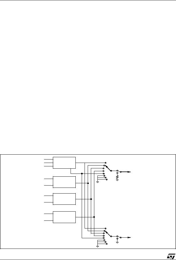
5.1Input stages
In the basic configuration, one stereo quasi-differential and three (two in case of DSO applications) single ended stereo inputs are available.
5.1.1 Quasi-differential stereo Input (QD)
The QD input is implemented as a buffered quasi-differential stereo stage with 100k input-impedance at each input. The attenuation is fixed to -3dB in order to adapt the incoming signal level.
5.1.2 Single-ended stereo input (SE1, SE2, SE3/AC2IN)
The input-impedance at each input is 100k and the attenuation is fixed to -3dB for incoming signals. The input for SE3 is also configurable as part of the interface for external filters in DSO applications (AC2IN)
Figure 4. Input Stage
QD_L
QD_G
QD_R
SE1_L
SE1_R
SE2_L
SE2_R
AC2IN_L/SE3L
AC2IN_R/SE3R
QD
SE1
SE2
SE3
QD |
Main |
|
Source |
SE4 |
In Gain |
SE1 |
|
SE2 |
|
SE3 |
|
|
Second |
|
Source |
Output Stage
8/30

TDA7419
5.2AutoZero
The AutoZero allows a reduction of the number of pins as well as external components by canceling any offset generated by or before the In-Gain-stage (Please notice that externally generated offsets, e.g. generated through the leakage current of the coupling capacitors, are not canceled).
The auto-zeroing is started every time the input source is changed and needs max. 0.3ms for the alignment. To avoid audible clicks the Audio processor is muted before the loudness stage during this time. The AutoZero feature is only present in the main signal-path.
5.2.1 AutoZero-Remain
In some cases, for example if the P is executing a refresh cycle of the IIC-Bus-programming, it is not useful to start a new AutoZero-action because no new source is selected and an undesired mute would appear at the outputs. For such applications, it can be switched in the AutoZero-Remain-Mode (Bit 6 of the subaddress-byte). If this bit is set to high, the AutoZero will not be invoked and the old adjustment-value remains.
5.3Loudness
There are four parameters programmable in the loudness stage:
5.3.1 Attenuation
Figure 5 shows the attenuation as a function of frequency at fP = 400Hz
Figure 5. Loudness Attenuation @ fP = 400Hz. |
|
|
|
5 |
|
|
|
0 |
|
|
|
-5 |
|
|
|
-10 |
|
|
|
-15 |
|
|
|
-20 |
|
|
|
10 |
100 |
1K |
10K |
9/30

TDA7419
5.3.2 Peakr Frequency
Figure 6 shows the three possible peak-frequencies 400Hz , 800Hz and 2.4kHz.
Figure 6. Loudness Center frequencies @ Attn. = 15dB
5 |
|
|
|
0 |
|
|
|
-5 |
|
|
|
-10 |
|
|
|
-15 |
|
|
|
-20 |
|
|
|
10 |
100 |
1K |
10K |
5.3.3 Low & High Frequency Boost
Figure 7 shows the different Loudness-shapes in low & high frequency boost.
Figure 7. Loudness Attenuation , fC = 2.4KHz |
|
|
|
5 |
|
|
|
0 |
|
|
|
-5 |
|
|
|
-10 |
|
|
|
-15 |
|
|
|
-20 |
|
|
|
10 |
100 |
1K |
10K |
10/30 |
|
|
|
Loading...